JP2004226593A - Photomask blank, its manufacturing method, and photomask - Google Patents
Photomask blank, its manufacturing method, and photomask Download PDFInfo
- Publication number
- JP2004226593A JP2004226593A JP2003013162A JP2003013162A JP2004226593A JP 2004226593 A JP2004226593 A JP 2004226593A JP 2003013162 A JP2003013162 A JP 2003013162A JP 2003013162 A JP2003013162 A JP 2003013162A JP 2004226593 A JP2004226593 A JP 2004226593A
- Authority
- JP
- Japan
- Prior art keywords
- film
- phase shift
- photomask blank
- photomask
- light
- Prior art date
- Legal status (The legal status is an assumption and is not a legal conclusion. Google has not performed a legal analysis and makes no representation as to the accuracy of the status listed.)
- Granted
Links
Images


Abstract
Description
【0001】
【発明の属する技術分野】
本発明は、半導体集積回路、CCD(電荷結合素子)、LCD(液晶表示素子)用カラーフィルター、及び磁気ヘッド等の微細加工に用いられるフォトマスクブランク及びフォトマスクに関する。
【0002】
【従来の技術】
IC及びLSI等の半導体集積回路の製造をはじめとして、広範囲な用途に用いられているフォトマスクは、基本的には透光性基板上にクロム等の遮光膜を所定のパターンで形成したものである。近年では半導体集積回路の高集積化などの市場要求に伴ってパターンの微細化が急速に進み、これに対して露光波長の短波長化を図ることにより対応してきた。
【0003】
しかしながら、露光波長の短波長化は解像度を改善する反面、焦点深度の減少を招き、プロセスの安定性が低下し、製品の歩留まりに悪影響を及ぼすという問題があった。
【0004】
このような問題に対して有効なパターン転写法の一つとして位相シフト法があり、微細パターンを転写するためのマスクとして位相シフトマスクが使用されている。位相シフトマスクは、透過する部位によって光の位相を変え、位相の異なる光の干渉を利用して微細なパターンを形成するものである。
【0005】
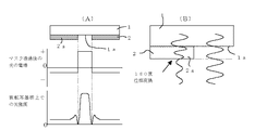
位相シフトマスクは、例えば、図6(A),(B)に示したように、基板1上の位相シフト膜2をパターン形成してなるもので、位相シフト膜が存在しない基板露出部(第1光透過部)1aとマスク上のパターン部分を形成している位相シフター部(第2光透過部)2aとにおいて、両者を透過してくる光の位相差を図6(B)に示したように180°とすることで、パターン境界部分の光の干渉により、干渉した部分で光強度はゼロとなり、転写像のコントラストを向上させることができるものである。また、位相シフト法を用いることにより、必要な解像度を得る際の焦点深度を増大させることが可能となり、クロム膜等からなる一般的な露光パターンをもつ通常のマスクを用いた場合に比べて、解像度の改善と露光プロセスのマージンを向上させることが可能なものである。
【0006】
上記位相シフトマスクは、位相シフター部の光透過特性によって、完全透過型位相シフトマスクと、ハーフトーン型位相シフトマスクとに、実用的には大別することができる。完全透過型位相シフトマスクは、位相シフター部の光透過率が基板と同等であり、露光波長に対し透明なマスクである。一方、ハーフトーン型位相シフトマスクは、位相シフター部の光透過率が基板露出部の数%〜数十%程度のものである。
【0007】
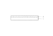
図1にハーフトーン型位相シフトマスクブランク、図2にハーフトーン型位相シフトマスクの基本的な構造をそれぞれ示す。図1に示したハーフトーン型位相シフトマスクブランクは、露光光に対して透明な基板1上にハーフトーン型位相シフト膜2を形成したものである。また、図2に示したハーフトーン型位相シフトマスクは、上記シフト膜2をパターニングして、マスク上のパターン部分を形成するハーフトーン型位相シフター部2aと、位相シフト膜が存在しない基板露出部1aを形成したものである。
【0008】
ここで、位相シフター部2aを透過した露光光は基板露出部1aを透過した露光光に対して位相がシフトされる(図6(A),(B)参照)。また、位相シフター部2aを透過した露光光が被転写基板上のレジストに対しては感光しない程度の光強度になるように、位相シフター部2aの透過率は設定されている。従って、位相シフター部2aは露光光を実質的に遮光する機能を有する。
【0009】
上記ハーフトーン型位相シフトマスクとしては、構造が簡単な単層型のハーフトーン型位相シフトマスクが提案されており、このような単層型のハーフトーン型位相シフトマスクとして、モリブデンシリサイド酸化物(MoSiO)、モリブデンシリサイド酸化窒化物(MoSiON)からなる位相シフト膜を有するものなどが提案されている(特許文献1:特開平7−140635号公報)。
【0010】
このような位相シフトマスクを製造する方法としては、位相シフトマスクブランクをリソグラフィ法によりパターン形成する方法が用いられる。このリソグラフィ法は、位相シフトマスクブランク上にレジストを塗布し、電子線又は紫外線により所望の部分のレジストを感光後に現像し、パターニングされたレジスト膜をマスクとして所望の部分の位相シフト膜をエッチングして基板を露出させ、その後、レジスト膜を剥離することにより位相シフトマスクが得るものである。
【0011】
しかしながら、上記位相シフトマスクブランクにおいては、通常、スパッタリングによって位相シフト膜等の膜が成膜されるが、この膜には応力が発生し、これにより基板が歪んでしまうため、得られるフォトマスクブランクには反りが発生する。このフォトマスクブランクをパターニングしてフォトマスクを製造すると、膜にパターニングした後に応力が解放されるため、基板の反りが成膜前の状態にある程度戻り、基板の平坦度が変化してしまう。この変化により、パターン露光時の設計と実際に出来上がったマスクとの間でパターンの寸法が変化してしまい、この寸法変化は、マスクパターンが微細なほど影響が大きくなってしまう。また、フォーカス位置のずれを生じさせることもある。
【0012】
更に、フォトマスクブランクからフォトマスクを製造する工程においては、表面の汚れ、異物等を洗浄するために硫酸等の酸やアンモニア水、アンモニアと過酸化水素水の混合液等のアルカリ溶液を用いるが、フォトマスクブランクやフォトマスクに用いられる膜は、酸、アルカリ等に対する耐薬品性が十分ではない場合が多く、特に、位相シフト膜にはアルカリ処理によって位相差が変化してしまうという問題もある。
【0013】
【特許文献1】
特開平7−140635号公報
【0014】
【発明が解決しようとする課題】
本発明は、上記問題点を解決するためになされたもので、反りが小さく、酸やアルカリに対する耐薬品性が高い高品位なフォトマスクブランク、その製造方法及びフォトマスクを提供することを目的とする。
【0015】
【課題を解決するための手段及び発明の実施の形態】
本発明者は、上記課題を解決するため鋭意検討を重ねた結果、透明基板上に少なくとも一層の膜を設けてなるフォトマスクブランクの膜による基板の反りが0.5μm以下であるフォトマスクブランク、特に、膜が位相シフト膜であり、29%のアンモニア水と31%の過酸化水素水と水とを体積比1:1:20で混合したアルカリ液に、30℃で10分間浸漬したときの位相変化量が2°以内であるフォトマスクブランクが、パターンの微細化に対応し得る高精度かつ高品位のフォトマスクを与えるフォトマスクブランクであり、このようなフォトマスクブランクが、透明基板上に少なくとも一層の膜を設けてなるフォトマスクブランクを製造する際、膜の成膜後に紫外線を含む光を照射することにより得られることを見出し、本発明をなすに至った。
【0016】
即ち、本発明は、下記のフォトマスクブランク及びフォトマスクを提供する。
請求項1:
透明基板上に少なくとも一層の膜を設けてなるフォトマスクブランクであって、膜による基板の反りが0.5μm以下であることを特徴とするフォトマスクブランク。
請求項2:
透明基板上に少なくとも一層の膜を設けてなるフォトマスクブランクであって、上記膜が位相シフト膜であり、かつ29%のアンモニア水と31%の過酸化水素水と水とを体積比1:1:20で混合したアルカリ液に、30℃で10分間浸漬したときの位相変化量が2°以内であることを特徴とするフォトマスクブランク。
請求項3:
位相変化量が1°以内であることを特徴とする請求項2記載のフォトマスクブランク。
請求項4:
膜がスパッタリングにより成膜されたものであることを特徴とする請求項1乃至3のいずれか1項記載のフォトマスクブランク。
請求項5:
位相シフト膜がケイ素と少なくとも1種のケイ素以外の金属とを含み、更に酸素、炭素又は窒素の少なくとも1種を含むことを特徴とする請求項2乃至4のいずれか1項記載のフォトマスクブランク。
請求項6:
透明基板上に少なくとも一層の膜を設けてなるフォトマスクブランクの製造方法であって、成膜後に紫外線を含む光を照射することを特徴とするフォトマスクブランクの製造方法。
請求項7:
照射する光の膜に対する吸収率が基板に対する吸収率より大きいことを特徴とする請求項6記載のフォトマスクブランクの製造方法。
請求項8:
請求項1乃至5のいずれか1項記載のフォトマスクブランクの膜上にフォトリソグラフィー法にてレジストパターンを形成した後、エッチング法にて膜のレジスト非被覆部分を除去し、次いでレジストを除去して得たことを特徴とするフォトマスク。
【0017】
本発明によれば、フォトマスクブランクの反りを低減することができると共に、フォトマスクブランクやフォトマスクの膜の酸やアルカリに対する耐薬品性を改善すること、特に、位相シフト膜のアルカリ処理による位相差の変化を抑えることができる。
【0018】
以下、本発明について更に詳しく説明する。
本発明のフォトマスクブランクは、透明基板上に少なくとも一層の膜を設けてなるフォトマスクブランクであり、膜による基板の反りが0.5μm以下、好ましくは0.3μm以下のものである。なお、反りとは、非吸着での表面高さの全測定点データから算出される最小二乗平面を基準面とした表面高さの最大値と最小値との差を意味するものである。
【0019】
また、本発明のフォトマスクブランクは、透明基板上に少なくとも一層の膜を設けてなるフォトマスクブランクであり、上記膜が位相シフト膜であり、かつアンモニアと過酸化水素とを含むアルカリ水溶液に浸漬したとき、特に29%のアンモニア水と31%の過酸化水素水と水とを体積比1:1:20で混合したアルカリ液に、30℃で10分間浸漬したときの位相変化量が2°以内、特に1°以内のものである。
【0020】
このようなフォトマスクブランクは、石英、CaF2等の露光光が透過する基板上に、遮光膜、位相シフト膜等の膜を成膜した後に、紫外線を含む光を照射することにより得ることができる。この場合、特に、照射する光の膜に対する吸収率が基板に対する吸収率より大きい光を用いることが好ましい。
【0021】
遮光膜、位相シフト膜等を成膜した後に紫外線を含む光を照射することで、膜質が改善される。膜質が改善される理由は、これに限定されるものではないが、紫外線の吸収による変化、急激な膜の温度変化、或いはそれらが組み合わさり、膜の原子の結合状態、欠陥の量、表面組成(例えば、酸化度や窒化度)等が変化したことによるものと考えられる。
【0022】
照射する光を発光するランプの種類としては、紫外線ランプや紫外線レーザーを挙げることができ、特に、紫外線ランプが好ましく用いられる。
【0023】
光を照射するときの雰囲気はアルゴン等の不活性ガス中、窒素中、酸素中、これらガスの2種以上の混合ガス中、真空中、大気中など特に制約はないが、膜の酸化、窒化等を望むときは、酸素、窒素を含む雰囲気中で、膜の酸化、窒化を嫌うときは不活性ガス中又は真空中で光を照射すればよい。
【0024】
本発明において、成膜した膜に光を照射する場合、1回で照射が完了するように照射しても、複数回に分けて照射してもよい。また、膜を多層構造にする場合には、膜を成膜する毎に照射することも、複数の膜を成膜してからまとめて照射することも可能である。特に、基板に位相シフト膜を成膜し、更に遮光膜や反射防止膜、例えばCr膜等の金属膜を形成した位相シフトマスクブランクを製造する場合は、位相シフト膜を形成した後に光を照射し、その後に金属膜を形成することが好ましい。
【0025】
一方、基板への位相シフト膜、遮光膜、反射防止膜等の成膜には、公知の方法を用いることが可能であるが、本発明においては、スパッタリング法により膜を成膜したものに対する反りの低減や耐薬品性向上の効果が大きいため好ましい。スパッタリングの方法としては、膜に酸素、窒素、炭素等の軽元素を含有させるときには、反応性スパッタリング法が好ましく、所定の組成のターゲットを用い、必要とする上記軽元素を含むスパッタリングガス雰囲気下でスパッタリングすることにより成膜することができる。
【0026】
この場合、膜を成膜する際のスパッタリングガスとしては、アルゴン等の不活性ガスに酸素、窒素、各種酸化窒素、各種酸化炭素等の酸素、窒素、炭素等を含むガスを成膜される膜が所望の組成となるように適宜添加することができる。
【0027】
また、スパッタリング方式としては、直流(DC)電源を用いたものでも、高周波(RF)電源を用いたものでもよく、またマグネトロンスパッタリング方式であっても、コンベンショナル方式であってもよい。なお、成膜装置は通過型でも枚葉型でも構わない。
【0028】
本発明において、紫外線を含む光を照射する膜は、フォトマスクブランクとして基板上に成膜する膜であれば特に限定されず、位相シフト膜、遮光膜、反射防止膜等を挙げることができるが、位相シフト膜が好ましく、特に露光光に対する吸収率が基板より大きい膜、とりわけハーフトーン型の位相シフト膜は、薬液処理によるわずかな膜の変化を嫌うため、光照射の効果が大きく好ましい。
【0029】
位相シフト膜としては、例えばケイ素と少なくとも1種以上のケイ素以外の金属とを含むもの、更にはこれらに酸素、窒素、炭素のいずれか、又は2種以上を含むものが好ましい。また、上記ケイ素以外の金属としてはW、Mo、Ti、Ta、Zr、Hf、Nb、V、Co、Cr又はNi等が挙げられるが、Moをベースにしたものが反りの低減や耐薬品性向上の効果が大きく、特にモリブデンシリサイド酸化物(MoSiO)、モリブデンシリサイド窒化物(MoSiN)、モリブデンシリサイド炭化物(MoSiC)、モリブデンシリサイド酸化窒化物(MoSiON)、モリブデンシリサイド酸化炭化物(MoSiOC)又はモリブデンシリサイド酸化窒化炭化物(MoSiONC)からなることが好ましい。このようなモリブデンシリサイド系の位相シフト膜は、ターゲットとしてMoSi等を用いた反応性スパッタリング法により成膜することができる。
【0030】
また、位相シフト膜の厚さは、位相シフトマスク使用時の露光波長や位相シフト層の透過率や位相シフト量等によっても異なるが、通常50〜200nm、特に50〜130nmであることが好ましい。
【0031】
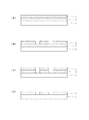
なお、図3,4に示すように、位相シフト膜2上に、遮光膜3を設けること、更には遮光膜3からの反射を低減させる反射防止膜4を上記遮光膜3上に形成することもできる。
【0032】
この場合、遮光膜又は反射防止膜としてはクロム酸化炭化物(CrOC)、クロム酸化窒化炭化物(CrONC)等のクロム系の膜又はこれらを積層したものを用いることができる。
【0033】
このようなCr系遮光膜又はCr系反射防止膜は、例えば、クロム単体又はクロムに酸素、窒素、炭素のいずれか又はこれらを組み合わせて添加したクロム化合物をターゲットとして用い、アルゴン、クリプトン等の不活性ガスに炭素源として一酸化炭素ガス、二酸化炭素ガスや、メタンなどの炭化水素ガスを添加したスパッタリングガスを用いた反応性スパッタリングにより成膜することができる。
【0034】
本発明のフォトマスクは、上記フォトマスクブランクの膜をパターン形成してなるものである。例えば、膜が位相シフト膜の場合は、図2に示したように、パターン化された位相シフター部間が第1光透過部1a(基板露出部)、パターン化された位相シフター部が第2光透過部2aとなる。
【0035】
位相シフトマスクを製造する場合、具体的には、図5に示すように、上記のようにして基板1上に位相シフト膜2を形成した位相シフトマスクブランクに、更にレジスト膜5を形成し、レジスト膜5をリソグラフィ法によりパターンニングし、更に、位相シフト膜2をエッチングした後、レジスト膜5を剥離する方法が採用し得る。この場合、レジスト膜の塗布、パターンニング(露光、現像)、エッチング、レジスト膜の除去は、公知の方法によって行うことができる。
【0036】
【実施例】
以下、実施例及び比較例を示し、本発明を具体的に説明するが、本発明は下記実施例に制限されるものではない。
【0037】
[実施例1]
6”の角形石英基板上にMoSiONからなる位相シフト膜を、ターゲットにMoSi、スパッタリングガスとしてN2とO2を用いて反応性DCスパッタ法にて、位相差が180°となるように膜厚を調整して成膜した。この位相シフト膜の膜厚は1,030Å、透過率は248nmの光で6.3%であった。次に、この位相シフト膜に、400nm以下の波長の光を含みピーク波長が400〜500nmの光を発光するランプをAr雰囲気中で膜全体に照射して位相シフトマスクブランクを得た。
【0038】
この位相シフトマスクブランクの膜による基板の反りを測定したところ、引張応力による0.42μmの反りであった。また、この位相シフトマスクブランクを29%のアンモニア水と31%の過酸化水素水と純水とを体積比で1:1:20で混合したアルカリ液に、30℃で10分間浸漬した後の位相差を測定したところ、浸漬前後の位相差の変化量は1.1°以下であった。なお、反りはニデック社製FT−900を用いて測定した(以下同じ)。
【0039】
[比較例1]
実施例1において、位相シフト膜の成膜後にランプを照射せずに位相シフトマスクブランクを得、その反りを測定したところ、圧縮応力による0.9μmの反りであった。また、この位相シフトマスクブランクを実施例1と同様の方法でアルカリ液への浸漬してその位相差を測定したところ、浸漬前後の位相差の変化量は4.9°であった。
【0040】
【発明の効果】
以上説明したように、本発明によれば、反りが小さく、酸やアルカリに対する耐薬品性が高い高品質なフォトマスクブランク及びフォトマスクが得られる。
【図面の簡単な説明】
【図1】本発明の一実施例に係る位相シフトマスクブランクの断面図である。
【図2】本発明の一実施例に係る位相シフトマスクの断面図である。
【図3】本発明の一実施例に係る遮光膜を設けた位相シフトマスクブランクの断面図である。
【図4】本発明の一実施例に係る遮光膜及び反射防止膜を設けた位相シフトマスクブランクの断面図である。
【図5】位相シフトマスクの製造法を示した説明図であり、(A)はレジスト膜を形成した状態、(B)はレジスト膜をパターンニングした状態、(C)は位相シフト膜のエッチングを行った状態、(D)はレジスト膜を除去した状態の概略断面図である。
【図6】(A),(B)はハーフトーン型位相シフトマスクの原理を説明する図であり、(B)は(A)の部分拡大図である。
【符号の説明】
1 基板
1a 基板露出部(第1光透過部)
2 位相シフト膜
2a 位相シフター部(第2光透過部)
3 遮光膜
4 反射防止膜
5 レジスト膜[0001]
TECHNICAL FIELD OF THE INVENTION
The present invention relates to a photomask blank and a photomask used for fine processing of a semiconductor integrated circuit, a color filter for a CCD (charge coupled device), an LCD (liquid crystal display device), a magnetic head, and the like.
[0002]
[Prior art]
Photomasks used for a wide range of applications, including the manufacture of semiconductor integrated circuits such as ICs and LSIs, are basically formed by forming a light-shielding film such as chromium on a light-transmitting substrate in a predetermined pattern. is there. In recent years, pattern miniaturization has rapidly progressed in response to market requirements such as higher integration of semiconductor integrated circuits, and this has been dealt with by shortening the exposure wavelength.
[0003]
However, while shortening the exposure wavelength improves resolution, it also causes a decrease in the depth of focus, resulting in a decrease in process stability and a negative effect on product yield.
[0004]
One effective pattern transfer method for such a problem is a phase shift method, and a phase shift mask is used as a mask for transferring a fine pattern. The phase shift mask changes the phase of light depending on the portion to be transmitted, and forms a fine pattern using interference of light having different phases.
[0005]
The phase shift mask is formed by patterning a
[0006]
The above-mentioned phase shift masks can be practically classified into a complete transmission type phase shift mask and a halftone type phase shift mask according to the light transmission characteristics of the phase shifter. The complete transmission type phase shift mask is a mask which has the same light transmittance of the phase shifter portion as the substrate and is transparent to the exposure wavelength. On the other hand, in a halftone phase shift mask, the light transmittance of the phase shifter is about several percent to several tens of percent of the exposed part of the substrate.
[0007]
FIG. 1 shows a basic structure of a halftone type phase shift mask blank, and FIG. 2 shows a basic structure of a halftone type phase shift mask. The halftone type phase shift mask blank shown in FIG. 1 has a halftone type
[0008]
Here, the phase of the exposure light transmitted through the phase shifter 2a is shifted with respect to the exposure light transmitted through the substrate exposed portion 1a (see FIGS. 6A and 6B). The transmittance of the phase shifter 2a is set so that the exposure light transmitted through the phase shifter 2a has a light intensity that does not expose the resist on the transfer target substrate. Therefore, the phase shifter 2a has a function of substantially blocking the exposure light.
[0009]
As the halftone phase shift mask, a single-layer halftone phase shift mask having a simple structure has been proposed. As such a single-layer halftone phase shift mask, molybdenum silicide oxide ( A device having a phase shift film made of MoSiO) or molybdenum silicide oxynitride (MoSiON) has been proposed (Patent Document 1: JP-A-7-140635).
[0010]
As a method of manufacturing such a phase shift mask, a method of forming a pattern on a phase shift mask blank by a lithography method is used. In this lithography method, a resist is applied on a phase shift mask blank, a desired portion of the resist is exposed to light by an electron beam or ultraviolet light, developed, and the desired portion of the phase shift film is etched using the patterned resist film as a mask. Then, the substrate is exposed, and then the resist film is peeled off to obtain a phase shift mask.
[0011]
However, in the above-mentioned phase shift mask blank, a film such as a phase shift film is usually formed by sputtering. However, stress is generated in this film and the substrate is distorted by this. Is warped. When a photomask is manufactured by patterning this photomask blank, the stress is released after patterning into a film, so that the warpage of the substrate returns to a state before film formation to some extent, and the flatness of the substrate changes. Due to this change, the dimension of the pattern changes between the design at the time of pattern exposure and the actually completed mask, and the dimensional change has a greater effect as the mask pattern becomes finer. In addition, the focus position may be shifted.
[0012]
Further, in the process of manufacturing a photomask from a photomask blank, an acid such as sulfuric acid or an aqueous solution of ammonia, or an alkaline solution such as a mixed solution of ammonia and hydrogen peroxide is used to clean surface dirt and foreign matter. In addition, films used for photomask blanks and photomasks often have insufficient chemical resistance to acids, alkalis, and the like, and in particular, phase shift films have a problem that the phase difference is changed by alkali treatment. .
[0013]
[Patent Document 1]
JP-A-7-140635
[Problems to be solved by the invention]
The present invention has been made in order to solve the above problems, and has an object to provide a high-quality photomask blank having a small warpage and high chemical resistance to acids and alkalis, a method for manufacturing the same, and a photomask. I do.
[0015]
Means for Solving the Problems and Embodiments of the Invention
The present inventor has conducted intensive studies in order to solve the above problems, and as a result, a photomask blank in which the warpage of the substrate due to the film of the photomask blank in which at least one layer is provided on a transparent substrate is 0.5 μm or less, In particular, when the film is a phase shift film, the film is immersed in an alkaline solution in which 29% ammonia water, 31% hydrogen peroxide solution and water are mixed at a volume ratio of 1: 1: 20 at 30 ° C. for 10 minutes. A photomask blank having a phase change of 2 ° or less is a photomask blank that provides a high-precision and high-quality photomask that can respond to pattern miniaturization, and such a photomask blank is formed on a transparent substrate. When manufacturing a photomask blank provided with at least one layer of film, the present invention has been found to be obtained by irradiating light containing ultraviolet rays after film formation, and the present invention has been made. Reached.
[0016]
That is, the present invention provides the following photomask blank and photomask.
Claim 1:
What is claimed is: 1. A photomask blank comprising a transparent substrate provided with at least one layer of a film, wherein a warpage of the substrate due to the film is 0.5 μm or less.
Claim 2:
What is claimed is: 1. A photomask blank comprising at least one film provided on a transparent substrate, wherein said film is a phase shift film, and 29% ammonia water, 31% hydrogen peroxide solution and water are mixed at a volume ratio of 1: A photomask blank, wherein a phase change amount when immersed in an alkaline solution mixed at 1:20 at 30 ° C. for 10 minutes is within 2 °.
Claim 3:
3. The photomask blank according to
Claim 4:
The photomask blank according to any one of
Claim 5:
The photomask blank according to any one of
Claim 6:
What is claimed is: 1. A method for manufacturing a photomask blank comprising a transparent substrate and at least one layer provided thereon, wherein the method includes irradiating light including ultraviolet rays after film formation.
Claim 7:
7. The method for manufacturing a photomask blank according to claim 6, wherein the absorptance of the irradiated light to the film is larger than the absorptance to the substrate.
Claim 8:
A resist pattern is formed on the film of the photomask blank according to any one of
[0017]
According to the present invention, the warpage of the photomask blank can be reduced, and the chemical resistance of the photomask blank and the film of the photomask to acid and alkali can be improved. The change in the phase difference can be suppressed.
[0018]
Hereinafter, the present invention will be described in more detail.
The photomask blank of the present invention is a photomask blank in which at least one film is provided on a transparent substrate, and has a substrate warpage of 0.5 μm or less, preferably 0.3 μm or less. The warp means a difference between the maximum value and the minimum value of the surface height using the least square plane calculated as the reference surface, which is calculated from all the measurement data of the surface height without suction.
[0019]
Further, the photomask blank of the present invention is a photomask blank in which at least one layer is provided on a transparent substrate, wherein the layer is a phase shift film, and is immersed in an alkaline aqueous solution containing ammonia and hydrogen peroxide. In particular, the phase change when immersed at 30 ° C. for 10 minutes in an alkaline solution obtained by mixing 29% ammonia water, 31% hydrogen peroxide solution and water at a volume ratio of 1: 1: 20 is 2 °. Less than 1 °.
[0020]
Such a photomask blank can be obtained by forming a film such as a light-shielding film and a phase shift film on a substrate through which exposure light such as quartz or CaF 2 is transmitted, and then irradiating the film with ultraviolet light. it can. In this case, it is particularly preferable to use light whose absorptance of the irradiated light to the film is higher than that of the substrate.
[0021]
By irradiating light including ultraviolet rays after forming the light shielding film, the phase shift film, and the like, the film quality is improved. The reasons for the improvement of the film quality are not limited thereto, but include changes due to absorption of ultraviolet rays, rapid changes in the temperature of the film, or a combination thereof, the bonding state of atoms in the film, the amount of defects, and the surface composition. (Eg, the degree of oxidation or the degree of nitridation) is considered to be due to a change.
[0022]
Examples of the type of lamp that emits light for irradiation include an ultraviolet lamp and an ultraviolet laser, and an ultraviolet lamp is particularly preferably used.
[0023]
The atmosphere for light irradiation is not particularly limited, such as in an inert gas such as argon, in nitrogen, in oxygen, in a mixed gas of two or more of these gases, in a vacuum, or in the atmosphere. When it is desired to do so, light irradiation may be performed in an atmosphere containing oxygen or nitrogen, or in an inert gas or vacuum if the oxidation or nitridation of the film is not desired.
[0024]
In the present invention, when the film is irradiated with light, the light may be irradiated so as to complete the irradiation in one time or may be irradiated in a plurality of times. When the film has a multilayer structure, irradiation can be performed each time a film is formed, or irradiation can be performed collectively after forming a plurality of films. In particular, when manufacturing a phase shift mask blank in which a phase shift film is formed on a substrate and further a light shielding film or an antireflection film, for example, a metal film such as a Cr film is formed, light is irradiated after forming the phase shift film. After that, it is preferable to form a metal film.
[0025]
On the other hand, a known method can be used for forming a phase shift film, a light-shielding film, an anti-reflection film, and the like on a substrate, but in the present invention, warpage of a film formed by a sputtering method is obtained. It is preferable because the effect of reducing the chemical resistance and improving the chemical resistance is great. As a method of sputtering, when a light element such as oxygen, nitrogen, or carbon is contained in the film, a reactive sputtering method is preferable, and a target having a predetermined composition is used, and under a sputtering gas atmosphere containing the required light element. A film can be formed by sputtering.
[0026]
In this case, as a sputtering gas for forming the film, a film containing a gas containing oxygen, nitrogen, various kinds of nitrogen oxide, various kinds of carbon oxides, etc., oxygen, nitrogen, carbon, or the like in an inert gas such as argon. Can be appropriately added so as to have a desired composition.
[0027]
Further, as a sputtering method, a method using a direct current (DC) power supply or a method using a high frequency (RF) power supply may be used, and a magnetron sputtering method or a conventional method may be used. Note that the film forming apparatus may be a passing type or a single wafer type.
[0028]
In the present invention, the film irradiated with light including ultraviolet light is not particularly limited as long as it is a film formed on a substrate as a photomask blank, and examples thereof include a phase shift film, a light shielding film, and an antireflection film. In particular, a film having a higher absorptance to the exposure light than the substrate, particularly a halftone type phase shift film, dislikes a slight change in the film due to the treatment with a chemical solution, and therefore has a large effect of light irradiation, and is therefore preferable.
[0029]
As the phase shift film, for example, those containing silicon and at least one or more metals other than silicon, and those containing any one or more of oxygen, nitrogen and carbon are preferable. Examples of the metal other than silicon include W, Mo, Ti, Ta, Zr, Hf, Nb, V, Co, Cr, and Ni, and those based on Mo reduce warpage and improve chemical resistance. The effect of improvement is great, especially molybdenum silicide oxide (MoSiO), molybdenum silicide nitride (MoSiN), molybdenum silicide carbide (MoSiC), molybdenum silicide oxynitride (MoSiON), molybdenum silicide oxycarbide (MoSiOC) or molybdenum silicide oxide It is preferable to be made of nitrided carbide (MoSiONC). Such a molybdenum silicide-based phase shift film can be formed by a reactive sputtering method using MoSi or the like as a target.
[0030]
The thickness of the phase shift film varies depending on the exposure wavelength when the phase shift mask is used, the transmittance of the phase shift layer, the amount of phase shift, and the like, but is usually preferably 50 to 200 nm, particularly preferably 50 to 130 nm.
[0031]
As shown in FIGS. 3 and 4, a light shielding film 3 is provided on the
[0032]
In this case, a chromium-based film such as chromium oxycarbide (CrOC) or chromium oxynitride carbide (CrONC) or a laminate of these can be used as the light-shielding film or the antireflection film.
[0033]
Such a Cr-based light-shielding film or Cr-based antireflection film uses, as a target, for example, chromium alone or a chromium compound obtained by adding any one of oxygen, nitrogen, and carbon to chromium, and uses a chromium compound such as argon or krypton. A film can be formed by reactive sputtering using a sputtering gas in which a carbon gas such as carbon monoxide gas, carbon dioxide gas, or methane is added as a carbon source to an active gas.
[0034]
The photomask of the present invention is obtained by patterning the film of the photomask blank. For example, when the film is a phase shift film, as shown in FIG. 2, the space between the patterned phase shifter portions is the first light transmission portion 1a (substrate exposed portion), and the patterned phase shifter portion is the second light shift portion. It becomes the light transmitting portion 2a.
[0035]
When manufacturing the phase shift mask, specifically, as shown in FIG. 5, a resist
[0036]
【Example】
Hereinafter, the present invention will be described specifically with reference to Examples and Comparative Examples, but the present invention is not limited to the following Examples.
[0037]
[Example 1]
A phase shift film made of MoSiON is formed on a 6 ″ square quartz substrate using MoSi as a target and N 2 and O 2 as a sputtering gas by a reactive DC sputtering method so that the phase difference becomes 180 °. The phase shift film had a film thickness of 1,030 ° and a transmittance of 6.3% for light of 248 nm. A phase shift mask blank was obtained by irradiating the entire film with a lamp that emits light having a peak wavelength of 400 to 500 nm in an Ar atmosphere.
[0038]
When the warpage of the substrate due to the film of the phase shift mask blank was measured, the warpage was 0.42 μm due to the tensile stress. Further, this phase shift mask blank was immersed in an alkaline solution in which 29% ammonia water, 31% hydrogen peroxide solution and pure water were mixed at a volume ratio of 1: 1: 20 at 30 ° C. for 10 minutes. When the phase difference was measured, the amount of change in the phase difference before and after immersion was 1.1 ° or less. The warpage was measured using Nidek FT-900 (the same applies hereinafter).
[0039]
[Comparative Example 1]
In Example 1, after forming the phase shift film, a phase shift mask blank was obtained without irradiating a lamp, and the warpage was measured. As a result, the warp was 0.9 μm due to compressive stress. The phase shift mask blank was immersed in an alkaline solution in the same manner as in Example 1, and the phase difference was measured. The change in the phase difference before and after immersion was 4.9 °.
[0040]
【The invention's effect】
As described above, according to the present invention, a high-quality photomask blank and a photomask having small warpage and high chemical resistance to acids and alkalis can be obtained.
[Brief description of the drawings]
FIG. 1 is a sectional view of a phase shift mask blank according to one embodiment of the present invention.
FIG. 2 is a sectional view of a phase shift mask according to one embodiment of the present invention.
FIG. 3 is a cross-sectional view of a phase shift mask blank provided with a light shielding film according to one embodiment of the present invention.
FIG. 4 is a cross-sectional view of a phase shift mask blank provided with a light shielding film and an anti-reflection film according to one embodiment of the present invention.
5A and 5B are explanatory diagrams showing a method of manufacturing a phase shift mask, wherein FIG. 5A shows a state in which a resist film is formed, FIG. 5B shows a state in which the resist film is patterned, and FIG. (D) is a schematic cross-sectional view of a state where the resist film is removed.
6A and 6B are diagrams for explaining the principle of a halftone type phase shift mask, and FIG. 6B is a partially enlarged view of FIG.
[Explanation of symbols]
1 Substrate 1a Substrate exposed part (first light transmitting part)
2 Phase shift film 2a Phase shifter section (second light transmitting section)
3
Claims (8)
Priority Applications (1)
| Application Number | Priority Date | Filing Date | Title |
|---|---|---|---|
| JP2003013162A JP4026000B2 (en) | 2003-01-22 | 2003-01-22 | Method for manufacturing photomask blank, method for reducing warpage, method for improving chemical resistance of film, and photomask |
Applications Claiming Priority (1)
| Application Number | Priority Date | Filing Date | Title |
|---|---|---|---|
| JP2003013162A JP4026000B2 (en) | 2003-01-22 | 2003-01-22 | Method for manufacturing photomask blank, method for reducing warpage, method for improving chemical resistance of film, and photomask |
Publications (2)
| Publication Number | Publication Date |
|---|---|
| JP2004226593A true JP2004226593A (en) | 2004-08-12 |
| JP4026000B2 JP4026000B2 (en) | 2007-12-26 |
Family
ID=32901568
Family Applications (1)
| Application Number | Title | Priority Date | Filing Date |
|---|---|---|---|
| JP2003013162A Expired - Lifetime JP4026000B2 (en) | 2003-01-22 | 2003-01-22 | Method for manufacturing photomask blank, method for reducing warpage, method for improving chemical resistance of film, and photomask |
Country Status (1)
| Country | Link |
|---|---|
| JP (1) | JP4026000B2 (en) |
Cited By (5)
| Publication number | Priority date | Publication date | Assignee | Title |
|---|---|---|---|---|
| JP2005331554A (en) * | 2004-05-18 | 2005-12-02 | Shin Etsu Chem Co Ltd | Photomask blank and method for manufacturing the photomask |
| JP2010066783A (en) * | 2009-12-25 | 2010-03-25 | Shin-Etsu Chemical Co Ltd | Photomask blank and method for manufacturing photomask |
| JP2011232605A (en) * | 2010-04-28 | 2011-11-17 | Hoya Corp | Multi-gradation photomask, method for manufacturing the same, pattern transfer method and method for using multi-gradation photomask |
| US8221941B2 (en) | 2008-12-29 | 2012-07-17 | Hoya Corporation | Photomask blank manufacturing method and photomask manufacturing method |
| JP2016033652A (en) * | 2014-07-30 | 2016-03-10 | 信越化学工業株式会社 | Method for designing photomask blank, and photomask blank |
-
2003
- 2003-01-22 JP JP2003013162A patent/JP4026000B2/en not_active Expired - Lifetime
Cited By (9)
| Publication number | Priority date | Publication date | Assignee | Title |
|---|---|---|---|---|
| JP2005331554A (en) * | 2004-05-18 | 2005-12-02 | Shin Etsu Chem Co Ltd | Photomask blank and method for manufacturing the photomask |
| JP4650608B2 (en) * | 2004-05-18 | 2011-03-16 | 信越化学工業株式会社 | Photomask blank and photomask manufacturing method |
| US8221941B2 (en) | 2008-12-29 | 2012-07-17 | Hoya Corporation | Photomask blank manufacturing method and photomask manufacturing method |
| JP2010066783A (en) * | 2009-12-25 | 2010-03-25 | Shin-Etsu Chemical Co Ltd | Photomask blank and method for manufacturing photomask |
| JP4687929B2 (en) * | 2009-12-25 | 2011-05-25 | 信越化学工業株式会社 | Photomask blank and photomask manufacturing method |
| JP2011232605A (en) * | 2010-04-28 | 2011-11-17 | Hoya Corp | Multi-gradation photomask, method for manufacturing the same, pattern transfer method and method for using multi-gradation photomask |
| JP2016033652A (en) * | 2014-07-30 | 2016-03-10 | 信越化学工業株式会社 | Method for designing photomask blank, and photomask blank |
| KR20190047671A (en) * | 2014-07-30 | 2019-05-08 | 신에쓰 가가꾸 고교 가부시끼가이샤 | Method of designing photomask blank, and photomask blank |
| KR102116205B1 (en) * | 2014-07-30 | 2020-05-27 | 신에쓰 가가꾸 고교 가부시끼가이샤 | Method of designing photomask blank, and photomask blank |
Also Published As
| Publication number | Publication date |
|---|---|
| JP4026000B2 (en) | 2007-12-26 |
Similar Documents
| Publication | Publication Date | Title |
|---|---|---|
| JP5554239B2 (en) | Photomask blank, photomask and manufacturing method thereof | |
| JP6264238B2 (en) | Halftone phase shift photomask blank, halftone phase shift photomask, and pattern exposure method | |
| JP5602930B2 (en) | Mask blank and transfer mask | |
| KR101586344B1 (en) | Photomask blank, photomask and fabrication method thereof | |
| TWI481949B (en) | Photomask blank, photomask, and methods of manufacturing these | |
| KR100843417B1 (en) | Methods of Manufacturing Photomask Blank and Photomask | |
| JP2007292824A (en) | Photomask blank | |
| WO2009123167A1 (en) | Photomask blank and method for manufacturing the same | |
| WO2009123166A1 (en) | Photomask blank and method for manufacturing the same | |
| TWI772645B (en) | Blank photomask, method for manufacturing photomask, and photomask | |
| JP2003050453A (en) | Phase shifting mask blank, phase shifting mask and method for producing those | |
| JP4739461B2 (en) | Method for manufacturing transfer mask and method for manufacturing semiconductor device | |
| WO2020241116A1 (en) | Photomask blank, method for producing photomask, and photomask | |
| JP2002258455A (en) | Phase shift mask blank and phase shift mask | |
| TW520462B (en) | Phase shift mask blank, phase shift mask, and methods of manufacturing the same | |
| JP4026000B2 (en) | Method for manufacturing photomask blank, method for reducing warpage, method for improving chemical resistance of film, and photomask | |
| JP4332697B2 (en) | Sputter target | |
| JP2018063441A (en) | Half tone phase shift type photomask blank, half tone phase shift type photomask and pattern exposure method | |
| JP5701946B2 (en) | Method for manufacturing phase shift mask | |
| JP6627926B2 (en) | Method for manufacturing phase shift mask blanks | |
| JP2010066783A (en) | Photomask blank and method for manufacturing photomask | |
| JP2002341515A (en) | Phase shifting mask blank, and method for producing phase shifting mask | |
| JP2022011477A (en) | Manufacturing method of photomask and photomask blank | |
| JP2003215778A (en) | Sputtering target, phase shift mask blank using this sputtering target, and method of manufacturing phase shift mask | |
| JP2002287323A (en) | Phase shifting mask blank, phase shifting mask and method for manufacturing the same |
Legal Events
| Date | Code | Title | Description |
|---|---|---|---|
| A621 | Written request for application examination |
Free format text: JAPANESE INTERMEDIATE CODE: A621 Effective date: 20041112 |
|
| A977 | Report on retrieval |
Free format text: JAPANESE INTERMEDIATE CODE: A971007 Effective date: 20070418 |
|
| A131 | Notification of reasons for refusal |
Free format text: JAPANESE INTERMEDIATE CODE: A131 Effective date: 20070425 |
|
| A521 | Request for written amendment filed |
Free format text: JAPANESE INTERMEDIATE CODE: A523 Effective date: 20070614 |
|
| TRDD | Decision of grant or rejection written | ||
| A01 | Written decision to grant a patent or to grant a registration (utility model) |
Free format text: JAPANESE INTERMEDIATE CODE: A01 Effective date: 20070912 |
|
| A61 | First payment of annual fees (during grant procedure) |
Free format text: JAPANESE INTERMEDIATE CODE: A61 Effective date: 20070925 |
|
| FPAY | Renewal fee payment (event date is renewal date of database) |
Free format text: PAYMENT UNTIL: 20101019 Year of fee payment: 3 |
|
| R150 | Certificate of patent or registration of utility model |
Ref document number: 4026000 Country of ref document: JP Free format text: JAPANESE INTERMEDIATE CODE: R150 Free format text: JAPANESE INTERMEDIATE CODE: R150 |
|
| FPAY | Renewal fee payment (event date is renewal date of database) |
Free format text: PAYMENT UNTIL: 20101019 Year of fee payment: 3 |
|
| FPAY | Renewal fee payment (event date is renewal date of database) |
Free format text: PAYMENT UNTIL: 20131019 Year of fee payment: 6 |
|
| EXPY | Cancellation because of completion of term |