JP2004222294A - Laser initialization in optical transceiver under control of firmware - Google Patents
Laser initialization in optical transceiver under control of firmware Download PDFInfo
- Publication number
- JP2004222294A JP2004222294A JP2004006909A JP2004006909A JP2004222294A JP 2004222294 A JP2004222294 A JP 2004222294A JP 2004006909 A JP2004006909 A JP 2004006909A JP 2004006909 A JP2004006909 A JP 2004006909A JP 2004222294 A JP2004222294 A JP 2004222294A
- Authority
- JP
- Japan
- Prior art keywords
- laser
- value
- bias current
- microcontroller
- monitor
- Prior art date
- Legal status (The legal status is an assumption and is not a legal conclusion. Google has not performed a legal analysis and makes no representation as to the accuracy of the status listed.)
- Withdrawn
Links
Images


Classifications
-
- H—ELECTRICITY
- H04—ELECTRIC COMMUNICATION TECHNIQUE
- H04B—TRANSMISSION
- H04B10/00—Transmission systems employing electromagnetic waves other than radio-waves, e.g. infrared, visible or ultraviolet light, or employing corpuscular radiation, e.g. quantum communication
- H04B10/50—Transmitters
- H04B10/564—Power control
-
- H—ELECTRICITY
- H04—ELECTRIC COMMUNICATION TECHNIQUE
- H04B—TRANSMISSION
- H04B10/00—Transmission systems employing electromagnetic waves other than radio-waves, e.g. infrared, visible or ultraviolet light, or employing corpuscular radiation, e.g. quantum communication
- H04B10/40—Transceivers
Abstract
Description
本発明は、一般に、光トランシーバ・モジュールに関するものであり、とりわけ、レーザ初期化性能(レーザ発光開始時の立ち上げ性能)を向上させるコントローラと連係動作する、レーザを備えた受信機及び送信機を用いる、光トランシーバ・モジュールに関するものである。 The present invention relates generally to an optical transceiver module, and more particularly to a laser-equipped receiver and transmitter that cooperates with a controller that improves laser initialization performance (start-up performance at the start of laser emission). The present invention relates to an optical transceiver module used.
データ通信における光ファイバ・テクノロジの利用は、急速なペースで拡大し続けている。コンピュータ、電話、及び、計測システムの接続には、光ファイバ伝送リンクが広く用いられている。光ファイバ・システムには、銅の導体を用いたシステムに対して途方もなく大きい利点がある。光ファイバ・システムは、銅による導体システムよりも小さく、軽いだけでなく、完全な電気絶縁性、極めて高速な広帯域機能、ノイズと広スペクトルの干渉の両方に対する完全なイミュニティ(耐性)をもたらす。最も重要なのは、光ファイバ通信リンクが、銅による導体システムよりはるかに低コストという点である。 The use of fiber optic technology in data communications continues to grow at a rapid pace. Optical fiber transmission links are widely used to connect computers, telephones, and measurement systems. Fiber optic systems have tremendous advantages over systems using copper conductors. Fiber optic systems are not only smaller and lighter than copper-based conductor systems, but also provide complete electrical insulation, extremely fast broadband capability, and full immunity to both noise and broad spectrum interference. Most importantly, fiber optic communication links are far less costly than copper based conductor systems.
基本的な光ファイバ通信リンクは、3つのコンポーネント、すなわち、送信機、受信機、及び、光ファイバ・ケーブルを備えている。送信機には、電流を光信号に変換する発光素子が含まれている。発光素子は、一般に、発光ダイオード、レーザ・ダイオード、または、面発光レーザ(VCSEL)である。受信機には、光信号を変換して、電流に戻す光検出素子が含まれている。光ファイバ・ケーブルは、送信機と受信機を接続し、それらの間で光信号を伝送する。 A basic fiber optic communication link has three components: a transmitter, a receiver, and a fiber optic cable. The transmitter includes a light emitting element that converts current into an optical signal. The light emitting device is typically a light emitting diode, a laser diode, or a surface emitting laser (VCSEL). The receiver includes a photodetector that converts the optical signal back into a current. Fiber optic cables connect transmitters and receivers and carry optical signals between them.
しかし、より一般的には、光ファイバ・リンクには、1対の光ファイバ・ケーブルによって結合された1対の光トランシーバが含まれている。光トランシーバは、送信機と受信機を組み合わせて、光データの送信と受信の両方に必要な、全ての所要の電気/光変換を可能にする一つのユニットをなすものである。第1のトランシーバの送信機は、一方の光ファイバ・ケーブルを介して、光信号の形をなすデータを第2のトランシーバの受信機に送り、第2の送信機は、引き続き、光信号を電気信号に変換する。同様に、第2のトランシーバの送信機は、もう一方の光ファイバ・ケーブルを介して、光信号を第1のトランシーバの受信機に送る。 However, more generally, a fiber optic link includes a pair of optical transceivers coupled by a pair of fiber optic cables. An optical transceiver combines a transmitter and a receiver into one unit that enables all necessary electrical / optical conversions necessary for both transmitting and receiving optical data. The transmitter of the first transceiver sends the data in the form of an optical signal to the receiver of the second transceiver via one fiber optic cable, and the second transmitter continues to transmit the optical signal to the receiver. Convert to a signal. Similarly, the transmitter of the second transceiver sends an optical signal to the receiver of the first transceiver via the other fiber optic cable.
発光素子としてレーザを利用する光トランシーバ・モジュールの場合、良質の製品が得られるようにするために、迅速かつ正確に実施しなければならない重要なタスクの1つが、レーザの初期化すなわち起動である。レーザが起動される毎に、確実に動作するため、その光出力パワー・レベルを所望のレンジすなわちウィンドウ内に上昇させ、安定化させなければならない。レーザの光出力パワー・レベルは、レーザに供給されるバイアス電流を調整することによって制御される。レーザの初期化は、一般に、光トランシーバ・モジュールがオンになる毎に、または、あるタイプのトランシーバ障害または発光禁止(ディゼイブル)が否定(解除)された後、実施される。トランシーバをできるだけ速く動作状態にするには、レーザの迅速な起動が望ましい。 In the case of optical transceiver modules that utilize lasers as light emitting elements, one of the key tasks that must be performed quickly and accurately in order to obtain a good product is the initialization or startup of the laser. . Each time the laser is activated, its light output power level must be raised and stabilized within the desired range or window to ensure operation. The light output power level of the laser is controlled by adjusting the bias current supplied to the laser. Laser initialization is typically performed each time the optical transceiver module is turned on, or after some type of transceiver fault or disable has been negated. In order to get the transceiver up and running as quickly as possible, it is desirable to have a fast activation of the laser.
従来、光トランシーバ・モジュールは、「ハード・コード」された(ハードウェアで組まれた)集積回路(IC)として構成されてきた。換言すれば、複数のトランジスタを含む個々の回路が、ICをなすように設計されており、各回路は、トランシーバの制御及び操作に関連した単一タスクを実施するためだけに用いられる。現在一般に行われているのは、レーザの初期化専用の回路に、レーザ・パワーに関する生成目標を記憶することである。起動時に、実際の光出力パワーが弱すぎる場合、回路は、バイアス電流をインクリメントする。同様に、光出力パワーが強すぎる場合、回路は、バイアス電流をデクリメントする。 Traditionally, optical transceiver modules have been configured as "hard coded" (hardware assembled) integrated circuits (ICs). In other words, individual circuits, including multiple transistors, are designed to be ICs, and each circuit is used only to perform a single task related to the control and operation of the transceiver. Currently, it is common practice to store generation targets for laser power in a circuit dedicated to laser initialization. At start-up, if the actual light output power is too weak, the circuit will increment the bias current. Similarly, if the optical output power is too strong, the circuit will decrement the bias current.
上述したアプローチの主たる欠点は、レーザ出力パワーを所望のウィンドウ内にするのに、数回にわたる繰り返しを必要とする場合があり、この結果、光トランシーバが光データを送信できるようになるのが遅れるという点である。初期化時に、レーザの光出力パワーをより迅速かつより正確に所望の動作ウィンドウ内の値にすることが可能な光トランシーバ・モジュールが必要とされている。 A major drawback of the above approach is that it may require several iterations to bring the laser output power into the desired window, which delays the ability of the optical transceiver to transmit optical data That is the point. There is a need for an optical transceiver module that, upon initialization, can more quickly and more accurately bring the laser's optical output power to a value within a desired operating window.
本発明の態様の1つによれば、レーザとコントローラを含む光トランシーバ・モジュールが得られる。レーザは、バイアス電流に基づくパワー・レベルを有する光出力信号を送り出すように構成されている。コントローラは、レーザに初期バイアス電流によるバイアスをかけ、パワー・レベルを表わすモニタ信号を受信し、パワー・レベルと目標パワー・レベル・レンジとを比較し、パワー・レベルが目標パワー・レベル・レンジ内になければ、レーザに調整されたバイアス電流によるバイアスをかける(すなわち、バイアスを調整する)ように構成されている。 According to one aspect of the present invention, there is provided an optical transceiver module including a laser and a controller. The laser is configured to emit an optical output signal having a power level based on the bias current. The controller biases the laser with the initial bias current, receives a monitor signal representing the power level, compares the power level with the target power level range, and determines that the power level is within the target power level range. Otherwise, the laser is biased by the adjusted bias current (ie, the bias is adjusted).
望ましい実施態様に関する下記の詳細な説明では、その一部をなし、例証として、本発明を実施することが可能な特定の実施態様が示されている、添付の図面を参照する。もちろん、他の実施態様を利用することも可能であり、本発明の範囲を逸脱することなく、構造または論理上の変更を加えることも可能である。従って、下記の詳細な説明は、本発明を限定するものととらえるべきではなく、本発明の範囲は、本明細書に添付されている特許請求の範囲によって規定される。 In the following detailed description of the preferred embodiments, reference is made to the accompanying drawings that form a part hereof, and in which is shown by way of illustration specific embodiments in which the invention may be practiced. Of course, other embodiments may be utilized and structural or logical changes may be made without departing from the scope of the invention. Therefore, the following detailed description is not to be taken as limiting the invention, the scope of which is defined by the claims appended hereto.
図1には、本発明による光トランシーバ・モジュールの全体が30で例示されている。光トランシーバ・モジュール30には、送信機32、受信機34、及び、コントローラ36が含まれている。コントローラ36は、経路38を介して、送信機32及び受信機34に結合され、通信を行う。送信機32には、経路41を介して電気入力信号を受信し、光ファイバ42を介して送り出される光出力信号に変換するように構成された発光素子40が含まれている。実施態様の1つでは、発光素子40はレーザである。実施態様の1つでは、送信機32は集積回路である。受信機34には、光ファイバ46を介して受信する光入力信号を検出し、経路47を介して送り出される電気信号に変換するように構成された光検出素子44が含まれている。実施態様の1つでは、受信機34は、集積回路である。
FIG. 1 illustrates an
コントローラ36には、トランシーバ・オペレーション・コード48が含まれており、送信機32及び受信機34と連係して動作し、光トランシーバ・モジュール30の動作に関連した複数のタスクを制御するように構成されている。コントローラ36には、複数のタスク・コード・モジュールを含むトランシーバ・オペレーション・コード48が含まれている。各タスク・コード・モジュールは、優先レベルが割り当てられており、光トランシーバ・モジュール30の動作を制御するための複数のタスクのうち、少なくとも1つのタスクを実施する命令を含んでいる。トランシーバ・オペレーション・コード48にはさらに、割り当てられた優先レベルに基づいて、コントローラ36が複数のタスク・コード・モジュールを実行する順番を管理するように構成された優先度コードも含まれている。
The
送信機及び受信機と連係してコントローラを利用することによって、本発明による光トランシーバ・モジュール30では、「ハード・コード」された集積回路を利用した従来の光トランシーバより柔軟な光トランシーバ設計が可能になる。例えば、光トランシーバ30は、トランシーバの内部温度、レーザの出力パワー、及び、レーザ・バイアスといった、トランシーバの動作特性をモニタして、ユーザに報告するのにより適した構成になっており、より容易にそれを可能にする。さらに、優先度コードを用いて、割り当てられた優先レベル順にトランシーバ・モジュール30の制御タスクを実行することによって、ほとんど失敗することなく、優先度の高いタスクを完了することが保証され、同時に、優先度の低いタスクを適時に完了することも保証されるので、コントローラ36は、信頼性のあるトランシーバの動作をもたらすことになる。
By utilizing a controller in conjunction with the transmitter and receiver, the
図2には、本発明による光トランシーバ・モジュール30の典型的な実施態様の1つが例示されている。光トランシ−バ・モジュール30には、送信機32、受信機34、及び、コントローラ36が含まれており、実施態様の1つでは、コントローラ36は、中央演算処理装置(CPU)60及びメモリ・ブロック62を具備し、さらに、メモリ・ブロック62にトランシーバ・オペレーション・コード48を含んでいるマイクロコントローラである。実施態様の1つでは、メモリ・ブロック62は、電気的消去書き込み可能読み出し専用メモリ(EEPROM)素子である。マイクロコントローラ(コントローラ)36は、2線式直列接続のような、任意の適合するタイプの直列または並列接続である内部接続64を介して、送信機34及び受信機36と電気的に結合されている。適合する直列2線式接続の1つは、http://www.semiconductors.philips.com/acrobat/various/I2C_Bus_Specification_3.pdfでPhillips Semiconductorから入手可能なI2C−Bus Specificationによって規定されているI2C接続である。内部接続64がI2C接続の場合、送信機32、受信機34、及び、マイクロコントローラ36には、それぞれ、上述のPhillipsの参考文献に解説されたI2Cインターフェイスが含まれる。実施態様の1つでは、光トランシーバ・モジュール30は、参考までに本明細書において援用されている小形差込型(Small Form Pluggable=SFP)トランシーバに関するSFF−8074i規格を遵守している。SFF−8074i規格は、http://www.sffcommitte.com、または、ftp://ftp.seagate.com/sff/で入手可能である。
FIG. 2 illustrates one exemplary embodiment of an
送信機32には、レーザ72、レーザ出力パワー検知回路74、レーザ・バイアス電流検知回路75、レーザ・バイアス電流制御回路76、レーザ変調電流制御回路77、温度検知回路78、電圧検知回路80、及び、メモリ・ブロック82が含まれている。レーザ・バイアス電流制御回路76は、レーザ72の平均光パワーを制御し、一方、レーザ変調電流制御回路77は、A/C変調を制御する。実施態様の1つでは、送信機32は、集積回路である。実施態様の1つでは、レーザは、光ファイバ42に接続可能であり、それを介して光出力信号を送り出す、面発光レーザ(VCSEL)である。実施態様の1つでは、メモリ・ブロック82は、スタティック・ランダム・アクセス・メモリ(SRAM)素子である。実施態様の1つでは、送信機32は、外部接続86を介して外部ホスト84に接続可能である。外部接続86は、2線式直列接続のような、適合する任意のタイプの直列または並列接続である。適合する2線式直列接続は、http://www.semiconductors.philips.com/acrobat/various/I2C_Bus_Specification_3.pdfでPhillips Semiconductorから入手可能なI2C−Bus Specificationによって規定されているI2C接続である。ホスト84は、カスタマインターフェイスまたはテスト装置とすることが可能である。外部接続86がI2C接続の場合、送信機32及びホスト84には、Phillipsの参考文献に解説のI2Cインターフェイスが含まれている。内部接続64及び外部接続86が、I2C接続として構成される場合、送信機メモリ・ブロック82は、バッファとして利用され、マイクロコントローラ36及びホスト84は、標準I2Cプロトコルを利用し、内部接続64、メモリ・ブロック82、及び、外部接続86を介して通信を行う。
The
レーザ出力パワー検知回路74は、レーザ72によって得られる平均光出力パワーを測定し、その値を送り出すように構成されている。実施態様の1つでは、レーザ出力パワー検知回路74には、レーザ72から送り出される光出力信号をサンプリングし、レーザ72の光出力パワーを表す値を有する電流を生じるフォトダイオードが含まれている。レーザ・バイアス電流検知回路75は、レーザ72の平均バイアス電流を測定し、それを表わす値を送り出すように構成されている。温度検知回路78は、光トランシーバ・モジュール30の温度を測定し、それを表わす値を送り出すように構成されている。電圧検知回路80は、送信機32に対する供給電圧92を測定し、それを表わす値を送り出すように構成されている。上述の値は、内部接続64を介して、マイクロコントローラ36に供給される。
The laser output
受信機34には、さらに、光検出素子44と、光入力パワー検知回路88が含まれている。実施態様の1つでは、受信機34は、集積回路である。実施態様の1つでは、光検出素子44は、光ファイバ46に接続可能であり、それを介して光入力信号を受信するPINダイオードである。光入力パワー検知回路88は、光ファイバ46を介して受信する光入力信号の平均パワーまたはピーク・ピーク・パワーを測定し、それを表す値を、内部接続64を介してマイクロコントローラ36に供給するように構成されている。
The
使用できるようにするため、まず、光トランシーバ・モジュール30を初期化して、較正しなければならない。モジュール初期化には、光トランシーバ・モジュール30の起動毎に行われる複数のタスクの実行が必要になる。初期化時に行われるタスク例には、マイクロコントローラ36内の複数のレジスタの顧客に合わせた設定、及び、マイクロコントローラ36内の複数のレジスタのクリアがある。較正は、一般に、製造プロセスの一部として実施され、モジュールを「顧客が使用可能な状態」にするため、光トランシーバ・モジュール30に一般的な顧客データとモジュール特有の顧客データの両方をアップロードする、複数のタスクを必要とする。換言すれば、光トランシーバ・モジュール30には、設計及び性能要件に従って、予想される全てのタスクを実施できるようにするデータがアップロードされる。これに関して、本発明による各光トランシーバ・モジュールは、個々の顧客に固有の動作環境における動作に合わせて「調整する」ことが可能である。
To be usable, the
モジュールの較正及び初期化が完了すると、光トランシーバ・モジュール30は、動作可能になり、光データの送受信が可能になる。しかし、信頼性のある動作を可能にするには、マイクロコントローラ36は、タスク・コード・モジュールに割り当てられた優先レベルに基づいて、光トランシーバ・モジュール30の動作を制御するための複数のタスク・コード・モジュールを実行しなければならない。実施態様の1つでは、トランシーバ・オペレーション・コード48の優先度コードには、マイクロコントローラ36によって複数のタスク・コード・モジュールが実行される、タイミング、順序、及び、頻度を制御する入れ子型ループが含まれている。
Once the module has been calibrated and initialized, the
実施態様の1つでは、マイクロコントローラ36には、複数のオペレーション・コード・モジュールが含まれており、各オペレーション・コード・モジュールには、少なくとも1つのタスク・コード・モジュールが含まれている。実施態様の1つでは、複数のオペレーション・コード・モジュールには、少なくともレーザ・モニタ・オペレーション・コード・モジュールと、システム・モニタ・オペレーション・コード・モジュールが含まれている。レーザ・モニタ・オペレーション・コード・モジュールには、レーザ72の光出力パワーをモニタして、所望の目標レベルに維持するための複数のタスク・コード・モジュールが含まれている。システム・モニタ・オペレーション・コード・モジュールには、複数の光トランシーバ・モジュール30の動作パラメータをモニタする複数のタスクが含まれている。動作パラメータの例には、トランシーバ・モジュール30の温度、及び、レーザ72の平均バイアス電流がある。レーザ72のモニタは、マイクロコントローラ36の重要なタスクであり、最高のタスク優先レベルが割り当てられている。システム・モニタ・モジュールに関連したタスクのような他のタスクは、モニタ・レーザ72のタスクから「時間区分化」されており(time−partitioned)、レーザ・モニタを制御するタスクに付与されるほど多くのCPU60処理時間量は付与されない。
In one embodiment,
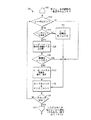
図3は、レーザ・モニタ及びシステム・モニタ・オペレーション・コード・モジュールに関連したタスクの実行に優先順位を付けて、図2に例示の光トランシーバ・モジュール30の動作を制御するため、マイクロコントローラ30によって用いられるプロセスの典型的な実施態様の1つを例示した流れ図100である。プロセス100は、モジュール較正/初期化の完了後、ステップ102から開始される。プロセス100は、次に、ステップ110において、レーザ・モニタ・オペレーション・コード・モジュールに進み、レーザ72の動作がモニタされ、制御される。ステップ110のレーザ・モニタ・オペレーション・コード・モジュールには、レーザ72の光出力パワー・レベルをモニタして、出力パワーを所望の目標値にほぼ等しいレベルに維持するため、必要に応じて、レーザ・バイアス電流制御回路76によってレーザ72に供給されるバイアス電流を調整する複数のタスクが含まれている。
FIG. 3 illustrates a
ステップ110におけるレーザ・モニタ・オペレーション・コード・モジュールには、さらに、111で表示の、レーザ72を初期化するための複数のタスクが含まれている。レーザ初期化には、レーザ72をパワー・オフ状態から所望の目標出力パワー・レベルにするためのタスクの実行が必要とされる。レーザ72の初期化を制御するためのタスクは、一般に、他のレーザ・モニタ・オペレーション・コード・モジュール・タスク程の頻度では実行されない。一般に、レーザ初期化を制御するタスクは、トランシーバ・モジュール30の初期起動後か、または、システムの障害によってレーザ72の停止及び再初期化が必要になった後に限って実行される。以下では、レーザ初期化111に関連したタスクを含む、ステップ110におけるレーザ・モニタ・オペレーション・コード・モジュールに関連したタスクの実行についてさらに詳述することにする。
The laser monitor operation code module at
マイクロコントローラ36が、ステップ110におけるレーザ・モニタ・オペレーション・コード・モジュールに関連した複数のタスクを実行すると、プロセス100は、ステップ112に移行し、レーザ・モニタ・ループ・カウンタが、値1だけインクリメントされる。プロセス100は、次に、ステップ114に進み、マイクロコントローラ36は、ループ・カウンタがしきい値に等しいか否かを問い合わせる。実施態様の1つでは、レーザ・モニタ・ループ・カウンタに関するしきい値は8である。プロセス100のステップ114において、ループ・カウンタのしきい値が「8」であることが示されるが、この値は、レーザ・モニタ・オペレーション・コード・モジュール・タスクに割り当てることが要求されるCPU60処理時間量に応じて、増/減可能である。ステップ114において、ループ・カウンタの値が8未満の場合、プロセス100は、ステップ110に戻り、マイクロコントローラ36は、再び、レーザ・モニタ・オペレーション・コード・モジュールの複数のタスクを実行する。ループ・カウンタの値が8の場合、マイクロコントローラ36は、レーザ72が十分に安定しているものと判断し、プロセス100は、ステップ116に進んで、システム・モニタ・オペレーション・コード・モジュールに関連した複数のタスクが実施される。
When the
ステップ116におけるシステム・モニタ・オペレーション・コード・モジュールには、光トランシーバ・モジュール30の動作を制御するのに役立つシステム動作パラメータをモニタして、調整するための複数のタスクが含まれている。さまざまな値をモニタして、調整するが、タスクは、主として、環境条件、及び、システム・エラーの補正に関して光トランシーバ・モジュール30のシステム動作パラメータを調整することに関連したものである。マイクロコントローラ36は、システム・モニタ・オペレーション・コード・モジュールの少なくとも1つのタスクを実行すると、レーザ・モニタ・ループ・カウンタを0にセットし、プロセス100は、ステップ110に戻り、もう一度、レーザ72をモニタするタスクの実行を開始する。ステップ116において行われるシステム・モニタ・オペレーション・コード・モジュール・タスクの実行については、さらに詳細に後述することにする。
The system monitor operation code module at
割り込み・オペレーション・コード・モジュール118には、マイクロコントローラ36がさまざまな送信元から受信するさまざまなタイプの割り込み信号に応答して実行される、複数のタスクを制御するための複数のタスク・コード・モジュールが含まれている。マイクロコントローラ36は、割り込み信号に応答して、まず、レーザ及びシステム・モニタ・タスクの優先順位付けされたプロセスを中断し、受信した割り込み信号のタイプを判定する。割り込み信号のタイプに応じて、マイクロコントローラ36は、対応する複数のタスク・コード・モジュールをすぐに実行してから、レーザ及びシステム・モニタ・タスクの優先順位付けされたプロセスを再開するか、あるいは、割り当てられた優先レベルに基づいて、他のタスク・コード・モジュールと共に前記複数のタスク・コード・モジュールを実行する。割り込みモジュール118については、さらに詳細に後述する。
The interrupt
図3の流れ図100には、システム・モニタ・タスクに関連したタスクと対照して、レーザ72のモニタに関連したタスクを実施するため、マイクロコントローラ36によって付与された優先順位が例示されている。従って、流れ図100は、レーザ72によって送り出される光出力信号のパワーをモニタし、制御する操作のクリティカルな特性を反映している。レーザ・モニタ・ループ・カウンタの値が8の場合、レーザ・モニタ・オペレーション・コード・モジュールに関連したタスクは、システム・モニタ・オペレーション・コード・モジュールに関連したタスクが1回実行される毎に、8回実行される。
The
図4は、図3のステップ112及び114で概略を説明した、レーザ72をモニタするためのプロセス120の典型的な実施態様の1つを例示した流れ図である。プロセス120は、光トランシーバ・モジュール30の較正及び初期化が完了した後、ステップ102から開始される。プロセス120は、次に、ステップ122に進み、マイクロコントローラ36が、レーザ72がオンか否かを問い合わせる。ステップ122の問い合わせに対する返答が「はい」の場合、プロセス120はステップ124に進む。
FIG. 4 is a flowchart illustrating one exemplary embodiment of a
ステップ124において、マイクロコントローラ36は、レーザ72の出力パワーが安定しているか否かを判定する。マイクロコントローラ36は、レーザ出力パワー検知回路74から、レーザ72の現在の出力パワー・レベル表した値を読み取る。マイクロコントローラ36は、次に、レーザ72の現在の出力パワー・レベルを表す値と、メモリ・ブロック62に記憶されているレーザ72の目標出力パワー・レンジとを比較する。現在の出力パワーを表す値が、目標出力パワー・レンジ内になければ、プロセス120は、ステップ111におけるレーザ初期化モジュールに進む。上述のように、レーザ初期化には、できるだけ速く、レーザ72をパワー・オフ状態から所望のレンジ内のパワー・レベルを有する出力信号を送り出せる状態にするための複数のタスクを実行することが必要になる。レーザ72の初期化については、さらに詳細に後述する。レーザ72は、ステップ111で初期化されると、プロセス120はステップ112に進む。
In
ステップ124におけるレーザ72の現在の出力パワーを表す値が、メモリ・ブロック62に記憶されている目標レンジ内である場合、プロセス120は、ステップ126に進む。ステップ126において、マイクロコントローラ36は、レーザ・バイアス電流が所望の目標レンジ内であるか否かを判定する。マイクロコントローラ36は、レーザ・バイアス電流検知回路75から、レーザ72の現在のバイアス電流レベルを表わす値を読み取って、現実の値に変換する。マイクロコントローラ36は、次に、現在のバイアス電流の現実の値とメモリ・ブロック62に記憶されている目標バイアス電流目標レンジとを比較する。現在のバイアス電流レベルが所望の目標レンジ内であれば、プロセス120は、ステップ112に進む。
If the value representing the current output power of
現在のバイアス電流レベルが、所望の目標レンジ内になければ、プロセス120は、ステップ130に進む。バイアス電流レベルが、所望の目標レンジ未満であれば、マイクロコントローラ36は、レーザ・バイアス電流制御回路76が、所定の増分量だけレーザ・バイアス電流を増大させるようにする。バイアス電流レベルが、所望の目標レンジを超えていると、マイクロコントローラ36は、レーザ・バイアス電流制御回路76が、所定の増分量だけレーザ・バイアス電流を減少させるようにする。バイアス電流の増/減後、プロセス120はステップ112に進む。
If the current bias current level is not within the desired target range,
ステップ112において、マイクロコントローラ36は、レーザ・モニタ・ループ・カウンタを値1だけインクリメントする。次に、プロセス120は、ステップ114に進み、マイクロコントローラ36は、ループ・カウンタの値が8か否かを問い合わせる。前述のように、プロセス120において、ループ・カウンタのしきい値が8であることが示されるが、この値は、レーザ・モニタに割り当てることが要求されるCPU60処理時間量に応じて、増/減可能である。モニタ・ループ・カウンタの値が8未満の場合、プロセス120は、ステップ122に戻り、レーザ72のモニタリングに関連したタスクの実行を続ける。モニタ・ループ・カウンタの値が8の場合、レーザ72は、十分に安定しているとみなされ、プロセス120は、ステップ132に進み、その時点において、システム・モニタ・オペレーション・コード・モジュールに関連したタスクが実行されることになる。
At
図5は、本発明による光トランシーバ30に関するシステム・モニタ・プロセス140の典型的な実施態様の1つを例示した流れ図である。システム・モニタには、主として、環境の変化に関するさまざまなトランシーバ・モジュール30の動作パラメータをモニタして、調整し、システム・エラーを補正し、保守を行うための複数のタスク・コード・モジュールが含まれている。実施態様の1つでは、複数のシステム・モニタ・タスク・コード・モジュールは、細分されて、3つのグループを形成しており、第1のグループは、第1の優先レベルが割り当てられ、第2のグループは、第2の優先レベルが割り当てられ、第3のグループは、第3の優先レベルが割り当てられているが、第1のグループに含まれるタスク・コード・モジュールは、優先順位が最高とみなされ、第3のグループのタスク・コード・モジュールは、優先順位が最低とみなされる。
FIG. 5 is a flowchart illustrating one exemplary embodiment of a
システム・モニタ・プロセス140は、レーザ・モニタ・プロセス120のようなレーザ・モニタ・プロセスによって、マイクロコントローラ36が、レーザ72の働きを危うくすることなく、CPU60の処理時間をもっぱらシステム・モニタ・タスクに充てるのに十分なほど、レーザ72が安定しているものとみなされると、ステップ132から開始される。プロセス140は、次に、ステップ142に進み、マイクロコントローラ36は、第1のグループをなすモニタ・タスクから各タスク・コード・モジュールを実行する。第1のグループ内のタスク・コード・モジュールによって実施されるタスク例には、システム温度に基づいてレーザ72の出力変調を調整すること、及び、レーザ72の出力パワーをモニタして、目の防護のために停止できるように、アラームをセットすることがある。
The
第1のグループのグループをなすタスク・コード・モジュールが、全て、実行されると、プロセス140は、ステップ144に進み、マイクロコントローラ36が、第2のグループからのタスク・コード・モジュールの1つを実行する。第2のグループ内のタスク・コード・モジュールによって実施されるタスク例には、レーザ出力パワーの温度調整、及び、送信機の供給電圧障害設定のモニタがある。実施態様の1つでは、マイクロコントローラ36は、第2のグループからのタスク・コード・モジュールの循環リストを保守し、どのタスク・コード・モジュールが最後に実行されたかを監視する。循環リストの最後のタスク・コード・モジュールが実行されると、マイクロコントローラは、循環リストの最初のタスク・コード・モジュールに戻る。
When all the task code modules of the first group have been executed, the
第2グループからのタスク・コード・モジュールの1つを実行すると、プロセス140は、ステップ146に進み、システム・モニタ・ループ・カウンタが、値1だけインクリメントされる。プロセス140は、次に、ステップ148に進み、マイクロコントローラ36は、システム・モニタ・ループ・カウンタ値が所定のしきい値に等しいか否かを問い合わせる。実施態様の1つでは、システム・モニタ・ループ・カウンタのしきい値は、2である。プロセス140のステップ148において、システム・モニタ・ループ・カウンタの値が2であると示されるが、この値は、第3グループからのシステム・モニタ・タスク・コード・モジュールの実行に、CPU60の処理時間をどれだけ充てるように要求されるかに応じて、増/減可能である。
Upon executing one of the task code modules from the second group, the
システム・モニタ・ループ・カウンタ値が2未満の場合、プロセス140はステップ152に進む。システム・モニタ・ループ・カウンタ値が2の場合、プロセス140はステップ150に進み、マイクロコントローラ36は、第3グループからのシステム・モニタ・タスク・コード・モジュールの1つを実行する。第3グループ内のタスク・コード・モジュールによって実施されるタスク例には、アラーム及び警告フラグのセッティング及びクリアがある。実施態様の1つでは、マイクロコントローラ36は、第3グループからのタスク・コード・モジュールの循環リストを保守し、どのタスク・コード・モジュールが最後に実行されたかを監視する。循環リストの最後のタスク・コード・モジュールが実行されると、マイクロコントローラは、循環リストの最初のタスク・コード・モジュールに戻る。
If the system monitor loop counter value is less than two,
第3グループからのタスク・コード・モジュールの1つを実行すると、マイクロコントローラ36は、システム・モニタ・ループ・カウンタの値を0にセットし、プロセス140は、ステップ152に進む。ステップ152において、プロセス140は、レーザ・モニタ・プロセス120のようなレーザ・モニタ・プロセスに進む。
Upon executing one of the task code modules from the third group, the
118における割り込み・オペレーション・コード・モジュールには、さまざまな送信元から受信するさまざまなタイプの割り込み信号に応答して実行される、複数のタスクを制御するための複数のタスク・コード・モジュールが含まれている。割り込み信号には複数のタイプがあり、割り込み信号のタイプに基づいて優先レベルが割り当てられた割り込み信号に応答して実行されるタスクを制御するためのタスク・コード・モジュールが設けられている。実施態様の1つでは、割り込み信号は、第1のタイプまたは第2のタイプである。 The interrupt operation code modules at 118 include multiple task code modules for controlling multiple tasks that are executed in response to various types of interrupt signals received from various sources. Have been. There are a plurality of types of interrupt signals, and a task code module for controlling a task executed in response to the interrupt signal assigned a priority level based on the type of the interrupt signal is provided. In one embodiment, the interrupt signal is of a first type or a second type.
割り込み信号の受信に応答して、マイクロコントローラ36は、まず、レーザ及びシステム・モニタ・タスク優先順位のプロセスを中断し、受信した割り込み信号のタイプを判定する。割り込み信号が第1のタイプであれば、マイクロコントローラ36は、対応する複数のタスク・コード・モジュールをすぐに実行してから、レーザ及びシステム・モニタ・タスク優先順位のプロセスを再開する。第1のタイプの割り込み信号の例には、レーザ発光禁止信号及び故障信号がある。
In response to receiving the interrupt signal,
割り込み信号が第2のタイプであれば、マイクロコントローラ36は、レーザ及びシステム・モニタ・タスク優先順位のプロセス内における適正な位置に、対応する複数のタスク・コード・モジュールを配置して、その後、割り込み信号に関連した複数のタスクが、割り当てられた優先レベルに基づいて、他のタスク・コード・モジュールと共に実行される、優先順位付けプロセスを再開する。第2のタイプの割り込み信号例には、メモリにデータを書き込むホスト要求がある。
If the interrupt signal is of the second type, the
良質の光トランシーバ・モジュールが得られるようにするため、完璧に実施しなければならないタスクの1つは、レーザを始動させる、すなわち初期化することである。レーザの初期化には、できるだけ速く、レーザ72をパワー・オフ状態から目標レンジ内のパワー・レベルを備えた出力信号を送り出せる状態にするための複数のタスクを実行することが必要になる。レーザ初期化は、一般に、トランシーバ・モジュール30の起動後、または、トランシーバのシステム障害の後または発光禁止(ディゼイブル)の解除後に実施される。
One of the tasks that must be performed perfectly to get a good quality optical transceiver module is to start, or initialize, the laser. Initializing the laser requires performing as many tasks as possible to bring the
図6Aは、本発明に従ってレーザ72を初期化するためのプロセス160の典型的な実施態様の1つを例示した流れ図である。初期化プロセス160は、例えば、図4に例示のレーザ・モニタ・プロセス120のステップ124におけるように、レーザ・モニタ・プロセスで、レーザ72の出力パワーが安定していないと判定されると、ステップ162から開始される。プロセス160は、次に、ステップ164に進み、マイクロコントローラ36によって、メモリ・ブロック62からレーザ・バイアス電流シード値が読み取られる。シード値は、メーカにおいて、出力パワー・レベルが所望の出力パワー・レベル目標レンジ内の光出力信号をレーザ72から生じさせることになった、レーザ・バイアス電流の値である。マイクロコントローラ36は、シード値をレーザ・バイアス電流制御回路76に記憶しておき、レーザ・バイアス電流制御回路76によって、シード値にほぼ等しい(シード値にほぼ対応する)値のバイアス電流(IBIAS)によるバイアスがレーザ72にかけられるようにする。
FIG. 6A is a flowchart illustrating one exemplary embodiment of a
プロセス160は、次に、ステップ166に進み、マイクロコントローラ36によって、光出力信号モニタ電流(IMON)の値がレーザ出力パワー検知回路74から読み取られる。実施態様の1つにおいて、レーザ出力パワー検知回路74には、レーザ72によって送り出される光出力信号をサンプリングして、レーザ72の光出力パワーを表す値を有するIMON電流レベルを生じるフォトダイオードが含まれている。
The
プロセス160は、次に、ステップ168に進み、マイクロコントローラ36によって、ステップ166からのIMON値とメモリ・ブロック62に記憶されているIMONの所望の目標レンジが比較される。IMON値が所望のレンジ内である場合、プロセス160は、ステップ170に進み、レーザ・モニタ・プロセス120のステップ112に進む。IMON値が所望のレンジ内にない場合、プロセス160はステップ172に進む。
The
ステップ172において、マイクロコントローラは、レーザ・バイアス電流制御回路76に、メモリ・ブロック62に記憶されている一定値(K)だけレーザ・バイアス電流をインクリメントさせることによって、レーザ72にインクリメントされたバイアス電流(IBIAS′)がかかるようにする。プロセス160は、次に、ステップ174に進み、マイクロコントローラ36によって、レーザ72にIBIAS′によるバイアスがかかった後、レーザ出力パワー検知回路74から送り出される光出力信号モニタ電流の値が読み取られる。光出力信号モニタ電流に関する新しい値は、IMON′と呼ばれる。
In
プロセス160は、次に、ステップ176に進み、マイクロコントローラ36によって、IBIAS、IMON、IBIAS′、及び、IMON′を用いた数学的な外挿が実施され、結果として、所望の目標レンジ内の出力信号モニタ電流(IMON)が得られることになる、出力パワー・レベルを備えた光出力信号をレーザ72から生じさせる、レーザ・バイアス電流の所望のレベルが計算される。プロセス160は、次に、ステップ178に進み、マイクロコントローラ36は、レーザ・バイアス電流に関する計算値をレーザ・バイアス電流制御回路76に記憶する。レーザ・バイアス電流制御回路76は、次に、計算されたバイアス電流によってレーザ72にバイアスをかけ、レーザ72がほぼ所望のレンジ内の出力パワー・レベルを備えた光出力信号を送り出すようにする。
The
図6Bは、本発明に従ってレーザ72を初期化するプロセス180の典型的な実施態様の1つを例示した流れ図である。プロセス180は、例えば、図4に例示のレーザ・モニタ・プロセス120のステップ124におけるように、レーザ・モニタ・プロセスで、レーザ72の出力パワーが安定していないと判定されると、ステップ182から開始される。プロセス180は、次に、ステップ184に進み、マイクロコントローラ36によって、メモリ・ブロック62からレーザ・バイアス電流のシード値が読み取られる。シード値は、メーカにおいて、出力パワー・レベルが所望の出力パワー・レベル目標レンジ内の光出力信号をレーザ72から生じさせることになった、レーザ・バイアス電流の値である。マイクロコントローラ36は、シード値をレーザ・バイアス電流制御回路76に記憶しておき、レーザ・バイアス電流制御回路76によって、シード値にほぼ等しい(シード値にほぼ対応する)値のバイアス電流(IBIAS)によるバイアスがレーザ72にかけられるようにする。
FIG. 6B is a flowchart illustrating one exemplary embodiment of a
プロセス180は、次に、ステップ186に進み、マイクロコントローラ36によって、光出力信号モニタ電流(IMON)の値がレーザ出力パワー検知回路74から読み取られる。実施態様の1つにおいて、レーザ出力パワー検知回路74には、レーザ72によって送り出される光出力信号をサンプリングして、レーザ72の光出力パワーを表す値を有するIMON電流レベルを生じるフォトダイオードが含まれている。
The
プロセス180は、次に、ステップ188に進み、マイクロコントローラ36によって、ステップ186において読み取られたIMONとメモリ・ブロック62に記憶されているIMONに関する所望の目標値(ITARGET)との差(Δ)が求められる。プロセス180は、次に、ステップ190に進み、マイクロコントローラ36は、メモリ・ブロック62に記憶されるルックアップ・テーブルの索引としてΔ値を利用する。ルックアップ・テーブルには、レーザ72が所望のレンジ内の出力パワー・レベルを備えた光出力信号を生じるようにするため、IBIASに加えなければならないΔ値に基づいた、所定の増分電流値(IINC)の索引が納められている。
The
プロセス180は、次に、ステップ192に進み、IINCの絶対値がメモリ・ブロック62に記憶されている所望の値(θ)と比較される。IINCの絶対値がθ未満の場合、プロセス180は、ステップ194に進み、図4に例示されたレーザ・モニタ・プロセス120のステップ112に出る。IINCの絶対値がθ以上の場合、プロセス180はステップ196に進む。ステップ196において、マイクロコントローラ36は、IBIASに増分電流値IINCを加え、IBIASのこの調整値をレーザ・バイアス電流制御回路76に記憶する。次に、レーザ・バイアス電流制御回路76は、結果として、レーザ72からほぼ所望のレンジ内の出力パワー・レベルを備えた光出力信号が生じさせることになる、IBIASの調整値にほぼ等しい値のバイアス電流によってレーザ72にバイアスをかける。
The
図6Cは、本発明に従ってレーザ72を初期化するプロセス200の典型的な実施態様の1つを例示した流れ図である。プロセス200は、例えば、図4に例示のレーザ・モニタ・プロセス120のステップ124におけるように、レーザ・モニタ・プロセスで、レーザ72の出力パワーが安定していないと判定されると、ステップ202から開始される。プロセス200は、次に、ステップ204に進み、マイクロコントローラ36によって、メモリ・ブロック62からレーザ・バイアス電流シード値が読み取られる。シード値は、メーカにおいて、出力パワー・レベルが所望の出力パワー・レベル目標レンジ内の光出力信号をレーザ72から生じさせることになった、レーザ・バイアス電流の値である。マイクロコントローラ36は、シード値をレーザ・バイアス電流制御回路76に記憶しておき、レーザ・バイアス電流制御回路76によって、シード値にほぼ等しい(シード値にほぼ対応した)値のバイアス電流(IBIAS)によるバイアスがレーザ72にかけられるようにする。
FIG. 6C is a flowchart illustrating one exemplary embodiment of a
プロセス200は、次に、ステップ206に進み、マイクロコントローラ36によって、レーザ出力パワー検知回路74から光出力信号モニタ電流(IMON)の値が読み取られる。実施態様の1つにおいて、レーザ出力パワー検知回路74には、レーザ72から送り出される光出力信号をサンプリングして、レーザ72の光出力パワーを表す値を有するIMON電流レベルを生じるフォトダイオードが含まれている。
The
プロセス200は、次に、ステップ208に進み、マイクロコントローラ36は、ステップ206において読み取られるIMONとメモリ・ブロック62に記憶されているIMONの所望の目標値(ITARGET)との差(Δ)を求め、次に、Δ値に、やはりメモリ・ブロック62に記憶されている利得値(ゲイン)を掛けて、調整Δ値=(IMON−ITARGET)×(利得値)を生成する。
The
プロセス200は、次に、ステップ210に進み、調整Δ値の絶対値がメモリ・ブロック62に記憶されている所望の値(θ)と比較される。調整Δ値の絶対値がθ未満の場合、プロセス200は、ステップ212に進み、図4に例示されたレーザ・モニタ・プロセス120のステップ112に進む。調整Δ値の絶対値がθ以上の場合、プロセス200はステップ214に進む。ステップ214において、マイクロコントローラ36は、IBIASから調整Δ値を引き、IBIASのこの調整値をレーザ・バイアス制御回路76に記憶する。次に、バイアス電流制御回路76は、結果として、ほぼ所望のレンジ内の出力パワー・レベルを備えた光出力信号がレーザ72から生じさせることになる、IBIASの調整値にほぼ等しい値のバイアス電流によってレーザ72にバイアスをかける。
The
図6Dは、本発明に従ってレーザ72を初期化するプロセス220の典型的な実施態様の1つを例示した流れ図である。プロセス220は、例えば、図4に例示のレーザ・モニタ・プロセス120のステップ124におけるように、レーザ・モニタ・プロセスで、レーザ72の出力パワーが安定していないと判定されると、ステップ222から開始される。プロセス200は、次に、ステップ224に進み、マイクロコントローラ36によって、メモリ・ブロック62からレーザ・バイアス電流シード値が読み取られる。シード値は、メーカにおいて、出力パワー・レベルが所望の出力パワー・レベル目標レンジ内の光出力信号をレーザ72から生じさせることになった、レーザ・バイアス電流に対応する値である。マイクロコントローラ36は、シード値をレーザ・バイアス電流制御回路76に記憶しておき、制御回路76によって、シード値にほぼ等しい(シード値にほぼ対応する)値のバイアス電流(IBIAS)によるバイアスがレーザ72にかけられるようにする。
FIG. 6D is a flowchart illustrating one exemplary embodiment of a
プロセス220は、次に、ステップ226に進み、マイクロコントローラ36によって、レーザ出力パワー検知回路74から光出力信号モニタ電流(IMON)の値が読み取られる。実施態様の1つにおいて、レーザ出力パワー検知回路74には、レーザ72から送り出される光出力信号をサンプリングして、レーザ72の光出力パワーを表す値を有するIMON電流レベルを生じるフォトダイオードが含まれている。プロセス220は、次に、ステップ228に進み、マイクロコントローラ36は、ステップ206において読み取られるIMONとメモリ・ブロック62に記憶されているIMONの所望の目標値(ITARGET)との差(Δ)を求める。プロセス220は、ステップ230に進み、Δの絶対値がメモリ・ブロック62に記憶されている所望の値(θ)と比較される。Δの絶対値がθ未満の場合、プロセス220は、ステップ232に進み、図4に例示のレーザ・モニタ・プロセス120のステップ112に進む。Δの絶対値がθ以上の場合、プロセス220は、ステップ234に進む。ステップ234では、マイクロコントローラ36によって、IMONとITARGETが比較される。
The
IMONがITARGET以下の場合、プロセス220はステップ236に進む。ステップ236において、マイクロコントローラ36は、メモリ・ブロック62に記憶されている所定の定数値(K)をIBIASに加えて、IBIASの調整値をレーザ・バイアス電流制御回路76に記憶する。次に、レーザ・バイアス電流制御回路76は、結果として、ほぼ所望のレンジ内の出力パワー・レベルを備えた光出力信号がレーザ72から生じさせることになる、IBIASの調整値にほぼ等しい値のバイアス電流によってレーザ72にバイアスをかける。
If I MON is less than or equal to I TARGET ,
IMONがITARGETを超えていると、プロセス220は、ステップ238に進む。ステップ238において、マイクロコントローラ36は、IBIASからメモリ・ブロック62に記憶されている所定の定数値(K)を引いて、IBIASの調整値をレーザ・バイアス制御回路76に記憶する。次に、バイアス電流制御回路76は、結果として、ほぼ所望のレンジ内の出力パワー・レベルを備えた光出力信号をレーザ72から生じさせることになる、IBIASの調整値にほぼ等しい値のバイアス電流によってレーザ72にバイアスをかける。
If I MON exceeds I TARGET ,
図6Eは、本発明に従ってレーザ72を初期化するプロセス240の典型的な実施態様の1つを例示した流れ図である。プロセス240は、例えば、図4に例示のレーザ・モニタ・プロセス120のステップ124におけるように、レーザ・モニタ・プロセスで、レーザ72の出力パワーが安定していないと判定されると、ステップ242から開始される。プロセス240は、次に、ステップ244に進み、マイクロコントローラ36によって、フラグ(F)が値0にセットされ、変数(K)が値10にセットされる。ステップ246では、マイクロコントローラ36によって、メモリ・ブロック62からレーザ・バイアス電流シード値が読み取られる。シード値は、メーカにおいて、出力パワー・レベルが所望の出力パワー・レベル目標レンジ内の光出力信号をレーザ72から生じさせることになった、レーザ・バイアス電流の値である。マイクロコントローラ36は、シード値をレーザ・バイアス電流制御回路76に記憶しておき、レーザ・バイアス電流制御回路76によって、シード値にほぼ等しい(シード値にほぼ対応する)値のバイアス電流(IBIAS)によるバイアスがレーザ72にかけられるようにする。
FIG. 6E is a flowchart illustrating one exemplary embodiment of a
プロセス240は、次に、ステップ248に進み、マイクロコントローラ36によって、レーザ出力パワー検知回路74から光出力信号モニタ電流(IMON)の値が読み取られる。実施態様の1つにおいて、レーザ出力パワー検知回路74には、レーザ72から送り出される光出力信号をサンプリングして、レーザ72の光出力パワーを表した値を有するIMON電流レベルを生じるフォトダイオードが含まれている。ステップ250において、マイクロコントローラ36は、ステップ206において読み取られるIMONとメモリ・ブロック62に記憶されているIMONの所望の目標値(ITARGET)との差(Δ)を求める。
The
プロセス240は、次に、ステップ252に進み、マイクロコントローラ36は、フラグ(F)が0に等しいか否かを問い合わせる。返答が「いいえ」の場合、プロセス240は、ステップ254に進む。返答が「はい」の場合、プロセス240は、ステップ256に進み、マイクロコントローラ36によって、フラグ(F)の値が値1にセットされ、変数(Δ′)の値は差Δに等しい値にセットされる。
ステップ254では、マイクロコントローラ36は、差Δの符号が変数Δ′の符号と同じか否かを問い合わせる。返答が「はい」の場合、プロセス240はステップ258に進む。返答が「いいえ」の場合、プロセス240はステップ260に進み、マイクロコントローラ36によって、変数Kが値1にセットされる。
In
ステップ258では、マイクロコントローラ36は、Δの絶対値がメモリ・ブロック62に記憶されている所望の値(θ)に比べて小さいか否かを問い合わせる。Δの絶対値がθ未満の場合、プロセス240はステップ262に進み、図4に例示されたレーザ・モニタ・プロセス120のステップ112に出る。Δの絶対値がθ以上の場合、プロセス240はステップ264に進む。
In
ステップ264では、マイクロコントローラ36は、差Δが値0を超えるか否かを問い合わせる。Δが0以下の場合、プロセス240はステップ266に進み、マイクロコントローラ36は、IBIASに変数Kの値を加えて、レーザ・バイアス制御回路76にIBIASのこの調整値を記憶してステップ248に戻る。Δが0を超えていると、プロセス240はステップ268に進み、マイクロコントローラ36は、IBIASから変数Kの値を引き、IBIASのこの調整値をレーザ・バイアス制御回路76に記憶する。次に、レーザ・バイアス制御回路76は、IBIASの調整値にほぼ等しい値のバイアス電流によってレーザ72にバイアスをかけ、プロセス240はステップ248に戻る。
In
レーザ72のようなレーザを利用することに関する利点の1つは、とりわけ、光信号が光ファイバ42のようなコアの小さい光ファイバに送り込まれる場合に、発光ダイオード(LED)または他の発光素子よりもはるかに高いパワー・レベルの光出力信号が得られるという点である。欠点の1つは、レーザの光出力パワーが温度依存性であるという点である。例えば、レーザにある設定値のバイアス電流によってバイアスをかけると、第1の温度で第1のパワー・レベルの光信号を生じ、第2の温度で第2のパワー・レベルの光信号を生じることになる。
One of the advantages associated with utilizing a laser, such as
これを考慮して、メモリ・ブロック62に記憶されるレーザ・バイアス電流シード値を改善する方法の1つは、光トランシーバ・モジュールの製造及びテスト時に生じた温度値において、レーザ72からパワー・レベルが所望のレンジ内の光信号を生じさせることになったバイアス電流値にすることである。レーザ72の初期化時における光トランシーバ30の温度が、製造時の温度と一致する確率は低い。従って、それぞれ、図6A、6B、6C、6D、6Eに例示されたレーザ初期化プロセス160、180、200、220、及び、240を改善する方法の1つは、温度検知回路78によって得られるレーザ72の初期化時における温度の現在値を利用して、メモリ・ブロック62に記憶されているレーザ・バイアス電流シード値を調整しておいてから、レーザ・バイアス電流制御回路76に記憶することである。
With this in mind, one way to improve the laser bias current seed value stored in the memory block 62 is to use the power level from the
図6Fは、初期化時に、レーザ72から所望のレンジにより近い光信号を生じさせることになるレーザ・バイアス電流が得られるようにするため、光トランシーバ・モジュール30の温度に基づいて、メモリ・ブロック62に記憶されているレーザ・バイアス・シード値を調整するプロセス270の典型的な実施態様の1つを例示した流れ図である。プロセス270は、レーザ初期化プロセス160、180、200、220、及び、240の、それぞれ、ステップ164、184、204、224、及び、246に置き換えられる。
FIG. 6F shows the memory block based on the temperature of the
プロセス270は、例えば、図4に例示のレーザ・モニタ・プロセス120のステップ124におけるように、レーザ・モニタ・プロセスで、レーザ72の出力パワーが安定していないと判定されると、ステップ272から開始される。プロセス270は、次に、ステップ274に進み、マイクロコントローラ36によって、メモリ・ブロック62からレーザ・バイアス電流シード値(IBIAS)が読み取られる。プロセス270は、次に、ステップ276に進み、マイクロコントローラ36によって、温度検知回路78から、レーザ72の現在の温度を表す温度値(TEMP)が読み取られる。
The
プロセス270は、次に、ステップ278に進み、マイクロコントローラ36によって、IBIASのシード値に、現在のレーザ温度(TEMP)とメモリ・ブロック62に記憶されている温度定数(TEMPCO)との積を加えた値に等しい、IBIASに関する温度調整値が求められる。プロセス270は、次に、ステップ280に進み、マイクロコントローラ36は、IBIASに関する温度調整値をレーザ・バイアス電流制御回路76に記憶する。次に、レーザ・バイアス電流制御回路76は、IBIASの温度調整値(温度を加味した調整値)によってレーザ72にバイアスをかける。
The
結論として、レーザ初期化時に生じる実際の温度を考慮して、製造時にトランシーバ・モジュールに記憶された初期化レーザ・バイアス電流値を調整することによって、本発明によるトランシーバ・モジュール30は、レーザを初期化すると、所望のパワー・レンジ内にある光出力信号をより迅速かつ正確に送り出すことが可能になる。さらに、レーザ・バイアス電流のインクリメント及びデクリメントを繰り返す従来の技法とは対照的に、外挿技法及びルックアップ・テーブルを用いて、所望の出力レンジ内にある出力信号を生じることになるレーザ・バイアス電流を直接求めることによって、レーザの初期化に要する時間をさらに短縮することが可能になる。
In conclusion, by adjusting the initialization laser bias current value stored in the transceiver module during manufacture to account for the actual temperature that occurs during laser initialization,
望ましい実施態様について明らかにするため、本明細書では、特定の実施態様について例示し、解説してきたが、通常の当業者であれば明らかなように、本発明の範囲を逸脱することなく、図示及び解説の特定の実施態様の代わりに、同じ目的を実現するように意図された、多種多様な代替及び/または同等実施例を用いることが可能である。化学、機械、電気機械、電気、及び、コンピュータ分野の当業者にはすぐに明らかになるように、本発明は、極めて多種多様な実施態様で実施することが可能である。本願は、本明細書に論述した好ましい実施態様のいかなる改変または変更も対象とすることを意図したものである。従って、本発明は、明らかに、特許請求の範囲及びその同等物のみによって制限されることを意図したものである。 While certain embodiments have been illustrated and described herein in order to illustrate preferred embodiments, it will be apparent to one skilled in the art that the drawings may be modified without departing from the scope of the invention. Instead of the specific embodiments described and described, it is possible to use a wide variety of alternative and / or equivalent embodiments intended to achieve the same purpose. The present invention can be implemented in a very wide variety of embodiments, as will be readily apparent to those skilled in the chemical, mechanical, electromechanical, electrical, and computer arts. This application is intended to cover any adaptations or variations of the preferred embodiments discussed herein. Accordingly, it is manifestly intended that this invention be limited only by the claims and the equivalents thereof.
なお、本発明は例として次の態様を含む。( )内の数字は添付図面の参照符号に対応する。
[1] バイアス電流に基づくパワー・レベルを有する光出力信号(42)を発生するように構成されたレーザ(72)と、
前記レーザに初期バイアス電流によるバイアスをかけ、前記パワー・レベルを表すモニタ信号を受信し、前記パワー・レベルと所望のパワー・レベル・レンジを比較して、前記パワー・レベルが前記所望のパワー・レベル・レンジ内になければ、前記レーザに調整されたバイアス電流によるバイアスをかけるように構成されたコントローラ(36)とを備えることを特徴とする、
光トランシーバ・モジュール(30)。
[2] 前記モニタ信号を生成するように構成されたセンサをさらに備えることを特徴とする、上記[1]に記載の光トランシーバ・モジュール。
[3] 光トランシーバ・モジュール(30)のレーザ(72)を初期化する方法であって、
前記レーザを用いて、バイアス電流に基づくパワー・レベルを有する光出力信号(42)を発生するステップと、
初期バイアス電流によって前記レーザにバイアスをかけるステップと、
前記パワー・レベルを表すモニタ信号を受信するステップと、
前記パワー・レベルと所望のパワー・レベル・レンジを比較するステップと、
前記パワー・レベルが前記所望のパワー・レベル・レンジ内になければ、前記レーザに調整されたバイアス電流によるバイアスをかけるステップとを有することを特徴とする方法。
[4] 光トランシーバ・モジュール(30)のレーザ(72)におけるレーザ・バイアス電流を設定する方法であって、
前記レーザ・バイアス電流を第1の値に設定するステップと、
前記レーザ・バイアス電流を前記第1の値にした場合の、第1のレーザ・モニタ電流を測定するステップと、
前記第1のレーザ・モニタ電流とレーザ目標電流との差(Δ)を求めるステップと、
前記レーザ・バイアス電流をΔに基づく調整値に設定するステップを有する、
方法。
[5] 前記レーザ・バイアス電流を前記調整値にした場合の、第2のレーザ・モニタ電流を測定するステップと、
前記第2のレーザ・モニタ電流と前記レーザ目標電流との第2の差(Δ2)を求めるステップと、
前記レーザ・バイアス電流をΔ2に基づく新しい調整値に設定するステップとをさらに有することを特徴とする上記[4]に記載の方法。
[6] ルックアップ・テーブルにΔによる索引付けをして、バイアス電流変数が得られるようにするステップと、
前記レーザ・バイアス電流を前記バイアス電流変数に基づく調整値に設定するステップとをさらに有することを特徴とする上記[4]に記載の方法。
[7] ルックアップ・テーブルにΔによる索引付けをして、バイアス電流変数が得られるようにするステップと、
前記バイアス電流変数を評価して、前記レーザ・バイアス電流を調整すべきか否かを判定するステップをさらに有することを特徴とする上記[4]に記載の方法。
[8] 利得とΔとの乗算をするステップと、
前記レーザ・バイアス電流を、前記利得とΔとを乗算した値に基づく調整値に設定するステップをさらに有することを特徴とする上記[4]に記載の方法。
[9] 利得とΔとを乗算するステップと、
前記利得とΔとを乗算した値を評価して、前記レーザ・バイアス電流を調整すべきか否かを判定するステップをさらに有することを特徴とする上記[4]に記載の方法。
[10] 前記第1のレーザ・モニタ電流が前記レーザ目標電流を超える場合には、前記レーザ・バイアス電流を前記第1の値未満の調整値に設定するステップと、
前記第1のレーザ・モニタ電流が前記レーザ目標電流未満の場合には、前記レーザ・バイアス電流を前記第1の値を超える調整値に設定するステップをさらに有することを特徴とする上記[4]に記載の方法。
[11] Δを評価して、前記レーザ・バイアス電流を調整すべきか否かを判定するステップをさらに有することを特徴とする上記[4]に記載の方法。
[12] Δを評価して、細分性の粗い調整と細分性の微細な調整のいずれかによって、前記レーザ・バイアス電流を調整すべきかを判定するステップをさらに有することを特徴とする上記[4]に記載の方法。
[13] 前記レーザ・バイアス電流を細分性の粗い調整による調整値に設定するステップをさらに有することを特徴とする上記[4]に記載の方法。
[14] 前記レーザ・バイアス電流を前記調整値にした場合の、第2のレーザ・モニタ電流を測定するステップと、
前記第2のレーザ・モニタ電流と前記レーザ目標電流との第2の差(Δ2)を求めるステップと、
前記レーザ・バイアス電流をΔ2に基づく、細分性の微細な調整による新しい調整値に設定するステップとをさらに有することを特徴とする上記[13]に記載の方法。
[15] 前記レーザ・バイアス電流を前記調整値にした場合の、第2のレーザ・モニタ電流を測定するステップと、
前記第2のレーザ・モニタ電流と前記レーザ目標電流との第2の差(Δ2)を求めるステップと、
Δ2の符号とΔの符号を比較するステップとをさらに有することを特徴とする上記[13]に記載の方法。
[16] 前記Δ2の符号が前記Δの符号と同じ場合には、前記レーザ・バイアス電流を細分性の粗い調整による新しい調整値に設定するステップと、
前記Δ2の符号が前記Δの符号と異なる場合には、前記レーザ・バイアス電流を細分性の微細な調整による新しい調整値に設定するステップをさらに有することを特徴とする上記[15]に記載の方法。
[17] Δの絶対値が所望の値を超える場合には、前記レーザ・バイアス電流を前記調整値に設定するステップをさらに有することを特徴とする上記[4]に記載の方法。
[18] Δが0を超える場合には、前記レーザ・バイアス電流を前記第1の値未満の調整値に設定するステップと、
Δが0未満の場合には、前記レーザ・バイアス電流を前記第1の値を超える調整値に設定するステップとをさらに有することを特徴とする上記[17]に記載の方法。
[19] 光トランシーバ・モジュール(30)のレーザ(72)におけるレーザ・バイアス電流を設定する方法であって、
前記レーザ・バイアス電流を第1の値に設定するステップと、
前記レーザ・バイアス電流を前記第1の値にした場合の、第1のレーザ・モニタ電流を測定するステップと、
前記第1のレーザ・モニタ電流が所望のレンジ内にあるか否かを判定するステップと、
前記第1のレーザ・モニタ電流が所望のレンジ内にない場合、前記レーザ・バイアス電流を調整された値に設定するステップとを有することを特徴とする方法。
[20] 前記第1のレーザ・モニタ電流が所望のレンジ内にない場合、
前記レーザ・バイアス電流を前記第1の値に基づく第2の値に設定するステップと、
前記レーザ・バイアス電流を前記第2の値にした場合の、第2のレーザ・モニタ電流を測定するステップと、
前記第1の値、前記第1のレーザ・モニタ電流、前記第2の値、及び、前記第2のレーザ・モニタ電流に基づいて、前記レーザ・バイアス電流の第3の値を決定するステップと、
前記レーザ・バイアス電流を前記第3の値にほぼ等しい調整値に設定するステップとをさらに有することを特徴とする上記[19]に記載の方法。
[21] 前記レーザ・バイアス電流を前記調整値にした場合の、第2のレーザ・モニタ電流を測定するステップと、
前記第2のレーザ・モニタ電流が所望のレンジ内にあるか否かを判定するステップと、
前記第2のレーザ・モニタ電流が所望のレンジ内にない場合、前記レーザ・バイアス電流を新しく調整された値に設定するステップとをさらに有することを特徴とする上記[19]に記載の方法。
[22] 前記レーザ・バイアス電流を前記第1の値に設定する前に、現在の光トランシーバ・モジュールの温度を反映するように、前記レーザ・バイアス電流の前記第1の値を調整するステップをさらに有することを特徴とする上記[3]、[4]、または[19]に記載の方法。
The present invention includes the following aspects as examples. The numbers in parentheses correspond to the reference numerals in the attached drawings.
[1] a laser (72) configured to generate an optical output signal (42) having a power level based on a bias current;
Biasing the laser with an initial bias current, receiving a monitor signal representative of the power level, comparing the power level to a desired power level range, and determining that the power level is the desired power level; A controller (36) configured to bias the laser with the adjusted bias current if not within the level range.
Optical transceiver module (30).
[2] The optical transceiver module according to the above [1], further comprising a sensor configured to generate the monitor signal.
[3] A method for initializing a laser (72) of the optical transceiver module (30),
Using the laser to generate an optical output signal having a power level based on a bias current;
Biasing the laser with an initial bias current;
Receiving a monitor signal representative of the power level;
Comparing the power level with a desired power level range;
Biasing the laser with an adjusted bias current if the power level is not within the desired power level range.
[4] A method for setting a laser bias current in the laser (72) of the optical transceiver module (30),
Setting the laser bias current to a first value;
Measuring a first laser monitor current when the laser bias current is at the first value;
Determining the difference (Δ) between the first laser monitor current and the laser target current;
Setting the laser bias current to an adjustment value based on Δ,
Method.
[5] measuring a second laser monitor current when the laser bias current is set to the adjustment value;
Determining a second difference (Δ2) between the second laser monitor current and the laser target current;
Setting the laser bias current to a new adjustment value based on [Delta] 2.
[6] indexing the look-up table by Δ to obtain a bias current variable;
Setting the laser bias current to an adjustment value based on the bias current variable.
[7] indexing the look-up table by Δ to obtain a bias current variable;
The method of
[8] multiplying the gain by Δ;
The method according to [4], further comprising setting the laser bias current to an adjustment value based on a value obtained by multiplying the gain by Δ.
[9] multiplying the gain by Δ;
The method of
[10] setting the laser bias current to an adjustment value less than the first value when the first laser monitor current exceeds the laser target current;
When the first laser monitor current is less than the laser target current, the method further comprises the step of setting the laser bias current to an adjustment value exceeding the first value [4]. The method described in.
[11] The method according to the above [4], further comprising evaluating Δ to determine whether to adjust the laser bias current.
[12] The above-mentioned [4], further comprising the step of evaluating Δ to determine whether the laser bias current should be adjusted by coarse adjustment or fine adjustment. ].
[13] The method according to the above [4], further comprising the step of setting the laser bias current to an adjustment value by coarse adjustment.
[14] measuring a second laser monitor current when the laser bias current is set to the adjustment value;
Determining a second difference (Δ2) between the second laser monitor current and the laser target current;
Setting the laser bias current to a new adjustment value by fine adjustment of the granularity based on Δ2.
[15] measuring a second laser monitor current when the laser bias current is set to the adjustment value;
Determining a second difference (Δ2) between the second laser monitor current and the laser target current;
The method according to [13], further comprising comparing the sign of Δ2 with the sign of Δ.
[16] If the sign of Δ2 is the same as the sign of Δ, setting the laser bias current to a new adjustment value by coarse adjustment.
If the sign of Δ2 is different from the sign of Δ, the method further comprises the step of setting the laser bias current to a new adjustment value by fine adjustment of fineness. Method.
[17] The method according to the above [4], further comprising setting the laser bias current to the adjustment value when the absolute value of Δ exceeds a desired value.
[18] If Δ exceeds 0, setting the laser bias current to an adjustment value less than the first value;
Setting the laser bias current to an adjustment value greater than the first value if Δ is less than zero.
[19] A method for setting a laser bias current in a laser (72) of an optical transceiver module (30),
Setting the laser bias current to a first value;
Measuring a first laser monitor current when the laser bias current is at the first value;
Determining whether the first laser monitor current is within a desired range;
Setting the laser bias current to an adjusted value if the first laser monitor current is not within a desired range.
[20] If the first laser monitor current is not within a desired range,
Setting the laser bias current to a second value based on the first value;
Measuring a second laser monitor current when the laser bias current is at the second value;
Determining a third value of the laser bias current based on the first value, the first laser monitor current, the second value, and the second laser monitor current; ,
Setting the laser bias current to an adjustment value approximately equal to the third value.
[21] measuring a second laser monitor current when the laser bias current is set to the adjustment value;
Determining whether the second laser monitor current is within a desired range;
Setting the laser bias current to a newly adjusted value if the second laser monitor current is not within a desired range.
[22] adjusting the first value of the laser bias current to reflect a current temperature of the optical transceiver module before setting the laser bias current to the first value; The method according to the above [3], [4], or [19], further comprising:
30 光トランシーバ・モジュール
32 送信機
34 受信機
36 コントローラ(マイクロコントローラ)
40 発光素子
42、46 光ファイバ(光ファイバケーブル)
44 光検出素子
48 トランシーバ・オペレーション・コード
72 レーザ
74 レーザ出力パワー検知回路
40 light emitting
44
Claims (1)
前記レーザに初期バイアス電流によるバイアスをかけ、前記パワー・レベルを表すモニタ信号を受信し、前記パワー・レベルと所望のパワー・レベル・レンジを比較して、前記パワー・レベルが前記所望のパワー・レベル・レンジ内になければ、前記レーザに調整したバイアス電流でバイアスをかけるように構成されたコントローラ(36)と、
を有することを特徴とする光トランシーバ・モジュール(30)。 A laser (72) configured to generate an optical output signal (42) having a power level based on the bias current;
Biasing the laser with an initial bias current, receiving a monitor signal representative of the power level, comparing the power level to a desired power level range, and determining that the power level is the desired power level; A controller (36) configured to bias the laser with an adjusted bias current if not within the level range;
An optical transceiver module (30), comprising:
Applications Claiming Priority (1)
| Application Number | Priority Date | Filing Date | Title |
|---|---|---|---|
| US10/346,481 US6836493B2 (en) | 2003-01-15 | 2003-01-15 | Laser initialization in firmware controlled optical transceiver |
Publications (2)
| Publication Number | Publication Date |
|---|---|
| JP2004222294A true JP2004222294A (en) | 2004-08-05 |
| JP2004222294A5 JP2004222294A5 (en) | 2007-03-01 |
Family
ID=30444041
Family Applications (1)
| Application Number | Title | Priority Date | Filing Date |
|---|---|---|---|
| JP2004006909A Withdrawn JP2004222294A (en) | 2003-01-15 | 2004-01-14 | Laser initialization in optical transceiver under control of firmware |
Country Status (3)
| Country | Link |
|---|---|
| US (1) | US6836493B2 (en) |
| JP (1) | JP2004222294A (en) |
| GB (1) | GB2397688B (en) |
Cited By (1)
| Publication number | Priority date | Publication date | Assignee | Title |
|---|---|---|---|---|
| CN104597810A (en) * | 2014-12-12 | 2015-05-06 | 四川华拓光通信股份有限公司 | Output light power stability control method of optical module |
Families Citing this family (41)
| Publication number | Priority date | Publication date | Assignee | Title |
|---|---|---|---|---|
| US20040068511A1 (en) * | 2000-11-28 | 2004-04-08 | Jorge Sanchez Olea | Software enabled control for systems with luminent devices |
| JP4094931B2 (en) * | 2002-10-29 | 2008-06-04 | 三菱電機株式会社 | Transceiver integrated circuit and communication module |
| US7440865B1 (en) * | 2003-02-03 | 2008-10-21 | Finisar Corporation | Screening optical transceiver modules for electrostatic discharge damage |
| US7133644B2 (en) * | 2003-06-06 | 2006-11-07 | Interdigital Technology Corporation | Digital baseband system and process for compensating for analog radio transmitter impairments |
| US7433375B2 (en) * | 2003-10-09 | 2008-10-07 | National Semiconductor Corporation | Laser trim and compensation methodology for passively aligning optical transmitter |
| US7321606B2 (en) * | 2003-10-09 | 2008-01-22 | National Semiconductor Corporation | Laser trim and compensation methodology for passively aligning optical transmitter |
| US20050105910A1 (en) * | 2003-11-17 | 2005-05-19 | Greta Light | Optical transceiver with integrated feedback device |
| US7437078B2 (en) * | 2004-03-05 | 2008-10-14 | Finisar Corporation | Integrated post-amplifier, laser driver, and controller |
| US8200095B2 (en) * | 2004-03-05 | 2012-06-12 | Finisar Corporation | Multi-level memory access in an optical transceiver |
| US7360954B1 (en) | 2004-03-25 | 2008-04-22 | Cisco Technology, Inc. | Low speed data path for SFP-MSA interface |
| TWI244278B (en) | 2004-06-04 | 2005-11-21 | Ind Tech Res Inst | Optical transceiver module |
| US7608806B2 (en) * | 2004-11-19 | 2009-10-27 | Mindspeed Technologies, Inc. | Multiple parameter laser power control with automatic compensation |
| US7801449B2 (en) * | 2004-09-07 | 2010-09-21 | Finisar Corporation | Off-module optical transceiver firmware paging |
| US8229301B2 (en) * | 2004-09-07 | 2012-07-24 | Finisar Corporation | Configuration of optical transceivers to perform custom features |
| US7802124B2 (en) | 2004-10-29 | 2010-09-21 | Finisar Corporation | Microcode configurable frequency clock |
| US7957651B2 (en) * | 2004-10-29 | 2011-06-07 | Finisar Corporation | Configurable optical transceiver feature specific cost transaction |
| US7974538B2 (en) | 2004-10-29 | 2011-07-05 | Finisar Corporation | Transaction for transceiver firmware download |
| US7558552B1 (en) * | 2004-11-19 | 2009-07-07 | Xilinx, Inc. | Integrated circuit and method of generating a bias current for a plurality of data transceivers |
| US8036539B2 (en) * | 2005-06-28 | 2011-10-11 | Finisar Corporation | Gigabit ethernet longwave optical transceiver module having amplified bias current |
| WO2007137175A2 (en) * | 2006-05-18 | 2007-11-29 | Finisar Corporation | High-temperature operation of vertical cavity surface emitting lasers |
| US8244124B2 (en) | 2007-04-30 | 2012-08-14 | Finisar Corporation | Eye safety mechanism for use in optical cable with electrical interfaces |
| US8750341B2 (en) | 2008-01-04 | 2014-06-10 | Mindspeed Technologies, Inc. | Method and apparatus for reducing optical signal speckle |
| KR101623996B1 (en) | 2008-03-31 | 2016-05-24 | 마인드스피드 테크놀로지 인크 | Reducing power dissipation in portable lcos/lcd/dlp projection systems |
| US8643296B2 (en) | 2010-11-22 | 2014-02-04 | Mindspeed Technologies, Inc. | Color mixing and desaturation with reduced number of converters |
| US9107245B2 (en) | 2011-06-09 | 2015-08-11 | Mindspeed Technologies, Inc. | High accuracy, high dynamic range LED/laser driver |
| US9094128B2 (en) * | 2011-08-11 | 2015-07-28 | Optoelectronics Solutions Co., Ltd. | Scheme for remote control of the output power of a transmitter in a smart SFP transceiver |
| US8872487B2 (en) | 2011-08-28 | 2014-10-28 | Mindspeed Technologies, Inc. | Scalable buck-boost DC-DC converter |
| US8934779B2 (en) * | 2012-02-10 | 2015-01-13 | Source Photonics, Inc. | Operational status indicators in an optical transceiver using dynamic thresholds |
| US9385606B2 (en) | 2012-12-03 | 2016-07-05 | M/A-Com Technology Solutions Holdings, Inc. | Automatic buck/boost mode selection system for DC-DC converter |
| US10097908B2 (en) | 2014-12-31 | 2018-10-09 | Macom Technology Solutions Holdings, Inc. | DC-coupled laser driver with AC-coupled termination element |
| JP6717082B2 (en) * | 2016-06-30 | 2020-07-01 | 富士通オプティカルコンポーネンツ株式会社 | Optical transmission module and method of controlling optical transmission module |
| CN110073614B (en) | 2016-08-30 | 2022-03-04 | Macom技术解决方案控股公司 | Driver with distributed architecture |
| US10630052B2 (en) | 2017-10-04 | 2020-04-21 | Macom Technology Solutions Holdings, Inc. | Efficiency improved driver for laser diode in optical communication |
| US11005573B2 (en) | 2018-11-20 | 2021-05-11 | Macom Technology Solutions Holdings, Inc. | Optic signal receiver with dynamic control |
| US11658630B2 (en) | 2020-12-04 | 2023-05-23 | Macom Technology Solutions Holdings, Inc. | Single servo loop controlling an automatic gain control and current sourcing mechanism |
| US20220247648A1 (en) * | 2021-02-03 | 2022-08-04 | Tektronix, Inc. | Eye classes separator with overlay, and composite, and dynamic eye-trigger for humans and machine learning |
| US11923895B2 (en) | 2021-03-24 | 2024-03-05 | Tektronix, Inc. | Optical transmitter tuning using machine learning and reference parameters |
| US11923896B2 (en) * | 2021-03-24 | 2024-03-05 | Tektronix, Inc. | Optical transceiver tuning using machine learning |
| US11940889B2 (en) | 2021-08-12 | 2024-03-26 | Tektronix, Inc. | Combined TDECQ measurement and transmitter tuning using machine learning |
| US11907090B2 (en) | 2021-08-12 | 2024-02-20 | Tektronix, Inc. | Machine learning for taps to accelerate TDECQ and other measurements |
| US11784715B2 (en) * | 2022-02-01 | 2023-10-10 | Prime World International Holdings Ltd. | Optical communication system capable of ensuring operation safety of external laser source |
Family Cites Families (9)
| Publication number | Priority date | Publication date | Assignee | Title |
|---|---|---|---|---|
| US4709416A (en) * | 1986-02-24 | 1987-11-24 | Rca Corporation | Laser bias current stabilization for burst mode fiber optic communication system |
| JPH0273682A (en) | 1988-09-08 | 1990-03-13 | Nippon Digital Equip Kk | Laser diode driving method and device |
| US5638390A (en) | 1995-07-27 | 1997-06-10 | Methode Electronics, Inc. | Optoelectronic transceiver module laser diode stabilizer and bias control method |
| US6160647A (en) | 1997-08-09 | 2000-12-12 | Stratos Lightwave, Inc. | Optoelectronic transmitter with improved control circuit and laser fault latching |
| US6108114A (en) * | 1998-01-22 | 2000-08-22 | Methode Electronics, Inc. | Optoelectronic transmitter having an improved power control circuit for rapidly enabling a semiconductor laser |
| US6496525B1 (en) | 1998-09-21 | 2002-12-17 | Matsushita Electric Industrial Co., Ltd. | Laser driver and optical transceiver |
| US6516015B1 (en) | 1998-11-19 | 2003-02-04 | Matsushita Electric Industrial Co., Ltd. | Laser driver and optical transceiver |
| US6438285B1 (en) | 2000-05-31 | 2002-08-20 | International Business Machines Corporation | Facility for intializing a fiber optic data link in one mode of a plurality of modes |
| US6928094B2 (en) * | 2002-12-16 | 2005-08-09 | Intel Corporation | Laser driver circuit and system |
-
2003
- 2003-01-15 US US10/346,481 patent/US6836493B2/en not_active Expired - Lifetime
- 2003-12-10 GB GB0328617A patent/GB2397688B/en not_active Expired - Fee Related
-
2004
- 2004-01-14 JP JP2004006909A patent/JP2004222294A/en not_active Withdrawn
Cited By (1)
| Publication number | Priority date | Publication date | Assignee | Title |
|---|---|---|---|---|
| CN104597810A (en) * | 2014-12-12 | 2015-05-06 | 四川华拓光通信股份有限公司 | Output light power stability control method of optical module |
Also Published As
| Publication number | Publication date |
|---|---|
| US20040136422A1 (en) | 2004-07-15 |
| GB2397688A (en) | 2004-07-28 |
| US6836493B2 (en) | 2004-12-28 |
| GB0328617D0 (en) | 2004-01-14 |
| GB2397688B (en) | 2005-06-15 |
Similar Documents
| Publication | Publication Date | Title |
|---|---|---|
| JP2004222294A (en) | Laser initialization in optical transceiver under control of firmware | |
| JP2004222295A (en) | Task priority ranking in optical transceiver under control of firmware | |
| US7639952B2 (en) | Calculation of laser slope efficiency in an optical transceiver module | |
| US8229301B2 (en) | Configuration of optical transceivers to perform custom features | |
| US7949025B2 (en) | Laser optics integrated control system and method of operation | |
| US7295750B2 (en) | Access key enabled update of an optical transceiver | |
| US20060093365A1 (en) | Selectable host-transceiver interface protocol | |
| US7826739B2 (en) | Determination and adjustment of laser modulation current in an optical transmitter | |
| US8295337B2 (en) | Digital diagnostics parameter storage | |
| US7509050B2 (en) | Microcode-driven self-calibration of optical transceivers to environmental conditions | |
| US7606486B2 (en) | Protocol specific transceiver firmware | |
| US7881615B2 (en) | Dynamic digital diagnostic alerts | |
| US7350986B2 (en) | Microcode-driven programmable receive power levels in an optical transceiver | |
| US20030174746A1 (en) | System for controlling power, wavelength and extinction ratio in optical sources, and computer program product therefor | |
| US20060002710A1 (en) | Application-specific microcode for controlling an optical transceiver | |
| US7954358B2 (en) | Laser driver bias current calibration | |
| CN113113842A (en) | Optical module wavelength control method, device and storage medium | |
| US7957649B2 (en) | Module command interface for an optical transceiver | |
| US7720387B2 (en) | Microcode-driven calculation of temperature-dependent operational parameters in an optical transmitter/receiver | |
| US7522840B2 (en) | Adjustable boot speed in an optical transceiver | |
| US11705968B2 (en) | Adjustment device and adjusting method for stabilizing optical characteristic parameters | |
| US20090067848A1 (en) | Limited life transceiver | |
| WO2007069045A1 (en) | Low cost optical data tranceiver | |
| JP2004056150A (en) | Method and program for controlling lma and er of laser diode generating burst signal, laser diode drive circuit, integrated circuit, transmitter and communications system |
Legal Events
| Date | Code | Title | Description |
|---|---|---|---|
| A521 | Request for written amendment filed |
Free format text: JAPANESE INTERMEDIATE CODE: A523 Effective date: 20070110 |
|
| A621 | Written request for application examination |
Free format text: JAPANESE INTERMEDIATE CODE: A621 Effective date: 20070110 |
|
| A711 | Notification of change in applicant |
Free format text: JAPANESE INTERMEDIATE CODE: A711 Effective date: 20070320 |
|
| RD03 | Notification of appointment of power of attorney |
Free format text: JAPANESE INTERMEDIATE CODE: A7423 Effective date: 20070411 |
|
| A761 | Written withdrawal of application |
Free format text: JAPANESE INTERMEDIATE CODE: A761 Effective date: 20070501 |