JP2004221369A - Method for manufacturing semiconductor device - Google Patents
Method for manufacturing semiconductor device Download PDFInfo
- Publication number
- JP2004221369A JP2004221369A JP2003007764A JP2003007764A JP2004221369A JP 2004221369 A JP2004221369 A JP 2004221369A JP 2003007764 A JP2003007764 A JP 2003007764A JP 2003007764 A JP2003007764 A JP 2003007764A JP 2004221369 A JP2004221369 A JP 2004221369A
- Authority
- JP
- Japan
- Prior art keywords
- forming
- groove
- semiconductor region
- trench
- oxide film
- Prior art date
- Legal status (The legal status is an assumption and is not a legal conclusion. Google has not performed a legal analysis and makes no representation as to the accuracy of the status listed.)
- Withdrawn
Links
- 239000004065 semiconductor Substances 0.000 title claims abstract description 331
- 238000004519 manufacturing process Methods 0.000 title claims abstract description 107
- 238000000034 method Methods 0.000 title claims abstract description 66
- 238000009792 diffusion process Methods 0.000 claims abstract description 124
- 229910021420 polycrystalline silicon Inorganic materials 0.000 claims abstract description 93
- 239000010410 layer Substances 0.000 claims description 203
- 239000000758 substrate Substances 0.000 claims description 97
- 239000002344 surface layer Substances 0.000 claims description 56
- 238000007254 oxidation reaction Methods 0.000 claims description 41
- 230000003647 oxidation Effects 0.000 claims description 39
- 230000008569 process Effects 0.000 claims description 25
- 239000012535 impurity Substances 0.000 claims description 21
- 238000010438 heat treatment Methods 0.000 claims description 19
- 238000005530 etching Methods 0.000 claims description 16
- 230000001131 transforming effect Effects 0.000 claims description 13
- 230000008859 change Effects 0.000 claims description 11
- 230000001590 oxidative effect Effects 0.000 claims description 9
- 238000005468 ion implantation Methods 0.000 claims description 4
- 230000002093 peripheral effect Effects 0.000 claims description 4
- XUIMIQQOPSSXEZ-UHFFFAOYSA-N Silicon Chemical compound [Si] XUIMIQQOPSSXEZ-UHFFFAOYSA-N 0.000 abstract description 63
- 229910052710 silicon Inorganic materials 0.000 abstract description 63
- 239000010703 silicon Substances 0.000 abstract description 63
- 229920005591 polysilicon Polymers 0.000 abstract description 23
- 229910021418 black silicon Inorganic materials 0.000 abstract description 21
- 150000004767 nitrides Chemical class 0.000 description 12
- KRHYYFGTRYWZRS-UHFFFAOYSA-N Fluorane Chemical compound F KRHYYFGTRYWZRS-UHFFFAOYSA-N 0.000 description 6
- 238000005229 chemical vapour deposition Methods 0.000 description 5
- 238000001312 dry etching Methods 0.000 description 5
- 238000004518 low pressure chemical vapour deposition Methods 0.000 description 5
- 230000015556 catabolic process Effects 0.000 description 4
- 230000000694 effects Effects 0.000 description 4
- 238000002955 isolation Methods 0.000 description 4
- 238000001020 plasma etching Methods 0.000 description 4
- 239000007795 chemical reaction product Substances 0.000 description 3
- 238000010586 diagram Methods 0.000 description 3
- 230000004048 modification Effects 0.000 description 3
- 238000012986 modification Methods 0.000 description 3
- 238000011109 contamination Methods 0.000 description 2
- 230000002950 deficient Effects 0.000 description 2
- 230000006870 function Effects 0.000 description 2
- 239000002245 particle Substances 0.000 description 2
- 239000000126 substance Substances 0.000 description 2
- 230000009471 action Effects 0.000 description 1
- 238000004140 cleaning Methods 0.000 description 1
- 229910021419 crystalline silicon Inorganic materials 0.000 description 1
- 230000007423 decrease Effects 0.000 description 1
- 230000005684 electric field Effects 0.000 description 1
- 238000002474 experimental method Methods 0.000 description 1
- 230000007246 mechanism Effects 0.000 description 1
- 238000000206 photolithography Methods 0.000 description 1
- 238000005498 polishing Methods 0.000 description 1
- 239000000047 product Substances 0.000 description 1
Images


Classifications
-
- H—ELECTRICITY
- H01—ELECTRIC ELEMENTS
- H01L—SEMICONDUCTOR DEVICES NOT COVERED BY CLASS H10
- H01L29/00—Semiconductor devices adapted for rectifying, amplifying, oscillating or switching, or capacitors or resistors with at least one potential-jump barrier or surface barrier, e.g. PN junction depletion layer or carrier concentration layer; Details of semiconductor bodies or of electrodes thereof ; Multistep manufacturing processes therefor
- H01L29/02—Semiconductor bodies ; Multistep manufacturing processes therefor
- H01L29/06—Semiconductor bodies ; Multistep manufacturing processes therefor characterised by their shape; characterised by the shapes, relative sizes, or dispositions of the semiconductor regions ; characterised by the concentration or distribution of impurities within semiconductor regions
- H01L29/0603—Semiconductor bodies ; Multistep manufacturing processes therefor characterised by their shape; characterised by the shapes, relative sizes, or dispositions of the semiconductor regions ; characterised by the concentration or distribution of impurities within semiconductor regions characterised by particular constructional design considerations, e.g. for preventing surface leakage, for controlling electric field concentration or for internal isolations regions
- H01L29/0642—Isolation within the component, i.e. internal isolation
- H01L29/0649—Dielectric regions, e.g. SiO2 regions, air gaps
- H01L29/0653—Dielectric regions, e.g. SiO2 regions, air gaps adjoining the input or output region of a field-effect device, e.g. the source or drain region
-
- H—ELECTRICITY
- H01—ELECTRIC ELEMENTS
- H01L—SEMICONDUCTOR DEVICES NOT COVERED BY CLASS H10
- H01L29/00—Semiconductor devices adapted for rectifying, amplifying, oscillating or switching, or capacitors or resistors with at least one potential-jump barrier or surface barrier, e.g. PN junction depletion layer or carrier concentration layer; Details of semiconductor bodies or of electrodes thereof ; Multistep manufacturing processes therefor
- H01L29/66—Types of semiconductor device ; Multistep manufacturing processes therefor
- H01L29/66007—Multistep manufacturing processes
- H01L29/66075—Multistep manufacturing processes of devices having semiconductor bodies comprising group 14 or group 13/15 materials
- H01L29/66227—Multistep manufacturing processes of devices having semiconductor bodies comprising group 14 or group 13/15 materials the devices being controllable only by the electric current supplied or the electric potential applied, to an electrode which does not carry the current to be rectified, amplified or switched, e.g. three-terminal devices
- H01L29/66409—Unipolar field-effect transistors
- H01L29/66477—Unipolar field-effect transistors with an insulated gate, i.e. MISFET
- H01L29/66568—Lateral single gate silicon transistors
- H01L29/66659—Lateral single gate silicon transistors with asymmetry in the channel direction, e.g. lateral high-voltage MISFETs with drain offset region, extended drain MISFETs
-
- H—ELECTRICITY
- H01—ELECTRIC ELEMENTS
- H01L—SEMICONDUCTOR DEVICES NOT COVERED BY CLASS H10
- H01L29/00—Semiconductor devices adapted for rectifying, amplifying, oscillating or switching, or capacitors or resistors with at least one potential-jump barrier or surface barrier, e.g. PN junction depletion layer or carrier concentration layer; Details of semiconductor bodies or of electrodes thereof ; Multistep manufacturing processes therefor
- H01L29/66—Types of semiconductor device ; Multistep manufacturing processes therefor
- H01L29/68—Types of semiconductor device ; Multistep manufacturing processes therefor controllable by only the electric current supplied, or only the electric potential applied, to an electrode which does not carry the current to be rectified, amplified or switched
- H01L29/76—Unipolar devices, e.g. field effect transistors
- H01L29/772—Field effect transistors
- H01L29/78—Field effect transistors with field effect produced by an insulated gate
- H01L29/7833—Field effect transistors with field effect produced by an insulated gate with lightly doped drain or source extension, e.g. LDD MOSFET's; DDD MOSFET's
- H01L29/7835—Field effect transistors with field effect produced by an insulated gate with lightly doped drain or source extension, e.g. LDD MOSFET's; DDD MOSFET's with asymmetrical source and drain regions, e.g. lateral high-voltage MISFETs with drain offset region, extended drain MISFETs
Abstract
Description
【0001】
【発明の属する技術分野】
この発明は、トレンチを有する高耐圧MOSFETなどの半導体装置の製造方法であり、特に、トレンチと、このトレンチを充填する絶縁膜およびこのトレンチを囲むドリフト領域などの製造方法に関する。
【0002】
【従来の技術】
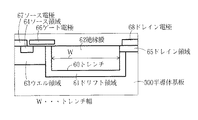
トレンチ技術は、DRAM等のメモリのキャパシタンスを作成する技術、素子分離のSOI技術、またMOSデバイスのトレンチゲートに既に使用されているが、近年パワーICへの適用が検討され、図43に示すような横型高耐圧MOSFETへの応用も提案されている(特許文献1)。
この横型高耐圧MOSFETの構造について説明する。半導体基板300にトレンチ60を形成し、このトレンチ60に沿ってドリフト領域61を形成し、トレンチ60を絶縁膜62で充填し、半導体基板300の表面層にウエル領域63を形成する。ウエル領域63の表面層にドリフト領域61と離してソース領域64を形成し、ソース領域64とドリフト領域61に挟まれたウエル領域63上に図示しないゲート絶縁膜を介してゲート電極66が形成され、半導体基板300の表面層にドリフト領域61と接してドレイン領域65を形成する。ソース領域64上とドレイン領域65上にソース電極67とドレイン電極68をそれぞれ形成する。前記したドリフト領域61は、トレンチ内壁に高濃度にドープされた多結晶シリコン膜を形成し、熱処理して、この多結晶シリコン層を拡散源として、トレンチに沿うように、半導体基板300に拡散層を形成することで形成される。
【0003】
トレンチ幅Wが広く、トレンチ開口率(トレンチの開口部面積のウエハ面積に占める割合)の大きなデバイスを製作する場合、幅広トレンチ内にブラックシリコンと呼ばれる柱状の突起物が形成される(特許文献2)。
このブラックシリコンの発生メカニズムはつぎのように推測される。一回で幅の広いトレンチを形成する場合、そのエッチングする面積が大面積となり、シリコンのエッチングにより発生した反応生成物であるSiOなどが被エッチング面に堆積し、それがマスクとして作用することによってSiOの下のシリコンがエッチングされずにエッチングが進み、結果としてトレンチ内に柱状のシリコンが残りブラックシリコンとなる。
【0004】
【特許文献1】
USP5844275号公報
【特許文献2】
特開2002−64089号公報
【0005】
【発明が解決しようとする課題】
このようにブラックシリコンが発生すると、トレンチ内に充填した絶縁膜の膜質が低下し、もれ電流が増大する。またシリコンの突起部で電界集中を生じて、耐圧不良を引起す。また、後工程においてこの柱状の突起物が折れてパーティクル発生の原因や拡散炉の汚染原因になり、製造良品率を低下させる。
また、前記のように、大面積をエッチングするとウェハの反りが発生する。開口率(ウェハ面積に対するエッチング面積の比率)が大きくなるほどウェハの反りも大きくなり、この結果、フォトリソグラフィ工程時にウェハに形成されるパターンの精度が低下し、トレンチ形状の精度よい制御が困難になる。また、ウェハの反りが大きくなると、半導体製造装置でウェハの移載などが行えなくなるといった不具合が生じる。
【0006】
また、開口部が大きく、開口部の幅と同程度の深さのトレンチの内部を酸化膜などの絶縁膜で埋め込む場合、減圧CVD(Chemical Vapor Deposition)法を用いた場合には、少なくともトレンチの開口部の幅(トレンチ幅)の半分以上の厚い膜を形成しなければならない。例えば、トレンチ幅及びトレンチの深さが20μmの場合には、10μmもの厚い膜を形成しなければならず、非常に時間のかかる膜形成工程となるために製造コストが増大する。
また、図43の半導体装置を製造する場合に、拡散源となる高濃度にドープした多結晶シリコン層を付けたままで、トレンチ内に絶縁膜を充填する工程や、ウエル領域、ソース・ドレイン領域などを形成する工程を実施すると、熱処理により、ドリフト領域の不純物濃度が所定値から変化したり、拡散源の不純物が前記領域に拡散して、所定の特性が得られなくなったり、信頼性の低下を招いたりする。
【0007】
また、トレンチ内を充填する絶縁膜を酸化膜とした場合、この酸化膜を形成するための熱酸化工程で多結晶シリコン層が酸化膜に変質する。しかし、この変質した酸化膜の膜質は必ずしも良質でなく、また、この変質した酸化膜と熱酸化膜との間で歪みが発生し、耐圧特性などの信頼性が低下する。
この発明は、前記の課題を解決して、トレンチ底面に発生するブラックシリコンを抑制し、ウェハの反りを抑制し、トレンチを囲むように形成されるドリフト領域の不純物濃度を所定値に確保し、トレンチ内を充填する絶縁膜の信頼性を確保できる半導体装置の製造方法を提供することにある。
【0008】
【課題を解決するための手段】
前記の目的を達成するために、(1)半導体基板の表面層にアスペクト比が1以上の溝を複数個近接して形成する工程と、該溝で挟まれた半導体領域を除去し、前記半導体装置にトレンチを形成する工程とを有する製造方法とする。
(2)半導体基板の表面層にアスペクト比が1以上の溝を複数個近接して形成する工程と、該溝で挟まれた半導体領域を完全に酸化膜に変質するまで酸化する工程と、該酸化された前記半導体領域を除去し、前記半導体基板にトレンチを形成する工程とを有する製造方法とする。
(3)半導体基板の表面層にアスペクト比が1以上の溝を複数本ループ状に形成する工程と、該溝で挟まれた半導体領域を除去し、半導体基板にトレンチを形成する工程とを有する製造方法とする。
(4)半導体基板の表面層にアスペクト比が1以上の溝を複数本ループ状に形成する工程と、該溝で挟まれた半導体領域を完全に酸化膜に変質するまで酸化する工程と、酸化膜に変質した前記半導体領域を除去し、前記半導体基板にトレンチを形成する工程とを有する製造方法とする。
(5)半導体基板の表面層にアスペクト比が1以上の半導体領域を囲む第1溝と、該第1溝で囲まれる半導体領域に、前記第1溝と開口部の幅と溝深さが同じ第2溝を同時に形成する工程と、前記溝に挟まれた前記半導体領域を除去し、半導体基板にトレンチ溝を形成する工程とを有する製造方法とする。
(6)半導体基板の表面層にアスペクト比が1以上の半導体領域を囲む第1溝と、該第1溝で囲まれる半導体領域に、前記第1溝と開口部の幅と溝深さが同じ第2溝を同時に形成する工程と、前記溝に挟まれた前記半導体領域を完全に酸化膜に変質するまで酸化する工程と、酸化膜に変質した前記半導体領域を除去し、半導体基板にトレンチを形成する工程とを有する製造方法とする。
(7)半導体基板の表面層にアスペクト比が1以上の溝を複数個近接して形成する工程と、該溝で挟まれた半導体領域を酸化膜に変質する工程と、該溝で挟まれ酸化膜に変質しない半導体領域を除去する工程と、酸化膜に変質した前記半導体領域を除去し、前記半導体基板にトレンチを形成する工程とを有する製造方法とする。
【0009】
(8)半導体基板の表面層にアスペクト比が1以上の溝を複数本ループ状に形成する工程と、該溝で挟まれた半導体領域を酸化膜に変質する工程と、該溝で挟まれ酸化膜に変質しない半導体領域を除去する工程と、酸化膜に変質した前記半導体領域を除去し、前記半導体基板にトレンチを形成する工程とを有する製造方法とする。
(9)半導体基板の表面層にアスペクト比が1以上の半導体領域を囲む第1溝と、該第1溝で囲まれる半導体領域に、前記第1溝と開口部の幅と溝深さが同じ第2溝を同時に形成する工程と、前記前記溝に挟まれた前記半導体領域を酸化膜に変質する工程と、該溝で挟まれ酸化膜に変質しない前記半導体領域を除去する工程と、酸化膜に変質した前記半導体領域を除去し、前記半導体基板にトレンチを形成する工程とを有する製造方法とする。
(10)(1)〜(9)の製造方法において、前記トレンチを形成する工程に続いて、該トレンチ内に絶縁膜を充填する工程を有する製造方法とする。
(11)半導体基板の表面層にアスペクト比が1以上の溝を複数本ループ状に形成する工程と、該溝で挟まれた半導体領域を酸化膜に変質する工程と、該溝で挟まれ酸化膜に変質しない半導体領域を除去する工程と、該除去された半導体領域の箇所と前記溝に絶縁膜を充填する工程とを有する製造方法とする。
(12)半導体基板の表面層にアスペクト比が1以上の半導体領域を囲む第1溝と、該第1溝で囲まれる半導体領域に、前記第1溝と開口部の幅と溝深さが同じ第2溝を同時に形成する工程と、前記前記溝に挟まれた前記半導体領域を酸化膜に変質する工程と、該溝で挟まれ酸化膜に変質しない半導体領域を除去する工程と、該除去された半導体領域の箇所と前記溝に絶縁膜を充填する工程とを有する製造方法とする。
(13)(1)から(9)の製造方法において、前記トレンチを形成する工程に続いて、該トレンチ内壁と接するドリフト領域となる拡散層を形成する工程と、該トレンチ内に絶縁膜を充填する工程とを有する製造方法とする。
(14)半導体基板の表面層にアスペクト比が1以上の溝を複数個近接して形成する工程と、該溝の内壁に不純物をドープした多結晶シリコン層を形成する工程と、該多結晶シリコン層と溝で挟まれた半導体領域を完全に酸化膜に変質するまで熱酸化処理し、該熱酸化処理で、前記多結晶シリコン層を拡散源として溝近傍の半導体領域にドリフト領域となる拡散層を形成する工程と、酸化膜に変質した前記多結晶シリコン層を除去する工程と、前記溝を絶縁膜で充填する工程とを有する製造方法とする。
【0010】
(15)半導体基板の表面層にアスペクト比が1以上の溝を複数本ループ状に形成する工程と、該溝の内壁に不純物をドープした多結晶シリコン層を形成する工程と、該多結晶シリコン層と溝で挟まれた半導体領域を完全に酸化膜に変質するまで熱酸化処理し、該熱酸化処理で、前記多結晶シリコン層を拡散源として溝近傍の半導体領域にドリフト領域となる拡散層を形成する工程と、酸化膜に変質した前記多結晶シリコン層を除去する工程と、前記溝を絶縁膜で充填する工程とを有する製造方法とする。
(16)半導体基板の表面層にアスペクト比が1以上の半導体領域を囲む第1溝と、該第1溝で囲まれる半導体領域に、前記第1溝と開口部の幅と溝深さが同じ第2溝を同時に形成する工程と、該第1溝および第2溝の内壁に不純物をドープした多結晶シリコン層を形成する工程と、該多結晶シリコン層と前記溝で挟まれた半導体領域を完全に酸化膜に変質するまで熱酸化処理し、該熱酸化処理で、前記多結晶シリコン層を拡散源として溝近傍の半導体領域にドリフト領域となる拡散層を形成する工程と、酸化膜に変質した前記多結晶シリコン層を除去する工程と、前記溝を絶縁膜で充填する工程とを有する製造方法とする。
(17)半導体基板の表面層にアスペクト比が1以上の溝を複数個近接して形成する工程と、該溝の内壁に不純物をドープした多結晶シリコン層を形成する工程と、該多結晶シリコン層と溝で挟まれた半導体領域を酸化膜に変質するまで熱酸化処理し、該熱酸化処理で、前記多結晶シリコン層を拡散源として溝近傍の半導体領域にドリフト領域となる拡散層を形成する工程と、酸化膜に変質しない前記半導体領域を除去し、該除去箇所に前記拡散層と接するドリフト層の一部となる拡散層を形成する工程と、前記溝と除去された前記半導体領域の箇所を絶縁膜で充填する工程とを有する製造方法とする。
【0011】
(18)半導体基板の表面層にアスペクト比が1以上の溝を複数個近接して形成する工程と、該溝の内壁に不純物をドープした多結晶シリコン層を形成する工程と、該多結晶シリコン層と溝で挟まれた半導体領域を酸化膜に変質するまで熱酸化処理し、該熱酸化処理で、前記多結晶シリコン層を拡散源として溝近傍の半導体領域にドリフト領域となる拡散層を形成する工程と、酸化膜に変質した前記多結晶シリコン層を除去する工程と、酸化膜に変質しない前記半導体領域を除去し、該除去箇所に前記拡散層と接するドリフト層の一部となる拡散層を形成する工程と、前記溝と除去された前記半導体領域の箇所を絶縁膜で充填する工程とを有する製造方法とする。
(19)半導体基板の表面層にアスペクト比が1以上の溝を複数本ループ状に形成する工程と、該溝の内壁に不純物をドープした多結晶シリコン層を形成する工程と、該多結晶シリコン層と溝で挟まれた半導体領域を酸化膜に変質するまで熱酸化処理し、該熱酸化処理で、前記多結晶シリコン層を拡散源として溝近傍の半導体領域にドリフト領域となる拡散層を形成する工程と、酸化膜に変質しない前記半導体領域を除去し、該除去箇所に前記拡散層と接するドリフト層の一部となる拡散層を形成する工程と、前記溝と除去された前記半導体領域の箇所を絶縁膜で充填する工程とを有する製造方法とする。
(20)半導体基板の表面層にアスペクト比が1以上の溝を複数本ループ状に形成する工程と、該溝の内壁に不純物をドープした多結晶シリコン層を形成する工程と、該多結晶シリコン層と溝で挟まれた半導体領域を酸化膜に変質するまで熱酸化処理し、該熱酸化処理で、前記多結晶シリコン層を拡散源として溝近傍の半導体領域にドリフト領域となる拡散層を形成する工程と、酸化膜に変質した前記多結晶シリコン層を除去する工程と、酸化膜に変質しない前記半導体領域を除去し、該除去箇所に前記拡散層と接するドリフト層の一部となる拡散層を形成する工程と、前記溝と除去された前記半導体領域の箇所を絶縁膜で充填する工程とを有する製造方法とする。
【0012】
(21)半導体基板の表面層にアスペクト比が1以上の半導体領域を囲む第1溝と、該第1溝で囲まれる半導体領域に、前記第1溝と開口部の幅と溝深さが同じ第2溝を同時に形成する工程と、該第1溝と第2溝の内壁に不純物をドープした多結晶シリコン層を形成する工程と、該多結晶シリコン層と溝で挟まれた半導体領域を酸化膜に変質するまで熱酸化処理し、該熱酸化処理で、前記多結晶シリコン層を拡散源として溝近傍の半導体領域にドリフト領域となる拡散層を形成する工程と、酸化膜に変質しない前記半導体領域を除去し、該除去箇所に前記拡散層と接するドリフト層の一部となる拡散層を形成する工程と、前記溝と除去された前記半導体領域の箇所を絶縁膜で充填する工程とを有する製造方法とする。
(22)半導体基板の表面層にアスペクト比が1以上の半導体領域を囲む第1溝と、該第1溝で囲まれる半導体領域に、前記第1溝と開口部の幅と溝深さが同じ第2溝を同時に形成する工程と、該第1溝と第2溝の内壁に不純物をドープした多結晶シリコン層を形成する工程と、該多結晶シリコン層と溝で挟まれた半導体領域を酸化膜に変質するまで熱酸化処理し、該熱酸化処理で、前記多結晶シリコン層を拡散源として溝近傍の半導体領域にドリフト領域となる拡散層を形成する工程と、酸化膜に変質した前記多結晶シリコン層を除去する工程と、酸化膜に変質しない前記半導体領域を除去し、該除去箇所に前記拡散層と接するドリフト層の一部となる拡散層を形成する工程と、前記溝と除去された前記半導体領域の箇所を絶縁膜で充填する工程とを有する製造方法とする。
【0013】
(23)(14)〜(22)の半導体装置の製造方法において、前記溝の内壁に多結晶シリコン層を形成する工程を、イオン注入層を形成する工程に置き換えるてもよい。
(24)(14)〜(22)の半導体装置の製造方法において、前記溝の内壁に多結晶シリコン層を形成する工程を、イオン注入層を形成した後、熱処理する工程に置き換えるてもよい。
(25)(5)、(6)、(9)、(13)、(15)、(16)、(21)〜(24)の半導体装置の製造方法において、前記第2溝の両端が前記第1溝と接し、前記第2溝の平面形状がストライプ状をしているとよい。
(26)(5)、(6)、(9)、(13)、(15)、(16)、(21)〜(24)の半導体装置の製造方法において、前記第2溝の平面形状が格子状であり、該格子の外周端が前記第1溝と接するとよい。
(27)(1)〜(24)の半導体装置の製造方法において、前記溝で挟まれた前記半導体領域および酸化膜に変質した前記半導体領域を除去する方法が、等方性エッチング法であるとよい。
(28)半導体基板の表面層にトレンチを形成する工程と、該トレンチの内壁に不純物をドープした多結晶シリコン層を形成する工程と、該多結晶シリコン層を完全に酸化膜に変質するまで熱酸化処理し、該熱酸化処理で、トレンチと接する半導体基板にドリフト領域となる拡散層を形成する工程と、酸化膜に変質した前記多結晶シリコン層を除去する工程と、前記トレンチを絶縁膜で充填する工程とを有する製造方法とする。
(29)(13)〜(28)の半導体装置の製造方法において、前記ドリフト領域を形成する工程に続いて、前記半導体基板上にゲート電極を形成する工程と、該ドリフト領域を挟んで前記半導体基板の表面層にソース領域およびドレイン領域を形成する工程とを有する製造方法とする。
〔作用〕
トレンチを形成する領域にアスペクト比が1以上の微小な溝を近接して多数形成することで、溝底部にブラックシリコンが形成されることを防止できる。
【0014】
また、溝で挟まれるシリコン柱の幅を広くして、熱酸化によりシリコン柱が熱酸化膜に変質した箇所を残し、変質しない箇所のシリコンを除去することで、幅広のトレンチ内に熱酸化膜に変質したシリコン柱を残すことで、その後の工程でウエハが反ることを防止できる。
また、ドレイン領域を形成した後で、拡散源のドープされたポリシリコン層を除去することで、後工程の熱処理で、ドレイン領域の不純物濃度が変わることを防止できる。また、ドレイン領域以外の拡散層に拡散源の不純物が拡散することを防止できる。
【0015】
【発明の実施の形態】
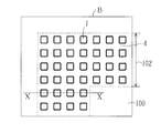
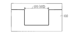
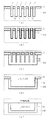
図1から図11は、本発明の半導体装置の製造方法の内、トレンチを形成する方法の概要を説明する図である。図1は、半導体基板にトレンチを形成した平面図であり、図2から図7は微小の溝を形成した平面図であり、図8は図2から図7の断面図であり、図9はトレンチの断面図であり、図10、図11はトレンチの平面図である。
図1は、半導体基板にトレンチを形成した平面図である。トレンチ101はストライプ状のものであり、トレンチ102はリング状をしたものである。図示しないが、トレンチ101、102に絶縁膜が充填されて、誘電体分離領域が形成されたり、このトレンチに沿うように横型高耐圧MOSFETなどのドリフト領域が形成される。
【0016】
図2、図3は、図1のA部およびB部の拡大図である。このトレンチ101、102内には、微小な独立した平面が正方形の溝1が近接して形成されている 。この溝のアスペクト比は1以上である。また溝1で囲まれた(挟まれた)半導体基板100は格子状をしたシリコン柱4となる。
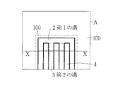
図4は、図1のA部の拡大図である。これは図2とは異なった例である。トレンチ101は微小な第1の溝2で枠取りされており、この枠取りされた内側に、複数本のストライプ状の第2の溝3が第1の溝2にその両端が接するように、しかも互いが近接するように、第1の溝2と同時に形成される。この第1および第2の溝2、3のアスペクト比は1以上である。第1の溝2に囲まれた箇所(挟まれた箇所)がストライプ状のシリコン柱4となる。
【0017】
図5は、図4の変形例であり、図4の複数本のシリコン柱4が途中で切断され、格子状の溝となった場合である。図4ではシリコン柱4の平面形状は長方形となっているが、互いに近接した正方形の場合もある。
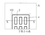
図6は、図1のB部の拡大図である。これは、図3と異なった例である。トレンチ102の外周端と内周端に微小な第1の溝2が形成されており、この第1の溝2で挟まれた領域に、複数本のリング状の第2の溝3が近接して、第1の溝2と同時に形成される。この第1および第2の溝2、3のアスペクト比は1以上である。第1の溝2、第2の溝3および第2の溝3で挟まれた箇所がリング状のシリコン柱4となる。
【0018】
図7は、図6の変形例であり、図6の複数本のシリコン柱4が途中で切断され、格子状の溝となり、コーナー部のシリコン柱4の平面形状は鉤状となっているが、円弧状の場合もある。また、全域で微小な正方形の場合もある。
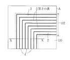
図8は、図2から図7のX−X線で切断した要部断面図である。図中の1は図2、図3の溝であり、(2)で示した溝は、図4から図7の第1の溝2であり、(3)で示した溝は、図4から図7の第2の溝3である。これらの溝に挟まれた箇所がシリコン柱4となる。
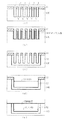
図9は、最終的に形成されるトレンチの断面形状であり、図10、図11はその平面図である。図9は、図10、図11のX−X線で切断した断面図である。図8で示すアスペクト比が1以上の溝で挟まれたシリコン柱4を除去することで、幅広のトレンチが形成できる。
【0019】
多数の微小な溝1、2、3を形成することで、幅広のトレンチを一回のエッチングで形成する場合と比べて、エッチングによる反応生成物(SiOなど)を少なくできて、この反応生成物で発生する微小なブラックシリコンも、その後のシリコン柱4を除去する工程で除去されるために、ブラックシリコンの発生を抑えることができる。
そのため、例えば、20μm幅で20μm深さの幅広で深いトレンチを形成する場合、2μm幅で20μm深さの微小な溝を多数形成し、その後、シリコン柱を除去して20μm幅で20μm深さのトレンチを形成することで、ブラックシリコンの発生を抑制できる。つまり、微小な溝の幅は深さより小さくするほどブラックシリコンの発生は抑制できることになる。そのため、本発明では、微小な溝のアスペクト比を1以上とした。アスペクト比とは溝の深さを幅で割った値であり、アスペクト比が1以上ということは、溝の深さが溝の幅以上に深いということを意味する。
【0020】
つぎに、具体的な実施例について説明する。ここでは、図2、図3の場合を例として挙げたが、図4から図7の場合も同様である。
図12は、この発明の第1実施例の半導体装置の製造方法であり、同図(a)から同図(c)は工程順に示した要部製造工程断面図である。
半導体基板100を、絶縁膜11をマスクとして、アスペクト1以上の溝1を近接して形成する。この溝1に挟まれた箇所がシリコン柱4となる。溝1およびシリコン注4の幅は1μm程度である。溝1の形成は、絶縁膜11をマスクとしてRIE(Reactive Ion Etching)法などの異方性ドライエッチングを行う。また、絶縁膜11は、酸化膜や窒化膜である(同図(a))。
【0021】
つぎに、図示しないレジストをマスクとして、シリコン柱4上の絶縁膜11を除去する。絶縁膜11が酸化膜の場合はフッ酸溶液などで容易に除去できる(同図(b))。
つぎに、CDE(Chemical Dry Etching)法等の等方性ドライエッチングによりシリコン柱4を除去すことで、トレンチ101、102が形成される(同図(c))。
前記の溝1幅を狭くすることで、ブラックシリコンの発生は抑制される。
図13は、この発明の第2実施例の半導体装置の製造方法であり、同図(a)から同図(d)は工程順に示した要部製造工程断面図である。
【0022】
図12との違いは、シリコン柱4を熱酸化により、シリコン柱4全体を熱酸化膜12に変質させ(同図(b))、その後、フッ酸溶液などでこの熱酸化膜12を除去することで、トレンチを形成する(同図(c))点である。図12と比べると、熱酸化膜12に変質したシリコン柱を容易に除去できる。
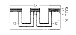
つぎに、このトレンチ101、102に絶縁膜を充填して誘電体分離領域などを形成する場合について説明する。
図14は、この発明の第3実施例の半導体装置の製造工程断面図である。この工程断面図は、前記したトレンチ101、102に絶縁膜を充填した図である。
【0023】
これは、図11、図12の工程に続いて、絶縁膜13をトレンチ101、102の深さより、高くなるように全面に形成した後、CMP(Chemical Mechanical Plishing)法で半導体基板100より高い余分な絶縁膜13および絶縁膜11を除去して平坦化し、トレンチ101、102内の絶縁膜13の表面高さを半導体基板100の表面高さと同じ高さになるようする。
このように、トレンチ101、102に絶縁膜13を充填することで、図1のBのようなリング状のトレンチの場合には、誘電体分離領域とすることができる。
【0024】
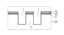
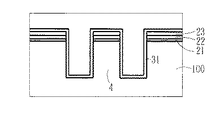
図15から図20は、この発明の第3実施例の半導体装置の製造方法であり、工程順に示した要部製造工程断面図である。
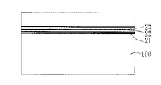
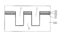
半導体基板100上に30nm厚さの酸化膜21(熱酸化膜)、100nm厚さの窒化膜22(CVD(Chemical Vapor Deposition)法で形成)、1μm厚さの酸化膜23(減圧CVD法で形成)を形成する。これら3層の絶縁膜は微小な溝を形成する場合のマスクとして用いられる。また、熱酸化するときのマスクの働きもする(図15)。
つぎに、半導体基板100に、微小な溝1の互いの間隔を2μmにして形成する。溝1の幅は2μm、深さは20μmでアスペクト比が10である。このアスペクト比が50を超すと後工程での洗浄でシリコン柱4が根元から折れて、エッチング不良やパーティクルの原因となる。また、シリコン柱4の幅は2μm程度とする(図16)。
【0025】
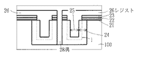
つぎに、溝1の周囲に熱酸化膜24を形成する。シリコン柱4の幅が2μm程度と広いために、この熱酸化ではシリコン柱4を完全には熱酸化膜24に変質させることができず、未酸化領域27が発生する。また、この熱酸化膜24で囲まれ、溝1より浅い溝25が形成される(図17)。
つぎに、未酸化領域27上を開口したレジスト26を形成し、このレジスト26をマスクに未酸化領域27をRIE法で異方性ドライエッチングして除去する(図18)。
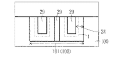
つぎに、レジスト26を除去し、絶縁膜29を溝25、28を覆うように全面に形成する(図19)。
【0026】
つぎに、CMP法で絶縁膜29、酸化膜21、窒化膜22、酸化膜23を、半導体基板100の表面高さまで除去する(図20)。
このように、シリコン柱4の幅を広くして、未酸化領域27を除去することで、幅20μm程度のトレンチ101、102を形成することができる。
また、広いトレンチ幅でも、熱酸化膜24に変質したシリコン柱を残すことで、ウエハ裏面の図示しない酸化膜とのバランスがとれるため、ウエハの反りを抑制できる。さらに、熱酸化膜24に変質したシリコンはしら残すと、前記第1、第2実施例と比べ絶縁膜29の溝内への形成時間を短縮することができる。また、複数解に分け、1回のエッチング開口率を低くして、トレンチを掘ることによっても、プロセス途中でのウエハの反りを抑制できる。また、溝1を微小とすることで、ブラックシリコンの発生を防止できる。
【0027】
【表1】

【0028】
本発明の場合は、トレンチ101、102内に熱酸化膜24に変質したシリコン柱が存在するため、ウエハの反りが小さく、開口率が70%でも搬送エラーが起きなかった。一方、従来の場合は開口率40%で搬送エラーが起こった。
【0029】
【表2】
溝の幅が10μmまではブラックシリコンは発生しないが、12μm以上ではブラックシリコンは発生するようになる。表2に示さないが、開口率70%とすると、溝幅が4μmまではブラックシリコンが発生しない。
【0030】
このブラックシリコンの発生は、前記したように、シリコンのエッチングにより発生した反応生成物が被エッチング面に付着して起こるため、溝幅(溝の開口部の大きさ)が大きくなると発生し易くなり、また、溝の総数(開口率)が大きくなると発生し易くなる。よって、1回のエッチングの開口率を35%以下として、トレンチ幅10μm以下とすればよい。
図21、図22は、図18の段階での平面図である。図21は、図3に相当する平面図で、図22は、図6に相当する平面図である。これらの平面図から溝28の平面形状が分かる。
【0031】
つぎに、横型高耐圧MOSFETなどのドリフト領域を形成して、トレンチを絶縁膜で充填する場合の製造方法について説明する。以下の説明ではドリフト領域となる拡散層32の導電形を示さないが、nチャネルMOSFETを形成する場合はn形であり、pチャネルMOSFETを形成する場合はp形である。
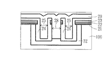
図23は、この発明の第4実施例の半導体装置の製造方法であり、同図(a)から同図(d)は、工程順に示した要部製造工程断面図である。
図12、図13の工程に続いて、全面にドープしたポリシリコン層31を形成する(同図(a))。
【0032】
つぎに、熱処理して、ドリフト領域となる拡散層32を形成する(同図(b))。
つぎに、ポリシリコン層31を除去する(同図(c))。
つぎに、トレンチ101、102が埋まるように全面に絶縁膜33を形成し、半導体基板100の表面が露出するまで、CMP法で絶縁膜33と絶縁膜11を研削除去し、平坦化する(同図(d))。
拡散源となるポリシリコン層31を除去することで、後工程での熱処理で、ドリフト領域の不純物濃度が変化することを防止して、所定の不純物濃度を得ることができる。
【0033】
図24は、この発明の第5実施例の半導体装置の製造方法であり、同図(a)から同図(e)は、工程順に示した要部製造工程断面図である。
半導体基板100を、絶縁膜11をマスクとして、アスペクト比1以上(例えばアスペクト比10程度)の溝1を近接して形成する。
つぎに、全面に、ドープしたポリシリコン層31(例えば、厚さが30nm程度)を減圧CVD法で形成する(同図(b)。
つぎに、ポリシリコン層31を拡散源として、シリコン柱4の底部で拡散層が繋がるまで、例えば、1150℃、120分の熱処理を行い、ドリフト領域となる拡散層32を、例えば、ピーク濃度1×1016cm−3で幅3μmとなるように形成する(同図(c))。
【0034】
つぎに、ポリシリコン層31とシリコン柱4を除去して、トレンチ101、102を形成する。この場合、ポリシリコン層31とシリコン柱4を熱酸化膜に変質した後、これらを除去しても構わない(同図(d))。
つぎに、トレンチ101、102が埋まるように全面に絶縁膜33を形成し、半導体基板100の表面が露出するまで、CMP法で絶縁膜33と絶縁膜11を研削除去し、平坦化する(同図(e))。
図25は、この発明の第6実施例の半導体装置の製造方法であり、同図(a)から同図(e)は、工程順に示した要部製造工程断面図である。
【0035】
半導体基板100を、絶縁膜11をマスクとして、アスペクト比1以上(例えば、アスペクト比10程度)の溝1を近接して形成する。
つぎに、全面にイオン注入層34を形成する(同図(b))。
つぎに、イオン注入層34を拡散源として、シリコン柱4の底部で拡散層が繋がるまで熱処理し、ドリフト領域となる拡散層32(ピーク濃度1×1016cm−3で幅3μm)を形成する(同図(c))。
つぎに、シリコン柱4を除去して、トレンチ101、102を形成する。この場合、シリコン柱4を熱酸化膜に変質した後、これらを除去しても構わない(同図(d))。
【0036】
つぎに、トレンチ101、102が埋まるように全面に絶縁膜33を形成し、半導体基板100の表面が露出するまで、CMP法で絶縁膜33と絶縁膜11を研削除去し、平坦化する(同図(e))。
つぎに、シリコン柱の幅が広く、シリコン柱全域が熱酸化膜に変質できない場合について説明する。
図26から図32は、この発明の第7実施例の半導体装置の製造方法であり、工程順に示した要部製造工程断面図である。
半導体基板100上に30nm厚さの酸化膜21(熱酸化膜)、100nm厚さの窒化膜22(CVD(Chemical Vapor Deposition)法で形成)、1μm厚さの酸化膜23(減圧CVD法で形成)を形成する。これら3層の絶縁膜は微小な溝を形成する場合のマスクとして用いられる。また、熱酸化するときのマスクの働きもする(図26)。
【0037】
つぎに、半導体基板100に、微小な溝1の互いの間隔を2μmにして形成する。溝1の幅は2μm、深さは20μmでアスペクト比が10である。この溝1はRIE法による異方性ドライエッチングで形成される(図27)。
つぎに、全面に、ドープしたポリシリコン層31(例えば、厚さが30nm程度)を減圧CVD法で形成する(図28)。
つぎに、ポリシリコン層31を拡散源として、シリコン柱4の底部で拡散層が繋がるまで、例えば、1150℃、120分の熱処理を行い、ドリフト領域となる拡散層32を、例えば、ピーク濃度1×1016cm−3で幅3μmとなるように形成する。その後、熱酸化して、ポリシリコン層31と拡散層32の表面層を熱酸化膜24に変質させる。シリコン柱4の幅が広いために、この熱酸化ではシリコン柱4を完全には熱酸化膜24に変質させることができず、未酸化領域27が発生する。また、この熱酸化膜24で囲まれ、溝1より浅い溝25が形成される(図29)。
【0038】
つぎに、未酸化領域27上を開口したレジスト26を形成し、未酸化領域を除去する(図30)。
つぎに、レジスト26を除去し、絶縁膜29を溝25、28を覆うように全面に形成する(図31)。
つぎに、CMP法で絶縁膜29、酸化膜21、窒化膜22、酸化膜23を、半導体基板100の表面高さまで除去し平坦化する。このとき、窒化膜22をストッパとしてCMP法で第1次の平坦化を図り、その後、窒化膜22と酸化膜23および絶縁膜29をエッチングによって最終的に平坦化しても構わない(図32)。
【0039】
前記したように、シリコン柱4の幅を広くし、未拡散領域27を除去することで、トレンチの幅を広くすることができる。
また、広いトレンチ幅でも、熱酸化膜24に変質したシリコン柱を残すことで、ウエハの反りを防止でき、また、溝1を微小とすることで、ブラックシリコンの発生を防止できる。
図33は、この発明の第8実施例の半導体装置の製造方法であり、同図(a)から同図(d)は工程順に示した要部製造工程断面図である。
図28の工程に続いて、ポリシリコン層31を拡散源として、シリコン柱4の底部で拡散層が繋がるまで熱処理し、ドリフト領域となる拡散層32を形成する。その後、この拡散源となるポリシリコン層31を除去し、その後で熱酸化して、拡散層32の表面層を熱酸化膜24に変質させる。ポリシリコン層31の除去は熱酸化膜に変質させた後に希フッ酸溶液などで行っても構わない。シリコン柱4の幅が広いために、この熱酸化ではシリコン柱4を完全には熱酸化膜24に変質させることができず、未酸化領域27が発生する。また、この熱酸化膜24で囲まれ、溝1より浅い溝25が形成される(同図(a))。
【0040】
つぎに、未酸化領域27上を開口したレジスト26を形成し、未酸化領域を除去する(同図(b))。
つぎに、レジスト26を除去し、絶縁膜29を溝25、28を覆うように全面に形成する(同図(c))。
つぎに、CMP法で絶縁膜29、酸化膜21、窒化膜22、酸化膜23を、半導体基板100の表面高さまで除去し平坦化する(同図(d))。
このように、拡散源となるポリシリコン層31を除去することで、後工程での熱処理で、ドリフト領域の不純物濃度が変化することを防止して、所定の不純物濃度を得ることができる。
【0041】
また、前記したように、未拡散領域27を除去することで、シリコン柱4の幅を広くすることができて、トレンチの幅を広くすることができる。
また、広いトレンチ幅でも、熱酸化膜24に変質したシリコン柱を残すことで、ウエハの反りを防止でき、また、溝1を微小とすることで、ブラックシリコンの発生を防止できる。
図34は、この発明の第9実施例の半導体装置の製造方法であり、同図(a)から同図(d)は工程順に示した要部製造工程断面図である。
図28の工程に続いて、ポリシリコン層31を拡散源として、熱処理して、ドリフト領域となる拡散層32を形成する。この熱処理では、シリコン柱4の底部で直接的に拡散層が繋がらず未拡散領域35が残る。その後、熱酸化して、ポリシリコン層31と拡散層32の表面層を熱酸化膜24に変質させる。この熱酸化では拡散層32の表面層が熱酸化膜に変質するために、未酸化領域27が発生する。また、この熱酸化膜24で囲まれ、溝1より浅い溝25が形成される(同図(a))。
【0042】
つぎに、未酸化領域27上を開口したレジスト26を形成し、溝25で挟まれた未酸化領域27を除去し、溝28を形成する。その後で、この溝28の底の半導体基板100にドリフト領域となる拡散層36を拡散層32と接するように形成する(同図(b))。
つぎに、レジスト26を除去し、絶縁膜29を溝25、28を覆うように全面に形成する(同図(c))。
つぎに、CMP法で絶縁膜29、酸化膜21、窒化膜22、酸化膜23を、半導体基板100の表面高さまで除去し、平坦化する(同図(d))。
【0043】
第7実施例と同様の効果が得られるが、第7実施例よりさらに、シリコン柱4の幅を広げて、トレンチの幅を広げることができる。
図35は、この発明の第10実施例の半導体装置の製造方法であり、同図(a)から同図(d)は工程順に示した要部製造工程断面図である。
図28の工程に続いて、ポリシリコン層31を拡散源として、熱処理して、ドリフト領域となる拡散層32を形成する。この熱処理では、シリコン柱4の底部で直接的に拡散層が繋がらず未拡散領域35が残る。その後、この拡散源となるポリシリコン層31を除去し、その後で熱酸化して、拡散層32の表面層を熱酸化膜24に変質させる。シリコン柱4の幅が広いために、この熱酸化ではシリコン柱4を完全には熱酸化膜24に変質させることができず、未酸化領域27が発生する。また、この熱酸化膜24で囲まれ、溝1より浅い溝25が形成される(同図(a))。
【0044】
つぎに、未酸化領域27上を開口したレジスト26を形成し、溝25で挟まれた未酸化領域27を除去し、溝28を形成する。その後で、この溝28の底の半導体基板100にドリフト領域となる拡散層36を拡散層32と接するように形成する(同図(b))。
つぎに、レジスト26を除去し、絶縁膜29を溝25、28を覆うように全面に形成する(同図(c))。
つぎに、CMP法で絶縁膜29、酸化膜21、窒化膜22、酸化膜23を、半導体基板100の表面高さまで除去し、平坦化する(同図(d))。
【0045】
第8実施例と同様の効果が得られるが、第8実施例よりさらに、シリコン柱4の幅が広い場合に有効となる。
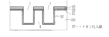
図36から図42は、この発明の第11実施例の半導体装置の製造方法であり、工程順に示した要部製造工程断面図である。
図27の工程に続いて、溝1の内壁に接する半導体基板100にイオン注入層37を形成する(図36)。
つぎに、熱処理し、ドリフト領域となる拡散層32を形成する。この熱処理では、シリコン柱4の底部で直接的に拡散層が繋がらず未拡散領域35が残る(図37)。
【0046】
つぎに、熱酸化して、拡散層32の表面層を熱酸化膜24に変質させる。この熱酸化では拡散層32を完全には熱酸化膜24に変質させることができず、未酸化領域27が発生する。また、この熱酸化膜24で囲まれ、図示しない溝1より浅い溝25が形成される(図38))。
つぎに、未酸化領域27上を開口したレジスト26を形成し、溝25で挟まれた未酸化領域27を除去し、溝28を形成する。その後で、この溝28の底の半導体基板100にドリフト領域となる拡散層36を拡散層32と接するように形成する(図39)。
【0047】
つぎに、レジスト26を除去し、絶縁膜29を溝25、28を覆うように全面に形成する(図40)。
つぎに、CMP法で絶縁膜29、酸化膜21、窒化膜22、酸化膜23を、半導体基板100の表面高さまで除去し、平坦化する(図41)。
前記した実施例と同様の効果が得られる。
つぎに、前記した実施例を用いて横型高耐圧MOSFETの製造方法について説明する。
図42は、この発明の第12実施例の半導体装置の要部製造工程断面図である。
【0048】
図23(d)、図24(e)、図25(e)、図32、図33(d)、図34(d)、図35(d)および図41の工程に続いて、ドリフト領域51に接するウエル領域53を半導体基板100の表面層に形成し、このウエル領域53の表面層にソース領域54を形成する。また、ドリフト領域51と接するドレイン領域を半導体基板100の表面層に形成する。ソース領域54とドリフト領域51に挟まれた半導体基板100上に図示しないゲート絶縁膜を介してゲート電極56を形成する。ソース領域54上とドレイン領域55上にソース電極57とドレイン電極58をそれぞれ形成して、トレンチに沿うドリフト領域51を有する横型高耐圧MOSFETが製作される。
【0049】
尚、ドリフト領域51は、前記した各図の拡散層32、36である。また、絶縁膜52は、前記した各図の24、29、33である。
このようにして製作された高耐圧横型MOSFETは、その耐圧は数100Vであり、また、微小な溝を形成した後でトレンチを形成するため、ブラックシリコンの発生が抑制され、トレンチ部での耐圧特性を向上できる。また、トレンチに沿うドレイン領域のため、ソース・ドレインの平面距離を短くできて、単位面積当りのオン抵抗を低減できる。
また、ドレイン領域を形成した後、拡散源を除去することで、後工程でのドリフト領域の不純物濃度の変調や他領域への汚染(拡散源からの拡散)を防止できる。また、トレンチ内に熱酸化したシリコン柱を残留させることで、幅広のトレンチ幅でもウエハの反りを抑制できて、半導体製造装置での搬送エラーの発生を防止できる。
【0050】
【発明の効果】
この発明によれば、微小な溝を多数形成し、その後、この微小な溝で挟まれた多数の微小な半導体柱(シリコン柱)を除去してトレンチを形成することで、トレンチ底面に発生するブラックシリコンを抑制することができる。
このブラックシリコンの発生を抑制することで、素子の電気的特性の向上と信頼性の向上を図ることができる。
また、微小な半導体柱が熱酸化膜に変質した箇所をトレンチ内で残留させることで、ウエハ裏面の酸化膜とのバランスがとれて、ウエハの反りを抑制することができる。また、徐々にトレンチを掘ることで、プロセス途中でのウエハの反りを防止できる。
【0051】
また、微小な溝内に、ドープされたポリシリコン層を形成し、熱処理でドリフト領域となる拡散層を形成した後、ポリシリコン層を除去することで、後工程での熱処理で、ドリフト領域の不純物濃度の変調や他領域への不純物拡散を防止できる。
【図面の簡単な説明】
【図1】半導体基板にトレンチを形成した平面図
【図2】図1のA部の拡大図
【図3】図1のB部の拡大図
【図4】図1のA部の別の拡大図
【図5】図4の変形例の図
【図6】図1のB部の別の拡大図
【図7】図6の変形例の図
【図8】図2から図7のX−X線で切断した要部断面図
【図9】最終的に形成されるトレンチの断面形状であり、図10、図11のX−X線で切断した断面図
【図10】図9の平面図
【図11】図9の別の平面図
【図12】この発明の第1実施例の半導体装置の製造方法であり、(a)から(c)は工程順に示した要部製造工程断面図
【図13】この発明の第2実施例の半導体装置の製造方法であり、(a)から(d)は工程順に示した要部製造工程断面図
【図14】この発明の第3実施例の半導体装置の製造工程断面図
【図15】この発明の第3実施例の半導体装置の要部製造工程断面図
【図16】図15に続く、この発明の第3実施例の半導体装置の要部製造工程断面図
【図17】図16に続く、この発明の第3実施例の半導体装置の要部製造工程断面図
【図18】図17に続く、この発明の第3実施例の半導体装置の要部製造工程断面図
【図19】図18に続く、この発明の第3実施例の半導体装置の要部製造工程断面図
【図20】図19に続く、この発明の第3実施例の半導体装置の要部製造工程断面図
【図21】図18の平面図
【図22】図18の別の平面図
【図23】この発明の第4実施例の半導体装置の製造方法であり、(a)から(d)は、工程順に示した要部製造工程断面図
【図24】この発明の第5実施例の半導体装置の製造方法であり、(a)から(e)は、工程順に示した要部製造工程断面図
【図25】この発明の第6実施例の半導体装置の製造方法であり、(a)から(e)は、工程順に示した要部製造工程断面図
【図26】この発明の第7実施例の半導体装置の要部製造工程断面図
【図27】図26に続く、この発明の第7実施例の半導体装置の要部製造工程断面図
【図28】図27に続く、この発明の第7実施例の半導体装置の要部製造工程断面図
【図29】図28に続く、この発明の第7実施例の半導体装置の要部製造工程断面図
【図30】図29に続く、この発明の第7実施例の半導体装置の要部製造工程断面図
【図31】図30に続く、この発明の第7実施例の半導体装置の要部製造工程断面図
【図32】図31に続く、この発明の第7実施例の半導体装置の要部製造工程断面図
【図33】この発明の第8実施例の半導体装置の製造方法であり、(a)から(d)は工程順に示した要部製造工程断面図
【図34】この発明の第8実施例の半導体装置の製造方法であり、(a)から(d)は工程順に示した要部製造工程断面図
【図35】この発明の第10実施例の半導体装置の製造方法であり、(a)から(d)は工程順に示した要部製造工程断面図
【図36】この発明の第11実施例の半導体装置の要部製造工程断面図
【図37】図36に続く、この発明の第11実施例の半導体装置の要部製造工程断面図
【図38】図37に続く、この発明の第11実施例の半導体装置の要部製造工程断面図
【図39】図38に続く、この発明の第11実施例の半導体装置の要部製造工程断面図
【図40】図39に続く、この発明の第11実施例の半導体装置の要部製造工程断面図
【図41】図40に続く、この発明の第11実施例の半導体装置の要部製造工程断面図
【図42】図41に続く、この発明の第11実施例の半導体装置の要部製造工程断面図
【図43】従来の横型高耐圧MOSFETの要部断面図
【符号の説明】
1、28 溝
2 第1の溝
3 第2の溝
4 シリコン柱
11、13、29、33、52 絶縁膜
12、24 熱酸化膜
21 酸化膜
22 窒化膜
23 酸化膜
25 溝
26 レジスト
27 未酸化領域
31 ポリシリコン層
32 拡散層(ドリフト領域)
34、37 イオン注入層
35 未拡散領域
36 拡散層
51 ドリフト領域
53 ウエル領域
54 ソース領域
55 ドレイン領域
56 ゲート電極
57 ソース電極
58 ドレイン電極
100 半導体基板
101、102 トレンチ
200 半導体チップ[0001]
TECHNICAL FIELD OF THE INVENTION
The present invention relates to a method of manufacturing a semiconductor device having a trench, such as a high-breakdown-voltage MOSFET, and more particularly to a method of manufacturing a trench, an insulating film filling the trench, and a drift region surrounding the trench.
[0002]
[Prior art]
The trench technology has already been used for a technology for creating capacitance of a memory such as a DRAM, an SOI technology for element isolation, and a trench gate for a MOS device. In recent years, application to a power IC has been studied, and as shown in FIG. Application to a simple horizontal high voltage MOSFET has also been proposed (Patent Document 1).
The structure of this lateral high voltage MOSFET will be described. A trench 60 is formed in the
[0003]
When manufacturing a device having a large trench width W and a large trench opening ratio (the ratio of the opening area of the trench to the wafer area), a columnar projection called black silicon is formed in the wide trench (Patent Document 2). ).
The generation mechanism of this black silicon is presumed as follows. When a wide trench is formed at one time, the area to be etched becomes large, and SiO, which is a reaction product generated by etching silicon, is deposited on the surface to be etched, and this acts as a mask. The etching proceeds without etching the silicon under the SiO, and as a result, columnar silicon remains in the trench to become black silicon.
[0004]
[Patent Document 1]
US Pat. No. 5,844,275
[Patent Document 2]
JP-A-2002-64089
[0005]
[Problems to be solved by the invention]
When black silicon is generated in this manner, the quality of the insulating film filled in the trench deteriorates, and the leakage current increases. In addition, electric field concentration occurs at the silicon protrusion, causing a breakdown voltage failure. Further, in a later step, the columnar projections are broken, which causes the generation of particles and the contamination of the diffusion furnace, thereby lowering the yield rate of manufactured non-defective products.
Further, as described above, when a large area is etched, the wafer is warped. As the aperture ratio (the ratio of the etching area to the wafer area) increases, the warpage of the wafer also increases. As a result, the accuracy of the pattern formed on the wafer during the photolithography process decreases, and it becomes difficult to control the trench shape with high accuracy. . In addition, if the warpage of the wafer becomes large, a problem occurs that the wafer cannot be transferred in the semiconductor manufacturing apparatus.
[0006]
When the inside of a trench having a large opening and a depth substantially equal to the width of the opening is buried with an insulating film such as an oxide film, when a low-pressure CVD (Chemical Vapor Deposition) method is used, at least the trench is formed. It is necessary to form a thick film that is at least half the width of the opening (trench width). For example, when the trench width and the trench depth are 20 μm, a film as thick as 10 μm has to be formed, which is a very time-consuming film forming step, and increases the manufacturing cost.
In the case of manufacturing the semiconductor device shown in FIG. 43, a step of filling the trench with an insulating film while keeping the highly doped polycrystalline silicon layer serving as a diffusion source, a well region, a source / drain region, etc. Is performed, the impurity concentration of the drift region changes from a predetermined value due to the heat treatment, the impurity of the diffusion source diffuses into the region, and the predetermined characteristics cannot be obtained or the reliability is reduced. Invite you.
[0007]
If the insulating film filling the trench is an oxide film, the polycrystalline silicon layer is transformed into an oxide film in a thermal oxidation process for forming the oxide film. However, the quality of the deteriorated oxide film is not always good, and distortion occurs between the deteriorated oxide film and the thermal oxide film, thereby lowering reliability such as withstand voltage characteristics.
The present invention solves the above problems, suppresses black silicon generated on the bottom surface of a trench, suppresses warpage of a wafer, and secures a predetermined concentration of an impurity concentration in a drift region formed so as to surround the trench, It is an object of the present invention to provide a method of manufacturing a semiconductor device which can ensure the reliability of an insulating film filling a trench.
[0008]
[Means for Solving the Problems]
In order to achieve the above object, (1) a step of forming a plurality of grooves having an aspect ratio of 1 or more close to each other in a surface layer of a semiconductor substrate, and removing a semiconductor region sandwiched by the grooves; Forming a trench in the device.
(2) a step of forming a plurality of grooves having an aspect ratio of 1 or more close to each other in a surface layer of a semiconductor substrate, and a step of oxidizing a semiconductor region sandwiched by the grooves until the semiconductor region is completely transformed into an oxide film; Removing the oxidized semiconductor region and forming a trench in the semiconductor substrate.
(3) A step of forming a plurality of grooves having an aspect ratio of 1 or more in a loop on the surface layer of the semiconductor substrate, and a step of forming a trench in the semiconductor substrate by removing a semiconductor region sandwiched between the grooves. Manufacturing method.
(4) a step of forming a plurality of grooves having an aspect ratio of 1 or more in a loop on the surface layer of the semiconductor substrate, a step of oxidizing a semiconductor region sandwiched by the grooves until the semiconductor region is completely transformed into an oxide film, Removing the semiconductor region altered to a film and forming a trench in the semiconductor substrate.
(5) The first groove surrounding the semiconductor region having an aspect ratio of 1 or more in the surface layer of the semiconductor substrate, and the semiconductor region surrounded by the first groove has the same width and groove depth as the first groove and the opening. A manufacturing method includes a step of simultaneously forming a second groove and a step of forming a trench in a semiconductor substrate by removing the semiconductor region sandwiched between the grooves.
(6) The first groove surrounding the semiconductor region having an aspect ratio of 1 or more in the surface layer of the semiconductor substrate, and the semiconductor region surrounded by the first groove has the same width and groove depth as the first groove and the opening. Simultaneously forming a second trench, oxidizing the semiconductor region sandwiched between the trenches until the semiconductor region is completely transformed into an oxide film, removing the semiconductor region transformed into an oxide film, and forming a trench in the semiconductor substrate. And a forming step.
(7) a step of forming a plurality of grooves having an aspect ratio of 1 or more close to each other in a surface layer of a semiconductor substrate; a step of transforming a semiconductor region sandwiched between the grooves into an oxide film; A manufacturing method includes a step of removing a semiconductor region that does not change into a film, and a step of removing the semiconductor region that has changed into an oxide film and forming a trench in the semiconductor substrate.
[0009]
(8) a step of forming a plurality of grooves having an aspect ratio of 1 or more in a loop on the surface layer of the semiconductor substrate, a step of transforming a semiconductor region sandwiched by the grooves into an oxide film, and an step of oxidizing the semiconductor region sandwiched by the grooves. A manufacturing method includes a step of removing a semiconductor region that does not change into a film, and a step of removing the semiconductor region that has changed into an oxide film and forming a trench in the semiconductor substrate.
(9) A first groove surrounding the semiconductor region having an aspect ratio of 1 or more in the surface layer of the semiconductor substrate, and the semiconductor region surrounded by the first groove has the same width and groove depth as the first groove and the opening. Simultaneously forming a second trench, transforming the semiconductor region sandwiched between the trenches into an oxide film, removing the semiconductor region sandwiched between the trenches and not transforming into an oxide film, Forming a trench in the semiconductor substrate by removing the altered semiconductor region.
(10) The manufacturing method according to any one of (1) to (9), further comprising, after the step of forming the trench, a step of filling the trench with an insulating film.
(11) a step of forming a plurality of grooves having an aspect ratio of 1 or more in a loop on the surface layer of the semiconductor substrate; a step of transforming a semiconductor region sandwiched by the grooves into an oxide film; A manufacturing method includes a step of removing a semiconductor region which does not change into a film, and a step of filling an insulating film in a location of the removed semiconductor region and the trench.
(12) The first groove surrounding the semiconductor region having an aspect ratio of 1 or more in the surface layer of the semiconductor substrate, and the semiconductor region surrounded by the first groove has the same width and groove depth as the first groove and the opening. Simultaneously forming a second trench, transforming the semiconductor region sandwiched between the trenches into an oxide film, removing a semiconductor region sandwiched between the trenches and not transforming into an oxide film, And a step of filling the trench with an insulating film.
(13) In the manufacturing method according to any one of (1) to (9), following the step of forming the trench, a step of forming a diffusion layer serving as a drift region in contact with the inner wall of the trench, and filling the trench with an insulating film. And a manufacturing method.
(14) a step of forming a plurality of grooves having an aspect ratio of 1 or more close to each other in a surface layer of a semiconductor substrate; a step of forming a polycrystalline silicon layer doped with impurities on the inner wall of the grooves; The semiconductor region sandwiched between the layer and the trench is subjected to thermal oxidation treatment until it completely transforms into an oxide film. In the thermal oxidation treatment, the diffusion layer becomes a drift region in the semiconductor region near the trench using the polycrystalline silicon layer as a diffusion source. , A step of removing the polycrystalline silicon layer transformed into an oxide film, and a step of filling the trench with an insulating film.
[0010]
(15) a step of forming a plurality of grooves having an aspect ratio of 1 or more in a loop on the surface layer of the semiconductor substrate, a step of forming a polycrystalline silicon layer doped with impurities on inner walls of the grooves, The semiconductor region sandwiched between the layer and the trench is subjected to thermal oxidation treatment until it completely transforms into an oxide film. In the thermal oxidation treatment, the diffusion layer becomes a drift region in the semiconductor region near the trench using the polycrystalline silicon layer as a diffusion source. , A step of removing the polycrystalline silicon layer transformed into an oxide film, and a step of filling the trench with an insulating film.
(16) A first groove surrounding the semiconductor region having an aspect ratio of 1 or more in the surface layer of the semiconductor substrate, and the semiconductor region surrounded by the first groove has the same width and groove depth as the first groove and the opening. Forming a second groove simultaneously, forming an impurity-doped polycrystalline silicon layer on inner walls of the first groove and the second groove, and forming a semiconductor region sandwiched between the polycrystalline silicon layer and the groove. A step of forming a diffusion layer that becomes a drift region in a semiconductor region near the trench by using the polycrystalline silicon layer as a diffusion source; and And removing the polycrystalline silicon layer and filling the groove with an insulating film.
(17) a step of forming a plurality of grooves having an aspect ratio of 1 or more close to each other in a surface layer of a semiconductor substrate, a step of forming a polycrystalline silicon layer doped with impurities on inner walls of the grooves, A semiconductor region sandwiched between the layer and the groove is subjected to a thermal oxidation treatment until the semiconductor region is transformed into an oxide film. In the thermal oxidation treatment, a diffusion layer serving as a drift region is formed in the semiconductor region near the groove using the polycrystalline silicon layer as a diffusion source. Removing the semiconductor region that does not change into an oxide film, forming a diffusion layer that becomes a part of the drift layer in contact with the diffusion layer at the removed location, and removing the trench and the removed semiconductor region. Filling a portion with an insulating film.
[0011]
(18) a step of forming a plurality of grooves having an aspect ratio of 1 or more close to each other in a surface layer of a semiconductor substrate, a step of forming a polycrystalline silicon layer doped with impurities on inner walls of the grooves, A semiconductor region sandwiched between the layer and the groove is subjected to a thermal oxidation treatment until the semiconductor region is transformed into an oxide film. In the thermal oxidation treatment, a diffusion layer serving as a drift region is formed in the semiconductor region near the groove using the polycrystalline silicon layer as a diffusion source. Performing a step of removing the polycrystalline silicon layer that has been transformed into an oxide film; removing the semiconductor region that has not been transformed into an oxide film; and forming a diffusion layer that becomes a part of the drift layer in contact with the diffusion layer at the removed portion. And a step of filling the trench and the removed portion of the semiconductor region with an insulating film.
(19) a step of forming a plurality of grooves having an aspect ratio of 1 or more in a loop on the surface layer of the semiconductor substrate, a step of forming a polycrystalline silicon layer doped with impurities on the inner wall of the grooves, A semiconductor region sandwiched between the layer and the groove is subjected to a thermal oxidation treatment until the semiconductor region is transformed into an oxide film. In the thermal oxidation treatment, a diffusion layer serving as a drift region is formed in the semiconductor region near the groove using the polycrystalline silicon layer as a diffusion source. Removing the semiconductor region that does not change into an oxide film, forming a diffusion layer that becomes a part of the drift layer in contact with the diffusion layer at the removed location, and removing the trench and the removed semiconductor region. Filling a portion with an insulating film.
(20) a step of forming a plurality of grooves having an aspect ratio of 1 or more in a loop shape in a surface layer of a semiconductor substrate, a step of forming a polycrystalline silicon layer doped with impurities on inner walls of the grooves, A semiconductor region sandwiched between the layer and the groove is subjected to a thermal oxidation treatment until the semiconductor region is transformed into an oxide film. In the thermal oxidation treatment, a diffusion layer serving as a drift region is formed in the semiconductor region near the groove using the polycrystalline silicon layer as a diffusion source. Performing a step of removing the polycrystalline silicon layer that has been transformed into an oxide film; removing the semiconductor region that has not been transformed into an oxide film; and forming a diffusion layer that becomes a part of the drift layer in contact with the diffusion layer at the removed portion. And a step of filling the trench and the removed portion of the semiconductor region with an insulating film.
[0012]
(21) A first groove surrounding a semiconductor region having an aspect ratio of 1 or more in a surface layer of a semiconductor substrate, and the semiconductor region surrounded by the first groove has the same width and groove depth as the first groove and the opening. Forming a second groove simultaneously, forming an impurity-doped polycrystalline silicon layer on inner walls of the first groove and the second groove, and oxidizing a semiconductor region sandwiched between the polycrystalline silicon layer and the groove. A step of forming a diffusion layer that becomes a drift region in a semiconductor region near a groove by using the polycrystalline silicon layer as a diffusion source, wherein the semiconductor layer does not change into an oxide film. Removing a region, forming a diffusion layer at the removed portion to be a part of the drift layer in contact with the diffusion layer, and filling the trench and the removed portion of the semiconductor region with an insulating film. Manufacturing method.
(22) A first groove surrounding a semiconductor region having an aspect ratio of 1 or more in a surface layer of a semiconductor substrate, and the semiconductor region surrounded by the first groove has the same opening width and groove depth as the first groove. Forming a second groove simultaneously, forming an impurity-doped polycrystalline silicon layer on inner walls of the first groove and the second groove, and oxidizing a semiconductor region sandwiched between the polycrystalline silicon layer and the groove. Forming a diffusion layer serving as a drift region in a semiconductor region near a trench by using the polycrystalline silicon layer as a diffusion source; and performing a thermal oxidation process on the polycrystalline silicon layer as a diffusion source. Removing the crystalline silicon layer, removing the semiconductor region that does not change into an oxide film, and forming a diffusion layer that becomes a part of the drift layer in contact with the diffusion layer at the removed location; Filled in the semiconductor region with an insulating film. A production method having a step.
[0013]
(23) In the method of manufacturing a semiconductor device according to (14) to (22), the step of forming a polycrystalline silicon layer on the inner wall of the groove may be replaced with a step of forming an ion-implanted layer.
(24) In the method of manufacturing a semiconductor device according to any one of (14) to (22), the step of forming a polycrystalline silicon layer on the inner wall of the groove may be replaced with a step of performing a heat treatment after forming an ion-implanted layer.
(25) In the method of manufacturing a semiconductor device according to any one of (5), (6), (9), (13), (15), (16), and (21) to (24), both ends of the second groove are The planar shape of the second groove is preferably in contact with the first groove, and the planar shape of the second groove is a stripe shape.
(26) In the method of manufacturing a semiconductor device according to (5), (6), (9), (13), (15), (16), (21) to (24), the planar shape of the second groove is It is good to be a lattice shape, and the peripheral end of the lattice is in contact with the first groove.
(27) In the method of manufacturing a semiconductor device according to any one of (1) to (24), the method of removing the semiconductor region sandwiched between the trenches and the semiconductor region altered into an oxide film is an isotropic etching method. Good.
(28) a step of forming a trench in the surface layer of the semiconductor substrate, a step of forming a polycrystalline silicon layer doped with impurities on the inner wall of the trench, and a step of heating the polycrystalline silicon layer until it is completely transformed into an oxide film. An oxidation process, a step of forming a diffusion layer serving as a drift region on the semiconductor substrate in contact with the trench by the thermal oxidation process, a step of removing the polycrystalline silicon layer that has been transformed into an oxide film, and a step of forming the trench with an insulating film. And a filling step.
(29) In the method of manufacturing a semiconductor device according to any one of (13) to (28), following the step of forming the drift region, the step of forming a gate electrode on the semiconductor substrate; Forming a source region and a drain region in a surface layer of a substrate.
[Action]
By forming a large number of microscopic grooves having an aspect ratio of 1 or more close to each other in a region where a trench is to be formed, black silicon can be prevented from being formed at the bottom of the groove.
[0014]
In addition, the width of the silicon pillars sandwiched by the grooves is increased, leaving portions where the silicon pillars have been transformed into thermal oxide films by thermal oxidation, and removing the silicon at those portions that have not been transformed. By leaving the silicon pillars that have been altered to a different shape, the wafer can be prevented from warping in subsequent steps.
Further, by removing the doped polysilicon layer as a diffusion source after forming the drain region, it is possible to prevent the impurity concentration of the drain region from being changed by a heat treatment in a later step. In addition, it is possible to prevent the impurity of the diffusion source from diffusing into the diffusion layer other than the drain region.
[0015]
BEST MODE FOR CARRYING OUT THE INVENTION
FIGS. 1 to 11 are diagrams for explaining the outline of a method for forming a trench in the method of manufacturing a semiconductor device according to the present invention. FIG. 1 is a plan view in which a trench is formed in a semiconductor substrate, FIGS. 2 to 7 are plan views in which minute grooves are formed, FIG. 8 is a cross-sectional view in FIG. 2 to FIG. FIG. 10 is a sectional view of the trench, and FIGS. 10 and 11 are plan views of the trench.
FIG. 1 is a plan view in which a trench is formed in a semiconductor substrate. The
[0016]
2 and 3 are enlarged views of a portion A and a portion B of FIG. Within each of the
FIG. 4 is an enlarged view of a portion A in FIG. This is an example different from FIG. The
[0017]
FIG. 5 is a modified example of FIG. 4, in which a plurality of
FIG. 6 is an enlarged view of a portion B in FIG. This is an example different from FIG. A minute
[0018]
FIG. 7 is a modification of FIG. 6, in which a plurality of
FIG. 8 is a cross-sectional view of a main part taken along line XX in FIGS. 2 to 7. 1 is a groove in FIGS. 2 and 3, the groove shown in (2) is the
FIG. 9 is a cross-sectional shape of a trench to be finally formed, and FIGS. 10 and 11 are plan views thereof. FIG. 9 is a cross-sectional view taken along line XX of FIGS. 10 and 11. A wide trench can be formed by removing the
[0019]
By forming a large number of
Therefore, for example, in the case of forming a wide and deep trench having a width of 20 μm and a depth of 20 μm, a large number of minute grooves having a width of 20 μm and a depth of 20 μm are formed, and then the silicon pillars are removed to form a trench having a width of 20 μm and a depth of 20 μm. By forming the trench, generation of black silicon can be suppressed. That is, the smaller the width of the fine groove is, the smaller the depth of the groove becomes. Therefore, in the present invention, the aspect ratio of the minute groove is set to 1 or more. The aspect ratio is a value obtained by dividing the depth of the groove by the width, and an aspect ratio of 1 or more means that the depth of the groove is deeper than the width of the groove.
[0020]
Next, specific examples will be described. Here, the cases of FIGS. 2 and 3 are described as examples, but the same applies to the cases of FIGS.
FIGS. 12A to 12C show a method of manufacturing a semiconductor device according to the first embodiment of the present invention. FIGS. 12A to 12C are cross-sectional views of a main part manufacturing process shown in the order of processes.
The
[0021]
Next, the insulating
Next, the
By reducing the width of the
13A to 13D show a method of manufacturing a semiconductor device according to a second embodiment of the present invention. FIGS. 13A to 13D are cross-sectional views of a main part manufacturing process shown in the order of processes.
[0022]
12 is different from FIG. 12 in that the
Next, a case where the
FIG. 14 is a sectional view showing the manufacturing process of the semiconductor device according to the third embodiment of the present invention. This process sectional view is a diagram in which the
[0023]
This is because, following the steps of FIGS. 11 and 12, the insulating film 13 is formed over the entire surface so as to be higher than the depths of the
By filling the
[0024]
FIGS. 15 to 20 show a method of manufacturing a semiconductor device according to a third embodiment of the present invention.
An oxide film 21 (thermal oxide film) having a thickness of 30 nm, a
Next, the
[0025]
Next, a
Next, a resist 26 having an opening on the
Next, the resist 26 is removed, and an insulating
[0026]
Next, the insulating
As described above, by increasing the width of the
Also, even if the trench width is wide, leaving the altered silicon pillars in the
[0027]
[Table 1]
[0028]
In the case of the present invention, since the silicon column altered in the
[0029]
[Table 2]
Black silicon is not generated until the groove width is 10 μm, but black silicon is generated when the groove width is 12 μm or more. Although not shown in Table 2, if the aperture ratio is 70%, no black silicon is generated up to a groove width of 4 μm.
[0030]
As described above, since the reaction product generated by the etching of silicon adheres to the surface to be etched, the generation of the black silicon is likely to occur when the groove width (the size of the opening of the groove) increases. In addition, when the total number of grooves (opening ratio) becomes large, it is likely to occur. Therefore, the opening ratio of one etching may be 35% or less, and the trench width may be 10 μm or less.
21 and 22 are plan views at the stage of FIG. FIG. 21 is a plan view corresponding to FIG. 3, and FIG. 22 is a plan view corresponding to FIG. The plan shape of the
[0031]
Next, a manufacturing method in which a drift region such as a lateral high-voltage MOSFET is formed and a trench is filled with an insulating film will be described. In the following description, the conductivity type of the
FIGS. 23 (a) to 23 (d) show a method of manufacturing a semiconductor device according to a fourth embodiment of the present invention. FIGS.
Subsequent to the steps of FIGS. 12 and 13, a doped
[0032]
Next, a heat treatment is performed to form a
Next, the
Next, an insulating film 33 is formed on the entire surface so as to fill the
By removing the
[0033]
FIGS. 24A to 24E show a method of manufacturing a semiconductor device according to a fifth embodiment of the present invention. FIGS. 24A to 24E are cross-sectional views of main parts in the order of steps.
A
Next, a doped polysilicon layer 31 (for example, having a thickness of about 30 nm) is formed on the entire surface by a low pressure CVD method (FIG. 2B).
Next, using the
[0034]
Next, the
Next, an insulating film 33 is formed on the entire surface so as to fill the
25A to 25E show a method of manufacturing a semiconductor device according to a sixth embodiment of the present invention. FIGS. 25A to 25E are cross-sectional views of a main part manufacturing process shown in the order of processes.
[0035]
A
Next, an ion implantation layer 34 is formed on the entire surface (FIG. 2B).
Next, heat treatment is performed using the ion-implanted layer 34 as a diffusion source until the diffusion layer is connected at the bottom of the
Next, the
[0036]
Next, an insulating film 33 is formed on the entire surface so as to fill the
Next, the case where the width of the silicon pillar is wide and the entire area of the silicon pillar cannot be transformed into a thermal oxide film will be described.
26 to 32 show a method of manufacturing a semiconductor device according to a seventh embodiment of the present invention, which is a cross-sectional view of a main part manufacturing step shown in the order of steps.
An oxide film 21 (thermal oxide film) having a thickness of 30 nm, a
[0037]
Next, the
Next, a doped polysilicon layer 31 (for example, having a thickness of about 30 nm) is formed on the entire surface by a low pressure CVD method (FIG. 28).
Next, using the
[0038]
Next, a resist 26 having an opening on the
Next, the resist 26 is removed, and an insulating
Next, the insulating
[0039]
As described above, by increasing the width of the
In addition, even if the trench width is large, the warped wafer can be prevented by leaving the altered silicon pillar in the
33A to 33D show a method of manufacturing a semiconductor device according to an eighth embodiment of the present invention. FIGS. 33A to 33D are cross-sectional views of a main part manufacturing step shown in the order of steps.
Following the step of FIG. 28, a heat treatment is performed using the
[0040]
Next, a resist 26 having an opening on the
Next, the resist 26 is removed, and an insulating
Next, the insulating
As described above, by removing the
[0041]
Further, as described above, by removing the
In addition, even if the trench width is large, the warped wafer can be prevented by leaving the altered silicon pillar in the
34A to 34D show a method of manufacturing a semiconductor device according to a ninth embodiment of the present invention. FIGS. 34A to 34D are cross-sectional views of a main part manufacturing step in order of steps.
Following the step of FIG. 28, a heat treatment is performed using the
[0042]
Next, a resist 26 having an opening on the
Next, the resist 26 is removed, and an insulating
Next, the insulating
[0043]
The same effect as that of the seventh embodiment can be obtained, but the width of the
FIGS. 35 (a) to 35 (d) show a method of manufacturing a semiconductor device according to a tenth embodiment of the present invention. FIGS.
Following the step of FIG. 28, a heat treatment is performed using the
[0044]
Next, a resist 26 having an opening on the
Next, the resist 26 is removed, and an insulating
Next, the insulating
[0045]
The same effect as that of the eighth embodiment can be obtained, but is effective when the width of the
36 to 42 show a method of manufacturing a semiconductor device according to an eleventh embodiment of the present invention, which is a sectional view showing main steps in the order of steps.
Following the step of FIG. 27, an
Next, heat treatment is performed to form a
[0046]
Next, the surface layer of the
Next, a resist 26 having an opening on the
[0047]
Next, the resist 26 is removed, and an insulating
Next, the insulating
An effect similar to that of the above embodiment can be obtained.
Next, a method of manufacturing a lateral high withstand voltage MOSFET will be described using the above-described embodiment.
FIG. 42 is a sectional view showing a main part manufacturing step of the semiconductor device according to the twelfth embodiment of the present invention.
[0048]
Following the steps of FIGS. 23 (d), 24 (e), 25 (e), 32, 33 (d), 34 (d), 35 (d) and 41, the drift region 51 Is formed in the surface layer of the
[0049]
Note that the drift region 51 is the diffusion layers 32 and 36 in each of the drawings described above. The insulating films 52 are 24, 29, and 33 in the above-described respective drawings.
The high breakdown voltage lateral MOSFET manufactured in this manner has a withstand voltage of several hundred volts, and since a trench is formed after a minute groove is formed, the generation of black silicon is suppressed, and the withstand voltage in the trench portion is reduced. Characteristics can be improved. Further, since the drain region extends along the trench, the planar distance between the source and the drain can be reduced, and the on-resistance per unit area can be reduced.
In addition, by removing the diffusion source after forming the drain region, modulation of the impurity concentration of the drift region and contamination of other regions (diffusion from the diffusion source) can be prevented in a later step. In addition, since the thermally oxidized silicon pillar remains in the trench, the warpage of the wafer can be suppressed even with a wide trench width, and the occurrence of a transport error in the semiconductor manufacturing apparatus can be prevented.
[0050]
【The invention's effect】
According to the present invention, a large number of minute grooves are formed, and then a large number of minute semiconductor pillars (silicon pillars) sandwiched between the minute grooves are removed to form a trench, thereby generating a trench at the bottom of the trench. Black silicon can be suppressed.
By suppressing the generation of black silicon, it is possible to improve the electrical characteristics and reliability of the device.
In addition, by leaving a portion where the minute semiconductor pillar is transformed into the thermal oxide film in the trench, the balance with the oxide film on the back surface of the wafer can be maintained, and the warpage of the wafer can be suppressed. Also, by gradually digging the trench, it is possible to prevent the warpage of the wafer during the process.
[0051]
In addition, a doped polysilicon layer is formed in a minute groove, a diffusion layer serving as a drift region is formed by heat treatment, and then the polysilicon layer is removed. Modulation of the impurity concentration and diffusion of the impurity into other regions can be prevented.
[Brief description of the drawings]
FIG. 1 is a plan view showing a trench formed in a semiconductor substrate.
FIG. 2 is an enlarged view of a portion A in FIG.
FIG. 3 is an enlarged view of a portion B in FIG. 1;
FIG. 4 is another enlarged view of part A of FIG. 1;
FIG. 5 is a diagram showing a modification of FIG. 4;
FIG. 6 is another enlarged view of part B of FIG. 1;
FIG. 7 is a view showing a modification of FIG. 6;
FIG. 8 is a sectional view of a main part taken along line XX of FIGS. 2 to 7;
FIG. 9 is a cross-sectional shape of a trench to be finally formed, and is a cross-sectional view taken along line XX in FIGS. 10 and 11;
FIG. 10 is a plan view of FIG. 9;
FIG. 11 is another plan view of FIG. 9;
FIGS. 12A to 12C are cross-sectional views of a main part manufacturing process shown in the order of processes, showing a method of manufacturing the semiconductor device according to the first embodiment of the present invention; FIGS.
13A to 13D are cross-sectional views of a main part manufacturing process shown in the order of steps, showing a method of manufacturing a semiconductor device according to a second embodiment of the present invention.
FIG. 14 is a sectional view showing the manufacturing process of the semiconductor device according to the third embodiment of the present invention;
FIG. 15 is a sectional view of a main part manufacturing process of a semiconductor device according to a third embodiment of the present invention;
FIG. 16 is a sectional view of a main part manufacturing step of the semiconductor device according to the third embodiment of the present invention, following FIG. 15;
FIG. 17 is a sectional view of a main part manufacturing step of the semiconductor device according to the third embodiment of the present invention, following FIG. 16;
FIG. 18 is a sectional view of a main part manufacturing step of the semiconductor device according to the third embodiment of the present invention, following FIG. 17;
FIG. 19 is a cross-sectional view of a main part manufacturing step of the semiconductor device according to the third embodiment of the present invention, following FIG. 18;
FIG. 20 is a cross-sectional view of a main part manufacturing step of the semiconductor device according to the third embodiment of the present invention, following FIG. 19;
FIG. 21 is a plan view of FIG. 18;
FIG. 22 is another plan view of FIG. 18;
23 (a) to 23 (d) are cross-sectional views of a main part manufacturing process shown in a process order, showing a method of manufacturing a semiconductor device according to a fourth embodiment of the present invention;
FIGS. 24A to 24E are cross-sectional views of a main part manufacturing process shown in the order of processes, showing a method of manufacturing a semiconductor device according to a fifth embodiment of the present invention; FIGS.
FIGS. 25A to 25E are cross-sectional views of a main part manufacturing process shown in the order of processes, showing a method of manufacturing a semiconductor device according to a sixth embodiment of the present invention; FIGS.
FIG. 26 is a sectional view of a main part manufacturing step of a semiconductor device according to a seventh embodiment of the present invention;
FIG. 27 is a cross-sectional view of a main part manufacturing step of the semiconductor device of the seventh embodiment of the present invention, following FIG. 26;
FIG. 28 is a cross-sectional view of a main part manufacturing step of the semiconductor device of the seventh embodiment of the present invention, following FIG. 27;
FIG. 29 is a cross-sectional view of a main part manufacturing step of the semiconductor device of the seventh embodiment of the present invention, following FIG. 28;
FIG. 30 is a cross-sectional view of a main part manufacturing step of the semiconductor device of the seventh embodiment of the present invention, following FIG. 29;
FIG. 31 is a cross-sectional view of a main part manufacturing step of the semiconductor device of the seventh embodiment of the present invention, following FIG. 30;
FIG. 32 is a cross-sectional view of a main part manufacturing step of the semiconductor device of the seventh embodiment of the invention, following FIG. 31;
FIG. 33 shows a method of manufacturing a semiconductor device according to an eighth embodiment of the present invention.
34 (a) to 34 (d) are cross-sectional views of a main part manufacturing process shown in the order of processes, showing a method of manufacturing a semiconductor device according to an eighth embodiment of the present invention.
35A to 35D are cross-sectional views of a main part manufacturing process shown in the order of processes, showing a method for manufacturing a semiconductor device according to a tenth embodiment of the present invention;
FIG. 36 is a cross-sectional view of a main part manufacturing step of the semiconductor device according to the eleventh embodiment of the present invention;
FIG. 37 is a cross-sectional view of a main part manufacturing step of the semiconductor device of the eleventh embodiment of the present invention, following FIG. 36;
FIG. 38 is a cross-sectional view of a main part manufacturing step of the semiconductor device of the eleventh embodiment of the present invention, following FIG. 37;
FIG. 39 is a cross-sectional view of a main part manufacturing step of the semiconductor device of the eleventh embodiment of the present invention, following FIG. 38;
FIG. 40 is a cross-sectional view of a main part manufacturing step of the semiconductor device of the eleventh embodiment of the present invention, following FIG. 39;
FIG. 41 is a cross-sectional view of a main part manufacturing step of the semiconductor device of the eleventh embodiment of the present invention, following FIG. 40;
FIG. 42 is a cross-sectional view of a main part manufacturing step of the semiconductor device of the eleventh embodiment of the present invention, following FIG. 41;
FIG. 43 is a cross-sectional view of a main part of a conventional lateral high-voltage MOSFET.
[Explanation of symbols]
1,28 grooves
2 First groove
3 Second groove
4 Silicon pillar
11, 13, 29, 33, 52 insulating film
12, 24 thermal oxide film
21 Oxide film
22 nitride film
23 Oxide film
25 grooves
26 Resist
27 Unoxidized area
31 polysilicon layer
32 Diffusion layer (drift region)
34, 37 ion implantation layer
35 Unspread area
36 Diffusion layer
51 Drift area
53 well area
54 Source Area
55 drain region
56 Gate electrode
57 source electrode
58 Drain electrode
100 semiconductor substrate
101, 102 trench
200 semiconductor chip
Claims (29)
Priority Applications (1)
| Application Number | Priority Date | Filing Date | Title |
|---|---|---|---|
| JP2003007764A JP2004221369A (en) | 2003-01-16 | 2003-01-16 | Method for manufacturing semiconductor device |
Applications Claiming Priority (1)
| Application Number | Priority Date | Filing Date | Title |
|---|---|---|---|
| JP2003007764A JP2004221369A (en) | 2003-01-16 | 2003-01-16 | Method for manufacturing semiconductor device |
Publications (2)
| Publication Number | Publication Date |
|---|---|
| JP2004221369A true JP2004221369A (en) | 2004-08-05 |
| JP2004221369A5 JP2004221369A5 (en) | 2005-11-04 |
Family
ID=32897760
Family Applications (1)
| Application Number | Title | Priority Date | Filing Date |
|---|---|---|---|
| JP2003007764A Withdrawn JP2004221369A (en) | 2003-01-16 | 2003-01-16 | Method for manufacturing semiconductor device |
Country Status (1)
| Country | Link |
|---|---|
| JP (1) | JP2004221369A (en) |
-
2003
- 2003-01-16 JP JP2003007764A patent/JP2004221369A/en not_active Withdrawn
Similar Documents
| Publication | Publication Date | Title |
|---|---|---|
| JP7279277B2 (en) | Multiple shield trench gate FET | |
| JP5154347B2 (en) | Superjunction semiconductor device and method of manufacturing superjunction semiconductor device | |
| CN108565261B (en) | Semiconductor device and method for manufacturing the same | |
| JP5936616B2 (en) | Hybrid active field gap extended drain MOS transistor | |
| JP3583982B2 (en) | Method for manufacturing dual gate field effect transistor | |
| TW201735264A (en) | Recessed STI as the gate dielectric of HV device | |
| JP2006261703A (en) | Mesa separated silicon on insulator transistor and manufacturing method of the same | |
| JP2008153685A (en) | Method for manufacturing semiconductor device | |
| TW201138021A (en) | Semiconductor device and method for fabricating the same | |
| US7084033B2 (en) | Method for fabricating a trench power MOSFET | |
| US8502326B2 (en) | Gate dielectric formation for high-voltage MOS devices | |
| US20080032483A1 (en) | Trench isolation methods of semiconductor device | |
| JP2009099863A (en) | Semiconductor device, and manufacturing method of semiconductor device | |
| KR100611076B1 (en) | Stacked semiconductor device and method of manufacturing the same | |
| TW202013598A (en) | Semiconductor-on-insulator (soi)substrate, method for forming thereof, and integrated circuit | |
| TWI450327B (en) | Method for fabricating power semiconductor device | |
| CN109119473B (en) | Transistor and manufacturing method thereof | |
| KR100832017B1 (en) | Semiconductor device increased channel area and method for manufacturing the same | |
| CN115799072A (en) | Shielding gate groove power device and manufacturing method thereof | |
| US20060197148A1 (en) | Trench power moset and method for fabricating the same | |
| US20090140332A1 (en) | Semiconductor device and method of fabricating the same | |
| JP4379013B2 (en) | Manufacturing method of semiconductor device | |
| TWI517393B (en) | Semiconductor device and method of fabricating the same | |
| JP2004221369A (en) | Method for manufacturing semiconductor device | |
| JP2011061061A (en) | Semiconductor device and method of manufacturing the same |
Legal Events
| Date | Code | Title | Description |
|---|---|---|---|
| A521 | Written amendment |
Free format text: JAPANESE INTERMEDIATE CODE: A523 Effective date: 20050914 |
|
| A621 | Written request for application examination |
Free format text: JAPANESE INTERMEDIATE CODE: A621 Effective date: 20050914 |
|
| RD02 | Notification of acceptance of power of attorney |
Free format text: JAPANESE INTERMEDIATE CODE: A7422 Effective date: 20060703 |
|
| RD04 | Notification of resignation of power of attorney |
Effective date: 20060704 Free format text: JAPANESE INTERMEDIATE CODE: A7424 |
|
| A977 | Report on retrieval |
Free format text: JAPANESE INTERMEDIATE CODE: A971007 Effective date: 20080814 |
|
| A131 | Notification of reasons for refusal |
Effective date: 20080826 Free format text: JAPANESE INTERMEDIATE CODE: A131 |
|
| A761 | Written withdrawal of application |
Effective date: 20081027 Free format text: JAPANESE INTERMEDIATE CODE: A761 |