JP2004207104A - Card connector - Google Patents
Card connector Download PDFInfo
- Publication number
- JP2004207104A JP2004207104A JP2002376342A JP2002376342A JP2004207104A JP 2004207104 A JP2004207104 A JP 2004207104A JP 2002376342 A JP2002376342 A JP 2002376342A JP 2002376342 A JP2002376342 A JP 2002376342A JP 2004207104 A JP2004207104 A JP 2004207104A
- Authority
- JP
- Japan
- Prior art keywords
- metal cover
- base housing
- card
- hinge
- engagement
- Prior art date
- Legal status (The legal status is an assumption and is not a legal conclusion. Google has not performed a legal analysis and makes no representation as to the accuracy of the status listed.)
- Pending
Links
Images


Landscapes
- Coupling Device And Connection With Printed Circuit (AREA)
Abstract
Description
【0001】
【発明の属する技術分野】
この発明は、携帯電話機で用いられるSIM(Subscriber Identity Module)カードのようなカードを接続できるようにしたカード用コネクタに関する。
【0002】
【従来の技術】
従来、この種のカード用コネクタとして、複数の端子が装着されたベースハウジングと、ベースハウジングに回動可能に設けられたカバーとで構成されたものがある。例えば、特許第3086209号公報の図1に示されている。同図において、18がベースハウジング、20がカバー、28が端子である。また、特許第3092069号、実用新案登録第3078227号や、実開昭62−147019号公報にも同種のものが開示されている。
【0003】
前記ベースハウジングに装着された端子には、弾性コンタクト片が設けられ、コンタクト片に形成したコンタクト部がベースハウジングの表面から突出するようにしている。カードは、カバーの一端から挿入・抜去ができるようにされている。カードをカバーに挿入した後、カバーを回動させてベースハウジングの上に重なるようにすると、カードに設けられた接点パッドと端子のコンタクト部が弾接して電気的に導通するようにしている。
【0004】
カバーをベースハウジングに対して回動可能とするために、カバーの他端(カードが挿入される端と反対の端)とベースハウジングの間でヒンジ機構が構成されている。通常、このヒンジ機構は、ベースハウジングとカバーの一方にヒンジピンを設け、他方に軸受部を設けて、互いに嵌まり合う構成とされている。前記特許第3086209号公報に開示されているカード用コネクタは、これと異なり、ベース18の端部に、断面がL字形の肩部32を設けてピン収容凹所46a、46bが隣接するように構成し、このピン収容凹所にカバー20側の枢動ピン44(図10)を係合するようにしている。カバー20がベース18上で運動(スライド)可能としている(段落[0024]、[0027]参照)。
【0005】
【発明が解決しようとする課題】
ところで、このような構成のカード用コネクタを使用するユーザーは、通常、カード用コネクタの構造や、取り扱い方法を熟知しているわけではない。特に、携帯電話機のユーザーにおいて顕著である。例えば、カバーからカード(SIMカード)を抜き取る際に、カードと共にカバーも引き抜いたりカードをメタルカバーと共に一気に回動させて抜去させるような無理な取り扱いを受けることもある。このような無理な取り扱いを受けると、ベースとカバーの間に設けたヒンジ機構等が破壊され、カード用コネクタの交換を余儀なくされる。したがって、苛酷な取り扱いにも耐えられる構造のカード用コネクタが望まれている。
【0006】
この発明は、このような事情に鑑みて成されたもので、苛酷な取り扱いを受けても破壊しないカード用コネクタを提供することを目的としている。
【0007】
【課題を解決するための手段】
上記の目的のもとに成されたこの発明のカード用コネクタは、略方形の板状に成形されたベースハウジングと、
カードを一端から挿入・抜去可能にしたメタルカバーと、
前記ベースハウジングに装着され、コンタクト部がベースハウジングの表面から突出している複数の端子とを備えており、
前記メタルカバーの他端側に、互いに対向する2枚のヒンジプレートがメタルカバーの延長方向で設けられ、各ヒンジプレートの中間部に、互いに離れる方向で湾曲部が形成され、対向する湾曲部で軸受部分が構成されていると共に、軸受部分に隣接して開放係合部分が構成されており、
2枚のヒンジプレートで構成された前記軸受部分を前記ベースハウジングに設けられたヒンジピンに嵌めて、ベースハウジングに対してメタルカバーが回動可能に連結されていることを特徴とするカード用コネクタである。
【0008】
【作用】
上記のように構成されるこの発明のカード用コネクタによれば、ヒンジプレートをメタルカバーの延長方向で設け、このヒンジプレートを介して構成した軸受部分をベースハウジング側のヒンジピンに嵌めた構成としたので、メタルカバーがカードの抜去方向に引き抜かれたり、さらにはメタルカバーがカードと共にベースハウジングから離れる方向へ一気に回動させられて抜去されようとすると、ヒンジピンは軸受部分から開放係合部分を通して外部に脱出することができる。即ち、ヒンジピンと軸受部分の嵌め合いで構成したヒンジ機構の係合を解除し、メタルカバーがベースハウジングから分離するようにできる。したがって、メタルカバーが無理な取り扱いを受けたとしても、ヒンジ機構が破壊されるのを避けることができる。
【0009】
少なくとも一対のヒンジプレートは、メタルカバーの他端両側に各一対ずつ設けるのが望ましい。このように各側にヒンジプレート対を設けると、ベースハウジング側に側壁を設け、この側壁からヒンジピンを突出させて、ヒンジプレートとの間でヒンジ機構を容易に構成することができる。
【0010】
ベースハウジングに設ける側壁は、メタルカバーの外側に沿うように設けるのが望ましい。そして、メタルカバーの側縁に係合突片を外向きに突出させて設ける一方、ベースハウジング側の側壁には、メタルカバーの回動時に係合突片が通過可能となる突片通路と、係合突片と回動方向で係合する回動規制壁とでスライド係合部を設ける。このような構成によって、メタルカバーをベースハウジングに重なるように回動させた時、メタルカバーをベースハウジングに沿ってスライドさせて、係合突片と回動規制壁が回動方向で係合するようにして、ベースハウジングに重なったメタルカバーをその位置に保持することができる。
【0011】
メタルカバーをベースハウジングに沿ってスライドさせた場合、ヒンジプレートの軸受部分に嵌まっていたヒンジピンは、開放係合部分に相対移動して、該部で係合する。この開放係合部分を、ヒンジプレートの先端部に設けたテーパ部を対向させて構成し、先端に向かって徐々に開いている構成とすると、テーパ部を介してメタルカバーを押して、前記係合突片と回動規制壁の係合が外れないようにすることができる。
【0012】
ベースハウジングの側壁には、取付基板に半田付けされるネールを装着することができる。そして、このネールから延びる係合部で前記スライド係合部の回動規制壁を構成すると、メタルカバーがスライド後にメタルカバーの係合突片とネールの係合板が接触してメタルカバーとネールを電気的に導通させて、静電気の除去回路を形成することができる。
【0013】
【発明の実施の形態】
以下、この発明の実施形態を添付の図を参照して説明する。
【0014】
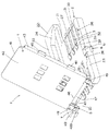
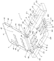
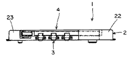
図1、2に示してあるように、実施形態のカード用コネクタ1は、ベースハウジング2と、ベースハウジング2に装着された複数の端子3と、ベースハウジング2に回動可能に設けられたメタルカバー4とを備えている。図3に示してあるように、メタルカバー4は、カード5を一端41から挿入・抜去できるようにされている。
【0015】
ベースハウジング2は、絶縁性のプラスチックで略方形の板状に成形されている。底板21と、底板21の両側縁から立ち上がる側壁22、23を有している。一方の側壁22は、他方の側壁23より長くされて前方に突出している。突出部分221には斜めの極性決め壁24が設けられている。各側壁22、23の後端は、底板21の後方に若干突出し、内側面にヒンジピン25が互いに対向するように設けられている。このヒンジピン25は、側壁22、23に一体となって成形されているが、金属ピンを後から植設するようにすることもできる。
【0016】
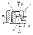
底板21の表面211側で対向している側壁22、23の内側面には、側壁22、23の高さ方向に形成された縦溝261と、縦溝261の下部に略直角となって前方に連続する横溝262でなる切欠凹所26が形成されている。この切欠凹所26は、各側壁22、23に対して2箇所ずつ間隔をおいて形成されている。各側壁22、23に形成された2つの切欠凹所26のうち、前方の切欠凹所26の横溝262は、上部が側壁22、23の肉部222、231で塞がれている。これに対して、後方の切欠凹所26の横溝262は、上部が側壁22、23に装着した金属製のネール6に一体に形成した係合部61で塞がれている。
【0017】
ベースハウジング2の底板21には、複数の端子装着溝27が所定の位置に形成されて、各端子装着溝27に端子3が一つずつ装着されている。
【0018】
端子3は、薄金属板を打ち抜いて成形されている。ベースハウジング2の端子装着溝27に挿入されて、そこに係合する帯状の装着片31を有している。装着片31からは、一方にコンタクト片32が斜め上方に向かって片持ち梁状に延びている。コンタクト片32の先端部には、弧状に湾曲成形されたコンタクト部321が設けられている。また、装着片31から他方に半田テール33が延びている。装着片31を端子装着溝27に装着すると、コンタクト片32に設けたコンタクト部321が底板21の表面211から上方に突出し、半田テール33が底板21の裏面212と略面一となるようにしている。
【0019】
ベースハウジング2の底板21の表面211から突出するようにしたコンタクト部321は、カード5の接点パッド52と1対1の関係で対向できる配置とされている。
【0020】
メタルカバー4は、比較的厚い金属板を打ち抜いて成形されている。方形板状の本体部42の両側に側板43が略直角に連続している。各側板43の端縁から内側に、いくつかの折り返し片44が略直角に連続している。このようにして、本体部42の内側に形成されたカード収容空洞45に、一端41からカード5を挿入し(図3)、また、カード5を抜去できるようにしてある。本体部42の他端46には、ストッパ壁47が設けられている。カード収容空洞45に挿入したカード5の先端面がこのストッパ壁47に当たって、挿入が停止できるようにしてある。
【0021】
メタルカバー4の両側壁43には、方形板状の係合突片48が外向きに突出して設けられている。係合突片48と本体部42は板面が略平行である。係合突片48は、各側板43に2個ずつ設けられている。前記ベースハウジング2の側壁22、23に設けた切欠凹所26の縦溝261の間隔に合わせて設けられている。
【0022】
更に、メタルカバー4の他端46側の両側に、それぞれ一対のヒンジプレート49が、メタルカバー4の延長方向で設けられている。互いに対向しているヒンジプレート49の一方は、本体部42から直接連続して延びている。他方のヒンジプレート49は、側板43から内側に折り曲げられた連続板50(図2)から延びている。
【0023】
各対のヒンジプレート49は、図1と図4〜6及び図10、11に表れているように、中間部に湾曲部491が互いに離れる方向で形成されている。また、湾曲部491より先端側に隣接させて、互いに離れる方向に傾斜するテーパ部492が形成されている。湾曲部491より基端側は、略平行となって対向するようにされている。このようにして、対向する湾曲部491の部分で軸受部分7が構成され、そして、対向するテーパ部492の部分で開放係合部分8が構成されている。
【0024】
ヒンジプレート49で構成された軸受部分7が、ベースハウジング2の側壁22、23の内面から突出させたヒンジピン25に嵌められて、ヒンジ機構が構成され、メタルカバー4がベースハウジング2に対して回動可能に連結されている。メタルカバー4の回動の様子が図4に示されている。メタルカバー4は、矢示Aの方向で回動することができる。この図では、回動したメタルカバー4のいくつかの姿勢が、鎖線と実線で表されている。実際の使用では、実線で示されている位置と、ベースハウジング2の上に重なる位置の範囲で回動する程度である。
【0025】
以上のように構成されている実施形態のカード用コネクタ1にカード5を挿入して接続する操作を説明する前に、このカード用コネクタ1が如何に苛酷な使用に耐えるかについて説明する。
【0026】
苛酷な使用は、メタルカバー4に挿入されたカード5を抜去する際に最も起こりやすい。カード5の抜去は、図4に実線で示した如くの位置にメタルカバー4をカード5と共に回動させ、メタルカバー4の一端41から突出しているカード5の縁51の部分を指で摘んで、矢示Bのように引き抜くようにすればよい。この際に、誤って、メタルカバー4も一緒に引っ張られる事態が想定される。このようにメタルカバー4もカード5の抜去方向(矢示B)に引っ張られた場合、実施形態のカード用コネクタ1では、ヒンジ機構の係合を解除し、メタルカバー4とベースハウジング2を分離させ、ヒンジ機構を破壊から守ることができる。また、場合によってはカード5をメタルカバー4と共にベースハウジング2から離れる方向へ一気に回動させて抜去しようとした際には、結果的にメタルカバー4が前記の実際の使用範囲である実線で示した位置を超えて鎖線で示す位置まで瞬時に回動することになり、これによってメタルカバー4と、メタルカバー4に対向するヒンジプレート25によって挟み込まれているヒンジピン25に大きな負荷が加わってピンが変形したり、メタルカバー4自体が変形してしまう事態も想定される。このようにメタルカバー4に瞬発的な回動に伴う負荷がかかった場合でも、同様にカードコネクタ1ではヒンジ機構の係合を瞬時に解除し、メタルカバー4とベースハウジング2を分離させることによって、特にヒンジピン25を含めたヒンジ機構、及びメタルカバー4自体の破壊を防ぐことができる。
【0027】
即ち、メタルカバー4がカード5の抜去方向に引っ張られると、軸受部分7を構成した、対向するヒンジプレート49が弾性変形して軸受部分7を開き、ヒンジピン25は隣接する開放係合部分8を通して外部に脱出することができる。分離したメタルカバー4は、ヒンジプレート49の開放係合部分8を通して軸受部分7にヒンジピン25を再び嵌めることが可能で、メタルカバー4を元の回動可能の状態に簡単に復帰させることができる。
【0028】
次に、カード5の接続について説明する。接続は、メタルカバー4を図4に実線で示した如くの位置に回動させ、一端41からカード収容空洞45内へカード5を挿入し、次いで、メタルカバー4をカード5と共にベースハウジング2側へ回動して、ベースハウジング2の上に重なるようにして行う。図5は、メタルカバー4がベースハウジング2の上に重なった状態の断面を示している。メタルカバー4がベースハウジング2の上に重なると、カード5の接点パッド52は端子3のコンタクト部321に当接して押し下げ、そして、コンタクト片32を弾性変形させて、その弾性反力で、コンタクト部321と接点パッド52の間に適切な当接圧を形成する。この時、メタルカバー4の両側板43はベースハウジング2の側壁22、23の内側に沿うように位置する。
【0029】
ベースハウジング2の上に重なったメタルカバー4は、ベースハウジング2上で、側壁22、23に沿って、図6の矢示Cのように、スライドさせることができる。矢示Cの方向にメタルカバー4をスライドさせることで、メタルカバー4はベースハウジング2上で、以下に説明するようにしてロックされて、カード5と端子3の接続状態が維持される。メタルカバー4をスライドさせると、接点パッド52がコンタクト部321に当接したままスライドするので、接点パッド52及びコンタクト部321に拭い作用を与えることができる。したがって、接点パッド52とコンタクト部321の電気的な接続を、安定で信頼性の高いものとすることができる。図7〜図9には、メタルカバー4をベースハウジング2の上でスライドさせた後の状態の平面図、左側面図、正面図の三面図が示されている。
【0030】
図7に明らかなように、カード5が、カード収容空洞45に対して表裏を反対にして挿入したり、前後を反対にして挿入する、誤挿入が行われた場合、メタルカバー4をベースハウジング2の上に正しく重なる位置まで回動できないようになっている。切除されていないカード5の角が、極性決め壁24の上に乗るためである。
【0031】
図10及び図11には、ヒンジプレート49を介して設けた軸受部分7及び開放係合部分8とヒンジピン25の係合部分が拡大して示されている。図10は、メタルカバー4をベースハウジング2上でスライドさせる前の状態を表している。軸受部分7とヒンジピン25でヒンジ機構が構成されて、メタルカバー4がヒンジピン25の回りで回動可能であるのは前記の通りである。図11は、メタルカバー4をベースハウジング2上でスライドさせた後の状態を表している。軸受部分7に嵌まっていたヒンジピン25は、開放係合部分8の位置に相対的に移動する。この状態は、2枚のヒンジプレート49の対向するテーパ部492がヒンジピン25を強く挟んでいる。したがって、メタルカバー4には、矢示Cの方向への付勢力が働くことになる。このため、メタルカバー4には、スライドさせてロックした状態を維持するように働き、接点パッド52とコンタクト部321の接続状態を安定に保持することができる。
【0032】
図12及び図13には、メタルカバー4の側板43から突出している係合突片48と、ベースハウジング2の側壁22、23に設けた切欠凹所26の部分が拡大して示されている。図12は、メタルカバー4をベースハウジング2上でスライドさせる前の状態を表している。係合突片48と切欠凹所26の縦溝261の位置が合致している。したがって、メタルカバー4を前記の如くベースハウジング2に重なる方向で回動させる時には、縦溝261が係合突片48の通過する突片通路91となり、メタルカバー4がベースハウジング2の上に重なるまで回動することを可能にする。
【0033】
図13は、メタルカバー4をベースハウジング2上でスライドさせた後の状態を表している。係合突片48は、切欠凹所26の横溝262の方向に移動し、一部が横溝262の上部を仕切っている肉部231(222)と回動方向で係合する。この係合によってメタルカバー4がベースハウジング2から離れる方向への回動及び浮き上がりがロックされる。係合突片48が係合する側壁22、23の肉部222、231は、回動規制壁92となって、前記突片通路91とで係合突片48に対するスライド係合部9を構成している。
【0034】
図14及び図15には、ネール6を設置した切欠凹所26と係合突片48の部分が拡大して示されている。図14がメタルカバー4のスライド前、図15がスライド後の状態である。この切欠凹所26においても、縦溝261は、前記と同様に、係合突片48に対する回動時の突片通路91を構成している。メタルカバー4をスライドさせると、係合突片48の一部は、横溝262の上部を塞いだネール6の係合部61と係合するようになってロックされる。ここでは、ネール6の係合部61が回動規制壁92となって、突片通路91とでスライド係合部9を構成している。
【0035】
回動規制壁92を構成したネール6の係合部61は、図16のように、断面を横U字状に形成されて、下側の係合板611が、係合突片48と係合するようにしている。また、係合板611には、図16に表れているように、係合突片48側に突出する小突起612が設けられ、係合突片48との間で電気的な接触が確実に形成できるようにされている。
【0036】
ネール6の係合板611と、メタルカバー4の係合突片48をこのように電気的な接触を形成するように係合させることによって、静電気の除去回路を形成することができる。メタルカバー4を操作する際、特に、カード5の挿入の際に、操作者の指先からメタルカバー4に流れる静電気をネール6を通してグランド回路に逃がし、携帯電話機等の筐体側の基板回路を保護することが可能である。
【0037】
接続したカード5の取り出しは、メタルカバー4を上記の矢示Cと反対の方向へスライドさせてロックを解除し、次いで、メタルカバー4をベースハウジング2から離れる方向に回動させて行うことができる。
【0038】
【発明の効果】
以上に説明したように、この発明によれば、ベースハウジングとメタルカバーを回動可能に連結したヒンジ機構をメタルカバーの延長方向で分離できる構成としたので、苛酷な取り扱いを受けても破壊しないカード用コネクタを提供することができる。またメタルカバーの係合突片とネールの係合板とを電気的な接触を形成するように係合させることによって、静電気の除去回路を形成し、筐体側の基板回路を保護することができる。
【図面の簡単な説明】
【図1】この発明の実施形態のカード用コネクタの後方から見た斜視図である。
【図2】同じく、実施形態のカード用コネクタの前方から見た斜視図である。
【図3】同じく、実施形態のカード用コネクタの前方から見た斜視図で、SIMカードを挿入した状態の図である。
【図4】同じく、実施形態のカード用コネクタの縦断面図で、メタルカバーを回動する状態の図である。
【図5】同じく、実施形態のカード用コネクタの縦断面図で、メタルカバーを回動してハウジングの上に重なった状態の図である。
【図6】同じく、実施形態のカード用コネクタの縦断面図で、メタルカバースライドさせた状態の図である。
【図7】実施形態のカード用コネクタの、メタルカバースライドさせた状態の平面図である。
【図8】同じく、実施形態のカード用コネクタの、メタルカバースライドさせた状態の左側面図である。
【図9】同じく、実施形態のカード用コネクタの、メタルカバースライドさせた状態の正面図である。
【図10】図5のK部の拡大断面図である。
【図11】図6のL部の拡大断面図である。
【図12】図7のM部の拡大平面図で、メタルカバーをスライドさせる前の状態の図である。
【図13】同じく、図7のM部の拡大平面図で、メタルカバーをスライドさせた後の状態の図である。
【図14】図7のN部の拡大平面図で、メタルカバーをスライドさせる前の状態の図である。
【図15】同じく、図7のN部の拡大平面図で、メタルカバーをスライドさせた後の状態の図である。
【図16】図15のO−O線に沿って示した拡大断面図である。
【符号の説明】
1 カード用コネクタ
2 ベースハウジング
21 底板
211 表面
212 裏面
22 側壁
221 突出部分
222 肉部
23 側壁
231 肉部
24 極性決め壁
25 ヒンジピン
26 スライド係合部
261 縦溝
262 横溝
27 端子装着溝
3 端子
31 装着片
32 コンタクト片
321 コンタクト部
33 半田テール
4 メタルカバー
41 一端
42 本体部
43 側板
44 折り返し片
45 カード収容空洞
46 他端
47 ストッパ壁
48 係合突片
49 ヒンジプレート
491 湾曲部
492 テーパ部
50 連続板
5 カード
51 縁
52 接点パッド
6 ネール
61 係合部
611 係合板
612 小突起
7 軸受部分
8 開放係合部分
9 スライド係合部
91 突片通路
92 回動規制壁[0001]
TECHNICAL FIELD OF THE INVENTION
The present invention relates to a card connector for connecting a card such as a SIM (Subscriber Identity Module) card used in a mobile phone.
[0002]
[Prior art]
2. Description of the Related Art Conventionally, as a card connector of this type, there is a card connector including a base housing on which a plurality of terminals are mounted and a cover rotatably provided on the base housing. For example, it is shown in FIG. 1 of Japanese Patent No. 3086209. In the figure, 18 is a base housing, 20 is a cover, and 28 is a terminal. Further, similar ones are disclosed in Japanese Patent No. 3092069, Utility Model Registration No. 3078227, and Japanese Utility Model Application Laid-Open No. 62-47019.
[0003]
The terminal mounted on the base housing is provided with an elastic contact piece so that a contact portion formed on the contact piece projects from the surface of the base housing. The card can be inserted and removed from one end of the cover. After the card is inserted into the cover, the cover is rotated so as to overlap the base housing, so that the contact pads provided on the card and the contact portions of the terminals resiliently contact each other so as to be electrically connected.
[0004]
In order to make the cover rotatable with respect to the base housing, a hinge mechanism is configured between the other end of the cover (the end opposite to the end where the card is inserted) and the base housing. Usually, this hinge mechanism is configured such that a hinge pin is provided on one of a base housing and a cover, and a bearing portion is provided on the other, so that they are fitted to each other. The card connector disclosed in Japanese Patent No. 3086209 is different from the card connector in that an L-shaped cross section is provided at the end of the base 18 so that the pin accommodating recesses 46a and 46b are adjacent to each other. The pivot pin 44 (FIG. 10) of the cover 20 is engaged with the pin receiving recess. The cover 20 can move (slide) on the base 18 (see paragraphs [0024] and [0027]).
[0005]
[Problems to be solved by the invention]
By the way, the user who uses the card connector having such a configuration is not usually familiar with the structure of the card connector and the handling method. This is particularly noticeable for mobile phone users. For example, when removing the card (SIM card) from the cover, the card may be pulled out of the cover together with the card, or the card may be rotated with the metal cover at a stretch to remove the card. If such unreasonable handling is received, the hinge mechanism and the like provided between the base and the cover will be broken, and the replacement of the card connector will be forced. Therefore, a card connector having a structure capable of withstanding severe handling is desired.
[0006]
The present invention has been made in view of such circumstances, and an object of the present invention is to provide a card connector that does not break even when subjected to severe handling.
[0007]
[Means for Solving the Problems]
A card connector of the present invention made for the above purpose has a base housing formed into a substantially rectangular plate shape,
A metal cover that allows the card to be inserted and removed from one end,
A plurality of terminals mounted on the base housing, the contact portions protruding from the surface of the base housing,
On the other end side of the metal cover, two hinge plates facing each other are provided in the extension direction of the metal cover, and a curved portion is formed in a middle portion of each hinge plate in a direction away from each other. A bearing portion is configured, and an open engagement portion is configured adjacent to the bearing portion,
A card connector characterized in that the bearing portion composed of two hinge plates is fitted to a hinge pin provided in the base housing, and a metal cover is rotatably connected to the base housing. is there.
[0008]
[Action]
According to the card connector of the present invention configured as described above, the hinge plate is provided in the extension direction of the metal cover, and the bearing portion formed via the hinge plate is fitted to the hinge pin on the base housing side. Therefore, if the metal cover is pulled out in the card removal direction, or if the metal cover is swiveled in a direction away from the base housing together with the card at a stretch, the hinge pin will move from the bearing part to the outside through the open engagement part. You can escape. That is, the engagement of the hinge mechanism formed by fitting the hinge pin and the bearing portion is released, and the metal cover can be separated from the base housing. Therefore, even if the metal cover is forcibly handled, the hinge mechanism can be prevented from being broken.
[0009]
It is desirable to provide at least one pair of hinge plates on each side of the other end of the metal cover. When the hinge plate pair is provided on each side as described above, a side wall is provided on the base housing side, and a hinge pin is projected from the side wall, so that a hinge mechanism can be easily formed between the hinge plate and the hinge plate.
[0010]
The side wall provided on the base housing is desirably provided along the outside of the metal cover. An engaging projection is provided on the side edge of the metal cover so as to protrude outward.On the side wall on the base housing side, a projection passage through which the engaging projection can pass when the metal cover is rotated, A slide engagement portion is provided by the engagement protrusion and the rotation restricting wall that is engaged in the rotation direction. With such a configuration, when the metal cover is rotated so as to overlap the base housing, the metal cover is slid along the base housing so that the engagement protrusion and the rotation restricting wall are engaged in the rotation direction. In this manner, the metal cover overlapping the base housing can be held at that position.
[0011]
When the metal cover is slid along the base housing, the hinge pin fitted on the bearing portion of the hinge plate relatively moves to the open engagement portion and engages at the portion. If this open engagement portion is configured such that a tapered portion provided at the distal end portion of the hinge plate faces each other and is gradually opened toward the distal end, the metal cover is pushed through the tapered portion and the engagement is performed. The engagement between the projection and the rotation restricting wall can be prevented from being disengaged.
[0012]
Nail to be soldered to the mounting board can be mounted on the side wall of the base housing. Then, when the rotation restricting wall of the slide engaging portion is constituted by the engaging portion extending from the nail, after the metal cover slides, the engaging protruding piece of the metal cover and the engaging plate of the nail come into contact with each other so that the metal cover and the nail are separated. Electrical continuity can be formed to form a circuit for removing static electricity.
[0013]
BEST MODE FOR CARRYING OUT THE INVENTION
Hereinafter, embodiments of the present invention will be described with reference to the accompanying drawings.
[0014]
As shown in FIGS. 1 and 2, the card connector 1 according to the embodiment includes a
[0015]
The
[0016]
On the inner surfaces of the
[0017]
A plurality of
[0018]
The
[0019]
The
[0020]
The
[0021]
On both
[0022]
Further, a pair of
[0023]
As shown in FIGS. 1 and 4 to 6 and FIGS. 10 and 11, each pair of
[0024]
The bearing
[0025]
Before describing the operation of inserting and connecting the
[0026]
Severe use is most likely to occur when removing the
[0027]
That is, when the
[0028]
Next, connection of the
[0029]
The
[0030]
As is clear from FIG. 7, when the
[0031]
FIGS. 10 and 11 show an enlarged view of an engagement portion between the bearing
[0032]
FIG. 12 and FIG. 13 show, in an enlarged manner, a portion of an engaging
[0033]
FIG. 13 shows a state after the
[0034]
FIGS. 14 and 15 show the
[0035]
As shown in FIG. 16, the engaging
[0036]
By engaging the engagement plate 611 of the
[0037]
The removal of the
[0038]
【The invention's effect】
As described above, according to the present invention, the hinge mechanism that rotatably connects the base housing and the metal cover is configured to be separable in the extension direction of the metal cover, so that the hinge mechanism is not broken even when subjected to severe handling. A card connector can be provided. Further, by engaging the engaging projection of the metal cover with the engaging plate of the nail so as to form an electrical contact, a static electricity removing circuit can be formed, and the substrate circuit on the housing side can be protected.
[Brief description of the drawings]
FIG. 1 is a perspective view of a card connector according to an embodiment of the present invention as viewed from the rear.
FIG. 2 is a perspective view of the card connector of the embodiment as viewed from the front.
FIG. 3 is a perspective view of the card connector of the embodiment as viewed from the front, with a SIM card inserted.
FIG. 4 is a vertical sectional view of the card connector of the embodiment, showing a state in which a metal cover is rotated.
FIG. 5 is a longitudinal sectional view of the card connector of the embodiment, showing a state in which the metal cover is turned and overlapped on the housing.
FIG. 6 is a longitudinal sectional view of the card connector of the embodiment, showing a state in which a metal cover is slid.
FIG. 7 is a plan view of the card connector of the embodiment in a state where a metal cover is slid.
FIG. 8 is a left side view of the card connector of the embodiment, with a metal cover slid.
FIG. 9 is a front view of the card connector of the embodiment in a state where a metal cover is slid.
FIG. 10 is an enlarged sectional view of a portion K in FIG. 5;
FIG. 11 is an enlarged sectional view of a portion L in FIG. 6;
FIG. 12 is an enlarged plan view of a portion M in FIG. 7, showing a state before a metal cover is slid.
13 is an enlarged plan view of a portion M in FIG. 7, showing a state after a metal cover is slid.
FIG. 14 is an enlarged plan view of a portion N in FIG. 7, showing a state before a metal cover is slid.
FIG. 15 is an enlarged plan view of a portion N in FIG. 7, showing a state after the metal cover is slid.
FIG. 16 is an enlarged sectional view taken along line OO of FIG. 15;
[Explanation of symbols]
DESCRIPTION OF SYMBOLS 1
Claims (4)
カード(5)を一端(41)から挿入・抜去可能にしたメタルカバー(4)と、
前記ベースハウジング(2)に装着され、コンタクト部(321)がベースハウジング(2)の表面(211)から突出している複数の端子(3)とを備えており、
前記メタルカバー(4)の他端(46)側に、互いに対向する少なくとも一対のヒンジプレート(49)がメタルカバー(4)の延長方向で設けられ、各ヒンジプレート(49)の中間部に、互いに離れる方向で湾曲部(491)が形成され、対向する湾曲部(491)で軸受部分(7)が構成されていると共に、軸受部分(7)に隣接して開放係合部分(8)が構成されており、
2枚のヒンジプレート(49)で構成された前記軸受部分(7)を前記ベースハウジング(2)に設けられたヒンジピン(25)に嵌めて、ベースハウジング(2)に対してメタルカバー(4)が回動可能に連結されていることを特徴とするカード用コネクタ。A base housing (2) formed into a substantially rectangular plate shape,
A metal cover (4) that allows the card (5) to be inserted and withdrawn from one end (41);
A plurality of terminals (3) mounted on the base housing (2) and having a contact portion (321) protruding from a surface (211) of the base housing (2);
At least one pair of hinge plates (49) facing each other is provided on the other end (46) side of the metal cover (4) in the extending direction of the metal cover (4). A curved portion (491) is formed in a direction away from each other, a bearing portion (7) is constituted by the opposed curved portion (491), and an open engagement portion (8) is formed adjacent to the bearing portion (7). Is composed of
The bearing portion (7) constituted by two hinge plates (49) is fitted to a hinge pin (25) provided on the base housing (2), and the metal cover (4) is attached to the base housing (2). Wherein the connector is rotatably connected.
Priority Applications (1)
| Application Number | Priority Date | Filing Date | Title |
|---|---|---|---|
| JP2002376342A JP2004207104A (en) | 2002-12-26 | 2002-12-26 | Card connector |
Applications Claiming Priority (1)
| Application Number | Priority Date | Filing Date | Title |
|---|---|---|---|
| JP2002376342A JP2004207104A (en) | 2002-12-26 | 2002-12-26 | Card connector |
Publications (1)
| Publication Number | Publication Date |
|---|---|
| JP2004207104A true JP2004207104A (en) | 2004-07-22 |
Family
ID=32813832
Family Applications (1)
| Application Number | Title | Priority Date | Filing Date |
|---|---|---|---|
| JP2002376342A Pending JP2004207104A (en) | 2002-12-26 | 2002-12-26 | Card connector |
Country Status (1)
| Country | Link |
|---|---|
| JP (1) | JP2004207104A (en) |
Cited By (6)
| Publication number | Priority date | Publication date | Assignee | Title |
|---|---|---|---|---|
| JP2006210127A (en) * | 2005-01-27 | 2006-08-10 | Jst Mfg Co Ltd | Card connector |
| JP2006210128A (en) * | 2005-01-27 | 2006-08-10 | Jst Mfg Co Ltd | Card connector |
| CN100416926C (en) * | 2005-01-27 | 2008-09-03 | 日本压着端子制造株式会社 | Card connector |
| JP2008305787A (en) * | 2007-06-08 | 2008-12-18 | Mea Technologies Pte Ltd | Connector for card |
| JP2008305786A (en) * | 2007-06-08 | 2008-12-18 | Mea Technologies Pte Ltd | Connector for card |
| JP2012003920A (en) * | 2010-06-16 | 2012-01-05 | Jst Mfg Co Ltd | Card connector |
-
2002
- 2002-12-26 JP JP2002376342A patent/JP2004207104A/en active Pending
Cited By (8)
| Publication number | Priority date | Publication date | Assignee | Title |
|---|---|---|---|---|
| JP2006210127A (en) * | 2005-01-27 | 2006-08-10 | Jst Mfg Co Ltd | Card connector |
| JP2006210128A (en) * | 2005-01-27 | 2006-08-10 | Jst Mfg Co Ltd | Card connector |
| CN100416926C (en) * | 2005-01-27 | 2008-09-03 | 日本压着端子制造株式会社 | Card connector |
| JP4515928B2 (en) * | 2005-01-27 | 2010-08-04 | 日本圧着端子製造株式会社 | Card connector |
| JP4611041B2 (en) * | 2005-01-27 | 2011-01-12 | 日本圧着端子製造株式会社 | Card connector |
| JP2008305787A (en) * | 2007-06-08 | 2008-12-18 | Mea Technologies Pte Ltd | Connector for card |
| JP2008305786A (en) * | 2007-06-08 | 2008-12-18 | Mea Technologies Pte Ltd | Connector for card |
| JP2012003920A (en) * | 2010-06-16 | 2012-01-05 | Jst Mfg Co Ltd | Card connector |
Similar Documents
| Publication | Publication Date | Title |
|---|---|---|
| CN100388564C (en) | Electrical connector for a smart card, comprising a switch for locking the card-carrying cover | |
| CN203014023U (en) | Pallet used for card and connector used for card | |
| CN101488621B (en) | Cable connector assembly | |
| JP2004288494A (en) | Connector | |
| US6478630B1 (en) | Electrical card connector having polarization mechanism | |
| JP2006209992A (en) | Connector for ic card | |
| JP3711540B2 (en) | Thin connector | |
| JPH10284181A (en) | Electrical connector for card having surface contact | |
| JP2004207104A (en) | Card connector | |
| JP2004127767A (en) | Connector for card | |
| US7234966B2 (en) | IC card connector equipped with respective cover doors and associated anti-mismating device | |
| TWM454643U (en) | Nanometer type electronic card connector | |
| US7503500B2 (en) | Card connector with anti-mismating device | |
| SG188682A1 (en) | Electrical card connector | |
| JP4851667B2 (en) | Card connector | |
| JP3981942B2 (en) | Electrical connector | |
| JP2004127733A (en) | Connector for card | |
| JP2004220787A (en) | Connector for card | |
| JPH0579668U (en) | connector | |
| JP3772788B2 (en) | Card connector | |
| EP1544958B1 (en) | Card connector | |
| JP3932330B2 (en) | Flat conductor connector | |
| JP2016136462A (en) | Electric connector | |
| JP3668924B2 (en) | Battery holder | |
| JP2006100057A (en) | Flexible board for connector |