JP2004200982A - Reader/writer for non-contact ic card - Google Patents
Reader/writer for non-contact ic card Download PDFInfo
- Publication number
- JP2004200982A JP2004200982A JP2002366491A JP2002366491A JP2004200982A JP 2004200982 A JP2004200982 A JP 2004200982A JP 2002366491 A JP2002366491 A JP 2002366491A JP 2002366491 A JP2002366491 A JP 2002366491A JP 2004200982 A JP2004200982 A JP 2004200982A
- Authority
- JP
- Japan
- Prior art keywords
- signal
- circuit
- modulation
- reader
- writer
- Prior art date
- Legal status (The legal status is an assumption and is not a legal conclusion. Google has not performed a legal analysis and makes no representation as to the accuracy of the status listed.)
- Granted
Links
- 230000002194 synthesizing effect Effects 0.000 claims abstract description 5
- 238000000034 method Methods 0.000 claims description 50
- 238000006243 chemical reaction Methods 0.000 claims description 24
- 230000005540 biological transmission Effects 0.000 claims description 21
- 239000002131 composite material Substances 0.000 claims description 3
- 230000006854 communication Effects 0.000 description 13
- 238000004891 communication Methods 0.000 description 13
- 238000010586 diagram Methods 0.000 description 8
- 230000010355 oscillation Effects 0.000 description 3
- 230000001360 synchronised effect Effects 0.000 description 3
- 230000015572 biosynthetic process Effects 0.000 description 2
- 238000004519 manufacturing process Methods 0.000 description 2
- 230000004044 response Effects 0.000 description 2
- 238000003786 synthesis reaction Methods 0.000 description 2
- 230000007175 bidirectional communication Effects 0.000 description 1
- 230000000295 complement effect Effects 0.000 description 1
- 230000008878 coupling Effects 0.000 description 1
- 238000010168 coupling process Methods 0.000 description 1
- 238000005859 coupling reaction Methods 0.000 description 1
- 230000005674 electromagnetic induction Effects 0.000 description 1
Images


Abstract
Description
【0001】
【発明の属する技術分野】
本発明は、相異なる通信方式によりICカードと通信可能な非接触ICカード用リーダライタに関する。
【0002】
【従来の技術】
電磁波の送受信により情報を授受する非接触式の応答ユニットとして、例えば特許文献1に記載したものがある。これは、例えば自動生産ラインにおける移動機などに装着して使用されるものである。これに対し、近年は、事業場用の入門管理システムや自動改札機をはじめとする多くのシステムでICカードが使用されており、それに伴って当該ICカードに対し情報を読み書きするための非接触ICカード用リーダライタが使用されている。
【0003】
【特許文献1】
特開平10−13295号公報
【0004】
【発明が解決しようとする課題】
非接触ICカードには通信距離や通信周波数によってISO規格が制定されており、密着型(ISO10536)、近接型(ISO14443)、近傍型(ISO15693)などの種類がある。このうち近接型非接触ICカードには、データの変調方式によってTYPE−AとTYPE−Bとがある。TYPE−AとTYPE−Bの各方式は、何れもリーダライタからICカードへの送信にASK変調方式を採用している。
【0005】
TYPE−A方式は、一般にCPUが内蔵されてないハードウェアロジックで構成された制御回路を持つ非接触ICカードに利用される方式であり、シンプルなプロトコルをもつICカード用として、例えば個人識別カードやプリペイドカードなどに利用されることが多い。一方、TYPE−B方式は、CPUを内蔵した非接触ICカードで利用される方式であり、比較的複雑なプロトコルをもつ銀行用のキャッシュカードやクレジットカードなどに利用されることが多い。
【0006】
図6は、ISO14443のTYPE−B方式を採用した既存のリーダライタ1における変復調回路部分の電気的構成を示すブロック図である。IC化されている符号化回路2は、CPU3から送られた送信データをNRZ符号に変換したベースバンド信号Sb(B)を生成し、発振回路4から13.56MHzのクロックの供給を受けてキャリア信号Scとともに変調回路5に出力する。変調回路5は、例えば単同調送信方式を採用しており、10%ASK変調方式により変調した信号をアンテナ6を介してICカード7に送信する。一方、復調回路8は、アンテナ6を介して受信した信号を復調し、その復調信号は復号化回路9を介して符号化回路2に入力される。図7は、この構成におけるキャリア信号Sc、ベースバンド信号Sb(B)、アンテナの出力信号Swの各波形を示している。
【0007】
ところで、近年、非接触ICカードの普及に伴い、各種仕様のICカードを統合したコンビネーションカードが提案されている。現在は、メモリ等を共有し通信のインターフェースを非接触近接型と外部端子付きとで使い分けるコンビネーションカードのニーズが高まっているが、その一方で上記TYPE−A方式とTYPE−B方式とのコンビネーションカードも考えられている。両タイプを統合したICカードに対して各変調方式専用のリーダライタを準備することは手間であり、コストの上でも不利となる。そこで、TYPE−A、TYPE−B何れの変調方式でも通信可能なリーダライタの実現が必要となる。
【0008】
例えばTYPE−B方式を採用する図6に示すリーダライタ1にTYPE−A方式を追加する場合、開発期間および開発コストを抑える上で既存のTYPE−A方式の符号化/復号化用ICを組み合わせることが考えられる。しかし、既存の符号化/復号化用ICは、他のICと組み合わせることを前提として設計されていないため、そのまま組み合わせることはできない。
【0009】
すなわち、リーダライタ1の変調回路5は単同調送信方式であるのに対し、TYPE−A方式を採用する他の符号化/復号化用ICは複同調送信方式である。
この送信方式の相違により、両者を単に組み合わせただけではリーダライタにアンテナを2種類搭載する必要が生じ、装置の大型化やコスト高などの問題が生じる。
【0010】
本発明は上記事情に鑑みてなされたもので、その目的は、2つの相異なるASK変調方式の何れでも通信可能であって且つ既存の回路を利用して構成できる非接触ICカード用リーダライタを提供することにある。
【0011】
【課題を解決するための手段】
請求項1に記載した手段によれば、キャリア信号出力回路は、変調選択信号の状態にかかわらずキャリア信号を出力し続ける。変調選択信号が第1の状態である場合に、第1の変換回路は、送信データを第1のASK変調方式に従って符号化した第1のベースバンド信号を出力し、第2の変換回路は、定レベル信号を出力する。このとき、信号合成回路は、キャリア信号と第1のベースバンド信号とを合成するため、キャリア信号の振幅は、2値信号である第1のベースバンド信号に応じて複数段階(例えば0%/100%の2段階)に変化する。つまり、この時点で第1の変調方式による変調がなされたことになる。
【0012】
その結果、変調回路のベースバンド信号入力端子には定レベル信号が入力され、変調回路のキャリア信号入力端子には上記合成信号が入力される。変調回路は、入力されるベースバンド信号が一定レベルであることから、上記第1の変調方式による変調がされた合成信号をそのまま被変調信号として出力する。
【0013】
これに対し、変調選択信号が第2の状態である場合に、第1の変換回路は、定レベル信号を出力し、第2の変換回路は、送信データを第2のASK変調方式に従って変換した第2のベースバンド信号を出力する。このとき、信号合成回路は、キャリア信号と定レベル信号とを合成するため、キャリア信号をそのまま出力する。これにより、変調回路のベースバンド信号入力端子には第2のベースバンド信号が入力され、変調回路のキャリア信号入力端子にはキャリア信号が入力される。変調回路は、本来のASK変調動作に従って、第2の変調方式に従った被変調信号を出力する。
【0014】
従って、当該非接触ICカード用リーダライタによれば、単一の変調回路を備えているにもかかわらず、変調選択信号の状態を切り替えることにより相異なる2種類のASK変調方式の何れでも通信可能となる。これにより、複数種類のICカードに対して情報の読み書きが可能となる。また、第1、第2の変換回路とは、互いに協調動作するように特別な設計がされている必要はなく、既存の符号化/復号化用回路を利用することができる。
【0015】
請求項2に記載した手段によれば、信号合成回路はAND回路から構成されているので、合成信号は、第1のベースバンド信号がハイレベルのときにキャリア信号に等しくなり、第1のベースバンド信号がロウレベルのときにロウレベル一定となる。つまり、合成信号は、第1のベースバンド信号により100%ASK変調が施された信号となる。
【0016】
請求項3に記載した手段によれば、単一のアンテナにより受信した受信信号が分配されて、その分配された受信信号が、それぞれ第1の変換回路と組み合わせて用いられる第1の復調回路および第2の変換回路と組み合わせて用いられる第2の復調回路に入力されるため、ICカードと当該非接触ICカード用リーダライタとの間で双方向の通信が可能となる。ICカードから非接触ICカード用リーダライタへの通信方式は、例えば負荷変調方式である。
【0017】
請求項4に記載した手段によれば、第1の変換回路と第1の復調回路およびキャリア信号出力回路と第2の変換回路がそれぞれ1つのICとして構成されている。この形態は、現在用いられている通信用ICの形態の一つである。本願発明は、こうした既存のICを利用して、2種類の変調方式の何れによってもICカードとの通信を可能としたもので、新たなICを新規に開発する手間とコストを省くことができる。
【0018】
請求項5に記載した手段によれば、第1と第2の変換回路は、共通のクロックに基づいて動作するので、容易にキャリア信号と第1、第2のベースバンド信号との同期をとることができる。
【0019】
請求項6に記載した手段によれば、第1の変調方式は100%ASK変調方式であり、第2の変調方式は10%ASK変調方式であるため、ISO14443により制定された近接型非接触ICカードとの通信に適用できる。
【0020】
【発明の実施の形態】
以下、本発明の一実施形態について図1ないし図5を参照しながら説明する。
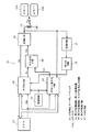
図1は、ICカード用リーダライタにおいて変復調回路部分の電気的構成を示すブロック図である。このICカード用リーダライタ11(以下、単にリーダライタ11と称す)は、ISO14443の規格により定められた近接型非接触ICカード12A、12Bとの間で通信を行うものである。ISO14443には、TYPE−A(ICカード12Aに対応)とTYPE−B(ICカード12Bに対応)の通信方式が規定されており、リーダライタ11は両方式の何れを用いても通信可能である点に特徴を有している。
【0021】
リーダライタ11からICカード送信する場合、TYPE−A方式は、キャリア信号(fc=13.56MHz)の振幅が0%と100%の組み合わせによりデータ「0」と「1」を表わす100%ASK(Amplitude Shift Keying)変調方式を採用している。一方、TYPE−B方式は、キャリア信号(fc=13.56MHz)の振幅が90%と100%の組み合わせによりデータ「0」と「1」を表わす10%ASK変調方式を採用している。
【0022】
また、ICカード12A、12Bからリーダライタ11に送信する場合、TYPE−A方式、TYPE−B方式の何れにおいても、ICカード12A、12Bは、キャリア信号(搬送波)を副搬送波の周波数(fc/16=847kHz)で負荷変調することによって、磁気結合の間隙を介してリーダライタ11に送信するようになっている。
【0023】
リーダライタ11にはパソコンなどの上位装置(図示せず)が接続されており、CPU13は、当該上位装置から送られてくるカード選択信号に応じて、変調選択信号Smを出力するようになっている。リーダライタ11は、変調選択信号Smがハイレベルの場合にTYPE−A方式のICカード12Aと通信を行い、変調選択信号Smがロウレベルの場合にTYPE−B方式のICカード12Bと通信を行うようになっている。
【0024】
符号化/復号化回路14(第1の変換回路、第1の復調回路に相当)は、TYPE−A方式に基づいてCPU13の送受信データとベースバンド信号Sb(A)との間の符号化/復号化および復調を行うもので、一つのICとして構成されている。変調選択信号Smがハイレベルの場合、ICカード12Aへの送信については、CPU13からの送信データを変形ミラー符号化方式によりベースバンド信号Sb(A)に変換して出力し、ICカード12Aからの受信については、アンテナ16からの受信信号を復調した後OOK−マンチェスタ符号化方式により受信データの復号化を行うようになっている。一方、変調選択信号Smがロウレベルの場合には、上記ベースバンド信号Sb(A)に替えてハイレベル一定の定レベル信号を出力するようになっている。
【0025】
これに対し、符号化回路15(第2の変換回路に相当)は、TYPE−B方式に基づいてCPU13の送信データとベースバンド信号Sb(B)との間の符号化を行うもので、一つのICとして構成されている。変調選択信号Smがロウレベルの場合、ICカード12Bへの送信については、CPU13からの送信データをNRZ符号化方式によりベースバンド信号Sb(B)に変換して出力し、変調選択信号Smがハイレベルの場合、上記ベースバンド信号Sb(B)に替えてハイレベル一定の定レベル信号を出力するようになっている。
【0026】
また、ICカード12Bからの受信については、アンテナ16からの受信信号を復号化する復調回路17(第2の復調回路に相当)と、BPSK−NRZ符号化方式により受信データを復号化する復号化回路18とによって行われるようになっている。この受信データは、符号化回路15を介してCPU13に送られるようになっている。
【0027】
なお、符号化/復号化回路14、符号化回路15を構成する各ICは既存のものである。従って、実際の変調選択信号Smは、CPU13から各ICに送られる動作許可信号を相補的な信号とすることにより実現されている。すなわち、CPU13から符号化/復号化回路14に対してのみ動作許可信号を出力した状態が、TYPE−A方式を選択するための変調選択信号の第1の状態(上記ハイレベルの状態)に相当し、CPU13から符号化回路15に対してのみ動作許可信号を出力した状態がTYPE−B方式を選択するための変調選択信号の第2の状態(上記ロウレベルの状態)に相当する。
【0028】
符号化/復号化回路14、符号化回路15を構成する各ICには、発振回路19から共通のクロックが入力されるようになっており、キャリア信号出力回路として機能する符号化回路15は、fc(=13.56MHz)のキャリア信号Scを出力するようになっている。これにより、ベースバンド信号Sb(A) 、Sb(B) とキャリア信号Scとの同期がとられるようになっている。
【0029】
信号合成回路20は、具体的にはAND回路から構成されており、符号化回路15からのキャリア信号Scと符号化/復号化回路14の出力信号SAとの論理積である合成信号Sdを出力するようになっている。
【0030】
変調回路21は、単一のキャリア信号入力端子とベースバンド信号入力端子とを有し、TYPE−B方式の変調を行う回路である。ベースバンド信号入力端子には、符号化回路15の出力信号SB(すなわちベースバンド信号Sb(B)または定レベル信号)が入力され、キャリア信号入力端子には信号合成回路20からの合成信号Sdが入力されるようになっている。この変調回路21の出力端子は、アンテナ16に接続されている。アンテナ16を介して受信された信号は2系統に分配され、一方が符号化/復号化回路14に直接入力され、他方が復調回路17に入力されるようになっている。なお、アンテナ16とICカード12A、12Bのアンテナとの間は電磁誘導により結合されるようになっている。
【0031】
次に、本実施形態の作用について図2ないし図5も参照しながら説明する。
図2は、リーダライタ11からTYPE−A方式のICカード12Aに送信する場合の各部の信号波形を示し、図3は、リーダライタ11からTYPE−B方式のICカード12Bに送信する場合の各部の信号波形を示している。各波形は以下の通りである。
【0032】
(a)符号化回路15から出力されるキャリア信号Sc
(b)符号化/復号化回路14の出力信号SA
(c)符号化回路15の出力信号SB
(d)信号合成回路20から出力される合成信号Sd
(e)アンテナ16の出力信号Sw
【0033】
図2に示す場合には、変調選択信号Smはハイレベルとなっている。そこで、符号化/復号化回路14は、送信データを変形ミラー符号化方式によりベースバンド信号Sb(A)に変換してそれを出力信号SAとして出力し、符号化回路15は、ハイレベル一定の定レベル信号を出力信号SBとして出力する。信号合成回路20は、キャリア信号Scとベースバンド信号Sb(A)との論理積により、キャリア信号Scについてベースバンド信号Sb(A)がロウレベルの時に振幅0%、ベースバンド信号Sb(A)がハイレベルの時に振幅100%となる合成信号Sdを出力する。この合成信号Sdは、キャリア信号Scをベースバンド信号Sb(A)で100%ASK変調した信号となっている。
【0034】
TYPE−B方式の変調を行う変調回路21は、ベースバンド信号入力端子の信号がハイレベルの時にキャリア信号入力端子の信号を100%の振幅で出力するため、出力信号SBがハイレベルの定レベル信号である本ケースでは、合成信号Sdをそのまま出力する。これにより、アンテナ16からは、TYPE−A方式である100%ASK変調された出力信号Swが出力される。
【0035】
これに対し、図3に示す場合には、変調選択信号Smはロウレベルとなっている。そこで、符号化回路15は、送信データをNRZ符号化方式によりベースバンド信号Sb(B)に変換してそれを出力信号SBとして出力し、符号化/復号化回路14は、ハイレベル一定の定レベル信号を出力信号SAとして出力する。信号合成回路20は、キャリア信号Scとハイレベルの定レベル信号との論理積により、キャリア信号Scに等しい合成信号Sdを出力する。
【0036】
従って、変調回路21は、符号化回路15から出力されたベースバンド信号Sb(B)とキャリア信号Scとがそのまま入力された場合と同じ動作となり、ベースバンド信号Sb(B)に対しTYPE−B方式の10%ASK変調を行ってアンテナ16を介して出力信号Swを出力する。
【0037】
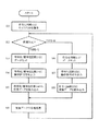
次に、リーダライタ11がICカード12Aまたは12Bと通信する場合の一連の動作内容について説明する。図4は、CPU13の処理内容を示すフローチャートである。CPU13は、まずステップS1において符号化回路15に対しキャリアONを指令する。続いて、ステップS2において、パソコンなどの上位装置からのカード選択信号に基づいて、適用すべき変調方式がTYPE−A方式であるかTYPE−B方式であるかを判断する。ここで、ICカード12Aのカード選択信号を受けた場合には、TYPE−A方式を適用すると判断してステップS3に移行する。
【0038】
CPU13は、ステップS3において符号化/復号化回路14に送信データをセットし、ステップS4において符号化/復号化回路14に対して動作許可信号を出力する。これにより、変調選択信号Smがハイレベルの状態となり、符号化/復号化回路14はベースバンド信号Sb(A)を出力し、符号化回路15はハイレベルの定レベル信号を出力する。その結果、上述したように変調回路21からアンテナ16を介してTYPE−A方式による出力信号Swが出力される。
【0039】
ICカード12Aは、搬送波を副搬送波の周波数で負荷変調することによってリーダライタ11と通信する。アンテナ16により受信された信号は符号化/復号化回路14に直接入力され、そこで復調および復号化が行われて受信データが得られる。CPU13は、ステップS5において、符号化/復号化回路14から受信データを読み込む。
【0040】
一方、ICカード12Bとの通信を行う場合には、上記ステップS2においてTYPE−B方式を適用すると判断してステップS6に移行する。CPU13は、ステップS6において符号化回路15に送信データをセットし、ステップS7において符号化回路15に対して動作許可信号を出力する。これにより、変調選択信号Smがロウレベルの状態となり、符号化回路15はベースバンド信号Sb(B)を出力し、符号化/復号化回路14はハイレベルの定レベル信号を出力する。その結果、上述したように変調回路21からアンテナ16を介してTYPE−B方式による出力信号Swが出力される。
【0041】
ICカード12Bも負荷変調することによってリーダライタ11と通信する。
アンテナ16により受信された信号は、復調回路17で復調され、復号化回路18で復号化され、得られた受信データが符号化回路15にセットされる。CPU13は、ステップS8において符号化回路15から受信データを読み込む。その後、CPU13は、ステップS9において、読み込んだ受信データについて処理を行う。
【0042】
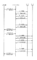
図5は、リーダライタ11を用いてICカード12A、12Bと通信する場合のシーケンス図である。ここでは、まず初めにICカード12Aと通信し、その後ICカード12Bと通信する場合を示している。パソコンなどの上位装置からリーダライタ11にTYPE−Aのカード選択信号が送信されると、リーダライタ11とICカード12Aとの間でデータの送信とそれに対する応答が必要回数だけ繰り返される。そして、リーダライタ11とICカード12Aとの間の通信が完了すると、リーダライタ11から上位装置に対し、処理完了信号が送信される。上位装置は、処理完了信号を受信すると、新たに要求されたカード選択信号(図5ではTYPE−Bの選択)をリーダライタ11に送信し、リーダライタ11は、上述と同様にして要求されたTYPE−BのICカード12Bとの間で通信を行う。
【0043】
以上説明したように、本実施形態のリーダライタ11は、変調方式ISO14443のTYPE−A、TYPE−Bの符号化を行う既存の符号化/復号化回路14、符号化回路15とともに、符号化/復号化回路14の出力信号SAとキャリア信号Scとの合成信号Sdを生成する信号合成回路20を備えている。これにより、TYPE−A方式の変調回路を備えることなくTYPE−B方式の変調を行う既存の変調回路21を備えるだけで、リーダライタ11からTYPE−A、TYPE−B何れのICカード12A、12Bに対してもデータの送信が可能となる。
【0044】
また、ICカード12A、12Bで負荷変調された信号は、アンテナ16で受信された後直ちに分配され、TYPE−A方式の復調回路と復号回路とが内蔵された符号化/復号化回路14に入力されるとともに、TYPE−B方式の復調を行う既存の復調回路17ひいてはTYPE−B方式の復号化を行う復号化回路18に入力される。従って、リーダライタ11は、TYPE−A、TYPE−B何れのICカード12A、12Bからの信号も受信、復調、復号化することができる。
【0045】
このように、本実施形態のリーダライタ11は、既存のICである符号化/復号化回路14、15および変調回路21をそのまま用いているため、TYPE−AとTYPE−Bの変調方式を具備したものであっても、その開発コストや製造コストを極力抑えることができる。また、変調回路21を共用しているため単一のアンテナ16を備えればよく、装置サイズが増大することを防止することができる。
【0046】
さらに、符号化/復号化回路14と符号化回路15には、発振回路19から共通のクロックが入力されているので、別途同期回路を設けることなく、ベースバンド信号Sb(A) 、Sb(B) とキャリア信号Scとの同期をとることができる。
【0047】
なお、本発明は上記し且つ図面に示す実施形態に限定されるものではなく、例えば以下のように変形または拡張が可能である。
一つのICとして構成された符号化/復号化回路14に替えて、別々に構成された符号化回路、復調回路および復号化回路を設けても良い。また、符号化回路15、復調回路17および復号化回路18に替えて、符号化回路、復調回路および復号化回路を一体化したICを用いても良い。
【図面の簡単な説明】
【図1】本発明の一実施形態を示すICカード用リーダライタの変復調回路部分のブロック図
【図2】リーダライタからTYPE−A方式のICカードに送信する場合の各部の信号波形図
【図3】リーダライタからTYPE−B方式のICカードに送信する場合の各部の信号波形図
【図4】CPUの処理内容を示すフローチャート
【図5】リーダライタを用いてICカードと通信する場合のシーケンス図
【図6】従来技術を示す図1相当図
【図7】図3相当図
【符号の説明】
11はリーダライタ(非接触ICカード用リーダライタ)、14は符号化/復号化回路(第1の変換回路、第1の復調回路)、15は符号化回路(第2の変換回路、キャリア信号出力回路)、17は復調回路(第2の復調回路)、20は信号合成回路(AND回路)、21は変調回路である。[0001]
TECHNICAL FIELD OF THE INVENTION
The present invention relates to a non-contact IC card reader / writer capable of communicating with an IC card by different communication methods.
[0002]
[Prior art]
As a non-contact type response unit that transmits and receives information by transmitting and receiving electromagnetic waves, for example, there is one described in
[0003]
[Patent Document 1]
JP-A-10-13295
[Problems to be solved by the invention]
ISO standards are established for non-contact IC cards according to the communication distance and communication frequency, and there are types such as a close contact type (ISO10536), a close proximity type (ISO14443), and a close proximity type (ISO15693). Among them, the proximity type non-contact IC card includes TYPE-A and TYPE-B depending on the data modulation method. Each of TYPE-A and TYPE-B employs an ASK modulation method for transmission from a reader / writer to an IC card.
[0005]
The TYPE-A method is a method generally used for a non-contact IC card having a control circuit constituted by hardware logic without a built-in CPU, and is used for an IC card having a simple protocol. It is often used for cards and prepaid cards. On the other hand, the TYPE-B method is a method used for a non-contact IC card having a built-in CPU, and is often used for a cash card or a credit card for a bank having a relatively complicated protocol.
[0006]
FIG. 6 is a block diagram showing an electrical configuration of a modulation / demodulation circuit portion in an existing reader /
[0007]
By the way, in recent years, with the spread of non-contact IC cards, a combination card integrating IC cards of various specifications has been proposed. At present, there is an increasing need for a combination card that shares a memory or the like and uses a communication interface between a non-contact proximity type and an external terminal type. On the other hand, a combination card of the TYPE-A type and the TYPE-B type is used. Is also considered. Preparing a reader / writer dedicated to each modulation method for an IC card integrating both types is troublesome and disadvantageous in terms of cost. Therefore, it is necessary to realize a reader / writer that can communicate with any of the TYPE-A and TYPE-B modulation methods.
[0008]
For example, when the TYPE-A method is added to the reader /
[0009]
That is, the
Due to this difference in transmission schemes, it is necessary to mount two types of antennas on a reader / writer simply by combining the two, which causes problems such as an increase in the size of the device and an increase in cost.
[0010]
The present invention has been made in view of the above circumstances, and an object of the present invention is to provide a reader / writer for a contactless IC card that can communicate with any of two different ASK modulation methods and can be configured using an existing circuit. To provide.
[0011]
[Means for Solving the Problems]
According to the first aspect, the carrier signal output circuit keeps outputting the carrier signal regardless of the state of the modulation selection signal. When the modulation selection signal is in the first state, the first conversion circuit outputs a first baseband signal obtained by encoding transmission data according to a first ASK modulation scheme, and the second conversion circuit outputs Outputs a constant level signal. At this time, since the signal combining circuit combines the carrier signal and the first baseband signal, the amplitude of the carrier signal varies in multiple stages (for example, 0% / 0%) according to the first baseband signal which is a binary signal. 100%). That is, at this point, the modulation by the first modulation method has been performed.
[0012]
As a result, the constant level signal is input to the baseband signal input terminal of the modulation circuit, and the composite signal is input to the carrier signal input terminal of the modulation circuit. Since the input baseband signal is at a constant level, the modulation circuit outputs the synthesized signal modulated by the first modulation method as it is as a modulated signal.
[0013]
On the other hand, when the modulation selection signal is in the second state, the first conversion circuit outputs a constant level signal, and the second conversion circuit converts the transmission data according to the second ASK modulation method. And outputting a second baseband signal. At this time, the signal combining circuit outputs the carrier signal as it is in order to combine the carrier signal and the constant level signal. Thus, the second baseband signal is input to the baseband signal input terminal of the modulation circuit, and the carrier signal is input to the carrier signal input terminal of the modulation circuit. The modulation circuit outputs a modulated signal according to the second modulation scheme according to the original ASK modulation operation.
[0014]
Therefore, according to the reader / writer for a non-contact IC card, it is possible to communicate with any of two different ASK modulation methods by switching the state of the modulation selection signal, despite having a single modulation circuit. It becomes. As a result, information can be read from and written to a plurality of types of IC cards. The first and second conversion circuits do not need to be specially designed to cooperate with each other, and existing encoding / decoding circuits can be used.
[0015]
According to the second aspect of the present invention, since the signal synthesizing circuit includes an AND circuit, the synthesized signal becomes equal to the carrier signal when the first baseband signal is at a high level, and the first baseband signal is equal to the carrier signal. When the band signal is at a low level, the low level is constant. That is, the combined signal is a signal that has been subjected to 100% ASK modulation by the first baseband signal.
[0016]
According to the means described in
[0017]
According to the means described in claim 4, the first conversion circuit and the first demodulation circuit, and the carrier signal output circuit and the second conversion circuit are each configured as one IC. This form is one of the forms of the communication IC currently used. The present invention makes it possible to use such an existing IC to communicate with an IC card by any of the two types of modulation schemes, thereby saving the labor and cost of newly developing a new IC. .
[0018]
According to the means described in
[0019]
According to the means described in
[0020]
BEST MODE FOR CARRYING OUT THE INVENTION
Hereinafter, an embodiment of the present invention will be described with reference to FIGS.
FIG. 1 is a block diagram showing an electrical configuration of a modulation / demodulation circuit portion in an IC card reader / writer. The IC card reader / writer 11 (hereinafter simply referred to as the reader / writer 11) communicates with the proximity type
[0021]
When an IC card is transmitted from the reader /
[0022]
Also, when transmitting from the
[0023]
An upper device (not shown) such as a personal computer is connected to the reader /
[0024]
The encoding / decoding circuit 14 (corresponding to a first conversion circuit and a first demodulation circuit) performs encoding / decoding between transmission / reception data of the
[0025]
On the other hand, the encoding circuit 15 (corresponding to a second conversion circuit) performs encoding between the transmission data of the
[0026]
As for reception from the
[0027]
Each of the ICs constituting the encoding /
[0028]
A common clock is input from the
[0029]
The
[0030]
The
[0031]
Next, the operation of the present embodiment will be described with reference to FIGS.
FIG. 2 shows signal waveforms of each unit when transmitting from the reader /
[0032]
(A) Carrier signal Sc output from encoding
(B) Output signal SA of encoding /
(C) Output signal SB of encoding
(D) Synthesized signal Sd output from
(E) Output signal Sw of
[0033]
In the case shown in FIG. 2, the modulation selection signal Sm is at a high level. Therefore, the encoding /
[0034]
Since the
[0035]
On the other hand, in the case shown in FIG. 3, the modulation selection signal Sm is at the low level. Therefore, the
[0036]
Therefore, the
[0037]
Next, a series of operation contents when the reader /
[0038]
The
[0039]
The
[0040]
On the other hand, when performing communication with the
[0041]
The
The signal received by the
[0042]
FIG. 5 is a sequence diagram when the reader /
[0043]
As described above, the reader /
[0044]
The signals load-modulated by the
[0045]
As described above, since the reader /
[0046]
Further, since a common clock is input to the encoding /
[0047]
The present invention is not limited to the embodiment described above and shown in the drawings. For example, the present invention can be modified or expanded as follows.
Instead of the encoding /
[Brief description of the drawings]
FIG. 1 is a block diagram of a modulation / demodulation circuit part of an IC card reader / writer showing an embodiment of the present invention. FIG. 2 is a signal waveform diagram of each part when transmitting from a reader / writer to a TYPE-A type IC card. 3 A signal waveform diagram of each part when transmitting from a reader / writer to a TYPE-B type IC card. FIG. 4 is a flowchart showing processing contents of a CPU. FIG. 5 is a sequence in a case of communicating with an IC card using a reader / writer. FIG. 6 is a diagram corresponding to FIG. 1 showing the prior art. FIG. 7 is a diagram corresponding to FIG.
11 is a reader / writer (a reader / writer for a non-contact IC card), 14 is an encoding / decoding circuit (first conversion circuit, first demodulation circuit), 15 is an encoding circuit (second conversion circuit, carrier signal) An output circuit), 17 is a demodulation circuit (second demodulation circuit), 20 is a signal synthesis circuit (AND circuit), and 21 is a modulation circuit.
Claims (6)
キャリア信号を出力するキャリア信号出力回路と、
変調選択信号が第1の状態である場合に送信データを第1のASK変調方式に従って符号化した第1のベースバンド信号を出力し、第2の状態である場合に所定の定レベル信号を出力する第1の変換回路と、
前記変調選択信号が第1の状態である場合に所定の定レベル信号を出力し、第2の状態である場合に送信データを第2のASK変調方式に従って符号化した第2のベースバンド信号を出力する第2の変換回路と、
前記キャリア信号と前記第1の変換回路の出力信号とを入力しその合成信号を生成する信号合成回路とを備え、
前記変調回路のベースバンド信号入力端子に前記第2の変換回路の出力信号が入力され、前記キャリア信号入力端子に前記合成信号が入力されるように構成されていることを特徴とする非接触ICカード用リーダライタ。A modulation circuit having a single carrier signal input terminal and a baseband signal input terminal and outputting an ASK-modulated signal;
A carrier signal output circuit that outputs a carrier signal;
When the modulation selection signal is in the first state, a first baseband signal obtained by encoding transmission data according to a first ASK modulation method is output, and when the modulation selection signal is in the second state, a predetermined constant level signal is output. A first conversion circuit,
When the modulation selection signal is in the first state, a predetermined constant level signal is output. When the modulation selection signal is in the second state, the transmission data is coded according to a second ASK modulation scheme. A second conversion circuit for outputting;
A signal combining circuit that receives the carrier signal and the output signal of the first conversion circuit and generates a combined signal thereof;
A non-contact IC, wherein an output signal of the second conversion circuit is input to a baseband signal input terminal of the modulation circuit, and the composite signal is input to the carrier signal input terminal. Card reader / writer.
Priority Applications (1)
| Application Number | Priority Date | Filing Date | Title |
|---|---|---|---|
| JP2002366491A JP3972812B2 (en) | 2002-12-18 | 2002-12-18 | Non-contact IC card reader / writer |
Applications Claiming Priority (1)
| Application Number | Priority Date | Filing Date | Title |
|---|---|---|---|
| JP2002366491A JP3972812B2 (en) | 2002-12-18 | 2002-12-18 | Non-contact IC card reader / writer |
Publications (2)
| Publication Number | Publication Date |
|---|---|
| JP2004200982A true JP2004200982A (en) | 2004-07-15 |
| JP3972812B2 JP3972812B2 (en) | 2007-09-05 |
Family
ID=32763678
Family Applications (1)
| Application Number | Title | Priority Date | Filing Date |
|---|---|---|---|
| JP2002366491A Expired - Fee Related JP3972812B2 (en) | 2002-12-18 | 2002-12-18 | Non-contact IC card reader / writer |
Country Status (1)
| Country | Link |
|---|---|
| JP (1) | JP3972812B2 (en) |
Cited By (1)
| Publication number | Priority date | Publication date | Assignee | Title |
|---|---|---|---|---|
| EP2801931A3 (en) * | 2013-05-06 | 2015-03-18 | VeriFone, Inc. | RFID transmission circuitry |
-
2002
- 2002-12-18 JP JP2002366491A patent/JP3972812B2/en not_active Expired - Fee Related
Cited By (1)
| Publication number | Priority date | Publication date | Assignee | Title |
|---|---|---|---|---|
| EP2801931A3 (en) * | 2013-05-06 | 2015-03-18 | VeriFone, Inc. | RFID transmission circuitry |
Also Published As
| Publication number | Publication date |
|---|---|
| JP3972812B2 (en) | 2007-09-05 |
Similar Documents
| Publication | Publication Date | Title |
|---|---|---|
| EP1763199B1 (en) | Secure near field communication apparatus and method | |
| US7929642B2 (en) | Contactless integrated circuit card with real-time protocol switching function and card system including the same | |
| US8240568B2 (en) | Information communication system, information communication device, information communication method and computer program | |
| US8082445B2 (en) | Secure NFC apparatus and method for supporting various security modules | |
| US7994923B2 (en) | Non-contact electronic device | |
| US8325786B2 (en) | Semiconductor device and communication device | |
| KR101316679B1 (en) | Data communication system, device for executing ic card function, control method for the device, and information processing terminal | |
| US7308249B2 (en) | Communication between electromagnetic transponders | |
| JP4196871B2 (en) | Wireless communication device | |
| JP2000172806A (en) | Non-contact ic card | |
| KR100988813B1 (en) | Multi-mode rfid reader architecture | |
| JP4692807B2 (en) | Contact-type data communication device, transmission / reception device, and transmission / reception method | |
| US20020044595A1 (en) | Method for transmitting a plurality of information symbols | |
| JP2002342725A (en) | Reader-writer for non-contact ic card, and its control method | |
| JP2003016394A (en) | Ic card reader | |
| EP2111012B1 (en) | Reader/writer, communication processing device, communication processing method, data management system and communication system | |
| JP2003018043A (en) | Communication unit | |
| JP3972812B2 (en) | Non-contact IC card reader / writer | |
| US20100013605A1 (en) | Data carrier and data carrier system | |
| JP2008135003A (en) | Data carrier and data carrier system | |
| JP4670556B2 (en) | Communication apparatus and method | |
| JP5316509B2 (en) | IC tag reader and / or writer | |
| JP2006060763A (en) | Ic-tag reader and/or writer and apparatus with the ic-tag reader and/or writer | |
| JP2004220117A (en) | Reader/writer of noncontact information medium | |
| KR200399218Y1 (en) | Apparatus and Method for Performing Secure NFC with Secure Application Modules |
Legal Events
| Date | Code | Title | Description |
|---|---|---|---|
| A621 | Written request for application examination |
Free format text: JAPANESE INTERMEDIATE CODE: A621 Effective date: 20041220 |
|
| A131 | Notification of reasons for refusal |
Free format text: JAPANESE INTERMEDIATE CODE: A131 Effective date: 20070109 |
|
| A521 | Request for written amendment filed |
Free format text: JAPANESE INTERMEDIATE CODE: A523 Effective date: 20070306 |
|
| TRDD | Decision of grant or rejection written | ||
| A01 | Written decision to grant a patent or to grant a registration (utility model) |
Free format text: JAPANESE INTERMEDIATE CODE: A01 Effective date: 20070522 |
|
| A61 | First payment of annual fees (during grant procedure) |
Free format text: JAPANESE INTERMEDIATE CODE: A61 Effective date: 20070604 |
|
| R150 | Certificate of patent or registration of utility model |
Ref document number: 3972812 Country of ref document: JP Free format text: JAPANESE INTERMEDIATE CODE: R150 Free format text: JAPANESE INTERMEDIATE CODE: R150 |
|
| FPAY | Renewal fee payment (event date is renewal date of database) |
Free format text: PAYMENT UNTIL: 20100622 Year of fee payment: 3 |
|
| FPAY | Renewal fee payment (event date is renewal date of database) |
Free format text: PAYMENT UNTIL: 20100622 Year of fee payment: 3 |
|
| FPAY | Renewal fee payment (event date is renewal date of database) |
Free format text: PAYMENT UNTIL: 20110622 Year of fee payment: 4 |
|
| R250 | Receipt of annual fees |
Free format text: JAPANESE INTERMEDIATE CODE: R250 |
|
| FPAY | Renewal fee payment (event date is renewal date of database) |
Free format text: PAYMENT UNTIL: 20120622 Year of fee payment: 5 |
|
| R250 | Receipt of annual fees |
Free format text: JAPANESE INTERMEDIATE CODE: R250 |
|
| FPAY | Renewal fee payment (event date is renewal date of database) |
Free format text: PAYMENT UNTIL: 20120622 Year of fee payment: 5 |
|
| S531 | Written request for registration of change of domicile |
Free format text: JAPANESE INTERMEDIATE CODE: R313531 |
|
| FPAY | Renewal fee payment (event date is renewal date of database) |
Free format text: PAYMENT UNTIL: 20120622 Year of fee payment: 5 |
|
| R350 | Written notification of registration of transfer |
Free format text: JAPANESE INTERMEDIATE CODE: R350 |
|
| FPAY | Renewal fee payment (event date is renewal date of database) |
Free format text: PAYMENT UNTIL: 20130622 Year of fee payment: 6 |
|
| FPAY | Renewal fee payment (event date is renewal date of database) |
Free format text: PAYMENT UNTIL: 20130622 Year of fee payment: 6 |
|
| FPAY | Renewal fee payment (event date is renewal date of database) |
Free format text: PAYMENT UNTIL: 20130622 Year of fee payment: 6 |
|
| R250 | Receipt of annual fees |
Free format text: JAPANESE INTERMEDIATE CODE: R250 |
|
| R250 | Receipt of annual fees |
Free format text: JAPANESE INTERMEDIATE CODE: R250 |
|
| R250 | Receipt of annual fees |
Free format text: JAPANESE INTERMEDIATE CODE: R250 |
|
| R250 | Receipt of annual fees |
Free format text: JAPANESE INTERMEDIATE CODE: R250 |
|
| R250 | Receipt of annual fees |
Free format text: JAPANESE INTERMEDIATE CODE: R250 |
|
| R250 | Receipt of annual fees |
Free format text: JAPANESE INTERMEDIATE CODE: R250 |
|
| LAPS | Cancellation because of no payment of annual fees |