JP2004200713A - Semiconductor device and method of manufacturing the same - Google Patents
Semiconductor device and method of manufacturing the same Download PDFInfo
- Publication number
- JP2004200713A JP2004200713A JP2004047027A JP2004047027A JP2004200713A JP 2004200713 A JP2004200713 A JP 2004200713A JP 2004047027 A JP2004047027 A JP 2004047027A JP 2004047027 A JP2004047027 A JP 2004047027A JP 2004200713 A JP2004200713 A JP 2004200713A
- Authority
- JP
- Japan
- Prior art keywords
- film
- insulating film
- semiconductor device
- gas
- manufacturing
- Prior art date
- Legal status (The legal status is an assumption and is not a legal conclusion. Google has not performed a legal analysis and makes no representation as to the accuracy of the status listed.)
- Pending
Links
Images


Abstract
Description
本発明は、半導体装置及びその製造方法に関し、より詳しくは、銅膜を主とする配線を被覆して低誘電率を有する層間絶縁膜を形成する半導体装置及びその製造方法に関する。 The present invention relates to a semiconductor device and a method for manufacturing the same, and more particularly, to a semiconductor device for forming an interlayer insulating film having a low dielectric constant by covering a wiring mainly composed of a copper film and a method for manufacturing the same.
近年、半導体集積回路装置の高集積度化、高密度化とともに、データ転送速度の高速化が要求されている。このため、RCディレイの小さい低誘電率を有する絶縁膜(以下、低誘電率絶縁膜と称する。)が用いられている。 In recent years, as the degree of integration and the density of semiconductor integrated circuit devices have been increased, higher data transfer speeds have been demanded. Therefore, an insulating film having a small RC delay and a low dielectric constant (hereinafter, referred to as a low dielectric constant insulating film) is used.
このような低誘電率絶縁膜を形成するため、一つは、トリメチルシラン(SiH(CH3) 3)とN2Oを用いたプラズマCVD法が知られている。例えば、非特許文献1等に記載されている。また、テトラメチルシラン(Si(CH3) 4)とN2Oを用いたプラズマCVD法は、例えば、非特許文献2等に記載されている。
In order to form such a low dielectric constant insulating film, one known method is a plasma CVD method using trimethylsilane (SiH (CH 3 ) 3 ) and N 2 O. For example, it is described in
その他、フェニ−ルシラン等を用いたプラズマCVD法も知られている。例えば、非特許文献3、非特許文献4等に記載されている。
しかしながら、これらの低誘電率絶縁膜は、銅膜を主とする配線との密着強度が比較的弱く、膜硬度が低いため改善が望まれている。 However, these low dielectric constant insulating films have relatively low adhesion strength to wiring mainly composed of a copper film, and have low film hardness, so that improvement is desired.
本発明は、上記の従来例の問題点に鑑みて創作されたものであり、銅膜を主とする配線との密着性がよく、かつ適度な膜硬度の、低誘電率を有する絶縁膜を形成することができる半導体装置の製造方法及びその方法により作成された半導体装置を提供するものである。 The present invention has been made in view of the problems of the conventional example described above, and has good adhesion to wiring mainly composed of a copper film, and has an appropriate film hardness, and has an insulating film having a low dielectric constant. An object of the present invention is to provide a method for manufacturing a semiconductor device which can be formed and a semiconductor device manufactured by the method.
上記課題を解決するため、請求項1記載の発明は、半導体装置の製造方法に係り、成膜ガスをプラズマ化して反応させ、基板上に低誘電率を有する絶縁膜を形成する半導体装置の製造方法において、前記成膜ガスは、シロキサン結合を有するアルキル化合物と、ハイドロカーボン(CxHy)と、酸素含有ガスとを含むものであることを特徴とし、
請求項2記載の発明は、請求項1記載の半導体装置の製造方法に係り、前記シロキサン結合を有するアルキル化合物は、ヘキサメチルジシロキサン(HMDSO:(CH3)3Si-O-Si(CH3)3)、オクタメチルシクロテトラシロキサン(OMCTS:((CH3)2)4Si4O4)、
In order to solve the above-mentioned problems, the invention according to
The invention according to

又はテトラメチルシクロテトラシロキサン(TMCTS:(CH3H)4Si4O4) Or tetramethylcyclotetrasiloxane (TMCTS: (CH 3 H) 4 Si 4 O 4 )
のうち何れか一であることを特徴とし、
請求項3記載の発明は、請求項1又は2記載の半導体装置の製造方法に係り、前記ハイドロカーボン(CxHy)は、アセチレン(C2H2)、メチルシクロヘキサン(CH3C6H11)、シクロヘキサン(C6H12)又はベンゼン(C6H6)のうち何れか一であることを特徴とし、
請求項4記載の発明は、請求項1乃至3の何れか一に記載の半導体装置の製造方法に係り、前記成膜ガスは、前記シロキサン結合を有するアルキル化合物の代わりに、メチルシラン(SiHn(CH3)4-n:n=0,1,2,3)を含むものであることを特徴とし、
請求項5記載の発明は、請求項4記載の半導体装置の製造方法に係り、前記メチルシラン(SiHn(CH3)4-n:n=0,1,2,3)は、モノメチルシラン(SiH3(CH3))、ジメチルシラン(SiH2(CH3)2)、トリメチルシラン(SiH(CH3)3)、又はテトラメチルシラン(Si(CH3)4)のうち何れか一であることを特徴とし、
請求項6記載の発明は、請求項項1乃至5の何れか一に記載の半導体装置の製造方法に係り、前記成膜ガスは、ヘリウム(He)、アルゴン(Ar)又は窒素(N2)のうち何れか一を含むものであることを特徴とし、
請求項7記載の発明は、半導体装置に係り、銅膜を主とする配線上に絶縁膜が形成された半導体装置であって、前記絶縁膜は請求項1乃至6の何れか一に記載の半導体装置の製造方法により成膜した低誘電率を有する絶縁膜であることを特徴とし、
請求項8記載の発明は、請求項7記載の半導体装置に係り、前記銅膜を主とする配線上に形成された絶縁膜は銅膜を主とする配線により挟まれた層間絶縁膜を構成することを特徴とし、
請求項9記載の発明は、半導体装置に係り、銅膜を主とする配線上に該銅膜を主とする配線と接するバリア絶縁膜と、該バリア絶縁膜上の絶縁膜とが少なくとも形成された半導体装置であって、前記絶縁膜は請求項1乃至6の何れか一に記載の半導体装置の製造方法により成膜した低誘電率を有する絶縁膜であることを特徴とし、
請求項10記載の発明は、請求項9記載の半導体装置に係り、前記銅膜を主とする配線上に形成された該銅膜を主とする配線と接するバリア絶縁膜と該バリア絶縁膜上の絶縁膜とは銅膜を主とする配線により挟まれた層間絶縁膜を構成することを特徴としている。
Characterized by any one of the following,
The invention according to claim 3 relates to the method for manufacturing a semiconductor device according to
According to a fourth aspect of the present invention, there is provided the method of manufacturing a semiconductor device according to any one of the first to third aspects, wherein the film-forming gas is methylsilane (SiH n ( CH 3 ) 4-n : n = 0, 1, 2, 3),
Invention of
The invention according to
The invention according to claim 7 relates to a semiconductor device, wherein an insulation film is formed on a wiring mainly including a copper film, wherein the insulation film is according to any one of
The invention according to
The invention according to claim 9 relates to a semiconductor device, wherein at least a barrier insulating film in contact with a wiring mainly including a copper film and an insulating film over the barrier insulating film are formed on a wiring mainly including a copper film. Wherein the insulating film is an insulating film having a low dielectric constant formed by the method of manufacturing a semiconductor device according to any one of
According to a tenth aspect of the present invention, there is provided the semiconductor device according to the ninth aspect, wherein a barrier insulating film formed on the wiring mainly including the copper film and in contact with the wiring mainly including the copper film, and on the barrier insulating film. This insulating film is characterized in that it constitutes an interlayer insulating film sandwiched by wiring mainly composed of a copper film.
以下に、上記本発明の構成により奏される作用を説明する。 Hereinafter, the function achieved by the configuration of the present invention will be described.
本願発明者の実験によれば、図2に示すように、基板と絶縁膜との間の剥離強度は成膜ガスのガス圧力に反比例し、特に、ガス圧力が1Torrよりも低くなると非常に高くなる。一方、成膜の誘電率は、図6に示すように、低いガス圧の成膜では高く、高いガス圧の成膜では低くなる。 According to the experiment conducted by the inventor of the present invention, as shown in FIG. 2, the peel strength between the substrate and the insulating film is inversely proportional to the gas pressure of the film forming gas, and particularly, becomes extremely high when the gas pressure becomes lower than 1 Torr. Become. On the other hand, as shown in FIG. 6, the dielectric constant of the film formation is high in the film formation at a low gas pressure and is low in the film formation at a high gas pressure.
従って、成膜初期において、低いガス圧の成膜ガスをプラズマ化し、反応させて成膜し、その後高いガス圧の成膜ガスをプラズマ化し、反応させて成膜することにより、密着性が高く、かつ全体として低い誘電率の絶縁膜を形成することができる。実験ではSi基板に成膜しているが、この結果は銅基板に成膜した場合にも同じである。 Therefore, in the initial stage of film formation, a film is formed by converting a film forming gas having a low gas pressure into a plasma and reacting the film, and thereafter, a film forming gas having a high gas pressure is formed into a plasma and reacting the film to form a film. In addition, an insulating film having a low dielectric constant as a whole can be formed. In the experiment, the film was formed on the Si substrate, but the result is the same when the film was formed on the copper substrate.
特に、銅膜を主とする配線上にバリア絶縁膜を含む絶縁膜を形成する際に、バリア絶縁膜をこの発明の半導体装置の製造方法により成膜する。即ち、初期成膜を低圧絶縁膜として形成し、残りを高圧絶縁膜として形成する。プラズマ化のための電力の周波数は低圧絶縁膜も高圧絶縁膜もともに低周波数とする。 In particular, when an insulating film including a barrier insulating film is formed over a wiring mainly including a copper film, the barrier insulating film is formed by the method for manufacturing a semiconductor device of the present invention. That is, the initial film is formed as a low-voltage insulating film, and the rest is formed as a high-voltage insulating film. The frequency of the power for plasma conversion is set to a low frequency for both the low-voltage insulating film and the high-voltage insulating film.
低周波数の電力による成膜はもともと密着力は大きいが、成膜初期に低いガス圧の成膜ガスを用いて成膜することで、密着強度が増す。 Although the adhesion is originally large when the film is formed by low-frequency power, the adhesion is increased by forming the film using a low-pressure gas at the beginning of the film formation.
さらに、バリア絶縁膜の成膜ガスとして、アンモニア(NH3)又は窒素(N2)等の窒素含有ガスを用いることによりバリア性を向上させることができる。或いは、ヘリウム(He)、アルゴン(Ar)又は窒素(N2)等の不活性ガスを用いることで、成膜の密着力を低下させることなく成膜ガスを希釈することができる。 Further, by using a nitrogen-containing gas such as ammonia (NH 3 ) or nitrogen (N 2 ) as a film forming gas for the barrier insulating film, the barrier properties can be improved. Alternatively, by using an inert gas such as helium (He), argon (Ar), or nitrogen (N 2 ), the deposition gas can be diluted without lowering the adhesion of the deposition.
上記では、低誘電率を有する主絶縁膜の他に、主絶縁膜の下地のバリア絶縁膜を形成する方法に適用があるが、低誘電率を有する主絶縁膜を形成するだけの目的では、この発明のように、成膜中にガス圧力を変えなくてもよく、例えば、シロキサン結合を有するアルキル化合物と、アセチレン(C2H2)、メチルシクロヘキサン(CH3C6H11)又はシクロヘキサン(C6H12)のうち何れか一と、酸素含有ガスとを含む成膜ガス、又はシロキサン結合を有するアルキル化合物と、ベンゼン(C6H6)と、酸素含有ガスと、不活性ガスとを含む成膜ガスを用いて、同一のガス圧力を保持したまま、所望の主絶縁膜を成膜することができる。 In the above, in addition to the main insulating film having a low dielectric constant, there is an application to a method of forming a barrier insulating film underlying the main insulating film, but for the purpose of simply forming a main insulating film having a low dielectric constant, As in the present invention, the gas pressure does not need to be changed during film formation. For example, an alkyl compound having a siloxane bond and acetylene (C 2 H 2 ), methylcyclohexane (CH 3 C 6 H 11 ) or cyclohexane ( C 6 H 12 ), a film forming gas containing an oxygen-containing gas, or an alkyl compound having a siloxane bond, benzene (C 6 H 6 ), an oxygen-containing gas, and an inert gas. A desired main insulating film can be formed with the use of the film formation gas containing the same gas pressure while maintaining the same gas pressure.
成膜ガスとしてシロキサン結合を有するアルキル化合物の代わりに、メチルシラン(SiHn(CH3)4-n:n=0,1,2,3)を含むものを用いてもよい。 Instead of the alkyl compound having a siloxane bond as the film forming gas, methylsilane (SiH n (CH 3) 4 -n: n = 0,1,2,3) may be used those containing.
以上のように、シロキサン結合を有するアルキル化合物或いはメチルシラン(SiHn(CH3)4-n :n=0,1,2,3)と、N2O,H2O又はCO2のうち何れか一の酸素含有ガスとを少なくとも用いたプラズマCVD法により、ガス圧力を成膜初期に低く(1Torr未満に)して成膜し、残りの成膜を行なうときにそれより高く(1Torr以上に)して銅膜を主とする配線の間に挟まれる層間絶縁膜或いは銅膜を主とする配線と接するバリア絶縁膜を成膜している。 As described above, the alkyl compound having a siloxane bond or methylsilane (SiH n (CH 3) 4 -n: n = 0,1,2,3) and, N 2 O, one of H 2 O or CO 2 By a plasma CVD method using at least one oxygen-containing gas, the gas pressure is lowered (to less than 1 Torr) at the beginning of film formation, and the gas pressure is increased (to 1 Torr or more) when performing the remaining film formation. Then, an interlayer insulating film sandwiched between wirings mainly including a copper film or a barrier insulating film in contact with the wiring mainly including a copper film is formed.
ガス圧力を低くすることにより、銅膜を主とする配線との密着性が良い絶縁膜を形成することができる。また、ガス圧を高くすることにより、誘電率の低い絶縁膜を形成することができる。 By lowering the gas pressure, it is possible to form an insulating film having good adhesion to wiring mainly composed of a copper film. By increasing the gas pressure, an insulating film having a low dielectric constant can be formed.
従って、銅膜を主とする配線との密着性が良く、かつ低誘電率を有する層間絶縁膜を形成することが可能となる。 Therefore, it is possible to form an interlayer insulating film having good adhesion to wiring mainly composed of a copper film and having a low dielectric constant.
また、バリア絶縁膜も低周波電力を印加するとともに上記2段階で調整して成膜することにより、銅膜を主とする配線との密着性がさらに良いバリア絶縁膜を形成することが可能となる。 In addition, by applying a low-frequency power and adjusting and forming the barrier insulating film in the above two steps, it is possible to form a barrier insulating film having better adhesion with a wiring mainly composed of a copper film. Become.
また、低誘電率を有する主絶縁膜を形成するだけの目的では、本発明のように、成膜中にガス圧力を変えなくてもよく、シロキサン結合を有するアルキル化合物と、アセチレン(C2H2)、メチルシクロヘキサン(CH3C6H11)又はシクロヘキサン(C6H12)のうち何れか一と、酸素含有ガスとを含む成膜ガス、又はシロキサン結合を有するアルキル化合物と、ベンゼン(C6H6)と、酸素含有ガスと、不活性ガスとを含む成膜ガスを用いて、同一のガス圧力を保持したまま、所望の主絶縁膜を成膜することができる。 Further, for the purpose of only forming a main insulating film having a low dielectric constant, the gas pressure does not need to be changed during the film formation as in the present invention, and an alkyl compound having a siloxane bond and an acetylene (C 2 H 2 ), a film forming gas containing any one of methylcyclohexane (CH 3 C 6 H 11 ) or cyclohexane (C 6 H 12 ) and an oxygen-containing gas, or an alkyl compound having a siloxane bond, and benzene (C Using a deposition gas containing 6 H 6 ), an oxygen-containing gas, and an inert gas, a desired main insulating film can be formed while maintaining the same gas pressure.
以下に、本発明の実施の形態について図面を参照しながら説明する。 Hereinafter, embodiments of the present invention will be described with reference to the drawings.
(第1の実施の形態)
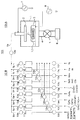
図1は、本発明の実施の形態に係る半導体装置の製造方法に用いられる平行平板型のプラズマ成膜装置101の構成を示す側面図である。
(First Embodiment)
FIG. 1 is a side view showing a configuration of a parallel plate type plasma
このプラズマ成膜装置101は、プラズマガスにより被成膜基板21上に絶縁膜を形成する場所である成膜部101Aと、成膜ガスを構成する複数のガスの供給源を有する成膜ガス供給部101Bとから構成されている。
The plasma
成膜部101Aは、図1に示すように、減圧可能なチャンバ1を備え、チャンバ1は排気配管4を通して排気装置6と接続されている。排気配管4の途中にはチャンバ1と排気装置6の間の導通/非導通を制御する開閉バルブ5が設けられている。チャンバ1にはチャンバ1内の圧力を監視する不図示の真空計などの圧力計測手段が設けられている。
As shown in FIG. 1, the
チャンバ1内には対向する一対の上部電極(第2の電極)2と下部電極(第1の電極)3とが備えられ、上部電極2に周波数13.56MHzの高周波電力を供給する高周波電力供給電源(RF電源)7が接続され、下部電極3に周波数380kHzの低周波電力を供給する低周波電力供給電源8が接続されている。これらの電源7、8から上部電極2及び下部電極3に電力を供給して、成膜ガスをプラズマ化する。上部電極2、下部電極3及び電源7、8が成膜ガスをプラズマ化するプラズマ生成手段を構成する。
The
上部電極2は成膜ガスの分散具を兼ねている。上部電極2には複数の貫通孔が形成され、下部電極3との対向面における貫通孔の開口部が成膜ガスの放出口(導入口)となる。この成膜ガス等の放出口は成膜ガス供給部101Bと配管9aで接続されている。また、場合により、上部電極2には図示しないヒータが備えられることもある。成膜中に上部電極2を温度凡そ100乃至200℃程度に加熱することにより、成膜ガス等の反応生成物からなるパーティクルが上部電極2に付着するのを防止するためである。
The
下部電極3は被成膜基板21の保持台を兼ね、また、保持台上の被成膜基板21を加熱するヒータ12を備えている。
The lower electrode 3 also serves as a holder for the
成膜ガス供給部101Bには、シロキサン結合を有するアルキル化合物の供給源と、メチルシラン(SiHn(CH3)4-n :n=0,1,2,3)の供給源と、アセチレン(C2H2)、シクロヘキサン(C6H12)、メチルシクロヘキサン(CH3C6H11)のうち何れか一の供給源と、ベンゼン(C6H6)の供給源と、メチルアルコール(CH3OH)又はエチルアルコール(C2H5OH)のうち何れか一の供給源と、酸素含有ガスの供給源と、アンモニア(NH3)の供給源と、希釈ガスの供給源と、窒素(N2)の供給源とが設けられている。
The film forming
これらのガスは適宜分岐配管9b乃至9j及びこれらすべての分岐配管9b乃至9jが接続された配管9aを通して成膜部101Aのチャンバ1内に供給される。分岐配管9b乃至9jの途中に流量調整手段11a乃至11iや、分岐配管9b乃至9jの導通/非導通を制御する開閉手段10b乃至10n、10p乃至tが設置され、配管9aの途中に配管9aの閉鎖/導通を行う開閉手段10aが設置されている。
These gases are appropriately supplied into the
また、N2ガスを流通させて分岐配管9b乃至9e、9g、9h内の残留ガスをパージするため、N2ガスの供給源と接続された分岐配管9jとその他の分岐配管9b乃至9e、9g、9hの間の導通/非導通を制御する開閉手段10u乃至10zが設置されている。なお、N2ガスは分岐配管9b乃至9e、9g、9h内のほかに、配管9a内及びチャンバ1内の残留ガスをパージする。他に、希釈ガスとして用いることもある。
Further, in order to circulate the N 2 gas and purge the residual gas in the branch pipes 9b to 9e, 9g and 9h, the branch pipe 9j connected to the N 2 gas supply source and the other branch pipes 9b to 9e and 9g , 9h are provided with opening / closing means 10u to 10z for controlling conduction / non-conduction between them. The N 2 gas purges residual gases in the
以上のような成膜装置101によれば、シロキサンの供給源と、酸素含有ガスの供給源と、不活性ガスの供給源とを備え、さらに成膜ガスをプラズマ化するプラズマ生成手段2、3、7、8を備えている。
According to the
これにより、下記の実施の形態に示すように、プラズマCVD法により低い誘電率を有する絶縁膜であって、かつ銅膜を主とする配線と密着強度の高い絶縁膜を形成することができる。 Accordingly, as described in the following embodiment, an insulating film having a low dielectric constant and high adhesion strength to a wiring mainly including a copper film can be formed by a plasma CVD method.
そして、プラズマ生成手段として、例えば平行平板型の上部電極2及び下部電極3によりプラズマを生成する手段があり、上部電極2及び下部電極3にそれぞれ高低2つの周波数の電力を供給する電源7、8が接続されている。従って、これら高低2つの周波数の電力をそれぞれ各電極2、3に印加してプラズマを生成することができる。特に、このようにして生成した絶縁膜は緻密であり、かつCH3を含むため、低誘電率を有する。
As plasma generation means, there is a means for generating plasma using, for example, a parallel plate type
上部電極2及び下部電極3への電力印加の好ましい組み合わせは、以下の通りである。
Preferred combinations of applying power to the
第1に、低圧絶縁膜を形成する工程において、下部電極3に周波数100kHz以上、1MHz未満の低周波電力を印加するか、又は下部電極3に低周波電力を印加し、かつ上部電極2に1MHz以上の高周波電力を印加し、高圧絶縁膜を形成する工程において、上部電極2に高周波電力を印加する。
First, in the step of forming the low-voltage insulating film, low-frequency power having a frequency of 100 kHz or more and less than 1 MHz is applied to the lower electrode 3 or low-frequency power is applied to the
第2に、第1の高圧絶縁膜を形成する工程において、上部電極2に高周波電力を印加することに加えて、下部電極3に低周波電力を印加する。
Second, in the step of forming the first high-voltage insulating film, low-frequency power is applied to the lower electrode 3 in addition to applying high-frequency power to the
第3に、特に、バリア絶縁膜を含む絶縁膜におけるバリア絶縁膜を成膜するためにこの発明の製造方法を用い、低圧絶縁膜を形成する工程において、下部電極3に周波数100kHz以上、1MHz未満の低周波電力を印加し、高圧絶縁膜を形成する工程において、下部電極3に低周波電力を印加する。このとき、上部電極2に高周波電力を加えてもよい。
Third, in particular, in the step of forming the low-voltage insulating film by using the manufacturing method of the present invention for forming the barrier insulating film in the insulating film including the barrier insulating film, the frequency of the lower electrode 3 is not less than 100 kHz and less than 1 MHz. Is applied to the lower electrode 3 in the step of forming the high-voltage insulating film. At this time, high frequency power may be applied to the
次に、本発明が適用される成膜ガスであるシロキサン結合を有するアルキル化合物、メチルシラン、ハイドロカーボン、酸素含有ガス、及び希釈ガスについては、代表例として以下に示すものを用いることができる。 Next, as a film forming gas to which the present invention is applied, the following compounds can be used as representative examples of the alkyl compound having a siloxane bond, methylsilane, hydrocarbon, oxygen-containing gas, and diluent gas.
(i)シロキサン結合を有するアルキル化合物
ヘキサメチルジシロキサン(HMDSO:(CH3)3Si-O-Si(CH3)3)
オクタメチルシクロテトラシロキサン(OMCTS:((CH3)2)4Si4O4)、
(I) alkyl compound hexamethyldisiloxane having a siloxane bond (HMDSO: (CH 3) 3 Si-O-Si (CH 3) 3)
Octamethylcyclotetrasiloxane (OMCTS: ((CH 3) 2) 4 Si 4 O 4),
テトラメチルシクロテトラシロキサン(TMCTS:(CH3H)4Si4O4) Tetramethylcyclotetrasiloxane (TMCTS: (CH 3 H) 4 Si 4 O 4 )
(ii)メチルシラン(SiHn(CH3)4-n:n=0,1,2,3)
モノメチルシラン(SiH3(CH3))
ジメチルシラン(SiH2(CH3)2)
トリメチルシラン(SiH(CH3)3)
テトラメチルシラン(Si(CH3)4)
(iii)ハイドロカーボン(CxHy)
アセチレン(C2H2)
メチルシクロヘキサン(CH3C6H11)
シクロヘキサン(C6H12)
ベンゼン(C6H6)
(iv)酸素含有ガス
一酸化窒素(N2O)
水(H2O)
炭酸ガス(CO2)
(v)希釈ガス
ヘリウム(He)
アルゴン(Ar)
窒素(N2)
次に、本願発明者の行なった実験について説明する。
(Ii) Methylsilane (SiH n (CH 3 ) 4-n : n = 0, 1, 2, 3)
Monomethylsilane (SiH 3 (CH 3 ))
Dimethylsilane (SiH 2 (CH 3 ) 2 )
Trimethylsilane (SiH (CH 3) 3)
Tetramethylsilane (Si (CH 3) 4)
(Iii) hydrocarbon (C x H y)
Acetylene (C 2 H 2 )
Methylcyclohexane (CH 3 C 6 H 11)
Cyclohexane (C 6 H 12 )
Benzene (C 6 H 6 )
(Iv) Oxygen-containing gas Nitric oxide (N 2 O)
Water (H 2 O)
Carbon dioxide (CO 2 )
(V) Diluent gas helium (He)
Argon (Ar)
Nitrogen (N 2)
Next, an experiment performed by the present inventors will be described.
以下の成膜条件により、プラズマ励起CVD法(PECVD法)によりSi基板上にシリコン酸化膜を図7の成膜手順により成膜した。シロキサン結合を有するアルキル化合物としてHMDSOを用い、酸素含有ガスとしてN2Oを用い、希釈ガスとしてHeを用いた。なお、成膜においては、図7に示すように、ガス導入から成膜開始(プラズマ励起)までのチャンバ内のガスの置換に必要な時間(安定化期間)を1分30秒間とり、上部電極2への反応生成物の付着を防止するため上部電極2を100℃で加熱している。
Under the following film forming conditions, a silicon oxide film was formed on a Si substrate by a plasma excitation CVD method (PECVD method) according to the film forming procedure of FIG. HMDSO was used as an alkyl compound having a siloxane bond, N 2 O was used as an oxygen-containing gas, and He was used as a diluent gas. In the film formation, as shown in FIG. 7, the time required for replacing the gas in the chamber from the gas introduction to the start of film formation (plasma excitation) (stabilization period) is 1
成膜条件
成膜ガス
HMDSO流量:50 SCCM
N2O流量 :200 SCCM
He流量 :400 SCCM
ガス圧力(パラメータ):0.75乃至1.75 Torr
プラズマ励起条件
下部電極(第1の電極)
低周波電力(周波数380kHz)(パラメータ):0乃至100W
上部電極(第2の電極)
高周波電力(周波数13.56MHz):250W
基板加熱条件:375℃
(a)成膜ガスのガス圧力と剥離強度の関係
図2は、成膜ガスのガス圧力とSi基板上に形成した成膜の剥離強度の関係を示す図である。縦軸は線形目盛りで表した成膜の剥離強度(g重)を示し、横軸は線形目盛りで表した成膜ガスのガス圧力(Torr)を示す。
Deposition conditions Deposition gas HMDSO flow rate: 50 SCCM
N2O flow rate: 200 SCCM
He flow rate: 400 SCCM
Gas pressure (parameter): 0.75 to 1.75 Torr
Plasma excitation condition Lower electrode (first electrode)
Low frequency power (frequency 380 kHz) (parameter): 0 to 100 W
Upper electrode (second electrode)
High frequency power (frequency 13.56 MHz): 250 W
Substrate heating condition: 375 ° C
(A) Relationship Between Gas Pressure of Film-Forming Gas and Peeling Strength FIG. 2 is a diagram showing a relationship between gas pressure of the film-forming gas and peeling strength of a film formed on a Si substrate. The vertical axis indicates the peel strength (g weight) of the film formed on a linear scale, and the horizontal axis indicates the gas pressure (Torr) of the film forming gas on a linear scale.
調査用絶縁膜は、上記成膜条件のパラメータのうち、下部電極3への低周波電力の印加を行なわず、成膜ガスのガス圧力0.9、1.5Torrの2条件でSi基板上に成膜した。また、剥離強度は島津製作所製の測定器(シマズ走査型スクラッチテスタ SST101)を用いて測定した。 The insulating film for investigation is formed on the Si substrate under the two conditions of the gas pressure of the film forming gas of 0.9 and 1.5 Torr without applying the low frequency power to the lower electrode 3 among the parameters of the above film forming conditions. A film was formed. The peel strength was measured using a measuring device (Shimadzu scanning scratch tester SST101) manufactured by Shimadzu Corporation.
図2によれば、ガス圧力1.5Torrのとき、5乃至6程度であった剥離強度がガス圧力0.9Torrのとき、15乃至16と3倍程度に大幅に改善された。 According to FIG. 2, when the gas pressure was 1.5 Torr, the peel strength was about 5 to 6, and when the gas pressure was 0.9 Torr, the peel strength was greatly improved to about 15 to 16, which is about three times.
なお、上記調査では、被成膜基板としてSi基板を用い、Si基板に対する剥離強度を調査しているが、銅基板に対する剥離強度も同じ傾向があると考えられる。 Note that, in the above investigation, the peel strength with respect to the Si substrate is examined using the Si substrate as the substrate on which the film is to be formed, but the peel strength with respect to the copper substrate is considered to have the same tendency.
(b)被成膜基板バイアスの低周波電力と剥離強度の関係
図3は、プラズマ励起条件の下部電極3に印加した低周波電力とSi基板上に形成した成膜の剥離強度の関係を示す図である。縦軸は線形目盛りで表した成膜の剥離強度(g重)を示し、横軸は線形目盛りで表した低周波電力(W)を示す。
(B) Relationship between Low-Frequency Power of Film Deposition Substrate Bias and Peeling Strength FIG. 3 shows the relationship between low-frequency power applied to the lower electrode 3 under plasma excitation conditions and peeling strength of a film formed on a Si substrate. FIG. The vertical axis shows the peel strength (g weight) of the film formed on a linear scale, and the horizontal axis shows the low frequency power (W) on a linear scale.
調査用絶縁膜は、上記成膜条件のパラメータのうち、成膜ガスのガス圧力1.5Torrとし、低周波電力0,10,30,50,75,100Wの6条件で成膜した。測定装置は(a)と同じものを用いた。 The inspection insulating film was formed under the following conditions: the gas pressure of the film forming gas was 1.5 Torr, and the low frequency power was 0, 10, 30, 50, 75, and 100 W. The same measuring device as in (a) was used.
図3によれば、低周波電力が30W以下で、0Wのときの凡そ6から、30Wのときの凡そ3.3のように、電力の増加とともに剥離強度が低下した。低周波電力が30Wよりも大きくなると、剥離強度はあまり低下せず、3前後に落ち着いた。 According to FIG. 3, when the low-frequency power is 30 W or less, the peel strength decreases as the power increases, from about 6 at 0 W to about 3.3 at 30 W. When the low-frequency power was larger than 30 W, the peel strength did not decrease so much and settled to around 3.
(c)成膜ガスのガス圧力と膜硬度の関係
図4は、成膜ガスのガス圧力とSi基板上に形成した成膜の膜硬度及びヤング率(Young's Modulus)の関係を示す図である。縦軸の左側は線形目盛りで表した成膜の膜硬度を示し、同じく右側は線形目盛りで表した成膜のヤング率(GP)を示し、横軸は線形目盛りで表した成膜ガスのガス圧力(Torr)を示す。
(C) Relationship Between Gas Pressure of Film Forming Gas and Film Hardness FIG. 4 is a diagram showing a relationship between the gas pressure of the film forming gas and the film hardness and Young's Modulus of the film formed on the Si substrate. . The left side of the vertical axis shows the film hardness of the film formed on a linear scale, the right side shows the Young's modulus (GP) of the film formed on a linear scale, and the horizontal axis shows the gas of the film forming gas expressed on a linear scale. Indicates pressure (Torr).
調査用絶縁膜は、上記成膜条件のパラメータのうち、下部電極3への低周波電力の印加を行なわず、成膜ガスのガス圧力0.7,0.9,1.1,1.3,1.5,1.7Torrの6条件で作成した。膜硬度、ヤング率(Young's Modulus)は、島津製作所製の測定器(シマズダイナミック超微小硬度計 DUH−W201S)を用いて測定した。 In the inspection insulating film, of the parameters of the film forming conditions, the low-frequency power is not applied to the lower electrode 3 and the gas pressures of the film forming gas are 0.7, 0.9, 1.1, and 1.3. , 1.5, 1.7 Torr. The film hardness and Young's Modulus were measured using a measuring instrument (Shimazu Dynamic Ultra-Micro Hardness Tester DUH-W201S) manufactured by Shimadzu Corporation.
図4によれば、ガス圧力0.7Torrから1.3Torrまで、ガス圧力の増加とともに、膜硬度は低下する。ガス圧力0.7Torrのとき230程度で、ガス圧力1.3Torrのとき70乃至80程度であった。ガス圧力がこれより大きくなると膜硬度は50前後に落ち着き、あまり変化しなくなった。 According to FIG. 4, the film hardness decreases from 0.7 Torr to 1.3 Torr as the gas pressure increases. The gas pressure was about 230 when the gas pressure was 0.7 Torr, and was about 70 to 80 when the gas pressure was 1.3 Torr. When the gas pressure was higher than this, the film hardness settled to around 50 and did not change much.
ヤング率(Young's Modulus)も膜硬度とほぼ同じ傾向を示した。ガス圧力0.7Torrのとき40GP程度で、ガス圧力1.3Torrのとき10程度であった。ガス圧力がこれより大きくなるとヤング率は10GP前後に落ち着いた。 Young's Modulus showed almost the same tendency as the film hardness. The gas pressure was about 40 GP when the gas pressure was 0.7 Torr, and about 10 when the gas pressure was 1.3 Torr. When the gas pressure became higher than this, the Young's modulus settled around 10 GP.
(d)被成膜基板バイアスの低周波電力と膜硬度の関係
図5は、被成膜基板への直流バイアス電圧を形成する下部電極3に印加した低周波電力とSi基板上に形成した成膜の膜硬度及びヤング率の関係を示す図である。縦軸の左側は線形目盛りで表した膜硬度を示し、同じく右側は線形目盛りで表した成膜のヤング率(GP)を示し、横軸は線形目盛りで表した低周波電力(W)を示す。
(D) Relationship between Low-Frequency Power of Film Deposition Substrate Bias and Film Hardness FIG. 5 shows the low frequency power applied to the lower electrode 3 for forming a DC bias voltage for the film deposition substrate and the film formed on the Si substrate. FIG. 3 is a diagram illustrating a relationship between a film hardness and a Young's modulus of the film. The left side of the vertical axis shows the film hardness expressed on a linear scale, the right side shows the Young's modulus (GP) of the film formation expressed on a linear scale, and the horizontal axis shows the low frequency power (W) expressed on a linear scale. .
調査用絶縁膜は、上記成膜条件のパラメータのうち、成膜ガスのガス圧力1.5Torrとし、低周波電力0,10,30,50,75,100Wの6条件で成膜した。測定装置は(c)と同じものを用いた。 The inspection insulating film was formed under the following conditions: the gas pressure of the film forming gas was 1.5 Torr, and the low frequency power was 0, 10, 30, 50, 75, and 100 W. The same measuring device as in (c) was used.
図5によれば、低周波電力0から75Wまでは、低周波電力の増加とともに、膜硬度も高くなっていく。低周波電力がそれ以上増加すると、膜硬度は漸増する。膜硬度は、低周波電力を印加しないとき約50、75Wのとき約290、100Wのとき約300であった。 According to FIG. 5, from 0 to 75 W of low frequency power, the film hardness increases as the low frequency power increases. As the low frequency power further increases, the film hardness gradually increases. The film hardness was about 50, 75 W when no low-frequency power was applied, about 290 at 100 W, and about 300 at 100 W.
ヤング率も膜硬度と同様な傾向を示し、低周波電力を印加しないとき約8、75Wのとき約47、100Wのとき約50であった。 The Young's modulus also showed a tendency similar to the film hardness, and was about 8, 75 W when no low-frequency power was applied, and about 50 when 100 W was applied.
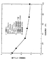
(e)被成膜基板バイアスの低周波電力と成膜の比誘電率の関係
図6は、被成膜基板への直流バイアス電圧を形成する下部電極3に印加した低周波電力とSi基板上に形成した成膜の比誘電率の関係を示す図である。縦軸は線形目盛りで表した成膜の比誘電率を示し、横軸は線形目盛りで表した低周波電力(W)を示す。
(E) Relationship between low-frequency power of substrate bias for film formation and relative dielectric constant of film formation FIG. 6 shows the relationship between low-frequency power applied to lower electrode 3 for forming a DC bias voltage for film formation substrate and Si substrate. FIG. 4 is a diagram showing a relationship between relative dielectric constants of a film formed in FIG. The vertical axis shows the relative dielectric constant of the film formed on a linear scale, and the horizontal axis shows the low frequency power (W) on a linear scale.
調査用絶縁膜は、上記成膜条件のパラメータのうち、成膜ガスのガス圧力0.9,1.2,1.5Torrの3条件で、かつ低周波電力0,10,20,50,75,100Wの6条件で成膜した。比誘電率は直流バイアスに周波数1MHzの信号を重畳したC−V測定法により測定した。 The insulating film for inspection is formed under the three conditions of the gas pressure of the film forming gas of 0.9, 1.2, and 1.5 Torr and the low frequency power of 0, 10, 20, 50, 75 among the parameters of the above film forming conditions. , 100W. The relative permittivity was measured by a CV measurement method in which a signal having a frequency of 1 MHz was superimposed on a DC bias.
なお、図中、ガス圧1.5Torrの場合、調査点付近の数字は膜硬度を示す。 In the figure, when the gas pressure is 1.5 Torr, the numbers near the inspection points indicate the film hardness.
図6によれば、ガス圧力0.9Torrの場合、低周波電力0から20Wまでは比誘電率は2.9から4.3くらいまで急激に増加し、それ以上の低周波電力では漸減している。ガス圧力1.2Torrの場合、低周波電力0から20Wまでは比誘電率は2.7から3.9くらいまで急激に増加し、それ以上は漸増し、100Wで4.8程度になっている。ガス圧力1.5Torrの場合も、ガス圧力1.2Torrの場合と同じように、低周波電力0から20Wまでは比誘電率は2.7から3.6くらいまで急激に増加し、それ以上の低周波電力では漸増し、100Wで4.1程度になっている。 According to FIG. 6, when the gas pressure is 0.9 Torr, the relative dielectric constant sharply increases from 2.9 to 4.3 at a low frequency power of 0 to 20 W, and gradually decreases at a low frequency power of more than 2.9. I have. In the case of a gas pressure of 1.2 Torr, the relative dielectric constant sharply increases from 2.7 to about 3.9 from 0 to 20 W of low frequency power, and gradually increases from that point to about 4.8 at 100 W. . In the case of a gas pressure of 1.5 Torr, the relative dielectric constant sharply increases from 2.7 to 3.6 from 0 to 20 W of low-frequency power, as in the case of a gas pressure of 1.2 Torr. It gradually increases at low frequency power and reaches about 4.1 at 100 W.
以上のように、第1の実施の形態によれば、成膜ガス圧力に関しては、低い方が、剥離強度が大きいが、比誘電率は高くなることが分かった。特に、1Torr以下で剥離強度が大きく、1Torr以上で比誘電率が小さい。また、低周波電力に関しては、小さい方が、剥離強度が大きく、かつ比誘電率が低くなることが分かった。 As described above, according to the first embodiment, it was found that the lower the deposition gas pressure, the higher the peel strength but the higher the relative dielectric constant. In particular, the peel strength is large at 1 Torr or less, and the relative dielectric constant is small at 1 Torr or more. Further, it was found that the smaller the low frequency power, the larger the peel strength and the lower the relative dielectric constant.
従って、低誘電率を有する絶縁膜を銅膜を主とする配線の間の層間絶縁膜として形成する場合、成膜初期は、比誘電率を多少犠牲にして、ガス圧を、例えば1Torr未満と低くし、かつ低周波電力を小さくして剥離強度を大きくし、残りの成膜をガス圧を、例えば1Torr以上と高くして行い、膜全体の比誘電率を低くすることが望ましい。 Therefore, when an insulating film having a low dielectric constant is formed as an interlayer insulating film between wirings mainly composed of a copper film, the gas pressure is reduced to, for example, less than 1 Torr at the initial stage of film formation while sacrificing the relative dielectric constant somewhat. It is desirable that the peeling strength be increased by lowering the low-frequency power and the low frequency power be increased, and the remaining film be formed by increasing the gas pressure to, for example, 1 Torr or more, thereby lowering the relative dielectric constant of the entire film.
また、銅膜を主とする配線と接するバリア絶縁膜として形成する場合は、ガス圧力の調整は低圧絶縁膜と高圧絶縁膜とで層間絶縁膜と同様に行なうが、プラズマ励起のための電力の周波数の調整は行なわず、低圧絶縁膜も高圧絶縁膜もともに低周波数とする。即ち、成膜初期は、比誘電率を多少犠牲にして、ガス圧を、例えば1Torr未満と低くし、かつ低周波電力を小さくして剥離強度を大きくし、残りの成膜をガス圧を、例えば1Torr以上と高くして行い、膜全体の比誘電率を低くすることが望ましい。 In the case of forming a barrier insulating film in contact with a wiring mainly composed of a copper film, the gas pressure is adjusted in the same manner as the interlayer insulating film in the low-voltage insulating film and the high-pressure insulating film, but the power for plasma excitation is reduced. The frequency is not adjusted, and both the low-voltage insulating film and the high-voltage insulating film have a low frequency. That is, in the initial stage of film formation, the gas pressure is reduced to, for example, less than 1 Torr, the peel strength is increased by reducing the low-frequency power, and the gas pressure is reduced for the remaining film formation, at the expense of the relative dielectric constant to some extent. For example, it is desirable to increase the relative dielectric constant of the entire film to 1 Torr or more to lower the relative dielectric constant.
なお、成膜初期においてガス圧を1Torr未満が好ましいが、ガス圧が0.1Torrより小さいと、成膜レートが遅く実用的でない。また、残りの成膜においてガス圧を1Torr以上が好ましいが、放電の関係で最大10Torrとすることが実用的である。 Although the gas pressure is preferably less than 1 Torr at the beginning of film formation, if the gas pressure is less than 0.1 Torr, the film formation rate is too slow to be practical. In the remaining film formation, the gas pressure is preferably 1 Torr or more, but it is practical to set the gas pressure to 10 Torr at the maximum in terms of discharge.
(第2の実施の形態)
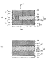
次に、図8(a)、(b)を参照して、本発明の第2の実施の形態に係る半導体装置及びその製造方法を説明する。
(Second embodiment)
Next, a semiconductor device and a method of manufacturing the same according to a second embodiment of the present invention will be described with reference to FIGS.
図8(a)は、本発明の第2の実施の形態に係る半導体装置の製造方法により作成された半導体装置を示す断面図である。同図(b)は同図(a)のI−I線断面図である。下部配線33が埋め込まれた下部配線埋込絶縁膜32と上部配線37が埋め込まれた上部配線埋込絶縁膜35との間に挟まれた配線層間絶縁膜34の成膜ガスとしてHMDSO+N2O+Heを用いている。
FIG. 8A is a cross-sectional view showing a semiconductor device manufactured by the method for manufacturing a semiconductor device according to the second embodiment of the present invention. FIG. 2B is a cross-sectional view taken along the line II of FIG. HMDSO + N 2 O + He is used as a film forming gas for the wiring
まず、図8(a)に示すように、基板(被成膜基板)31上に、膜厚約1μmのSiO2膜又はSiOCH膜からなる配線埋込絶縁膜32を形成する。なお、SiOCH膜は膜中にSi,O,C,Hを含む絶縁膜である。
First, as shown in FIG. 8A, a wiring buried insulating
続いて、配線埋込絶縁膜32をエッチングして配線溝を形成した後、配線溝の内面に銅拡散防止膜としてTaN膜33aを形成する。次いで、TaN膜33a表面に図示しない銅シード層をスパッタ法により形成した後、メッキ法により銅膜を埋め込む。CMP法(Chemical Mechanical Polishing 法)により、配線溝から突出した銅膜及びTaN膜33aを研磨して表面を平坦化する。これにより、銅膜を主とする配線33b及びTaN膜33aからなる下部配線が形成される。
Subsequently, after the wiring buried insulating
次に、HMDSO+N2O+Heを用いたプラズマCVD法により膜厚数10nmのPE-CVD SiOCH膜からなる配線層間絶縁膜34を形成する。以下にその詳細を説明する。
Next, a wiring
即ち、配線層間絶縁膜34を形成するには、まず、被成膜基板21を成膜装置101のチャンバ1内に導入し、基板保持具3に保持する。続いて、被成膜基板21を加熱し、温度375℃に保持する。HMDSOを流量50sccmで、N2Oガスを流量200sccmで、Heガスを流量400sccmで、図1に示すプラズマ成膜装置101のチャンバ1内に導入し、圧力を0.7Torrに保持する。次いで、下部電極3に周波数380kHzの低周波電力100乃至150Wを印加し、上部電極2に周波数13.56MHzの高周波電力250W(0.3W/cm2に相当)を印加する。
That is, in order to form the wiring
これにより、HMDSOとN2OとHeがプラズマ化する。この状態を40秒間保持して、膜厚凡そ100nmのPE-CVD SiOC膜からなる低圧絶縁膜34aを形成する。なお、SiOC膜は膜中にSi,O,Cを含む絶縁膜である。
Thereby, HMDSO, N 2 O, and He are turned into plasma. While maintaining this state for 40 seconds, a low-
引き続き、同じ反応ガスの組み合わせを用い、かつ同じ流量を保持し、ガス圧力を1.5Torrに調整し、同じプラズマ励起条件で成膜する。膜厚約500nmのPE-CVD SiOCH膜からなる高圧絶縁膜34bが形成される。
Subsequently, using the same combination of reaction gases, maintaining the same flow rate, adjusting the gas pressure to 1.5 Torr, and forming a film under the same plasma excitation conditions. A high-
以上により、低圧絶縁膜34aと高圧絶縁膜34bからなる配線層間絶縁膜34が形成される。
As described above, the wiring
次いで、配線層間絶縁膜34上にSiO2膜又はSiOCH膜32を形成したときと同じ方法により膜厚約1μmのSiO2膜又はSiOCH膜からなる配線埋込絶縁膜35を形成する。
Next, a wiring buried insulating
次に、よく知られたデュアルダマシン法により銅膜を主とする接続導体36と上部配線37を形成する。なお、図中、符号36a、37aはTaN膜であり、符号36b、37bは銅膜である。
Next, a
次に、全面にバリア絶縁膜38を形成する。これにより、半導体装置が完成する。
Next, a
以上のように、この第2の実施の形態によれば、下部配線33が埋め込まれた下部配線埋込絶縁膜32と上部配線37が埋め込まれた上部配線埋込絶縁膜35の間に配線層間絶縁膜34を挟んでなる半導体装置の製造方法において、成膜ガスのガス圧力を1Torr未満で初期成膜し、同じく1Torr以上で残りをプラズマ励起CVD法により配線層間絶縁膜34を形成している。
As described above, according to the second embodiment, the wiring interlayer is formed between the lower wiring buried insulating
これにより、銅膜33bに対して密着性が高く、かつ全体として3以下の低比誘電率を有する層間絶縁膜34を形成することができる。
Thereby, the
以上、第2の実施の形態によりこの発明を詳細に説明したが、この発明の範囲は上記実施の形態に具体的に示した例に限られるものではなく、この発明の要旨を逸脱しない範囲の上記実施の形態の変更はこの発明の範囲に含まれる。 As described above, the present invention has been described in detail with reference to the second embodiment. However, the scope of the present invention is not limited to the example specifically shown in the above embodiment, and the scope of the present invention does not depart from the gist of the present invention. Modifications of the above embodiment are included in the scope of the present invention.
第2の実施の形態で用いたHMDSOの代わりに、第1の実施の形態で記載した他のシロキサン結合を有するアルキル化合物の代わりに、メチルシラン(SiHn(CH3)4-n:n=0,1,2,3)を用いることができる。メチルシランの種類は第1の実施の形態に示したので、ここでは省略する。 Instead of the HMDSO used in the second embodiment, the other alkyl compound having a siloxane bond described in the first embodiment is replaced with methylsilane (SiH n (CH 3 ) 4-n : n = 0). , 1, 2, 3) can be used. The type of methylsilane has been described in the first embodiment, and will not be described here.
また、成膜ガスは、アセチレン(C2H2)、メチルシクロヘキサン(CH3C6H11)又はシクロヘキサン(C6H12)のうち何れか一を含むものでもよい。膜の多孔性が増加し、誘電率を更に低下させることができる。 Further, the deposition gas may contain any one of acetylene (C 2 H 2 ), methylcyclohexane (CH 3 C 6 H 11 ), and cyclohexane (C 6 H 12 ). The porosity of the membrane increases and the dielectric constant can be further reduced.
また、成膜ガスは、ベンゼン(C6H6)を含むものでもよい。 Further, the deposition gas may contain benzene (C 6 H 6 ).
また、成膜ガスは、メチルアルコール(CH3OH)又はエチルアルコール(C2H5OH)を含むものでもよい。 Further, the deposition gas may contain methyl alcohol (CH 3 OH) or ethyl alcohol (C 2 H 5 OH).
また、成膜ガスは、ヘリウム(He)の代わりに、アルゴン(Ar)又は窒素(N2)のうち何れか一を含む不活性ガスを加えてもよい。 As the deposition gas, an inert gas containing any one of argon (Ar) and nitrogen (N 2 ) may be added instead of helium (He).
また、バリア絶縁膜38を下記第3の実施の形態のバリア絶縁膜39aと同じ成膜方法により成膜してもよい。
Further, the
(第3の実施の形態)
図9(a)は、第3の実施の形態である半導体装置の製造方法について示す断面図である。図9(b)は、図9(a)のII-II線に沿う断面図である。
(Third embodiment)
FIG. 9A is a cross-sectional view illustrating a method for manufacturing the semiconductor device according to the third embodiment. FIG. 9B is a cross-sectional view taken along the line II-II of FIG.
図8(a)、(b)と異なるところは、バリア絶縁膜39a、39cを含む層間絶縁膜39のうち、銅膜を主とする配線と接するバリア絶縁膜39aにこの発明の製造方法を適用している点である。
8A and 8B is that the manufacturing method of the present invention is applied to a
以下に、第3の実施の形態である半導体装置の製造方法について説明する。なお、図9(a)、(b)中、図8(a)、(b)中の符号と同じ符号で示すものは図8(a)、(b)中のものと同じものを示すので、説明を省略する。 Hereinafter, a method for manufacturing a semiconductor device according to the third embodiment will be described. 9A and 9B, the same reference numerals as those in FIGS. 8A and 8B indicate the same components as those in FIGS. 8A and 8B. The description is omitted.
まず、第2の実施の形態と同様な方法で、基板(被成膜基板)31上に、膜厚約1μmのSiO2膜又はSiOCH膜からなる配線埋込絶縁膜32と、配線埋込絶縁膜32の配線溝に銅膜を主とする配線33b及びTaN膜33aからなる下部配線とを形成する。
First, in the same manner as in the second embodiment, a wiring buried insulating
次いで、配線層間絶縁膜39のうち銅膜と接するバリア絶縁膜39aをHMDSO+N2O+NH3の成膜ガスを用いたプラズマCVD法により形成する。以下にその詳細を説明する。
Next, a
即ち、バリア絶縁膜39aを形成するには、まず、被成膜基板21を成膜装置101のチャンバ1内に導入し、基板保持具3に保持する。続いて、被成膜基板21を加熱し、温度375℃に保持する。HMDSOを流量凡そ50sccmで、N2Oを流量凡そ200sccmで、NH3ガスを流量凡そ50sccmで、図1に示すプラズマ成膜装置101のチャンバ1内に導入し、圧力を0.7Torrに保持する。なお、上記成膜ガスにHeガスを加えてもよく、この場合、流量約400sccmとするとよい。
That is, in order to form the
次いで、下部電極3に周波数380kHzの低周波電力約150Wを印加する。上部電極2には高周波電力を印加しない。
Next, a low-frequency power of about 150 W having a frequency of 380 kHz is applied to the lower electrode 3. No high-frequency power is applied to the
これにより、HMDSOとN2OとNH3とがプラズマ化する。この状態を5秒間保持して、膜厚10nmのPE-CVD SiO2膜からなる低圧絶縁膜39aaを形成する。 As a result, HMDSO, N 2 O, and NH 3 are turned into plasma. While maintaining this state for 5 seconds, a low-voltage insulating film 39aa made of a 10-nm-thick PE-CVD SiO 2 film is formed.
引き続き、同じ反応ガスの組み合わせを用い、かつ同じ流量を保持し、ガス圧力を1.5Torrに調整し、同じプラズマ励起条件で成膜する。膜厚約90nmのPE-CVDSiOCN膜からなる高圧絶縁膜39abが形成される。 Subsequently, using the same combination of reaction gases, maintaining the same flow rate, adjusting the gas pressure to 1.5 Torr, and forming a film under the same plasma excitation conditions. A high-voltage insulating film 39ab made of a PE-CVD SiOCN film having a thickness of about 90 nm is formed.
以上により、低圧絶縁膜39aaと高圧絶縁膜39abからなるバリア絶縁膜39aが形成される。
As described above, the
次いで、通常の良く知られた低誘電率を有する絶縁膜の形成方法により、バリア絶縁膜39a上に低誘電率を有する主絶縁膜39b及びバリア絶縁膜39cを順次形成し、配線層間絶縁膜39を形成する。
Then, a main
次に、第2の実施の形態と同様にして、配線層間絶縁膜39上に配線埋込絶縁膜35と、接続導体36と、上部配線37と、バリア絶縁膜38とを順次形成する。
Next, as in the second embodiment, a wiring buried insulating
以上のように、この実施の形態によれば、銅膜を主とする配線上にバリア絶縁膜39a、39cを含む層間絶縁膜39を形成する際に、バリア絶縁膜39aを形成するため、初期成膜を低圧絶縁膜39aaとして形成し、残りを高圧絶縁膜39abとして形成し、低圧絶縁膜39aaも高圧絶縁膜39abもともに、低周波電力を用いて成膜ガスをプラズマ化している。
As described above, according to this embodiment, when forming the
低周波数の電力による成膜はもともと密着力は大きいが、成膜初期に低いガス圧の成膜ガスを用いて成膜することで、密着強度をさらに向上させることができる。 Although the adhesion is originally large when the film is formed by low-frequency power, the adhesion strength can be further improved by forming the film using a film-forming gas having a low gas pressure in the initial stage of the film formation.
以上、第3の実施の形態によりこの発明を詳細に説明したが、この発明の範囲は上記実施の形態に具体的に示した例に限られるものではなく、この発明の要旨を逸脱しない範囲の上記実施の形態の変更はこの発明の範囲に含まれる。 As described above, the present invention has been described in detail with reference to the third embodiment. However, the scope of the present invention is not limited to the example specifically shown in the above embodiment, and a range that does not depart from the gist of the present invention. Modifications of the above embodiment are included in the scope of the present invention.
第3の実施の形態で用いたHMDSOの代わりに、第1の実施の形態で記載した他のシロキサン結合を有するアルキル化合物でもよいし、メチルシラン(SiHn(CH3)4-n:n=0,1,2,3)を用いることができる。メチルシランの種類は第1の実施の形態に示したので、ここでは省略する。 Instead of the HMDSO used in the third embodiment, another alkyl compound having a siloxane bond described in the first embodiment may be used, or methylsilane (SiH n (CH 3 ) 4-n : n = 0) , 1, 2, 3) can be used. The type of methylsilane has been described in the first embodiment, and will not be described here.
また、成膜ガスは、アンモニア(NH3)又は窒素(N2)のうち何れか一を含む窒素含有ガスでもよい。 Further, the deposition gas may be a nitrogen-containing gas containing any one of ammonia (NH 3 ) and nitrogen (N 2 ).
また、成膜ガスは、ヘリウム(He)、アルゴン(Ar)又は窒素(N2)のうち何れか一を含む不活性ガスでもよい。これにより、成膜の所謂白濁を防止することができる。 Further, the deposition gas may be an inert gas containing any one of helium (He), argon (Ar), and nitrogen (N 2 ). As a result, so-called cloudiness of the film formation can be prevented.
また、層間絶縁膜39のうち、絶縁膜39bは第2の実施の形態の絶縁膜34bの成膜方法により形成してもよい。また、層間絶縁膜39のうち、バリア絶縁膜39cをバリア絶縁膜39aと同じ成膜方法により形成してもよい。但し、上部配線37と接する側を低圧絶縁膜とする。またバリア絶縁膜38をバリア絶縁膜39aと同じ成膜方法により形成してもよい。
The insulating
(第4の実施の形態)
上記実施の形態では、低誘電率を有する主絶縁膜の他に、主絶縁膜の下地のバリア絶縁膜を形成する方法に適用があるが、低誘電率を有する主絶縁膜を形成するだけの目的では、成膜中にガス圧力を変えなくてもよく、シロキサン結合を有するアルキル化合物と、アセチレン(C2H2)、メチルシクロヘキサン(CH3C6H11)又はシクロヘキサン(C6H12)のうち何れか一と、酸素含有ガスとを含む成膜ガス、又はシロキサン結合を有するアルキル化合物と、ベンゼン(C6H6)と、酸素含有ガスと、不活性ガスとを含む成膜ガスを用いて、同一のガス圧力を保持したまま、所望の主絶縁膜を成膜することができる。
(Fourth embodiment)
In the above embodiment, in addition to the main insulating film having a low dielectric constant, there is an application to a method of forming a barrier insulating film underlying the main insulating film. For the purpose, the gas pressure does not need to be changed during film formation, and an alkyl compound having a siloxane bond, acetylene (C 2 H 2 ), methylcyclohexane (CH 3 C 6 H 11 ) or cyclohexane (C 6 H 12 ) And a film-forming gas containing an oxygen-containing gas, or a film-forming gas containing an alkyl compound having a siloxane bond, benzene (C 6 H 6 ), an oxygen-containing gas, and an inert gas. In this manner, a desired main insulating film can be formed while maintaining the same gas pressure.
図9(a)、(b)を参照して、第4の実施の形態である半導体装置の製造方法について説明する。 A method for manufacturing a semiconductor device according to the fourth embodiment will be described with reference to FIGS.
第3の実施の形態と異なるところは、上下のバリア絶縁膜39a、39cと低誘電率を有する主絶縁膜39bを含む層間絶縁膜39のうち、バリア絶縁膜39a、39cにはさまれた、低誘電率を有する主絶縁膜39bにこの発明の製造方法を適用している点である。
The difference from the third embodiment is that the
以下に、第4の実施の形態である半導体装置の製造方法について説明する。主絶縁膜39bの成膜条件は以下の通りである。
Hereinafter, a method for manufacturing a semiconductor device according to the fourth embodiment will be described. The conditions for forming the main insulating
成膜ガス
HMDSO流量:50 sccm
N2O流量 :200 sccm
CH3C6H11流量:50 sccm
ガス圧力(パラメータ):0.9 Torr
プラズマ励起条件
下部電極(第1の電極)
低周波電力(周波数380kHz)(パラメータ):0W
上部電極(第2の電極)
高周波電力(周波数13.56MHz):250W
基板加熱条件:375℃
まず、第2の実施の形態と同様な方法で、基板(被成膜基板)31上に、膜厚約1μmのPE-CVD SiO2膜からなる配線埋込絶縁膜32と、配線埋込絶縁膜32の配線溝に銅膜を主とする配線33b及びTaN膜33aからなる下部配線とを形成する。
Deposition gas HMDSO flow rate: 50 sccm
N 2 O flow rate: 200 sccm
CH 3 C 6 H 11 flow rate: 50 sccm
Gas pressure (parameter): 0.9 Torr
Plasma excitation condition Lower electrode (first electrode)
Low frequency power (frequency 380 kHz) (parameter): 0 W
Upper electrode (second electrode)
High frequency power (frequency 13.56 MHz): 250 W
Substrate heating condition: 375 ° C
First, in the same manner as in the second embodiment, a wiring buried insulating
次いで、第3の実施の形態と同様に、HMDSO+N2O+NH3の成膜ガスを用いたプラズマCVD法により、配線層間絶縁膜39のうち銅膜と接するバリア絶縁膜39aを形成する。バリア絶縁膜39aは低圧絶縁膜39aaと高圧絶縁膜39abからなる。
Next, as in the third embodiment, a
次いで、上記成膜ガスを用いたプラズマCVD法により、バリア絶縁膜39a上に低誘電率を有する主絶縁膜39b及びバリア絶縁膜39cを順次形成し、配線層間絶縁膜39を形成する。
Next, a main
低誘電率を有する主絶縁膜39bを形成するため、まず、被成膜基板21を成膜装置101のチャンバ1内に導入し、基板保持具3に保持する。続いて、被成膜基板21を加熱し、温度375℃に保持する。HMDSOを流量50sccmで、N2Oガスを流量200sccmで、CH3C6H11を流量50sccmで、図1に示すプラズマ成膜装置101のチャンバ1内に導入し、圧力を0.9Torrに保持する。次いで、上部電極2に周波数13.56MHzの高周波電力250W(0.3W/cm2に相当)を印加する。このとき、下部電極3には低周波電力を印加しない。
In order to form the main insulating
これにより、HMDSOとN2OとCH3C6H11がプラズマ化する。この状態を40秒間保持して、膜厚凡そ500nmのPE-CVD SiO2膜からなる主絶縁膜39bが形成される。
Thus, HMDSO, N 2 O, and CH 3 C 6 H 11 are turned into plasma. While maintaining this state for 40 seconds, a main
次に、第2の実施の形態と同様にして、配線層間絶縁膜39上に配線埋込絶縁膜35と、接続導体36と、上部配線37と、バリア絶縁膜38とを順次形成する。
Next, as in the second embodiment, a wiring buried insulating
以上、第4の実施の形態によりこの発明を詳細に説明したが、この発明の範囲は上記実施の形態に具体的に示した例に限られるものではなく、この発明の要旨を逸脱しない範囲の上記実施の形態の変更はこの発明の範囲に含まれる。 As described above, the present invention has been described in detail with reference to the fourth embodiment. However, the scope of the present invention is not limited to the examples specifically shown in the above-described embodiment, and the scope of the present invention does not depart from the gist of the present invention. Modifications of the above embodiment are included in the scope of the present invention.
第4の実施の形態で用いたHMDSOの代わりに、第1の実施の形態で記載した他のシロキサン結合を有するアルキル化合物でもよいし、メチルシラン(SiHn(CH3)4-n:n=0,1,2,3)を用いることができる。メチルシランの種類は第1の実施の形態に示したので、ここでは省略する。 Instead of the HMDSO used in the fourth embodiment, the other alkyl compound having a siloxane bond described in the first embodiment may be used, or methylsilane (SiH n (CH 3 ) 4-n : n = 0) , 1, 2, 3) can be used. The type of methylsilane has been described in the first embodiment, and will not be described here.
また、成膜ガスは、ヘリウム(He)、アルゴン(Ar)又は窒素(N2)のうち何れか一を含む不活性ガスでもよい。この場合、アセチレン(C2H2)、メチルシクロヘキサン(CH3C6H11)又はシクロヘキサン(C6H12)のうち何れか一の代わりに、ベンゼン(C6H6)を用いてもよい。 Further, the deposition gas may be an inert gas containing any one of helium (He), argon (Ar), and nitrogen (N 2 ). In this case, benzene (C 6 H 6 ) may be used instead of acetylene (C 2 H 2 ), methylcyclohexane (CH 3 C 6 H 11 ) or cyclohexane (C 6 H 12 ). .
1 チャンバ
2 上部電極
3 下部電極
4 排気配管
5 バルブ
6 排気装置
7 高周波電力供給電源(RF電源)
8 低周波電力供給電源
9a 配管
9b〜9j 分岐配管
10a〜10n,10p〜10z 開閉手段
11a〜11i 流量調整手段
12 ヒータ
21 被成膜基板
31 基板
32 下部配線埋込絶縁膜(SiO2膜又はSiOCH膜)
33 下部配線
33a、36a、37a TaN膜
33b、36b、37b 銅膜
34、39 配線層間絶縁膜
34a、39aa 低圧絶縁膜
34b、39ab 高圧絶縁膜
35 上部配線埋込絶縁膜(SiO2膜又はSiOCH膜)
36 接続導体
37 上部配線
38、39a、39c バリア絶縁膜
39b 主絶縁膜
101A 成膜部
101B 成膜ガス供給部
DESCRIPTION OF
8 Low frequency power
33
36
Claims (10)
前記成膜ガスは、シロキサン結合を有するアルキル化合物と、ハイドロカーボン(CxHy)と、酸素含有ガスとを含むものであることを特徴とする半導体装置の製造方法。 In a method for manufacturing a semiconductor device, a film forming gas is turned into plasma and reacted to form an insulating film having a low dielectric constant on a substrate.
The method of manufacturing a semiconductor device, wherein the film forming gas contains an alkyl compound having a siloxane bond, a hydrocarbon (C x H y ), and an oxygen-containing gas.
Priority Applications (1)
| Application Number | Priority Date | Filing Date | Title |
|---|---|---|---|
| JP2004047027A JP2004200713A (en) | 2000-12-19 | 2004-02-23 | Semiconductor device and method of manufacturing the same |
Applications Claiming Priority (2)
| Application Number | Priority Date | Filing Date | Title |
|---|---|---|---|
| JP2000384825 | 2000-12-19 | ||
| JP2004047027A JP2004200713A (en) | 2000-12-19 | 2004-02-23 | Semiconductor device and method of manufacturing the same |
Related Parent Applications (1)
| Application Number | Title | Priority Date | Filing Date |
|---|---|---|---|
| JP2001197279A Division JP3545364B2 (en) | 2000-12-19 | 2001-06-28 | Semiconductor device and manufacturing method thereof |
Publications (1)
| Publication Number | Publication Date |
|---|---|
| JP2004200713A true JP2004200713A (en) | 2004-07-15 |
Family
ID=32774208
Family Applications (1)
| Application Number | Title | Priority Date | Filing Date |
|---|---|---|---|
| JP2004047027A Pending JP2004200713A (en) | 2000-12-19 | 2004-02-23 | Semiconductor device and method of manufacturing the same |
Country Status (1)
| Country | Link |
|---|---|
| JP (1) | JP2004200713A (en) |
Cited By (3)
| Publication number | Priority date | Publication date | Assignee | Title |
|---|---|---|---|---|
| JP2007049148A (en) * | 2005-08-06 | 2007-02-22 | Samsung Electronics Co Ltd | Semiconductor element provided with barrier metal spacer and its manufacturing method |
| US7923384B2 (en) | 2005-11-24 | 2011-04-12 | Nec Corporation | Formation method of porous insulating film, manufacturing apparatus of semiconductor device, manufacturing method of semiconductor device, and semiconductor device |
| KR101241410B1 (en) | 2006-09-06 | 2013-03-12 | 삼성전자주식회사 | Methods of forming dual-damascene interconnect structures using adhesion layers having high internal compressive stress and structures formed thereby |
-
2004
- 2004-02-23 JP JP2004047027A patent/JP2004200713A/en active Pending
Cited By (3)
| Publication number | Priority date | Publication date | Assignee | Title |
|---|---|---|---|---|
| JP2007049148A (en) * | 2005-08-06 | 2007-02-22 | Samsung Electronics Co Ltd | Semiconductor element provided with barrier metal spacer and its manufacturing method |
| US7923384B2 (en) | 2005-11-24 | 2011-04-12 | Nec Corporation | Formation method of porous insulating film, manufacturing apparatus of semiconductor device, manufacturing method of semiconductor device, and semiconductor device |
| KR101241410B1 (en) | 2006-09-06 | 2013-03-12 | 삼성전자주식회사 | Methods of forming dual-damascene interconnect structures using adhesion layers having high internal compressive stress and structures formed thereby |
Similar Documents
| Publication | Publication Date | Title |
|---|---|---|
| JP3545364B2 (en) | Semiconductor device and manufacturing method thereof | |
| KR100494480B1 (en) | Manufacturing method of semiconductor device | |
| JP3745257B2 (en) | Semiconductor device and manufacturing method thereof | |
| KR100476129B1 (en) | Semiconductor device and method of manufacturing the same | |
| JP4090740B2 (en) | Integrated circuit manufacturing method and integrated circuit | |
| JP3701626B2 (en) | Manufacturing method of semiconductor device | |
| JP3178375B2 (en) | Method of forming insulating film | |
| JP3532830B2 (en) | Semiconductor device and manufacturing method thereof | |
| JP2005294333A (en) | Film depositing method and semiconductor device | |
| JP4032044B2 (en) | Film forming method, semiconductor device manufacturing method, and semiconductor device | |
| JP3934343B2 (en) | Semiconductor device and manufacturing method thereof | |
| JP3749162B2 (en) | Manufacturing method of semiconductor device | |
| JP2002009069A (en) | Method for forming film | |
| JP2004200713A (en) | Semiconductor device and method of manufacturing the same | |
| JP2002305242A (en) | Method for manufacturing semiconductor device |
Legal Events
| Date | Code | Title | Description |
|---|---|---|---|
| A131 | Notification of reasons for refusal |
Effective date: 20070220 Free format text: JAPANESE INTERMEDIATE CODE: A131 |
|
| A521 | Written amendment |
Free format text: JAPANESE INTERMEDIATE CODE: A523 Effective date: 20070423 |
|
| A131 | Notification of reasons for refusal |
Free format text: JAPANESE INTERMEDIATE CODE: A131 Effective date: 20090407 |
|
| A02 | Decision of refusal |
Free format text: JAPANESE INTERMEDIATE CODE: A02 Effective date: 20090818 |