JP2004200626A - Semiconductor device and its manufacturing method - Google Patents
Semiconductor device and its manufacturing method Download PDFInfo
- Publication number
- JP2004200626A JP2004200626A JP2003010026A JP2003010026A JP2004200626A JP 2004200626 A JP2004200626 A JP 2004200626A JP 2003010026 A JP2003010026 A JP 2003010026A JP 2003010026 A JP2003010026 A JP 2003010026A JP 2004200626 A JP2004200626 A JP 2004200626A
- Authority
- JP
- Japan
- Prior art keywords
- film
- insulating film
- gas
- dielectric constant
- semiconductor device
- Prior art date
- Legal status (The legal status is an assumption and is not a legal conclusion. Google has not performed a legal analysis and makes no representation as to the accuracy of the status listed.)
- Granted
Links
- 0 *C1*=CCCC1 Chemical compound *C1*=CCCC1 0.000 description 1
Images


Classifications
-
- H—ELECTRICITY
- H01—ELECTRIC ELEMENTS
- H01L—SEMICONDUCTOR DEVICES NOT COVERED BY CLASS H10
- H01L23/00—Details of semiconductor or other solid state devices
- H01L23/52—Arrangements for conducting electric current within the device in operation from one component to another, i.e. interconnections, e.g. wires, lead frames
- H01L23/522—Arrangements for conducting electric current within the device in operation from one component to another, i.e. interconnections, e.g. wires, lead frames including external interconnections consisting of a multilayer structure of conductive and insulating layers inseparably formed on the semiconductor body
- H01L23/532—Arrangements for conducting electric current within the device in operation from one component to another, i.e. interconnections, e.g. wires, lead frames including external interconnections consisting of a multilayer structure of conductive and insulating layers inseparably formed on the semiconductor body characterised by the materials
- H01L23/5329—Insulating materials
- H01L23/53295—Stacked insulating layers
-
- H—ELECTRICITY
- H01—ELECTRIC ELEMENTS
- H01L—SEMICONDUCTOR DEVICES NOT COVERED BY CLASS H10
- H01L21/00—Processes or apparatus adapted for the manufacture or treatment of semiconductor or solid state devices or of parts thereof
- H01L21/02—Manufacture or treatment of semiconductor devices or of parts thereof
- H01L21/04—Manufacture or treatment of semiconductor devices or of parts thereof the devices having at least one potential-jump barrier or surface barrier, e.g. PN junction, depletion layer or carrier concentration layer
- H01L21/18—Manufacture or treatment of semiconductor devices or of parts thereof the devices having at least one potential-jump barrier or surface barrier, e.g. PN junction, depletion layer or carrier concentration layer the devices having semiconductor bodies comprising elements of Group IV of the Periodic System or AIIIBV compounds with or without impurities, e.g. doping materials
- H01L21/30—Treatment of semiconductor bodies using processes or apparatus not provided for in groups H01L21/20 - H01L21/26
- H01L21/31—Treatment of semiconductor bodies using processes or apparatus not provided for in groups H01L21/20 - H01L21/26 to form insulating layers thereon, e.g. for masking or by using photolithographic techniques; After treatment of these layers; Selection of materials for these layers
-
- C—CHEMISTRY; METALLURGY
- C23—COATING METALLIC MATERIAL; COATING MATERIAL WITH METALLIC MATERIAL; CHEMICAL SURFACE TREATMENT; DIFFUSION TREATMENT OF METALLIC MATERIAL; COATING BY VACUUM EVAPORATION, BY SPUTTERING, BY ION IMPLANTATION OR BY CHEMICAL VAPOUR DEPOSITION, IN GENERAL; INHIBITING CORROSION OF METALLIC MATERIAL OR INCRUSTATION IN GENERAL
- C23C—COATING METALLIC MATERIAL; COATING MATERIAL WITH METALLIC MATERIAL; SURFACE TREATMENT OF METALLIC MATERIAL BY DIFFUSION INTO THE SURFACE, BY CHEMICAL CONVERSION OR SUBSTITUTION; COATING BY VACUUM EVAPORATION, BY SPUTTERING, BY ION IMPLANTATION OR BY CHEMICAL VAPOUR DEPOSITION, IN GENERAL
- C23C16/00—Chemical coating by decomposition of gaseous compounds, without leaving reaction products of surface material in the coating, i.e. chemical vapour deposition [CVD] processes
- C23C16/22—Chemical coating by decomposition of gaseous compounds, without leaving reaction products of surface material in the coating, i.e. chemical vapour deposition [CVD] processes characterised by the deposition of inorganic material, other than metallic material
- C23C16/30—Deposition of compounds, mixtures or solid solutions, e.g. borides, carbides, nitrides
- C23C16/40—Oxides
- C23C16/401—Oxides containing silicon
-
- C—CHEMISTRY; METALLURGY
- C23—COATING METALLIC MATERIAL; COATING MATERIAL WITH METALLIC MATERIAL; CHEMICAL SURFACE TREATMENT; DIFFUSION TREATMENT OF METALLIC MATERIAL; COATING BY VACUUM EVAPORATION, BY SPUTTERING, BY ION IMPLANTATION OR BY CHEMICAL VAPOUR DEPOSITION, IN GENERAL; INHIBITING CORROSION OF METALLIC MATERIAL OR INCRUSTATION IN GENERAL
- C23C—COATING METALLIC MATERIAL; COATING MATERIAL WITH METALLIC MATERIAL; SURFACE TREATMENT OF METALLIC MATERIAL BY DIFFUSION INTO THE SURFACE, BY CHEMICAL CONVERSION OR SUBSTITUTION; COATING BY VACUUM EVAPORATION, BY SPUTTERING, BY ION IMPLANTATION OR BY CHEMICAL VAPOUR DEPOSITION, IN GENERAL
- C23C16/00—Chemical coating by decomposition of gaseous compounds, without leaving reaction products of surface material in the coating, i.e. chemical vapour deposition [CVD] processes
- C23C16/56—After-treatment
-
- H—ELECTRICITY
- H01—ELECTRIC ELEMENTS
- H01L—SEMICONDUCTOR DEVICES NOT COVERED BY CLASS H10
- H01L21/00—Processes or apparatus adapted for the manufacture or treatment of semiconductor or solid state devices or of parts thereof
- H01L21/02—Manufacture or treatment of semiconductor devices or of parts thereof
- H01L21/02104—Forming layers
- H01L21/02107—Forming insulating materials on a substrate
- H01L21/02109—Forming insulating materials on a substrate characterised by the type of layer, e.g. type of material, porous/non-porous, pre-cursors, mixtures or laminates
- H01L21/02112—Forming insulating materials on a substrate characterised by the type of layer, e.g. type of material, porous/non-porous, pre-cursors, mixtures or laminates characterised by the material of the layer
- H01L21/02123—Forming insulating materials on a substrate characterised by the type of layer, e.g. type of material, porous/non-porous, pre-cursors, mixtures or laminates characterised by the material of the layer the material containing silicon
- H01L21/02126—Forming insulating materials on a substrate characterised by the type of layer, e.g. type of material, porous/non-porous, pre-cursors, mixtures or laminates characterised by the material of the layer the material containing silicon the material containing Si, O, and at least one of H, N, C, F, or other non-metal elements, e.g. SiOC, SiOC:H or SiONC
-
- H—ELECTRICITY
- H01—ELECTRIC ELEMENTS
- H01L—SEMICONDUCTOR DEVICES NOT COVERED BY CLASS H10
- H01L21/00—Processes or apparatus adapted for the manufacture or treatment of semiconductor or solid state devices or of parts thereof
- H01L21/02—Manufacture or treatment of semiconductor devices or of parts thereof
- H01L21/02104—Forming layers
- H01L21/02107—Forming insulating materials on a substrate
- H01L21/02109—Forming insulating materials on a substrate characterised by the type of layer, e.g. type of material, porous/non-porous, pre-cursors, mixtures or laminates
- H01L21/02205—Forming insulating materials on a substrate characterised by the type of layer, e.g. type of material, porous/non-porous, pre-cursors, mixtures or laminates the layer being characterised by the precursor material for deposition
- H01L21/02208—Forming insulating materials on a substrate characterised by the type of layer, e.g. type of material, porous/non-porous, pre-cursors, mixtures or laminates the layer being characterised by the precursor material for deposition the precursor containing a compound comprising Si
- H01L21/02214—Forming insulating materials on a substrate characterised by the type of layer, e.g. type of material, porous/non-porous, pre-cursors, mixtures or laminates the layer being characterised by the precursor material for deposition the precursor containing a compound comprising Si the compound comprising silicon and oxygen
- H01L21/02216—Forming insulating materials on a substrate characterised by the type of layer, e.g. type of material, porous/non-porous, pre-cursors, mixtures or laminates the layer being characterised by the precursor material for deposition the precursor containing a compound comprising Si the compound comprising silicon and oxygen the compound being a molecule comprising at least one silicon-oxygen bond and the compound having hydrogen or an organic group attached to the silicon or oxygen, e.g. a siloxane
-
- H—ELECTRICITY
- H01—ELECTRIC ELEMENTS
- H01L—SEMICONDUCTOR DEVICES NOT COVERED BY CLASS H10
- H01L21/00—Processes or apparatus adapted for the manufacture or treatment of semiconductor or solid state devices or of parts thereof
- H01L21/02—Manufacture or treatment of semiconductor devices or of parts thereof
- H01L21/02104—Forming layers
- H01L21/02107—Forming insulating materials on a substrate
- H01L21/02225—Forming insulating materials on a substrate characterised by the process for the formation of the insulating layer
- H01L21/0226—Forming insulating materials on a substrate characterised by the process for the formation of the insulating layer formation by a deposition process
- H01L21/02263—Forming insulating materials on a substrate characterised by the process for the formation of the insulating layer formation by a deposition process deposition from the gas or vapour phase
- H01L21/02271—Forming insulating materials on a substrate characterised by the process for the formation of the insulating layer formation by a deposition process deposition from the gas or vapour phase deposition by decomposition or reaction of gaseous or vapour phase compounds, i.e. chemical vapour deposition
- H01L21/02274—Forming insulating materials on a substrate characterised by the process for the formation of the insulating layer formation by a deposition process deposition from the gas or vapour phase deposition by decomposition or reaction of gaseous or vapour phase compounds, i.e. chemical vapour deposition in the presence of a plasma [PECVD]
-
- H—ELECTRICITY
- H01—ELECTRIC ELEMENTS
- H01L—SEMICONDUCTOR DEVICES NOT COVERED BY CLASS H10
- H01L21/00—Processes or apparatus adapted for the manufacture or treatment of semiconductor or solid state devices or of parts thereof
- H01L21/02—Manufacture or treatment of semiconductor devices or of parts thereof
- H01L21/02104—Forming layers
- H01L21/02107—Forming insulating materials on a substrate
- H01L21/02296—Forming insulating materials on a substrate characterised by the treatment performed before or after the formation of the layer
- H01L21/02318—Forming insulating materials on a substrate characterised by the treatment performed before or after the formation of the layer post-treatment
- H01L21/02337—Forming insulating materials on a substrate characterised by the treatment performed before or after the formation of the layer post-treatment treatment by exposure to a gas or vapour
- H01L21/0234—Forming insulating materials on a substrate characterised by the treatment performed before or after the formation of the layer post-treatment treatment by exposure to a gas or vapour treatment by exposure to a plasma
-
- H—ELECTRICITY
- H01—ELECTRIC ELEMENTS
- H01L—SEMICONDUCTOR DEVICES NOT COVERED BY CLASS H10
- H01L21/00—Processes or apparatus adapted for the manufacture or treatment of semiconductor or solid state devices or of parts thereof
- H01L21/02—Manufacture or treatment of semiconductor devices or of parts thereof
- H01L21/02104—Forming layers
- H01L21/02107—Forming insulating materials on a substrate
- H01L21/02296—Forming insulating materials on a substrate characterised by the treatment performed before or after the formation of the layer
- H01L21/02318—Forming insulating materials on a substrate characterised by the treatment performed before or after the formation of the layer post-treatment
- H01L21/02362—Forming insulating materials on a substrate characterised by the treatment performed before or after the formation of the layer post-treatment formation of intermediate layers, e.g. capping layers or diffusion barriers
-
- H—ELECTRICITY
- H01—ELECTRIC ELEMENTS
- H01L—SEMICONDUCTOR DEVICES NOT COVERED BY CLASS H10
- H01L21/00—Processes or apparatus adapted for the manufacture or treatment of semiconductor or solid state devices or of parts thereof
- H01L21/02—Manufacture or treatment of semiconductor devices or of parts thereof
- H01L21/04—Manufacture or treatment of semiconductor devices or of parts thereof the devices having at least one potential-jump barrier or surface barrier, e.g. PN junction, depletion layer or carrier concentration layer
- H01L21/18—Manufacture or treatment of semiconductor devices or of parts thereof the devices having at least one potential-jump barrier or surface barrier, e.g. PN junction, depletion layer or carrier concentration layer the devices having semiconductor bodies comprising elements of Group IV of the Periodic System or AIIIBV compounds with or without impurities, e.g. doping materials
- H01L21/30—Treatment of semiconductor bodies using processes or apparatus not provided for in groups H01L21/20 - H01L21/26
- H01L21/31—Treatment of semiconductor bodies using processes or apparatus not provided for in groups H01L21/20 - H01L21/26 to form insulating layers thereon, e.g. for masking or by using photolithographic techniques; After treatment of these layers; Selection of materials for these layers
- H01L21/314—Inorganic layers
- H01L21/316—Inorganic layers composed of oxides or glassy oxides or oxide based glass
- H01L21/31604—Deposition from a gas or vapour
- H01L21/31633—Deposition of carbon doped silicon oxide, e.g. SiOC
-
- H—ELECTRICITY
- H01—ELECTRIC ELEMENTS
- H01L—SEMICONDUCTOR DEVICES NOT COVERED BY CLASS H10
- H01L21/00—Processes or apparatus adapted for the manufacture or treatment of semiconductor or solid state devices or of parts thereof
- H01L21/70—Manufacture or treatment of devices consisting of a plurality of solid state components formed in or on a common substrate or of parts thereof; Manufacture of integrated circuit devices or of parts thereof
- H01L21/71—Manufacture of specific parts of devices defined in group H01L21/70
- H01L21/768—Applying interconnections to be used for carrying current between separate components within a device comprising conductors and dielectrics
- H01L21/76801—Applying interconnections to be used for carrying current between separate components within a device comprising conductors and dielectrics characterised by the formation and the after-treatment of the dielectrics, e.g. smoothing
- H01L21/76802—Applying interconnections to be used for carrying current between separate components within a device comprising conductors and dielectrics characterised by the formation and the after-treatment of the dielectrics, e.g. smoothing by forming openings in dielectrics
- H01L21/76807—Applying interconnections to be used for carrying current between separate components within a device comprising conductors and dielectrics characterised by the formation and the after-treatment of the dielectrics, e.g. smoothing by forming openings in dielectrics for dual damascene structures
-
- H—ELECTRICITY
- H01—ELECTRIC ELEMENTS
- H01L—SEMICONDUCTOR DEVICES NOT COVERED BY CLASS H10
- H01L21/00—Processes or apparatus adapted for the manufacture or treatment of semiconductor or solid state devices or of parts thereof
- H01L21/70—Manufacture or treatment of devices consisting of a plurality of solid state components formed in or on a common substrate or of parts thereof; Manufacture of integrated circuit devices or of parts thereof
- H01L21/71—Manufacture of specific parts of devices defined in group H01L21/70
- H01L21/768—Applying interconnections to be used for carrying current between separate components within a device comprising conductors and dielectrics
- H01L21/76801—Applying interconnections to be used for carrying current between separate components within a device comprising conductors and dielectrics characterised by the formation and the after-treatment of the dielectrics, e.g. smoothing
- H01L21/76822—Modification of the material of dielectric layers, e.g. grading, after-treatment to improve the stability of the layers, to increase their density etc.
- H01L21/76826—Modification of the material of dielectric layers, e.g. grading, after-treatment to improve the stability of the layers, to increase their density etc. by contacting the layer with gases, liquids or plasmas
-
- H—ELECTRICITY
- H01—ELECTRIC ELEMENTS
- H01L—SEMICONDUCTOR DEVICES NOT COVERED BY CLASS H10
- H01L21/00—Processes or apparatus adapted for the manufacture or treatment of semiconductor or solid state devices or of parts thereof
- H01L21/70—Manufacture or treatment of devices consisting of a plurality of solid state components formed in or on a common substrate or of parts thereof; Manufacture of integrated circuit devices or of parts thereof
- H01L21/71—Manufacture of specific parts of devices defined in group H01L21/70
- H01L21/768—Applying interconnections to be used for carrying current between separate components within a device comprising conductors and dielectrics
- H01L21/76801—Applying interconnections to be used for carrying current between separate components within a device comprising conductors and dielectrics characterised by the formation and the after-treatment of the dielectrics, e.g. smoothing
- H01L21/76829—Applying interconnections to be used for carrying current between separate components within a device comprising conductors and dielectrics characterised by the formation and the after-treatment of the dielectrics, e.g. smoothing characterised by the formation of thin functional dielectric layers, e.g. dielectric etch-stop, barrier, capping or liner layers
-
- H—ELECTRICITY
- H01—ELECTRIC ELEMENTS
- H01L—SEMICONDUCTOR DEVICES NOT COVERED BY CLASS H10
- H01L21/00—Processes or apparatus adapted for the manufacture or treatment of semiconductor or solid state devices or of parts thereof
- H01L21/70—Manufacture or treatment of devices consisting of a plurality of solid state components formed in or on a common substrate or of parts thereof; Manufacture of integrated circuit devices or of parts thereof
- H01L21/71—Manufacture of specific parts of devices defined in group H01L21/70
- H01L21/768—Applying interconnections to be used for carrying current between separate components within a device comprising conductors and dielectrics
- H01L21/76801—Applying interconnections to be used for carrying current between separate components within a device comprising conductors and dielectrics characterised by the formation and the after-treatment of the dielectrics, e.g. smoothing
- H01L21/76835—Combinations of two or more different dielectric layers having a low dielectric constant
-
- H—ELECTRICITY
- H01—ELECTRIC ELEMENTS
- H01L—SEMICONDUCTOR DEVICES NOT COVERED BY CLASS H10
- H01L23/00—Details of semiconductor or other solid state devices
- H01L23/52—Arrangements for conducting electric current within the device in operation from one component to another, i.e. interconnections, e.g. wires, lead frames
- H01L23/522—Arrangements for conducting electric current within the device in operation from one component to another, i.e. interconnections, e.g. wires, lead frames including external interconnections consisting of a multilayer structure of conductive and insulating layers inseparably formed on the semiconductor body
- H01L23/532—Arrangements for conducting electric current within the device in operation from one component to another, i.e. interconnections, e.g. wires, lead frames including external interconnections consisting of a multilayer structure of conductive and insulating layers inseparably formed on the semiconductor body characterised by the materials
- H01L23/53204—Conductive materials
- H01L23/53209—Conductive materials based on metals, e.g. alloys, metal silicides
- H01L23/53228—Conductive materials based on metals, e.g. alloys, metal silicides the principal metal being copper
- H01L23/53238—Additional layers associated with copper layers, e.g. adhesion, barrier, cladding layers
-
- H—ELECTRICITY
- H01—ELECTRIC ELEMENTS
- H01L—SEMICONDUCTOR DEVICES NOT COVERED BY CLASS H10
- H01L2924/00—Indexing scheme for arrangements or methods for connecting or disconnecting semiconductor or solid-state bodies as covered by H01L24/00
- H01L2924/0001—Technical content checked by a classifier
- H01L2924/0002—Not covered by any one of groups H01L24/00, H01L24/00 and H01L2224/00
Abstract
Description
【0001】
【発明の属する技術分野】
本発明は、半導体装置及びその製造方法に関し、より詳しくは、Cu配線を被覆して低誘電率絶縁膜又はバリア絶縁膜が形成された半導体装置及びその製造方法に関する。
【0002】
【従来の技術】
近年、半導体集積回路装置の高集積度化、高密度化とともに、データ転送速度の高速化が要求されている。このため、RCディレイタイムの小さい低誘電率を有する絶縁膜(以下、低誘電率絶縁膜と称する。)が用いられている。
【0003】
Cu配線を被覆する層間絶縁膜として低誘電率絶縁膜を用いた場合、低誘電率絶縁膜は多孔性を有するため、Cuが容易に拡散しやすく、絶縁性の低下を招く虞がある。従って、低誘電率絶縁膜とCu配線の間に、Cuの拡散を防止するための絶縁膜(以下、バリア絶縁膜と称する。)を用いることが多い。
【0004】
低誘電率絶縁膜に関しては、シリコン含有有機化合物とN2Oを含む成膜ガスを用いたプラズマCVD法により成膜し、O2プラズマ処理などを行うことで多孔質化している。また、バリア絶縁膜に関しては、シリコン含有有機化合物とN2Oを含む成膜ガスを用いたプラズマCVD法により成膜している。或いは、形成膜についてCuの拡散に対するバリア性をさらに向上させるため、シリコン含有有機化合物とN2OにさらにN2やNH3などを添加した成膜ガスを用いたプラズマCVD法により成膜している。
【0005】
【発明が解決しようとする課題】
しかしながら、低誘電率絶縁膜及びバリア絶縁膜においては、窒素を含む成膜ガスに起因して膜中に取り込まれた窒素が問題となっている。以下に、窒素により引き起こされる問題について詳しく説明する。
【0006】
窒素を含む成膜ガスにより成膜された低誘電率絶縁膜及びバリア絶縁膜に対してデュアルダマシン法によりビアホールや配線溝を形成する際に、0.13μm以下の線幅を露光するKrFやArF用の化学増幅レジストを使用した場合、設計どおりのパターンを形成できないという問題があった。種々の調査によれば、この現象は、低誘電率絶縁膜又はバリア絶縁膜中の窒素が放出されて、レジストの架橋反応を過剰に引き起すことが原因となっていると推定されている。特に、低誘電率絶縁膜及びバリア絶縁膜の成膜ガスの構成ガスとしてN2やNH3などだけでなくN2Oを用いると、この現象が起きる傾向がある。
【0007】
本発明は、上記の従来例の問題点に鑑みて創作されたものであり、低誘電率絶縁膜又はバリア絶縁膜の成膜において、それぞれの膜の機能を維持しつつ、形成膜中に窒素を含まないようにし、或いはレジストの架橋反応に影響を与えない程度に窒素含有量を抑制することができる半導体装置の製造方法及びその方法により作成された半導体装置を提供するものである。
【0008】
【課題を解決するための手段】
上記課題を解決するため、請求項1記載の発明は、半導体装置の製造方法に係り、シロキサン結合を有するシリコン含有有機化合物又はCH3 基を有するシリコン含有有機化合物のうち何れか一とH2Oとを用い、前記シリコン含有有機化合物に対する前記H2Oの流量比を4以上とし、かつ圧力を1.5Torr以上に調整して、成膜ガスを生成する工程と、前記成膜ガスに電力を印加してプラズマを生成し、反応させて基板上に低誘電率絶縁膜を形成する工程と、He、Ar、H2又は重水素のうち少なくとも何れか一を含む処理ガスを生成する工程と、前記処理ガスに電力を印加してプラズマを生成する工程と、前記低誘電率絶縁膜を前記処理ガスのプラズマに接触させる工程とを有することを特徴とし、
請求項2記載の発明は、請求項1記載の半導体装置の製造方法に係り、前記成膜ガスに印加する電力は周波数1MHz以上の電力であることを特徴とし、
請求項3記載の発明は、請求項1又は2の何れか一に記載の半導体装置の製造方法に係り、前記処理ガスに印加する電力は周波数1MHz未満の電力であることを特徴とし、
請求項4記載の発明は、請求項1又は2の何れか一に記載の半導体装置の製造方法に係り、前記処理ガスに印加する電力は周波数1MHz以上の電力であることを特徴とし、
請求項5記載の発明は、請求項1乃至4の何れか一に記載の半導体装置の製造方法に係り、前記処理ガスの圧力を1.0Torr以下に調整することを特徴とし、
請求項6記載の発明は、請求項1乃至4の何れか一に記載の半導体装置の製造方法に係り、前記処理ガスの圧力を0.5Torr以下に調整することを特徴とし、
請求項7記載の発明は、請求項1乃至6の何れか一に記載の半導体装置の製造方法に係り、前記低誘電率絶縁膜を前記処理ガスのプラズマに接触させる工程において、前記低誘電率絶縁膜を375℃以上に昇温することを特徴とし、
請求項8記載の発明は、請求項1乃至7の何れか一に記載の半導体装置の製造方法に係り、前記低誘電率絶縁膜を前記処理ガスのプラズマに接触させる工程の後、前記低誘電率絶縁膜の表面層を除去することを特徴とし、
請求項9記載の発明は、請求項8記載の半導体装置の製造方法に係り、前記低誘電率絶縁膜の表面層を除去した後、前記低誘電率絶縁膜を大気に触れさせないで引き続き、大気圧中又は減圧中で、前記低誘電率絶縁膜を375℃以上に昇温し、CH3基を有する処理ガスに接触させる工程を有することを特徴とし、
請求項10記載の発明は、半導体装置の製造方法に係り、シロキサン結合を有するシリコン含有有機化合物又はCH3 基を有するシリコン含有有機化合物のうち何れか一とH2Oとを用い、前記シリコン含有有機化合物に対する前記H2Oの流量比を4以上とし、かつ圧力を1.5Torr以上に調整して、成膜ガスを生成する工程と、前記成膜ガスに電力を印加してプラズマを生成し、反応させて基板上に低誘電率絶縁膜を形成する工程と、窒素ガス又は不活性ガスの雰囲気中で、温度400℃以上で前記低誘電率絶縁膜を加熱処理する工程とを有することを特徴とし、
請求項11記載の発明は、請求項10記載の半導体装置の製造方法に係り、前記成膜ガスに印加する電力は周波数1MHz以上の電力であることを特徴とし、
請求項12記載の発明は、請求項10又は11記載の半導体装置の製造方法に係り、前記低誘電率絶縁膜を加熱処理する工程の後、前記低誘電率絶縁膜の表面層を除去することを特徴とし、
請求項13記載の発明は、請求項12記載の半導体装置の製造方法に係り、前記低誘電率絶縁膜の表面層を除去した後、前記低誘電率絶縁膜を大気に触れさせないで引き続き、大気圧中又は減圧中で、前記低誘電率絶縁膜を375℃以上に昇温し、CH3基を有する処理ガスに接触させる工程を有することを特徴とし、
請求項14記載の発明は、前記CH3基を有する処理ガスは、請求項9又は13の何れか一に記載の半導体装置の製造方法に係り、モノメチルシラン(SiH3(CH3))、ジメチルシラン(SiH2(CH3)2)、トリメチルシラン(SiH(CH3)3)、或いはテトラメチルシラン(Si(CH3)4)のうち何れか一のメチルシラン、又はトリメチルメトキシシラン(Si(CH3)3(OCH3))、ジメチルジメトキシシラン(Si(CH3)2(OCH3)2)或いはメチルトリメトキシシラン(TMS:Si(CH3)(OCH3)3)のうち何れか一のアルコキシシランであることを特徴とし、
請求項15記載の発明は、請求項1乃至14の何れか一に記載の半導体装置の製造方法に係り、前記成膜ガスの圧力を1.75Torr以上に調整することを特徴とし、
請求項16記載の発明は、請求項1乃至15の何れか一に記載の半導体装置の製造方法に係り、前記低誘電率絶縁膜を形成する工程において、前記基板を25℃以上、400℃以下に昇温することを特徴とし、
請求項17記載の発明は、半導体装置の製造方法に係り、シロキサン結合を有するシリコン含有有機化合物又はCH3 基を有するシリコン含有有機化合物のうち何れか一とH2Oとを用い、前記シリコン含有有機化合物に対する前記H2Oの流量比を12以上として、成膜ガスを生成する工程と、基板を200℃以上、400℃以下に昇温する工程と、前記成膜ガスに電力を印加してプラズマを生成し、反応させて前記昇温した基板上にバリア絶縁膜を形成する工程とを有することを特徴とし、
請求項18記載の発明は、請求項17記載の半導体装置の製造方法に係り、前記成膜ガスを生成する工程において前記成膜ガスの圧力を1.0Torr未満に調整し、かつ前記バリア絶縁膜を形成する工程において周波数1MHz未満の電力を前記基板に印加して該基板をバイアスするとともに前記周波数1MHz未満の電力により前記成膜ガスのプラズマを生成し、反応させてバリア絶縁膜を形成することを特徴とし、
請求項19記載の発明は、請求項17記載の半導体装置の製造方法に係り、前記成膜ガスを生成する工程において前記成膜ガスの圧力を1.0Torr以上に調整し、前記バリア絶縁膜を形成する工程において周波数1MHz未満の電力を前記基板に印加して該基板をバイアスし、かつ前記周波数1MHz未満の電力又は周波数1MHz以上の電力のうち少なくとも該周波数1MHz以上の電力を前記圧力1.0Torr以上に調整された成膜ガスに印加してプラズマを生成し、反応させてバリア絶縁膜を形成することを特徴とし、
請求項20記載の発明は、半導体装置の製造方法に係り、シロキサン結合を有するシリコン含有有機化合物又はCH3 基を有するシリコン含有有機化合物のうち何れか一とH2Oとを用い、前記シリコン含有有機化合物に対する前記H2Oの流量比を12以上として、成膜ガスを生成する工程と、前記成膜ガスの圧力を1.0Torr未満に調整する工程と、基板を200℃以上、400℃以下に昇温する工程と、周波数1MHz未満の電力を前記基板に印加して該基板をバイアスするとともに前記周波数1MHz未満の電力により前記成膜ガスのプラズマを生成し、反応させて第1の絶縁膜を形成する工程と、前記成膜ガスを生成する工程と、前記成膜ガスの圧力を1.0Torr以上に調整する工程と、前記基板を200℃以上、400℃以下に昇温する工程と、周波数1MHz未満の電力を前記基板に印加して該基板をバイアスし、かつ前記周波数1MHz未満の電力又は周波数1MHz以上の電力のうち少なくとも該周波数1MHz以上の電力を前記圧力1.0Torr以上に調整された成膜ガスに印加してプラズマを生成し、反応させて前記第1の絶縁膜上に第2の絶縁膜を形成し、前記第1及び第2の絶縁膜からなるバリア絶縁膜を形成する工程とを有することを特徴とし、
請求項21記載の発明は、請求項17乃至20の何れか一に記載の半導体装置の製造方法に係り、前記成膜ガスに、一酸化二窒素(N2O)を添加し、又は窒素(N2)或いはアンモニア(NH3)を添加し、又は一酸化二窒素(N2O)とアンモニア(NH3)を添加することを特徴とし、
請求項22記載の発明は、請求項1乃至21の何れか一に記載の半導体装置の製造方法に係り、前記シロキサン結合を有するシリコン含有有機化合物は、ヘキサメチルジシロキサン(HMDSO:(CH3)3Si−O−Si(CH3)3)、オクタメチルシクロテトラシロキサン(OMCTS)
【0009】
【化7】

オクタメチルトリシロキサン(OMTS)
【0011】
【化8】
又は、テトラメチルシクロテトラシロキサン(TMCTS)
【0013】
【化9】
のうち何れか一であることを特徴とし、
請求項23記載の発明は、請求項1乃至21の何れか一に記載の半導体装置の製造方法に係り、前記シロキサン結合を有するシリコン含有有機化合物は、ヘキサメチルジシロキサン(HMDSO:(CH3)3Si−O−Si(CH3)3)、オクタメチルシクロテトラシロキサン(OMCTS)
【0015】
【化10】
オクタメチルトリシロキサン(OMTS)
【0017】
【化11】
又は、テトラメチルシクロテトラシロキサン(TMCTS)
【0019】
【化12】
のうち何れか一の、少なくとも一つのCH3基をFで置き換えた化合物であることを特徴とし、
請求項24記載の発明は、請求項1乃至23の何れか一に記載の半導体装置の製造方法に係り、前記CH3基を有するシリコン含有有機化合物は、モノメチルシラン(SiH3(CH3))、ジメチルシラン(SiH2(CH3)2)、トリメチルシラン(SiH(CH3)3)、或いはテトラメチルシラン(Si(CH3)4)のうち何れか一のメチルシラン、又はトリメチルメトキシシラン(Si(CH3)3(OCH3))、ジメチルジメトキシシラン(Si(CH3)2(OCH3)2)或いはメチルトリメトキシシラン(TMS:Si(CH3)(OCH3)3)のうち何れか一のアルコキシシランであることを特徴とし、
請求項25記載の発明は、請求項1乃至24の何れか一に記載の半導体装置の製造方法に係り、前記成膜ガスに、CxHy(x,yは正の整数)、CxHyFz又はCxHyBz(x,yは0(但し、x=y=0を除く。)又は正の整数、zは正の整数)を添加することを特徴とし、
請求項26記載の発明は、請求項25記載の半導体装置の製造方法に係り、前記CxHyは、C2H4であることを特徴とし、
請求項27記載の発明は、請求項25記載の半導体装置の製造方法に係り、前記CxHyFzは、C3F8、C4F8又はCHF3であることを特徴とし、
請求項28記載の発明は、請求項25記載の半導体装置の製造方法に係り、前記CxHyBzは、B2H6であることを特徴とし、
請求項29記載の発明は、半導体装置の製造方法に係り、請求項1記載の半導体装置の製造方法により低誘電率絶縁膜を形成する工程と、請求項17又は20記載の半導体装置の製造方法によりバリア絶縁膜を形成する工程とを有することを特徴とし、
請求項30記載の発明は、半導体装置の製造方法に係り、請求項10記載の半導体装置の製造方法により低誘電率絶縁膜を形成する工程と、請求項17又は20記載の半導体装置の製造方法によりバリア絶縁膜を形成する工程とを有することを特徴とし、
請求項31記載の発明は、請求項29又は30記載の半導体装置の製造方法に係り、前記低誘電率絶縁膜を形成する工程の後、前記低誘電率絶縁膜を大気に曝さずに引き続き、前記バリア絶縁膜を形成する工程を行うことを特徴とし、
請求項32記載の発明は、請求項1乃至31の何れか一に記載の半導体装置の製造方法に係り、前記基板に銅膜を主とする配線又は電極が形成されていることを特徴とし、
請求項33記載の発明は、半導体装置に係り、請求項1乃至32の何れか一に記載の半導体装置の製造方法により作成されたことを特徴としている。
【0021】
以下に、上記本発明の構成に基づく作用について説明する。
【0022】
本発明によれば、酸化性ガスとして、N2Oの代わりにH2Oを用いているため、形成膜中には窒素が含まれない。O2など窒素を含まない他の酸化性ガスを用いずに、H2Oを用いるのは、比較的膜質の良い膜を形成することができるためである。特に、シリコン含有有機化合物に対するH2Oの流量比を、例えば4以上と高めると、さらに膜質の良い膜を形成することができる。
【0023】
一方、シリコン含有有機化合物に対するH2Oの流量比を高めると、比誘電率(k)も高くなる傾向にある。それを抑えるため、プラズマCVD法により低誘電率絶縁膜を成膜する際には、成膜ガスのプラズマ化周波数を1MHz以上と高くし、かつガス圧力を1.5Torr以上と高くする。好ましくは1.75Torr以上とする。さらに、同じ理由で、成膜中、基板温度を400℃以下と低くする。
【0024】
この場合、形成膜中に結合が弱いと考えられるC−HやO−Hなどが多く含まれるため、比誘電率が2.6乃至2.7とSOD膜(Spin On Dielectrics)と比べてまだ高い。従って、成膜後に、形成膜に対してプラズマ処理又はアニール処理を行って、C−HやO−Hなどを排出する。
【0025】
プラズマ処理においては、例えば、He、Ar、H2又は重水素のうち少なくとも何れか一を含む処理ガスを生成する。さらに、ガス圧力を例えば、1Torr以下、好ましく0.5Torr以下に調整する。そして、その処理ガスに電力を印加してプラズマを生成する。その処理ガスのプラズマを温度375℃以上(400乃至450℃の範囲が好ましい)に昇温した低誘電率絶縁膜に接触させる。調査によれば、He、Ar、H2又は重水素のうち少なくとも何れか一を含む処理ガスに電力を印加して生成したプラズマを用いることで、形成膜の比誘電率をより低減させることができる。特に、ガス圧力を1Torr以下に調整した処理ガスに周波数1MHz未満の電力を印加して生成したプラズマを用いるとより一層有効である。更に、処理中に低誘電率絶縁膜を温度375℃以上に昇温しているのは、プラズマによっては排出し切れない膜中の水分その他等を十分に排出するためである。
【0026】
また、アニール処理においては、窒素ガス又は不活性ガスの雰囲気中で、温度400℃以上で低誘電率絶縁膜を加熱処理する。窒素ガス又は不活性ガスの雰囲気中でアニール処理しているのは、膜の酸化を防止するためである。また、温度400℃以上でアニール処理しているのは、プラズマを用いなくても膜中の水分その他等を十分に排出するためである。
【0027】
プラズマ処理又はアニール処理を終えた状態では、形成膜の表面は密度が高く緻密化しており比誘電率も高くなっている。一方形成膜の内部は多孔質化しており、吸湿性が高い可能性がある。従って、NF3等のプラズマガスにより比誘電率の高い形成膜の表面層を除去して比誘電率を下げる。その後、吸湿性が高い可能性がある形成膜に対して、形成膜を大気に曝さないで引き続き、さらに大気圧中又は減圧中、375℃以上に昇温し、CH3基を有する処理ガスを接触させることで、耐湿性を向上させることができる。
【0028】
これにより、低誘電率絶縁膜において、2.4乃至2.5と低い比誘電率で、耐湿性に優れた特性を維持しつつ、窒素を含まないようにし、或いはレジストの架橋反応に影響を与えない程度に窒素含有量を抑制することができる。
【0029】
さらに、成膜ガスの構成ガスとして、シロキサン結合を有するシリコン含有有機化合物を用いるのは、化合物中に既にSi−O−Siを含んでいるので、形成膜中にSi−O結合がそのまま取り込まれるため、酸素の余分な反応を抑えることができるからであり、また、形成膜を安定させることができるからである。さらに、シロキサン結合を有するシリコン含有有機化合物の、少なくとも一つのCH3基をFで置き換えた化合物を用いることで、形成膜中にFを含ませて、より低誘電率化を図ることができる。
【0030】
また、成膜ガスの構成ガスとして、CH3基を有するシリコン含有有機化合物を用いるのは、形成膜中にCH3基が多く含まれるとSiがCH3基で終端され、空孔が形成されて誘電率を低くできるためである。
【0031】
また、低誘電率絶縁膜の成膜ガスにCxHy(x,yは正の整数)、CxHyFz又はCxHyBz(x,yは0(但し、x=y=0を除く。)又は正の整数、zは正の整数)を添加して成膜することで、低誘電率絶縁膜とバリア絶縁膜とを積層した構造においてバリア絶縁膜を選択的にエッチングする際に、バリア絶縁膜のエッチャントに対して低誘電率絶縁膜のエッチング耐性を確保することができる。特に、CxHyFz又はCxHyBzを用いることで、エッチング耐性を確保するとともに、形成膜中にFやBを含ませてより低誘電率化を図ることができる。
【0032】
また、低誘電率絶縁膜とともに用いるバリア絶縁膜においても、低誘電率絶縁膜の場合と同様に、シロキサン結合を有するシリコン含有有機化合物又はCH3基を有するシリコン含有有機化合物のうち何れか一と酸化性ガスとしてH2Oを用いているが、シリコン含有有機化合物に対するH2Oの流量比を、例えば12以上と高めるとともに、ガス圧力を1.0Torr以下と低くする。また、成膜中の基板温度を200乃至400℃とする。なお、成膜ガスのプラズマ化周波数は1MHz以下と低くしてもよいし、1MHz以上と高くしてもよい。以上の成膜条件とすることで、低誘電率絶縁膜と比べて、比誘電率は多少高くなるが、Cuの拡散を阻止する機能を高めた、さらに膜質の良い膜を形成することができる。しかも、バリア絶縁膜中に窒素を含まないようにすることが可能である。
【0033】
また、バリア絶縁膜については、成膜ガスに窒素含有ガス、例えば一酸化二窒素(N2O)、窒素(N2)或いはアンモニア(NH3)などを適宜組み合わせて添加し、レジストの架橋反応に影響を与えない程度に形成膜に微量含ませることも可能である。これにより、Cuの拡散を阻止する機能をさらに高めることが可能である。
【0034】
また、バリア絶縁膜の成膜ガスに、CxHy(x,yは正の整数)、CxHyFz又はCxHyBz(x,yは0(但し、x=y=0を除く。)又は正の整数、zは正の整数)を添加して成膜することで、バリア絶縁膜と低誘電率絶縁膜とを積層した構造において低誘電率絶縁膜を選択的にエッチングする際に、低誘電率絶縁膜のエッチャントに対してバリア絶縁膜のエッチング耐性を確保することができる。
【0035】
【発明の実施の形態】
以下に、本発明の実施の形態について図面を参照しながら説明する。
(本発明の実施の形態である成膜方法に用いるプラズマCVD/処理装置の説明)
図1は、本発明の実施の形態に係る半導体装置の製造方法に用いられる平行平板型のプラズマCVD/処理装置101の構成を示す側面図である。
【0036】
このプラズマCVD/処理装置101は、プラズマガスにより基板21上にバリア絶縁膜や低誘電率絶縁膜を形成する場所であり、形成膜を後処理する場所でもある成膜/処理部101Aと、成膜ガス及び処理ガスを構成する複数のガスの供給源を有する成膜ガス/処理ガス供給部101Bとから構成されている。
【0037】
成膜/処理部101Aは、図1に示すように、減圧可能なチャンバ1を備え、チャンバ1は排気配管4を通して排気装置6と接続されている。排気配管4の途中にはチャンバ1と排気装置6の間の導通/非導通を制御する開閉バルブ5が設けられている。チャンバ1にはチャンバ1内の圧力を監視する不図示の真空計などの圧力計測手段が設けられている。
【0038】
チャンバ1内には対向する一対の上部電極2と下部電極3とが備えられ、上部電極2に周波数13.56MHzの高周波電力を供給する高周波電力供給電源(RF電源)7が接続され、下部電極3に周波数380kHzの低周波電力を供給する低周波電力供給電源8が接続されている。これらの電源7、8のうち少なくとも高周波電力供給電源7から上部電極2に高周波電力(PHF)を供給し、又は低周波電力供給電源8から下部電極3に低周波電力(PLF)を供給して、成膜ガス等をプラズマ化する。上部電極2、下部電極3及び電源7、8が成膜ガス等をプラズマ化するプラズマ生成手段を構成する。
【0039】
なお、下部電極3には、周波数380kHzのみならず、周波数100kHz以上、1MHz未満の低周波電力を印加することができるし、また、下部電極3に対向する上部電極2には、周波数13.56MHzのみならず、周波数1MHz以上の高周波電力を印加してもよい。さらに、図1では上部電極2に高周波電源が接続され、下部電極3に低周波電源が接続されているが、高周波電源7は上部電極2に限らず、上部電極2又は下部電極3の何れか一に接続され、かつ低周波電源8は下部電極3に限らず、他の電極に接続されていれば、この発明の目的を達成することができる。
【0040】
上部電極2は成膜ガス等の分散具を兼ねている。上部電極2には複数の貫通孔が形成され、下部電極3との対向面における貫通孔の開口部が成膜ガス等の放出口(導入口)となる。この成膜ガス等の放出口は成膜ガス/処理ガス供給部101Bと配管9aで接続されている。また、場合により、上部電極2には図示しないヒータが備えられることもある。成膜中に上部電極2を温度凡そ100℃程度に加熱しておくことにより、成膜ガス等の反応生成物からなるパーティクルが上部電極2に付着するのを防止するためである。
【0041】
下部電極3は基板21の保持台を兼ね、また、保持台上の基板21を加熱するヒータ12を備えている。
【0042】
成膜ガス/処理ガス供給部101Bには、成膜ガスの供給源として、H2Oの供給源と、シロキサン結合を有するシリコン含有有機化合物又はCH3 基を有するシリコン含有有機化合物の供給源と、CxHy、CxHyFz又はCxHyBzの供給源と、一酸化二窒素(N2O)の供給源と、アンモニア(NH3)の供給源と、窒素(N2)の供給源とが設けられている。また、処理ガスの供給源として、He, He−H2, Ar, Ar−H2, H2, 重水素の供給源と、図示しないNF3 の供給源と、CH3 基を有する処理ガスの供給源とが設けられている。なお、CH3 基を有するシリコン含有有機化合物の供給源とCH3 基を有する処理ガスの供給源とは共通となっており、図1ではCH3 基を有するガスの供給源で表している。また、窒素(N2)の供給源は成膜ガスの供給源と、処理ガスの供給源を兼ねている。
【0043】
これらのガスは適宜分岐配管9b乃至9i及びこれらすべての分岐配管9b乃至9iが接続された配管9aを通して成膜/処理部101Aのチャンバ1内に供給される。分岐配管9b乃至9iの途中に流量調整手段11a乃至11hや、分岐配管9b乃至9iの導通/非導通を制御する開閉手段10b乃至10qが設置され、配管9aの途中に配管9aの閉鎖/導通を行う開閉手段10aが設置されている。なお、図1にはNF3 の供給源や配管を示していないが、上記他のガスの配管系と同じような構成となっている。
【0044】
以上のような成膜/処理装置101によれば、成膜ガスの供給源として、H2Oの供給源と、シロキサン結合を有するシリコン含有有機化合物又はNF3 の供給源と、CH3 基を有するシリコン含有有機化合物の供給源と、CxHy、CxHyFz又はCxHyBzの供給源と、一酸化二窒素(N2O)の供給源と、アンモニア(NH3)の供給源と、窒素(N2)の供給源とを備えている。また、処理ガスの供給源として、窒素(N2)の供給源と、He, He−H2, Ar, Ar−H2, H2, NF3 の供給源と、重水素の供給源と、CH3 基を有する処理ガスの供給源とを備えている。さらに成膜ガス及び処理ガスをプラズマ化するプラズマ生成手段2、3、7、8を備えている。
【0045】
これにより、低誘電率を有するシリコン酸化からなる低誘電率絶縁膜(Low−k膜)の成膜と、以下に説明する低誘電率絶縁膜の成膜後のプラズマ処理又はアニール処理、表面層除去処理及び耐水性処理と、Cuの拡散を防止するバリア機能を有するシリコン酸化膜又はシリコン酸化窒化膜からなるCuバリア絶縁膜の成膜とを、同一のチャンバ内で連続して行うことができる。
(本発明の実施の形態である半導体装置の製造方法の説明)
次に、この発明の実施の形態である半導体装置の製造方法に用いられる低誘電率絶縁膜とCuバリア絶縁膜の成膜方法について説明する。
【0046】
低誘電率絶縁膜とCuバリア絶縁膜とでは、成膜条件のほかに、膜形成の全体の工程が異なる。即ち、耐湿性に優れ、かつ低誘電率を有し、窒素を含まない、或いは窒素を微量に含む低誘電率絶縁膜(Low−k膜)の作成には、図2(a)に示すように、成膜工程と、成膜後の形成膜の処理工程(プラズマ処理又はアニール処理、必要により、表面層除去処理、耐水性処理)が必要となる。また、銅の拡散防止機能に優れ、窒素を含まない、或いは窒素を微量に含むCuバリア絶縁膜の作成では、図2(b)に示すように、基本的に成膜工程だけでよく、成膜後の形成膜の処理工程は必須ではない。
【0047】
まず、成膜条件のうち、低誘電率絶縁膜、及びCuバリア絶縁膜の成膜ガスを構成する、特に有効なガスの組み合わせについて、図3を参照して説明する。
【0048】
この図3は、低誘電率絶縁膜(Low−k膜)、及びCuバリア絶縁膜を形成するための成膜ガスを構成する各ガスの組み合わせについて示す表である。以下に、図3の形成膜の表示に従って具体的に成膜ガスの特に有効な構成を列挙する。
【0049】
(i)低誘電率絶縁膜を形成する成膜ガスの構成ガス
(1)、(3) H2O/シロキサン結合を有するシリコン含有有機化合物又はCH3基を有するシリコン含有有機化合物
(2)、(4)H2O/シロキサン結合を有するシリコン含有有機化合物又はCH3基を有するシリコン含有有機化合物/CxHy、CxHyFz又はCxHyBz
(ii)Cuバリア絶縁膜を形成する成膜ガスの構成ガス
(5)H2O/シロキサン結合を有するシリコン含有有機化合物又はCH3基を有するシリコン含有有機化合物
(6)H2O/シロキサン結合を有するシリコン含有有機化合物又はCH3基 を有するシリコン含有有機化合物/CxHy、CxHyFz又はCxHyBz
(7)H2O/シロキサン結合を有するシリコン含有有機化合物又はCH3基 を有するシリコン含有有機化合物/N2O
(8)H2O/シロキサン結合を有するシリコン含有有機化合物又はCH3基 を有するシリコン含有有機化合物/CxHy、CxHyFz又はCxHyBz/N2O
(9)H2O/シロキサン結合を有するシリコン含有有機化合物又はCH3基 を有するシリコン含有有機化合物/NH3
(10)H2O/シロキサン結合を有するシリコン含有有機化合物又はCH3 基を有するシリコン含有有機化合物/CxHy、CxHyFz又はCxHyBz/NH3
(11)H2O/シロキサン結合を有するシリコン含有有機化合物又はCH3 基を有するシリコン含有有機化合物/N2
(12)H2O/シロキサン結合を有するシリコン含有有機化合物又はCH3 基を有するシリコン含有有機化合物/CxHy、CxHyFz又はCxHyBz/N2
(13)H2O/シロキサン結合を有するシリコン含有有機化合物又はCH3 基を有するシリコン含有有機化合物/N2O/NH3
(14)H2O/シロキサン結合を有するシリコン含有有機化合物又はCH3 基を有するシリコン含有有機化合物/CxHy、CxHyFz又はCxHyBz/N2O/NH3
次に、上記以外の成膜条件、及び膜形成の全体の工程を説明するとともに、上記を含む成膜条件、及び膜形成の全体の工程を採用した理由、又は効果とを説明する。
【0050】
低誘電率絶縁膜の形成においては、形成膜中に窒素が含まれないようにするため、酸化性ガスとしてN2Oの代わりにH2Oを用いている。O2など窒素を含まない他の酸化性ガスを用いずに、H2Oを用いるのは、比較的膜質の良い膜を形成することができるためである。特に、シリコン含有有機化合物に対するH2Oの流量比を、例えば4以上と高めると、さらに膜質の良い膜を形成することができる。
【0051】
一方、シリコン含有有機化合物に対するH2Oの流量比を高めると、比誘電率(k)も高くなる傾向にある。それを抑えるため、プラズマCVD法により低誘電率絶縁膜を成膜する際には、成膜ガスのプラズマ化周波数を1MHz以上と高くし、かつガス圧力を1.5Torr以上、好ましくは1.75Torr以上と高くする。さらに、同じ理由で、成膜中、基板温度を400℃以下と低くする。
【0052】
この場合、形成膜中に結合が弱いと考えられるC−Hなどが多く含まれるため、比誘電率が2.6乃至2.7と、SOD膜(Spin On Dielectrics)と比べてまだ高い。従って、成膜後に、形成膜に対してプラズマ処理又はアニール処理を行って、C−Hなどを排出し、比誘電率をさらに低減させる。
【0053】
プラズマ処理においては、例えば、He、Ar、H2又は重水素のうち少なくとも何れか一を含むガスを準備し、ガス圧力を1Torr以下、好ましくは0.5Torr以下に調整して、処理ガスを生成する。そして、その処理ガスに電力を印加してプラズマ化する。その第1の処理ガスのプラズマに、低誘電率絶縁膜を温度375℃以上、好ましくは400乃至450℃の範囲に昇温して接触させる。調査によれば、He、Ar、H2又は重水素のうち少なくとも何れか一を含み、ガス圧力を1Torr以下に調整した第1の処理ガスに電力、好ましくは周波数1MHz以上の電力を印加して生成したプラズマを用いることで、形成膜の比誘電率をより低減させることができる。この場合、低誘電率絶縁膜を温度375℃以上に昇温しているのは、プラズマによっては排出し切れない形成膜中の水分その他等を十分に排出するためである。
【0054】
また、アニール処理においては、窒素ガス又は不活性ガス(Ar、Heなど)の雰囲気中で、温度400℃以上で低誘電率絶縁膜を加熱処理する。窒素ガス又は不活性ガスの雰囲気中でアニール処理しているのは、低誘電率絶縁膜の酸化を防止するためである。また、温度400℃以上でアニール処理しているのは、プラズマを用いなくても形成膜中の水分その他等を十分に排出するためである。
【0055】
プラズマ処理又はアニール処理を終えた状態では、形成膜の表層は密度が高く緻密化しており比誘電率も高くなっている。調査によれば、形成膜の表層の密度は2.2g/cm3で、屈折率は凡そ1.6であった。一方、形成膜の内部は多孔質化しており、吸湿性が高い可能性がある。従って、NF3等のプラズマガスにより比誘電率の高い形成膜の表面層を除去して形成膜の比誘電率を下げる。その後、吸湿性が高い可能性がある形成膜に対して、大気に曝さないで引き続き、さらに大気圧中又は減圧中、375℃以上に昇温した状態でCH3基を有する処理ガスを接触させて耐湿性を向上させている。具体的には、CH3基を有する処理ガス、例えばHMDSOを流量50sccm以上とし、ガス圧力を1Torr以上として、1分間程度以上処理する。
【0056】
これにより、低誘電率絶縁膜において、2.4乃至2.5と低い比誘電率で、耐湿性に優れた特性を維持しつつ、窒素を含まないようにし、或いはレジストの架橋反応に影響を与えない程度に窒素含有量を抑制することができる。
【0057】
さらに、成膜ガスの構成ガスとして、シロキサン結合を有するシリコン含有有機化合物を用いている。その理由は、化合物中に既にSi−O−Siを含んでいるので、形成膜中にSi−O結合がそのまま取り込まれるため、酸素の余分な反応を抑えることができるからであり、また、形成膜を安定させることができるからである。さらに、シロキサン結合を有するシリコン含有有機化合物の、少なくとも一つのCH3基をFで置き換えた化合物を用いてもよい。形成膜中にFを含ませて、より低誘電率化を図るためである。
【0058】
また、低誘電率絶縁膜の成膜ガスに、CxHy(x,yは正の整数)、CxHyFz又はCxHyBz(x,yは0(但し、x=y=0を除く。)又は正の整数、zは正の整数)を添加してもよい。これにより、低誘電率絶縁膜とCuバリア絶縁膜とを積層した構造においてCuバリア絶縁膜を選択的にエッチングする際に、Cuバリア絶縁膜のエッチャントに対して低誘電率絶縁膜のエッチング耐性を確保することができる。特に、CxHyFz又はCxHyBzを用いることで、エッチング耐性を確保するとともに、形成膜中にF又はBを含ませて、より低誘電率化を図ることができる。
【0059】
また、低誘電率絶縁膜とともに用いるCuバリア絶縁膜においても、低誘電率絶縁膜の場合と同様に、シロキサン結合を有するシリコン含有有機化合物と酸化性ガスとしてH2Oを用いるが、低誘電率絶縁膜の場合と異なり、シリコン含有有機化合物に対するH2Oの流量比を、例えば12以上と高める。この場合、ガス圧力に関しては、印加する電力のプラズマ化周波数が1MHz未満の場合、1.0Torr未満と低くし、プラズマ化周波数が1MHz以上で周波数1MHz未満のバイアス電力を印加している場合、1.0Torr以上と高くする。また、成膜中の基板温度を200乃至400℃とする。以上の成膜条件により、比誘電率は多少高くなるが、Cuの拡散を阻止する機能を高めた、さらに膜質の良い膜を形成することができる。しかも、Cuバリア絶縁膜中に窒素を含まないようにすることが可能である。
【0060】
或いは、Cuバリア絶縁膜については、レジストの架橋反応に影響を与えない程度に形成膜に窒素を含むように、成膜ガスに窒素含有ガス、例えば一酸化二窒素(N2O)、窒素(N2)或いはアンモニア(NH3)などを適宜組み合わせて、微量添加することも可能である。これにより、Cuの拡散を阻止する機能をさらに高めることが可能である。
【0061】
また、Cuバリア絶縁膜の成膜ガスに、CxHy(x,yは正の整数)、CxHyFz又はCxHyBz(x,yは0(但し、x=y=0を除く。)又は正の整数、zは正の整数)を添加してもよい。これにより、Cuバリア絶縁膜と低誘電率絶縁膜とを積層した構造において低誘電率絶縁膜を選択的にエッチングする際に、低誘電率絶縁膜のエッチャントに対してCuバリア絶縁膜のエッチング耐性を確保することができる。
【0062】
なお、低誘電率絶縁膜を形成した後に、引き続き、その上にCuバリア絶縁膜を形成する場合、大気圧中又は減圧中で耐水性処理後に、大気に曝さないで引き続き、Cuバリア絶縁膜の成膜を行うことが好ましい。低誘電率絶縁膜が大気中の水分を吸収して比誘電率が高くなるのを防止するためである。
【0063】
次に、本発明に用いる成膜ガスである、シロキサン結合を有するシリコン含有有機化合物又はCH3基を有するシリコン含有有機化合物や、CxHy、CxHyFz又はCxHyBz及び成膜後の処理に用いる、CH3基を有する処理ガスについて説明する。
【0064】
代表例として以下に示すものを用いることができる。
【0065】
(i)シロキサン結合を有するシリコン含有有機化合物
(a)Fを含まない化合物
ヘキサメチルジシロキサン(HMDSO:(CH3)3Si−O−Si(CH3)3)
オクタメチルシクロテトラシロキサン(OMCTS)
【0066】
【化13】
オクタメチルトリシロキサン(OMTS)
【0068】
【化14】
テトラメチルシクロテトラシロキサン(TMCTS)
【0070】
【化15】
(b)Fを含む化合物
上記(a)の化合物において、少なくとも一つのメチル基(CH3)をFに置き換えた化合物
(ii)CxHy、CxHyFz又はCxHyBz
(a)CxHy
C2H4
(b)CxHyFz
C3F8
C4F8
CHF3
(c)CxHyBz
B2H6
(iii)CH3基を有するシリコン含有有機化合物及びCH3基を有する処理ガス
(a)上記(i)のシリコン含有有機化合物
(b)メチルシラン(SiHn(CH3)4−n:n=0乃至3)
モノメチルシラン(SiH3(CH3))
ジメチルシラン(SiH2(CH3)2)
トリメチルシラン(SiH(CH3)3)
テトラメチルシラン(Si(CH3)4)
(c)アルコキシ結合を有する化合物
ジメチルジメトキシシラン(Si(CH3)2(OCH3)2)
ジメチルジエトキシシラン(Si(CH3)2(OC2H5)2)
メチルトリメトキシシラン(TMS:SiH(OCH3)3)
次に、上記プラズマCVD装置を用いてこの発明の成膜方法により形成されたシリコン含有絶縁膜の比誘電率、屈折率及びリーク電流密度を調査した結果について説明する。
【0072】
(1)第1実施例
第1実施例の絶縁膜は低誘電率絶縁膜の一例である。試料は、銅配線が形成された基板の上に低誘電率絶縁膜であるシリコン酸化膜を形成した。そのシリコン酸化膜は、プラズマCVD法により以下の成膜条件で形成された。H2Oガス流量依存性を調べるため、H2Oガス流量を変化させた。
【0073】
シリコン酸化膜の成膜前に前処理を行い、銅配線の表面酸化膜を除去した。処理方法は、平行平板型プラズマ励起CVD装置を用い、NH3を流量500sccmで導入してガス圧力を1Torrに調整し、周波数13.56MHzで100w程度の電力を10秒印加してNH3をプラズマ化し、基板を375℃に加熱した状態でそのプラズマに接触させた。
【0074】
(成膜条件I)
(i)成膜ガス条件
HMDSOガス流量:50 sccm
H2Oガス流量:200〜1800 sccm
ガス圧力:1.75Torr
(ii)プラズマ化条件
高周波電力(13.56MHz)PHF:300W
低周波電力(380KHz)PLF:0W
(iii)基板加熱温度:375℃
(iv)成膜されたシリコン酸化膜
膜厚:700nm
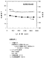
このシリコン酸化膜について、成膜直後における形成膜の比誘電率(k(1MHz))と屈折率のH2Oガス流量依存性を調査した結果を図4に示す。図4の左側の縦軸は線型目盛りで表した比誘電率を示し、右側の縦軸は線型目盛りで表した屈折率を示す。同じく、横軸はH2Oガス流量(sccm)を示す。
【0075】
比誘電率(k(1MHz))は、シリコン酸化膜に直流電圧を印加し、その直流電圧に周波数1MHzの信号を重畳したC−V測定法により容量を測定し、その容量値から算出した。また、屈折率は、エリプソメータで6328オングストロームのHe−Neレーザを用いて測定した。以下の実施例でも同じ。
【0076】
なお、屈折率を測定しているのは、以下のように、C−H、O−Hなどに起因するイオン分極及び配向分極の大きさを評価できるためである。高い周波数の光で測定しているため、イオン分極や配向分極を除いた電子分極の大きさke (屈折率nの2乗と表される。)を知ることができる。従って、上記比誘電率(k(1MHz))及び電子分極(ke)により、k(1MHz)=ke(電子分極)+ki(イオン分極)+ko(配向分極)の式から、ki(イオン分極)+ko(配向分極)の大きさを知ることができる。さらに、イオン分極kiは、FT−IRのデータからK−K変換(クラマース−クロニッヒ変換)を使って計算することができるので、配向分極koのみの大きさも知ることができる。
【0077】
図4によれば、成膜直後で、凡そ2.9とかなり低い比誘電率が得られた。比誘電率に関し、H2Oガス流量に対する依存性は小さく、H2Oガス流量200乃至1800sccmの範囲であまり変化はなかった。そのH2Oガス流量の200sccm以上という調査範囲が、低誘電率絶縁膜に関し、シリコン含有有機化合物に対するH2Oガスの流量比を4以上とした根拠である。
【0078】
なお、屈折率は、H2Oガス流量に対する依存性は小さく、1.38乃至1.39程度であり、比誘電率と屈折率の2乗(約1.9)の差は1以上有り、比較的大きい。
【0079】
(2)第2実施例
第2実施例の絶縁膜は低誘電率絶縁膜の他の一例である。試料は、第1実施例と同じ基板の上に低誘電率絶縁膜であるシリコン酸化膜を形成した。そのシリコン酸化膜は、プラズマCVD法により以下の成膜条件で形成された。C4F8ガス流量依存性を調べるため、C4F8ガス流量を変化させた。第2実施例においても、シリコン酸化膜の成膜前に、第1実施例と同様な条件で前処理を行い、銅配線の表面酸化膜を除去した。
【0080】
(成膜条件II)
(i)成膜ガス条件
HMDSOガス流量:50 sccm
H2Oガス流量:1000 sccm
C4F8ガス流量:0〜50 sccm
ガス圧力:1.5Torr
(ii)プラズマ化条件
高周波電力(13.56MHz)PHF:300W
低周波電力(380KHz)PLF:0W
(iii)基板加熱温度:375℃
(iv)成膜されたシリコン酸化膜
膜厚:500nm
このシリコン酸化膜について、成膜直後の形成膜の比誘電率(k)と屈折率のC4F8ガス流量依存性を調査した結果を図5に示す。図5の左側の縦軸は線型目盛りで表した比誘電率を示し、右側の縦軸は線型目盛りで表した屈折率を示す。同じく、横軸はC4F8ガス流量(sccm)を示す。
【0081】
図5によれば、第1実施例の成膜ガスにC4F8ガスを添加しているが、比誘電率は第1実施例とほぼ同じく、凡そ2.9であった。比誘電率に関し、C4F8ガス流量に対する依存性は少なく、C4F8ガス流量0乃至50sccmの範囲であまり変化はなかった。
【0082】
なお、屈折率は1.37乃至1.39が得られた。比誘電率と屈折率の2乗の差は第1実施例と同じ程度あり、比較的大きい。
【0083】
(3)第3実施例
第3実施例の絶縁膜は低誘電率絶縁膜の他の一例である。ここでは、成膜後のHe−H2プラスマ処理の前後での特性変動(比誘電率、屈折率)について調査した。試料は、第1実施例と同じ基板の上に低誘電率絶縁膜であるシリコン酸化膜を形成した。そのシリコン酸化膜は、プラズマCVD法により以下の成膜条件で形成された。H2Oガス流量依存性を調べるため、H2Oガス流量を変化させた。第3実施例においても、シリコン酸化膜の成膜前に、第1実施例と同様な条件で前処理を行い、銅配線の表面酸化膜を除去した。
【0084】
(成膜条件III)
(i)成膜ガス条件
HMDSOガス流量:50 sccm
H2Oガス流量:200〜1400 sccm
ガス圧力:2.0Torr
(ii)プラズマ化条件
高周波電力(13.56MHz)PHF:300W
低周波電力(380KHz)PLF:0W
(iii)基板加熱温度:200℃
(iv)成膜されたシリコン酸化膜
膜厚:700nm
(プラズマ処理条件I)
(i)雰囲気
ガス:HeにH2を3%混合させたガス(He−H2(3%)と表示)
ガス圧力:0.5Torr
(ii)プラズマ化条件
PHF:400W
(iii)基板加熱温度:375℃
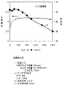
(iv)処理時間:2分
図6は、上記成膜条件IIIにより成膜したシリコン酸化膜について、上記プラズマ処理条件Iでプラズマ処理した前後での特性(比誘電率、屈折率)変動について調査した結果を示すグラフである。図6の左側の縦軸は線型目盛りで表した比誘電率を示し、右側の縦軸は線型目盛りで表した屈折率を示す。同じく、横軸はH2Oガス流量(sccm)を示す。図中、●印は成膜後、プラズマ処理前の形成膜の比誘電率を示し、○印はプラズマ処理後の形成膜の比誘電率を示す。◆印は成膜後、プラズマ処理前の形成膜の屈折率を示し、◇印はプラズマ処理後の形成膜の屈折率を示す。
【0085】
図6によれば、成膜直後の比誘電率凡そ2.9であったものが、プラズマ処理後に凡そ2.47に低減した。この場合も、比誘電率はH2Oガス流量に対する依存性は少なく、H2Oガス流量200乃至1400sccmの範囲であまり変化はなかった。このように、プラズマ処理による比誘電率低減の効果は著しい。
【0086】
一方、成膜直後の屈折率凡そ1.4であったものが、プラズマ処理後に凡そ1.51に増加した。また、H2Oガス流量に対する依存性は少なかった。従って、プラズマ処理により比誘電率と屈折率の2乗(約2.3)の差は小さくなった。この結果より、電子分極は少し増加するが、それ以上に、結合が弱いと考えられるC−HやO−Hに起因するイオン分極及び配向分極は減少していることが確認できた。即ち、プラズマ処理によりC−HやO−Hが形成膜から除去されて比誘電率が低減することを確認できた。
【0087】
(4)第4実施例
第4実施例の絶縁膜はCuバリア絶縁膜の一例である。試料は、図11に示すように、銅膜31の上にCuバリア絶縁膜であるシリコン酸化膜32を形成した。そのシリコン酸化膜32は、プラズマCVD法により以下の成膜条件で形成された。H2Oガス流量依存性を調べるため、H2Oガス流量を変化させた。第4実施例においても、シリコン酸化膜の成膜前に、第1実施例と同様な条件で銅配線の前処理を行い、表面酸化膜を除去した。
【0088】
(成膜条件IV)
(i)成膜ガス条件
HMDSOガス流量:50 sccm
H2Oガス流量:0〜2000 sccm
ガス圧力:1.0Torr
(ii)プラズマ化条件
高周波電力(13.56MHz)PHF:0W
低周波電力(380KHz)PLF:150W
(iii)基板加熱温度:375℃
(iv)成膜されたシリコン酸化膜
膜厚:50nm
このシリコン酸化膜32について、成膜直後の比誘電率(k)と屈折率のH2Oガス流量依存性を調査した結果を図7に示す。図7の左側の縦軸は線型目盛りで表した比誘電率を示し、右側の縦軸は線型目盛りで表した屈折率を示す。同じく、横軸はH2Oガス流量(sccm)を示す。
【0089】
図7によれば、H2Oガス流量が凡そ400sccmまではH2Oガス流量の増加とともに比誘電率も増加した。即ち、H2Oガス流量0sccmで比誘電率3.7であったものが、H2Oガス流量400sccmで比誘電率4.2となった。H2Oガス流量400sccmより大きい範囲では、H2Oガス流量の増加とともに比誘電率はあまり変化せず、4.2程度で推移した。
【0090】
なお、屈折率に関しては、H2Oガス流量が凡そ400sccmまではH2Oガス流量の増加とともにあまり変化せず、ほぼ1.66前後であった。しかし、H2Oガス流量400sccm以降は、H2Oガス流量の増加とともに減少した。即ち、H2Oガス流量400sccmで1.66であったものが、H2Oガス流量2000sccmで1.55となった。
【0091】
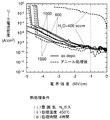
また、同じ成膜条件で作成したシリコン酸化膜について、熱処理前後でのリーク電流密度を調査した。熱処理条件は以下の通りである。
【0092】
(熱処理条件)
(i)雰囲気ガス:N2
(ii)基板加熱温度:450℃
(iii)処理時間:4時間
その結果を図8に示す。図8の縦軸は対数目盛りで表したリーク電流密度(A/cm2)を示し、横軸は線型目盛りで表した電界強度(MV/cm)を示す。その電界強度は印加した電圧より換算したものである。
【0093】
図8によれば、Cuに対する拡散阻止能力は成膜時のH2Oガス流量に依存することが確認できた。即ち、成膜時のH2Oガス流量400sccmの場合、熱処理前には高い電界強度まで急激に立ち上がる現象は見られなかったが、熱処理後には電界強度が低いところで、急激に立ち上がる現象が見られた。このことはCuの拡散により形成膜の絶縁性がなくなっていることを示している。これに対して、成膜時のH2Oガス流量600sccm以上では、そのような現象は観察されず、形成膜はCuの拡散阻止能力を保持していることを示している。そのH2Oガス流量600sccm以上という範囲が、Cuバリア絶縁膜の成膜ガスに関し、シリコン含有有機化合物に対するH2Oガスの流量比を12以上とした根拠である。
【0094】
(5)第5実施例
第5実施例の絶縁膜はCuバリア絶縁膜の他の一例である。試料は、第4実施例と同じく銅膜31の上にCuバリア絶縁膜であるシリコン酸化膜32aを形成した。そのシリコン酸化膜32aは、プラズマCVD法により以下の成膜条件で形成された。C2H4ガス流量依存性を調べるため、C2H4ガス流量を変化させた。第3実施例においても、シリコン酸化膜の成膜前に、第1実施例と同様な条件で銅配線の前処理を行い、表面酸化膜を除去した。
【0095】
(成膜条件V)
(i)成膜ガス条件
HMDSOガス流量:50 sccm
H2Oガス流量:1000 sccm
C2H4ガス流量:0〜300 sccm
ガス圧力:1.0Torr
(ii)プラズマ化条件
高周波電力(13.56MHz)PHF:0W
低周波電力(380KHz)PLF:150W
(iii)基板加熱温度:375℃
(iv)成膜されたシリコン酸化膜
膜厚:50nm
このシリコン酸化膜32aについて、比誘電率(k)と屈折率の成膜時のC2H4ガス流量依存性を調査した結果を図9に示す。図9の左側の縦軸は線型目盛りで表した比誘電率を示し、右側の縦軸は線型目盛りで表した屈折率を示す。同じく、横軸はC2H4ガス流量(sccm)を示す。
【0096】
図9によれば、成膜時のC2H4ガス流量に対して比誘電率はあまり変化せず、4.3乃至4.4程度で推移した。なお、屈折率に関しては、C2H4ガス流量の増加とともに増大した。即ち、C2H4ガス流量0sccmで1.62であったものが、C2H4ガス流量300sccmで1.71となった。
【0097】
また、同じ成膜条件で作成したシリコン酸化膜について、熱処理前後でのリーク電流密度を調査した。熱処理条件は第4実施例と同じとした。
【0098】
その結果を図10に示す。図10の縦軸は対数目盛りで表したリーク電流密度(A/cm2)を示し、横軸は線型目盛りで表した電界強度(MV/cm)を示す。
【0099】
図10によれば、C2H4ガス流量0sccm以外は熱処理前より、リーク電流密度が急激な立ち上がりをする電界強度は低下したが、ダメージとなる程度ではなく、Cuに対する拡散阻止能力は成膜時のC2H4ガス流量に依存しないことが確認できた。
【0100】
(6)第6実施例
第6実施例の絶縁膜はCuバリア絶縁膜の一例である。試料は、第4実施例と同じく銅膜31の上にCuバリア絶縁膜であるシリコン酸化膜32を形成した。そのシリコン酸化膜32は、プラズマCVD法により以下の成膜条件で形成された。第6実施例においても、シリコン酸化膜の成膜前に、第1実施例と同様な条件で銅配線の前処理を行い、表面酸化膜を除去した。
【0101】
(成膜条件VI)
(i)成膜ガス条件
HMDSOガス流量:50 sccm
H2Oガス流量:1000 sccm
ガス圧力:1.0Torr
(ii)プラズマ化条件
高周波電力(13.56MHz)PHF:300W
低周波電力(380KHz)PLF:25W
(iii)基板加熱温度:375℃
(iv)成膜されたシリコン酸化膜
膜厚:50nm
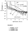
このシリコン酸化膜32について、成膜直後の比誘電率(k)を調査した結果、3.9であった。
【0102】
また、同じ成膜条件で作成したシリコン酸化膜について、熱処理前後でのリーク電流密度を調査した。熱処理条件は以下の通りである。
【0103】
(熱処理条件)
(i)雰囲気ガス:N2
(ii)基板加熱温度:450℃
(iii)処理時間:4時間
その結果を図15に示す。図15の縦軸は対数目盛りで表したリーク電流密度(A/cm2)を示し、横軸は線型目盛りで表した電界強度(MV/cm)を示す。その電界強度は印加した電圧より換算したものである。
【0104】
図15によれば、リーク電流は1MV/cmで10−10〜10−9A/cm2と極めて小さく、かつ絶縁破壊耐性も十分に高い。Cuに対する拡散阻止能力が高いことを確認することができた。また、Cuに対する拡散阻止能力に対する成膜時のH2Oガス流量依存性は上記実施例と同様と考えられる。即ち、シリコン含有有機化合物に対するH2Oガスの流量比を12以上とする範囲が好適である。
(第2の実施の形態)
次に、図12(a)〜(c)、図13(a)、(b)、及び図14(a)、(b)を参照して、本発明の第2の実施の形態に係る半導体装置及びその製造方法を説明する。
【0105】
図14(b)は、本発明の第2の実施の形態に係る半導体装置を示す断面図である。この半導体装置は、同図に示すように、基板61上に下部配線埋込絶縁膜62が形成されている。下部配線埋込絶縁膜62は、膜厚約500nmのSiO2 膜からなる低誘電率を有する主たる絶縁膜(低誘電率絶縁膜)62aと、膜厚約50nmのSiO2 膜からなる第1の上部保護層(Cuバリア絶縁膜)63aとが積層されてなる。下部配線埋込絶縁膜62を貫通する下部配線溝64に銅拡散阻止膜であるTaN膜65aと銅膜65bとからなる下部配線65が埋め込まれている。基板61は半導体基板や他の導電層でもよいし、絶縁性基板でもよい。
【0106】
これらの上にビアホール68が形成された配線層間絶縁膜66と上部配線溝69が形成された上部配線埋込絶縁膜67が形成されている。
【0107】
配線層間絶縁膜66は膜厚約50nmのSiO2 膜からなる第2の下部保護層(Cuバリア絶縁膜)66aと、膜厚約500nmのSiO2 膜からなる低誘電率を有する主たる絶縁膜(低誘電率絶縁膜)66bと、膜厚約50nmのSiO2 膜からなる第2の上部保護層(Cuバリア絶縁膜)66cとから構成されている。上部配線埋込絶縁膜67は、膜厚約500nmのSiO2 膜からなる低誘電率を有する主たる絶縁膜(低誘電率絶縁膜)67aと、膜厚約50nmのSiO2 膜からなる第3の上部保護層(Cuバリア絶縁膜)67bとから構成されている。
【0108】
上部配線溝69はビアホール68よりも大きい開口面積を有し、ビアホール68と接続するように形成されている。ビアホール68と上部配線溝69内には、よく知られたデュアルダマシン法により銅拡散阻止膜であるTaN膜70aと銅膜70bとからなる接続導体70と同じく銅拡散阻止膜であるTaN膜70aと銅膜70bとからなる上部配線71が一体的に埋め込まれている。そして、最上部全面はこの発明に係るSiO2 膜からなる最上部保護層(Cuバリア絶縁膜)72によって被覆されている。
以上の低誘電率絶縁膜及びCuバリア絶縁膜はすべて本発明に係る絶縁膜である。
【0109】
次に、図12(a)〜(c)、図13(a)、(b)、及び図14(a)、(b)を参照して本発明の第2の実施の形態に係る半導体装置の製造方法を説明する。図1の成膜装置を用いるものとする。
【0110】
まず、図12(a)に示すように、成膜装置のチャンバ1内に基板61を搬入し、基板61上に、低誘電率を有する膜厚約500nmのSiO2膜62を形成する。SiO2膜62は下部配線埋込絶縁膜の主たる絶縁膜となる。成膜ガス条件は、シロキサン結合を有するシリコン含有有機化合物、例えばHMDSOガス流量を50 sccm、H2Oガス流量を1000 sccmとし、そのガス圧力を1.75Torrとする。成膜ガスのプラズマ化条件は、周波数380kHzの低周波電力(PLF)を印加せず、周波数13.56MHzの高周波電力(PHF)を300W印加する。また、基板温度を375℃とする。この成膜条件は、第1の実施の形態の第1実施例の成膜条件Iに相当する。さらに、成膜後、第3実施例の形成膜に対するプラズマ処理、又は窒素或いは不活性ガス雰囲気中での形成膜に対するアニール処理と、形成膜の表面層除去処理と、減圧中でのCH3基を有する処理ガスによる形成膜に対する耐水性処理とを同じチャンバ1内で行う。なお、下記するように引き続きバリア絶縁膜を形成する場合、耐水性処理は適宜省略することも可能である。
引き続き、大気に曝さないで、同じチャンバ1内で、成膜ガスとしてシロキサン結合を有するシリコン含有有機化合物、例えばHMDSOガスとH2Oを用いたプラズマCVD法により、膜厚約50nmのSiO2膜(Cuバリア絶縁膜)63を形成する。成膜ガス条件は、HMDSOガス流量を50 sccm、H2Oガス流量を1000 sccmとし、そのガス圧力を1.0Torrとする。成膜ガスのプラズマ化条件は、周波数13.56MHzの高周波電力(PHF)を印加せず、周波数380kHzの低周波電力(PLF)を150W印加する。また、基板温度を375℃とする。この成膜条件は、第1の実施の形態の第4実施例の成膜条件IVに相当する。成膜されたSiO2膜63は、周波数1MHzで測定した比誘電率が凡そ4.2であり、電界強度4MV/cmのときリーク電流が10−6A/cm2であった。
【0111】
次いで、チャンバ1内から基板61を外部に取り出し、SiO2膜63上に化学増幅レジストなどからなるレジスト膜を形成する。次いで、フォトリソグラフィ法により配線溝を形成すべき領域にレジスト膜の開口部を形成し、図12(b)に示すように、マスク73aを形成する。このとき、SiO2膜63は窒素を含まないので、レジスト膜73aの架橋反応は窒素による過剰な架橋反応が抑制されて露光範囲により決まる領域だけに生じるため、寸法精度の良いマスク73aを形成することができる。次いで、図12(b)に示すように、マスク73aに基づいてSiO2膜63及び62をエッチングして配線溝64を形成する。SiO2膜63aは保護層となる。
【0112】
次に、図12(c)に示すように、配線溝64の内面に銅拡散阻止膜としてTaN膜65aを形成する。続いて、図示しない銅シード層を形成した後、銅膜65bを埋め込んで、TaN膜及びTa膜65aと、銅膜65bとからなる下部配線65を形成する。
【0113】
次いで、成膜前に、銅膜65b表面の前処理を行い、表面酸化膜を除去した。その処理方法は、平行平板型プラズマ励起CVD装置を用い、NH3を流量500sccmで導入してガス圧力を1Torrに調整し、周波数13.56MHzの電力を印加してNH3をプラズマ化し、基板61を375℃に加熱した状態で銅膜65bをそのプラズマに接触させる。
次に、成膜装置のチャンバ1内に基板61を搬入し、図13(a)に示すように、下部配線65を被覆するSiO2 膜からなる保護層(Cuバリア絶縁膜)66aを形成する。保護層66aに関し、成膜条件は、HMDSOガス流量を50 sccm、H2Oガス流量を1000 sccm、C2H4ガス流量を100sccmとし、そのガス圧力を1.0Torrとする。成膜ガスのプラズマ化条件は、周波数13.56MHzの高周波電力(PHF)を印加せず、周波数380kHzの低周波電力(PLF)を150W印加する。また、基板温度を375℃とする。この成膜条件は、第1の実施の形態の第5実施例の成膜条件Vに相当する。
その後、この保護層66a上に、配線層間絶縁膜66の主たる絶縁膜となる、膜厚約500nmのSiO2 膜からなる絶縁膜(低誘電率絶縁膜)66b、及び膜厚約50nmのSiO2 膜からなる保護層(Cuバリア絶縁膜)66cを、同じチャンバ1内で連続形成し、接続導体を埋め込むための配線層間絶縁膜66を形成する。
主たる絶縁膜66bに関し、下部配線埋込絶縁膜62の成膜条件、及び成膜後の膜の処理条件と同じとする。また、保護層66cに関し、保護層66aの成膜条件と同じとする。
続いて、同じようにして保護層66c上に配線埋込絶縁膜の主たる絶縁膜となる、SiO2 膜からなる絶縁膜(低誘電率絶縁膜)67a、及びSiO2 膜からなる保護層(Cuバリア絶縁膜)67bを同じチャンバ1内で連続形成し、上部配線を埋め込む配線埋込絶縁膜67を形成する。主たる絶縁膜67aに関し、下部配線埋込絶縁膜62の成膜条件、及び成膜後の膜の処理条件と同じとする。保護層67bに関し、保護層66aの成膜条件と同じとする。
【0114】
次に、成膜装置のチャンバ1内から基板61を外部に取り出し、図13(b)乃至図14(b)に示すように、良く知られたデュアルダマシン法により、接続導体70と上部配線71を形成する。以下に、デュアルダマシン法を詳細に説明する。
【0115】
即ち、保護層67b上にレジスト膜を形成した後、フォトリソグラフィー法によりビアホールを形成すべき領域にレジスト膜の開口部を形成し、図13(b)に示すように、マスク73bを形成する。このとき、保護層67bは窒素を含まないので、レジスト膜73bの架橋反応は窒素による過剰な架橋反応が抑制されて露光範囲により決まる領域だけに生じるため、寸法精度の良いマスク73bを形成することができる。
次いで、レジスト膜73bの開口部を通して保護層67b及び絶縁膜67a、保護層66c及び絶縁膜66bをエッチングし、貫通させる。これにより、配線層間絶縁膜66のうち保護層66c及び主たる絶縁膜66bに開口部68が形成される。
【0116】
次に、保護層67b上に別のレジスト膜を形成し、配線溝を形成すべき領域に開口部を形成し、図14(a)に示すように、マスク73cを形成する。このとき、保護層67b、絶縁膜67a、保護層66c、絶縁膜66b及び保護層66aは窒素を含まないので、レジスト膜73cの架橋反応は窒素による過剰な架橋反応が抑制されて露光範囲により決まる領域だけに生じるため、寸法精度の良いマスク73cを形成することができる。
次いで、このマスク73cの開口部は最初の開口部の開口面積よりも大きく、かつ最初の開口部を含むように形成される。次いで、マスク73cの開口部を通して保護層67b及び絶縁膜67aをエッチングし、貫通させる。このとき、下地の保護層66cはC2H4ガスを含む成膜ガスにより成膜されているので、主たる絶縁膜67aのエッチングガスに対してエッチング耐性を有し、このため、保護層66cでエッチングが停止される。これにより、配線埋込絶縁膜67に配線溝69が形成される。その後、保護層66aをエッチングして、配線層間絶縁膜66を貫通するビアホール68を形成する。これにより、ビアホール68底部に下部配線65が露出し、ビアホール68を通して下部配線65と配線溝69とが繋がる。
【0117】
次に、図14(b)に示すように、TaN膜及びTa膜70aをビアホール68と配線溝69の内面に形成した後、図示しない銅シード層を形成し、更にその上に銅膜70bを埋め込んで、接続導体70と上部配線71を形成する。以上が所謂デュアルダマシン法である。
【0118】
次に、成膜前に、銅膜65b表面の前処理条件と同じ条件で、銅膜70b表面の前処理を行い、表面酸化膜を除去した。次いで、保護層63又は66aと同じ成膜方法により、全面にSiO2 膜からなる保護層72を形成する。以上により、銅膜を主とする多層配線を有する半導体装置が完成する。
【0119】
以上のように、この第2の実施の形態の半導体装置の製造方法によれば、主たる絶縁膜62a、66b、67aは、第1の実施の形態の第1実施例の成膜条件Iで成膜し、成膜後にプラズマ処理又はアニール処理と、表面層除去処理と、耐水性処理とを行っている。即ち、第1の実施の形態の第3実施例類似の成膜条件で作成されているため、主たる絶縁膜62a、66b、67aは2.5以下の低誘電率を有し、かつ耐湿性が高くなっている。また、保護層63a、66a、66c、67b、72は第1の実施の形態の第4及び第5実施例の成膜条件IV又はVで形成されているため、Cuに対して高い拡散阻止能力を有する。
しかも、表面に露出する絶縁膜66b、67aや保護層66a、66c、67bが窒素を含まないので、フォトリソグラフィ法により下部配線溝64、ビアホール68、及び上部配線溝69を形成する際に、寸法精度の良いマスク73cを形成することができる。
さらに、配線層間絶縁膜66及び配線埋込絶縁膜67を下から順に開口面積が大きくなるように貫通させて、ビアホール68とビアホール68と繋がった配線溝69とを交互に形成している。即ち、保護層66cは主たる絶縁膜67aを選択的にエッチングする際にエッチングされる絶縁膜67aの下地となる。この発明が適用される保護層66cはC2H4を含む成膜ガスにより形成されているため、主たる絶縁膜67aのエッチャントに対してエッチングストッパとして有効に機能するとともに、下層の絶縁膜66bの過剰エッチングに対するマスクとして有効に機能する。
【0120】
(第3の実施の形態)
次に、本発明の第3の実施の形態に係る半導体装置及びその製造方法を説明する。
図14(b)の半導体装置と類似の構造を、第3の実施の形態に係る半導体装置に適用することができる。
この場合、主たる絶縁膜62a、66b、67aが本実施形態の低誘電率絶縁膜に対応し、保護層63a、66a、66c、67b、72が本実施形態のバリア絶縁膜に対応する。
また、図12(a)〜(c)、図13(a)、(b)、及び図14(a)、(b)の半導体装置の製造方法と類似の方法を、第3の実施の形態に係る半導体装置の製造方法に適用することができる。
この場合、主たる絶縁膜62a、66b、67aに対応する低誘電率絶縁膜は下記の成膜条件で成膜する。
【0121】
(成膜条件)
(i)成膜ガス条件
HMDSOガス流量:50 sccm
H2Oガス流量:1000 sccm
ガス圧力:2.0Torr
(ii)プラズマ化条件
高周波電力(13.56MHz)PHF:300W
低周波電力(380KHz)PLF:0W
(iii)基板加熱温度:300℃
(iv)成膜されたシリコン酸化膜
膜厚:700nm
成膜後にプラズマ処理又はアニール処理と、表面層の除去処理と、耐水性処理とを行う。また、保護層63a、66a、66c、67b、72に対応するバリア絶縁膜は第1の実施の形態の第6実施例の成膜条件VIで形成する。
【0122】
以上のような本発明の第3の実施の形態によれば、上記成膜条件で低誘電率絶縁膜成膜し、成膜後にプラズマ処理又はアニール処理と、表面層の除去処理と、耐水性処理とを行うため、低誘電率絶縁膜は2.4前後の低誘電率を有し、かつ耐湿性が高くなっている。また、バリア絶縁は第1の実施の形態の第6実施例の成膜条件VIで形成されるため、Cuに対して高い拡散阻止能力を有する。
【0123】
以上、実施の形態によりこの発明を詳細に説明したが、この発明の範囲は上記実施の形態に具体的に示した例に限られるものではなく、この発明の要旨を逸脱しない範囲の上記実施の形態の変更はこの発明の範囲に含まれる。
【0124】
例えば、第2の実施の形態では、主たる絶縁膜(低誘電率絶縁膜)62a、66b、67aの成膜条件を、第1の実施の形態における第1実施例と第3実施例に記載の条件としているが、第1の実施の形態で説明した成膜条件の範囲で適宜変更して適用することができる。また、第3の実施の形態における、主たる絶縁膜(低誘電率絶縁膜)62a、66b、67aの成膜条件は、第1の実施の形態で説明した成膜条件の範囲で適宜変更して適用することができる。
【0125】
また、保護層(Cuバリア絶縁膜)63a、66a、66c、67b、72の成膜条件を、第1の実施の形態における第4実施例、第5実施例、第6実施例に記載の条件としているが、第1の実施の形態で説明した成膜条件の範囲で適宜変更して適用することができる。
【0126】
【発明の効果】
以上のように、本発明によれば、低誘電率絶縁膜の成膜において、シロキサン結合を有するシリコン含有有機化合物又はCH3 基を有するシリコン含有有機化合物のうち何れか一とH2Oを含み、シリコン含有有機化合物に対するH2Oの流量比を4以上に、かつガス圧力を1.5Torr以上になるように調整して成膜ガスを生成し、その成膜ガスに好ましくは周波数1MHz以上の高周波電力を印加してプラズマを生成し、好ましくは400℃以下に加熱した基板上に成膜している。さらに、成膜後、He等に好ましくは周波数1MHz未満の電力を印加してプラズマを生成し、そのプラズマにより形成膜に対してプラズマ処理し、又は窒素ガス等を用いて400℃以上の温度でアニール処理している。これにより、低誘電率絶縁膜において、2.4乃至2.5と低い比誘電率を維持しつつ、窒素を含まないようにし、或いはレジストの架橋反応に影響を与えない程度に窒素含有量を抑制することができる。さらに、形成膜の表面層を除去した後に露出した吸湿性が高い可能性がある膜に対して、CH3基を有する処理ガスの減圧雰囲気中で加熱する耐水性処理を行うことにより、さらに、耐湿性に優れた特性を得ることができる。
【0127】
また、低誘電率絶縁膜とともに用いるCuバリア絶縁膜においては、シロキサン結合を有するシリコン含有有機化合物又はCH3 基を有するシリコン含有有機化合物のうち何れか一とH2Oを含み、シリコン含有有機化合物に対するH2Oの流量比を12以上と高めて成膜ガスを生成し、好ましくは周波数1MHz以下の低周波電力で基板バイアスするとともにその成膜ガスに印加してプラズマを生成し、200乃至400℃に昇温した基板上に成膜している。以上の成膜条件とすることで、Cuの拡散を阻止する機能を高めた、さらに膜質の良い膜を形成しつつ、窒素を含まないようにし、或いはレジストの架橋反応に影響を与えない程度に窒素含有量を抑制することができる。
【図面の簡単な説明】
【図1】本発明の第1の実施の形態である半導体装置の製造方法に用いられるプラズマCVD装置の構成を示す側面図である。
【図2】本発明の第1の実施の形態である半導体装置の製造方法に用いられる低誘電率絶縁膜、及びCuバリア絶縁膜の成膜工程について示すフローチャートである。
【図3】本発明の第1の実施の形態である半導体装置の製造方法に用いられる低誘電率絶縁膜、及びCuバリア絶縁膜の成膜ガスに関し、特に有効なガスの組み合わせについて示す表である。
【図4】本発明の第1の実施の形態である半導体装置の製造方法に係る、第1実施例の成膜条件Iで形成されたシリコン酸化膜に関し、その比誘電率及び屈折率のH2O依存性を示すグラフである。
【図5】本発明の第1の実施の形態である半導体装置の製造方法に係る、第2実施例の成膜条件IIで形成されたシリコン酸化膜に関し、その比誘電率及び屈折率のC4F8依存性を示すグラフである。
【図6】本発明の第1の実施の形態である半導体装置の製造方法に係る、第3実施例の成膜条件IIIで形成されたシリコン酸化膜に関し、成膜後のプラズマ処理前後におけるその比誘電率及び屈折率のH2O依存性を示すグラフである。
【図7】本発明の第1の実施の形態である半導体装置の製造方法に係る、第4実施例の成膜条件IVで形成されたシリコン酸化膜に関し、その比誘電率及び屈折率のH2O依存性を示すグラフである。
【図8】本発明の第1の実施の形態である半導体装置の製造方法に係る、第4実施例の成膜条件IVで形成されたシリコン酸化膜に関し、加熱処理前後におけるリーク電流密度の電界強度依存性を示すグラフである。
【図9】本発明の第1の実施の形態である半導体装置の製造方法に係る、第5実施例の成膜条件Vで形成されたシリコン酸化膜に関し、その比誘電率及び屈折率のC2H4依存性を示すグラフである。
【図10】本発明の第1の実施の形態である半導体装置の製造方法に係る、第5実施例の成膜条件Vで形成されたシリコン酸化膜に関し、加熱処理前後におけるリーク電流密度の電界強度依存性を示すグラフである。
【図11】本発明の第1の実施の形態である半導体装置の製造方法に係る、第4、第5実施例に用いた試料の構造を示す断面図である。
【図12】(a)乃至(c)は、本発明の第2及び第3の実施の形態の半導体装置及びその製造方法について示す断面図(その1)である。
【図13】(a)、(b)は、本発明の第2及び第3の実施の形態の半導体装置及びその製造方法について示す断面図(その2)である。
【図14】(a)、(b)は、本発明の第2及び第3の実施の形態の半導体装置及びその製造方法について示す断面図(その3)である。
【図15】本発明の第1の実施の形態である半導体装置の製造方法に係る、第6実施例の成膜条件VIで形成されたシリコン酸化膜に関し、加熱処理前後におけるリーク電流密度の電界強度依存性を示すグラフである。
【符号の説明】
1 チャンバ
2 上部電極
3 下部電極
4 排気配管
5 バルブ
6 排気装置
7 高周波電力供給電源(RF電源)
8 低周波電力供給電源
9a 配管
9b〜9h 分岐配管
10a〜10o 開閉手段
11a〜11g 流量調整手段
12 ヒータ
21 基板
31 銅膜
32、32a シリコン酸化膜
61 下地基板
62 下部配線埋込絶縁膜
62a、66b、67a 主たる絶縁膜(低誘電率絶縁膜)
63a、66a、66c、67b 保護層(Cuバリア絶縁膜)
64 下部配線溝
65 下部配線
65b、70b 銅膜
66 配線層間絶縁膜
67 上部配線埋込絶縁膜
68 開口部
69 上部配線溝
73a、73b、73c マスク
101 成膜装置
101A 成膜部
101B 成膜ガス及び処理ガス供給部[0001]
TECHNICAL FIELD OF THE INVENTION
The present invention relates to a semiconductor device and a method of manufacturing the same, and more particularly, to a semiconductor device having a low dielectric constant insulating film or a barrier insulating film formed by covering a Cu wiring and a method of manufacturing the same.
[0002]
[Prior art]
In recent years, as the degree of integration and the density of semiconductor integrated circuit devices have been increased, higher data transfer speeds have been demanded. For this reason, an insulating film having a small RC delay time and a low dielectric constant (hereinafter referred to as a low dielectric constant insulating film) is used.
[0003]
When a low dielectric constant insulating film is used as the interlayer insulating film covering the Cu wiring, since the low dielectric constant insulating film has porosity, Cu is easily diffused, and there is a possibility that the insulating property may be deteriorated. Therefore, an insulating film (hereinafter, referred to as a barrier insulating film) for preventing the diffusion of Cu is often used between the low dielectric constant insulating film and the Cu wiring.
[0004]
Regarding the low dielectric constant insulating film, a silicon-containing organic compound and N2A film is formed by a plasma CVD method using a film forming gas containing O,2It is made porous by performing plasma treatment or the like. As for the barrier insulating film, a silicon-containing organic compound and N2The film is formed by a plasma CVD method using a film forming gas containing O. Alternatively, a silicon-containing organic compound and N2O plus N2And NH3The film is formed by a plasma CVD method using a film forming gas to which a gas or the like is added.
[0005]
[Problems to be solved by the invention]
However, in the low-dielectric-constant insulating film and the barrier insulating film, nitrogen introduced into the film due to a film-forming gas containing nitrogen is problematic. Hereinafter, the problem caused by nitrogen will be described in detail.
[0006]
KrF or ArF which exposes a line width of 0.13 μm or less when forming a via hole or a wiring groove by a dual damascene method in a low dielectric constant insulating film and a barrier insulating film formed by a film forming gas containing nitrogen. When a chemically amplified resist is used, there is a problem that a pattern as designed cannot be formed. According to various investigations, it is presumed that this phenomenon is caused by release of nitrogen in the low dielectric constant insulating film or the barrier insulating film, which causes excessive crosslinking reaction of the resist. In particular,
[0007]
The present invention has been made in view of the above-described problems of the conventional example. In forming a low-dielectric-constant insulating film or a barrier insulating film, while maintaining the functions of the respective films, nitrogen is contained in the formed film. And a method for manufacturing a semiconductor device capable of suppressing the nitrogen content to such an extent as not to affect the crosslinking reaction of a resist, and a semiconductor device manufactured by the method.
[0008]
[Means for Solving the Problems]
In order to solve the above problems, the invention according to
According to a second aspect of the present invention, there is provided the method of manufacturing a semiconductor device according to the first aspect, wherein the power applied to the film forming gas is a power having a frequency of 1 MHz or more,
According to a third aspect of the present invention, there is provided the method for manufacturing a semiconductor device according to any one of the first and second aspects, wherein the power applied to the processing gas is a power having a frequency of less than 1 MHz,
According to a fourth aspect of the present invention, there is provided the method for manufacturing a semiconductor device according to any one of the first and second aspects, wherein the power applied to the processing gas is power having a frequency of 1 MHz or more,
According to a fifth aspect of the present invention, there is provided the method of manufacturing a semiconductor device according to any one of the first to fourth aspects, wherein a pressure of the processing gas is adjusted to 1.0 Torr or less,
According to a sixth aspect of the present invention, there is provided the method of manufacturing a semiconductor device according to any one of the first to fourth aspects, wherein the pressure of the processing gas is adjusted to 0.5 Torr or less,
According to a seventh aspect of the present invention, there is provided the method of manufacturing a semiconductor device according to any one of the first to sixth aspects, wherein the step of contacting the low-dielectric-constant insulating film with the plasma of the processing gas comprises the step of: Characterized in that the temperature of the insulating film is raised to 375 ° C. or higher,
The invention according to
According to a ninth aspect of the present invention, there is provided the method of manufacturing a semiconductor device according to the eighth aspect, wherein after removing a surface layer of the low dielectric constant insulating film, the low dielectric constant insulating film is continuously exposed without being exposed to the atmosphere. The temperature of the low dielectric constant insulating film is increased to 375 ° C. or more under atmospheric pressure or reduced pressure, and CH3Characterized by having a step of contacting with a processing gas having a group,
The invention according to
According to an eleventh aspect of the present invention, in the method of manufacturing a semiconductor device according to the tenth aspect, the electric power applied to the film forming gas is an electric power having a frequency of 1 MHz or more,
According to a twelfth aspect of the present invention, in the method of manufacturing a semiconductor device according to the tenth or eleventh aspect, after the step of heat-treating the low dielectric constant insulating film, the surface layer of the low dielectric constant insulating film is removed. Characterized by
According to a thirteenth aspect of the present invention, in the method of manufacturing a semiconductor device according to the twelfth aspect, after removing a surface layer of the low dielectric constant insulating film, the low dielectric constant insulating film is continuously exposed without being exposed to the atmosphere. The temperature of the low dielectric constant insulating film is increased to 375 ° C. or more under atmospheric pressure or reduced pressure, and CH3Characterized by having a step of contacting with a processing gas having a group,
The invention according to
According to a fifteenth aspect of the present invention, there is provided the method of manufacturing a semiconductor device according to any one of the first to fourteenth aspects, wherein a pressure of the film forming gas is adjusted to 1.75 Torr or more,
According to a sixteenth aspect of the present invention, in the method of manufacturing a semiconductor device according to any one of the first to fifteenth aspects, in the step of forming the low dielectric constant insulating film, the substrate is set at 25 ° C. or more and 400 ° C. or less. Characterized in that the temperature rises to
The invention according to claim 17 relates to a method for manufacturing a semiconductor device, comprising a silicon-containing organic compound having a siloxane bond or CH.3 Any one of the silicon-containing organic compounds having a group2O and the H with respect to the silicon-containing organic compound.2A process of generating a film forming gas by setting the flow ratio of O to 12 or more, a process of raising the temperature of the substrate to 200 ° C. or more and 400 ° C. or less, and generating a plasma by applying power to the film forming gas; Forming a barrier insulating film on the heated substrate.
According to an eighteenth aspect of the present invention, in the method of manufacturing a semiconductor device according to the seventeenth aspect, in the step of generating the film forming gas, the pressure of the film forming gas is adjusted to less than 1.0 Torr, and the barrier insulating film is formed. Forming a barrier insulating film by applying a power of less than 1 MHz to the substrate to bias the substrate and generating a plasma of the film-forming gas with the power of less than 1 MHz in the step of forming and reacting the same. Characterized by
According to a nineteenth aspect of the present invention, in the method of manufacturing a semiconductor device according to the seventeenth aspect, in the step of generating the film forming gas, the pressure of the film forming gas is adjusted to 1.0 Torr or more, and the barrier insulating film is formed. In the forming step, a power of less than 1 MHz is applied to the substrate to bias the substrate, and at least the power of 1 MHz or more of the power of less than 1 MHz or the power of 1 MHz or more is applied to the pressure of 1.0 Torr. It is characterized in that a plasma is generated by applying to the film-forming gas adjusted as described above, and is reacted to form a barrier insulating film.
The invention according to
According to a twenty-first aspect of the present invention, there is provided the method for manufacturing a semiconductor device according to any one of the seventeenth to twentieth aspects, wherein the film forming gas includes dinitrogen monoxide (N2O) or nitrogen (N2) Or ammonia (NH3) Or dinitrogen monoxide (N2O) and ammonia (NH3) Is added,
The invention according to claim 22 relates to the method for manufacturing a semiconductor device according to any one of
[0009]
Embedded image
Octamethyltrisiloxane (OMTS)
[0011]
Embedded image
Or, tetramethylcyclotetrasiloxane (TMCTS)
[0013]
Embedded image
Characterized by any one of the following,
The invention according to claim 23 relates to the method for manufacturing a semiconductor device according to any one of
[0015]
Embedded image
Octamethyltrisiloxane (OMTS)
[0017]
Embedded image
Or, tetramethylcyclotetrasiloxane (TMCTS)
[0019]
Embedded image
At least one CH of any one of3A compound in which the group is replaced by F,
The invention according to claim 24 relates to the method of manufacturing a semiconductor device according to any one of
According to a twenty-fifth aspect of the present invention, there is provided the method for manufacturing a semiconductor device according to any one of the first to twenty-fourth aspects, wherein the film-forming gas includes CxHy(X and y are positive integers), CxHyFzOr CxHyBz(X and y are 0 (however, excluding x = y = 0) or a positive integer, z is a positive integer),
The invention according to claim 26 relates to the method of manufacturing a semiconductor device according to claim 25, wherein the CxHyIs C2H4Characterized in that
The invention according to claim 27 relates to the method of manufacturing a semiconductor device according to claim 25, wherein the CxHyFzIs C3F8, C4F8Or CHF3Characterized in that
The invention according to claim 28 relates to the method of manufacturing a semiconductor device according to claim 25, whereinxHyBzIs B2H6Characterized in that
The invention according to claim 29 relates to a method for manufacturing a semiconductor device, a step of forming a low dielectric constant insulating film by the method for manufacturing a semiconductor device according to
The invention according to
The invention according to claim 31 is directed to the method of manufacturing a semiconductor device according to claim 29 or 30, wherein after the step of forming the low dielectric constant insulating film, the low dielectric constant insulating film is continuously exposed without being exposed to the atmosphere. Performing a step of forming the barrier insulating film,
The invention according to claim 32 is directed to the method of manufacturing a semiconductor device according to any one of
A thirty-third aspect of the present invention relates to a semiconductor device, characterized by being produced by the method of manufacturing a semiconductor device according to any one of the first to thirty-second aspects.
[0021]
Hereinafter, the operation based on the configuration of the present invention will be described.
[0022]
According to the present invention, as the oxidizing gas, N2H instead of O2Since O is used, nitrogen is not contained in the formed film. O2Without using other oxidizing gas that does not contain nitrogen.2O is used because a film having relatively good film quality can be formed. In particular, H for organic compounds containing silicon2When the flow rate ratio of O is increased to, for example, 4 or more, a film having better film quality can be formed.
[0023]
On the other hand, H for silicon-containing organic compounds2Increasing the flow rate ratio of O tends to increase the relative dielectric constant (k). In order to suppress this, when a low dielectric constant insulating film is formed by a plasma CVD method, the plasma forming frequency of the film forming gas is increased to 1 MHz or more, and the gas pressure is increased to 1.5 Torr or more. Preferably, it is 1.75 Torr or more. Further, for the same reason, the substrate temperature is lowered to 400 ° C. or less during the film formation.
[0024]
In this case, since the formed film contains a large amount of C—H or O—H, which is considered to be weakly bonded, the relative dielectric constant is 2.6 to 2.7, which is still smaller than that of the SOD film (Spin On Dielectrics). high. Therefore, after film formation, plasma treatment or annealing treatment is performed on the formed film to discharge CH and OH.
[0025]
In the plasma processing, for example, He, Ar, H2Alternatively, a processing gas containing at least one of deuterium is generated. Further, the gas pressure is adjusted to, for example, 1 Torr or less, preferably 0.5 Torr or less. Then, electric power is applied to the processing gas to generate plasma. The plasma of the processing gas is brought into contact with the low dielectric constant insulating film heated to a temperature of 375 ° C. or higher (preferably in a range of 400 to 450 ° C.). According to the survey, He, Ar, H2Alternatively, by using plasma generated by applying power to a processing gas containing at least one of deuterium, the relative dielectric constant of a formed film can be further reduced. In particular, it is more effective to use plasma generated by applying a power of less than 1 MHz to the processing gas whose gas pressure is adjusted to 1 Torr or less. Further, the reason why the temperature of the low-dielectric-constant insulating film is raised to 375 ° C. or higher during the processing is to sufficiently discharge moisture and the like in the film which cannot be completely discharged by plasma.
[0026]
In the annealing treatment, the low dielectric constant insulating film is heated at a temperature of 400 ° C. or more in an atmosphere of a nitrogen gas or an inert gas. The reason why the annealing is performed in an atmosphere of nitrogen gas or inert gas is to prevent oxidation of the film. The reason why the annealing is performed at a temperature of 400 ° C. or more is to sufficiently discharge moisture and the like in the film without using plasma.
[0027]
After the plasma treatment or the annealing treatment, the surface of the formed film has a high density and a high density, and has a high relative dielectric constant. On the other hand, the inside of the formed film is made porous and may have high hygroscopicity. Therefore, NF3The surface layer of the formed film having a high relative dielectric constant is removed by a plasma gas or the like to lower the relative dielectric constant. Thereafter, the formed film having a high hygroscopicity may be continuously heated to 375 ° C. or more under atmospheric pressure or reduced pressure without exposing the formed film to the atmosphere,3By contacting the processing gas having a group, the moisture resistance can be improved.
[0028]
Thereby, in the low dielectric constant insulating film, with a relative dielectric constant as low as 2.4 to 2.5, excellent characteristics of excellent moisture resistance are maintained, nitrogen is not contained, or a resist cross-linking reaction is affected. The nitrogen content can be suppressed to the extent that it is not provided.
[0029]
Further, when a silicon-containing organic compound having a siloxane bond is used as a constituent gas of the film-forming gas, the compound already contains Si-O-Si, so that the Si-O bond is taken into the formed film as it is. This is because excess reaction of oxygen can be suppressed, and the formed film can be stabilized. In addition, at least one CH of the silicon-containing organic compound having a siloxane bond3By using a compound in which the group is replaced with F, F can be included in the formed film, and the dielectric constant can be further reduced.
[0030]
As a constituent gas of the film forming gas, CH3The silicon-containing organic compound having a group is used because CH3If a large amount of groups are contained, Si becomes CH3This is because the group is terminated with a group and a hole is formed, so that the dielectric constant can be lowered.
[0031]
In addition, C is used as a deposition gas for the low dielectric constant insulating film.xHy(X and y are positive integers), CxHyFzOr CxHyBz(X and y are 0 (however, excluding x = y = 0) or a positive integer, and z is a positive integer) to form a film, whereby the low dielectric constant insulating film and the barrier insulating film can be formed. When the barrier insulating film is selectively etched in the stacked structure, the etching resistance of the low dielectric constant insulating film with respect to the etchant of the barrier insulating film can be ensured. In particular, CxHyFzOr CxHyBzBy using, it is possible to ensure etching resistance and to lower the dielectric constant by including F or B in the formed film.
[0032]
Further, in the barrier insulating film used together with the low dielectric constant insulating film, similarly to the case of the low dielectric constant insulating film, a silicon-containing organic compound having a siloxane bond or CH.3Any one of the silicon-containing organic compounds having a group and H as an oxidizing gas2O is used, but H for silicon-containing organic compounds2The flow rate ratio of O is increased to, for example, 12 or more, and the gas pressure is decreased to 1.0 Torr or less. The substrate temperature during film formation is set to 200 to 400 ° C. Note that the plasma formation frequency of the deposition gas may be as low as 1 MHz or less, or as high as 1 MHz or more. With the above film formation conditions, the relative dielectric constant is slightly higher than that of the low dielectric constant insulating film, but a film having a higher function of preventing diffusion of Cu and having a higher film quality can be formed. . In addition, nitrogen can be prevented from being contained in the barrier insulating film.
[0033]
For the barrier insulating film, a nitrogen-containing gas such as dinitrogen monoxide (N2O), nitrogen (N2) Or ammonia (NH3) May be added in an appropriate combination, and may be contained in a small amount in the formed film so as not to affect the crosslinking reaction of the resist. Thereby, the function of preventing the diffusion of Cu can be further enhanced.
[0034]
In addition, the deposition gas for the barrier insulating film is CxHy(X and y are positive integers), CxHyFzOr CxHyBz(X and y are 0 (however, excluding x = y = 0) or a positive integer, z is a positive integer), and the film is formed by adding the barrier insulating film and the low dielectric constant insulating film. When selectively etching the low dielectric constant insulating film in the stacked structure, the etching resistance of the barrier insulating film with respect to the etchant of the low dielectric constant insulating film can be ensured.
[0035]
BEST MODE FOR CARRYING OUT THE INVENTION
Hereinafter, embodiments of the present invention will be described with reference to the drawings.
(Description of Plasma CVD / Processing Apparatus Used in Film Forming Method According to Embodiment of the Present Invention)
FIG. 1 is a side view showing a configuration of a parallel plate type plasma CVD /
[0036]
The plasma CVD /
[0037]
As shown in FIG. 1, the film forming /
[0038]
A pair of upper and
[0039]
In addition, not only the frequency of 380 kHz but also a low frequency power of a frequency of 100 kHz or more and less than 1 MHz can be applied to the
[0040]
The
[0041]
The
[0042]
The film forming gas / processing
[0043]
These gases are appropriately supplied into the
[0044]
According to the film forming /
[0045]
Thereby, a low dielectric constant insulating film (Low-k film) made of silicon oxide having a low dielectric constant, a plasma treatment or an annealing treatment after the formation of the low dielectric constant insulating film described below, and a surface layer The removal treatment, the water resistance treatment, and the formation of the Cu barrier insulating film made of a silicon oxide film or a silicon oxynitride film having a barrier function of preventing Cu diffusion can be continuously performed in the same chamber. .
(Description of a method for manufacturing a semiconductor device according to an embodiment of the present invention)
Next, a method for forming a low dielectric constant insulating film and a Cu barrier insulating film used in the method for manufacturing a semiconductor device according to the embodiment of the present invention will be described.
[0046]
The low dielectric constant insulating film and the Cu barrier insulating film are different from the film forming conditions in the entire process of film formation. That is, as shown in FIG. 2A, a low dielectric constant insulating film (Low-k film) having excellent moisture resistance and a low dielectric constant, containing no nitrogen, or containing a trace amount of nitrogen is required. In addition, a film forming step and a processing step of the formed film after film formation (plasma treatment or annealing treatment, and if necessary, surface layer removal treatment and water resistance treatment) are required. In addition, in forming a Cu barrier insulating film having an excellent copper diffusion preventing function and containing no nitrogen or containing a trace amount of nitrogen, only a film forming process is basically required as shown in FIG. The processing step of the formed film after the film is not essential.
[0047]
First, among the film forming conditions, a particularly effective combination of gases constituting the film forming gas for the low dielectric constant insulating film and the Cu barrier insulating film will be described with reference to FIG.
[0048]
FIG. 3 is a table showing combinations of gases constituting a film forming gas for forming a low dielectric constant insulating film (Low-k film) and a Cu barrier insulating film. In the following, particularly effective configurations of the film forming gas are listed according to the indication of the formed film in FIG.
[0049]
(I) Constituent gas of film forming gas for forming low dielectric constant insulating film
(1), (3) H2Silicon-containing organic compound having O / siloxane bond or CH3-Containing Organic Compounds Having a Group
(2), (4) H2Silicon-containing organic compound having O / siloxane bond or CH3-Containing Silicon-Containing Organic Compound / CxHy, CxHyFzOr CxHyBz
(Ii) Constituent gas of film forming gas for forming Cu barrier insulating film
(5) H2Silicon-containing organic compound having O / siloxane bond or CH3-Containing Organic Compounds Having a Group
(6) H2Silicon-containing organic compound having O / siloxane bond or CH3-Containing organic compound having a group / CxHy, CxHyFzOr CxHyBz
(7) H2Silicon-containing organic compound having O / siloxane bond or CH3-Containing organic compound having a group / N2O
(8) H2Silicon-containing organic compound having O / siloxane bond or CH3-Containing organic compound having a group / CxHy, CxHyFzOr CxHyBz/ N2O
(9) H2Silicon-containing organic compound having O / siloxane bond or CH3-Containing organic compound having a group / NH3
(10) H2Silicon-containing organic compound having O / siloxane bond or CH3 -Containing organic compound having a group / CxHy, CxHyFzOr CxHyBz/ NH3
(11) H2Silicon-containing organic compound having O / siloxane bond or CH3 -Containing Organic Compound Having N / N2
(12) H2Silicon-containing organic compound having O / siloxane bond or CH3 -Containing organic compound having a group / CxHy, CxHyFzOr CxHyBz/ N2
(13) H2Silicon-containing organic compound having O / siloxane bond or CH3 -Containing Organic Compound Having N / N2O / NH3
(14) H2Silicon-containing organic compound having O / siloxane bond or CH3 -Containing organic compound having a group / CxHy, CxHyFzOr CxHyBz/ N2O / NH3
Next, film forming conditions other than those described above and the entire process of film formation will be described, and the film forming conditions including the above and the reasons or effects of adopting the entire film forming process will be described.
[0050]
In the formation of the low dielectric constant insulating film, an oxidizing gas such as N2H instead of O2O is used. O2Without using other oxidizing gas that does not contain nitrogen.2O is used because a film having relatively good film quality can be formed. In particular, H for organic compounds containing silicon2When the flow rate ratio of O is increased to, for example, 4 or more, a film having better film quality can be formed.
[0051]
On the other hand, H for silicon-containing organic compounds2Increasing the flow rate ratio of O tends to increase the relative dielectric constant (k). In order to suppress this, when the low dielectric constant insulating film is formed by the plasma CVD method, the plasma forming frequency of the film forming gas is increased to 1 MHz or more, and the gas pressure is set to 1.5 Torr or more, preferably 1.75 Torr. Above. Further, for the same reason, the substrate temperature is lowered to 400 ° C. or less during the film formation.
[0052]
In this case, since the formed film contains a large amount of C—H or the like, which is considered to be weakly bonded, the relative dielectric constant is 2.6 to 2.7, which is still higher than that of the SOD film (Spin On Dielectrics). Therefore, after film formation, plasma treatment or annealing treatment is performed on the formed film to discharge CH and the like, thereby further reducing the relative dielectric constant.
[0053]
In the plasma processing, for example, He, Ar, H2Alternatively, a gas containing at least one of deuterium is prepared, and the gas pressure is adjusted to 1 Torr or less, preferably 0.5 Torr or less, to generate a processing gas. Then, electric power is applied to the processing gas to generate plasma. The low-dielectric-constant insulating film is brought into contact with the plasma of the first processing gas at a temperature of 375 ° C. or higher, preferably 400 to 450 ° C. According to the survey, He, Ar, H2Alternatively, by using at least one of deuterium and a plasma generated by applying a power, preferably a power of a frequency of 1 MHz or more, to the first processing gas whose gas pressure is adjusted to 1 Torr or less, The relative dielectric constant can be further reduced. In this case, the reason why the temperature of the low dielectric constant insulating film is raised to 375 ° C. or higher is to sufficiently discharge moisture and the like in the formed film which cannot be completely discharged by plasma.
[0054]
In the annealing treatment, the low dielectric constant insulating film is heated at a temperature of 400 ° C. or higher in an atmosphere of a nitrogen gas or an inert gas (Ar, He, or the like). The annealing is performed in an atmosphere of a nitrogen gas or an inert gas in order to prevent oxidation of the low dielectric constant insulating film. The reason why the annealing is performed at a temperature of 400 ° C. or more is to sufficiently discharge moisture and the like in the formed film without using plasma.
[0055]
After the plasma treatment or the annealing treatment, the surface layer of the formed film has a high density and a high density, and has a high relative dielectric constant. According to the investigation, the density of the surface layer of the formed film was 2.2 g / cm.3And the refractive index was about 1.6. On the other hand, the inside of the formed film is porous, and may have high hygroscopicity. Therefore, NF3The surface layer of the formed film having a high relative dielectric constant is removed by a plasma gas or the like to lower the relative dielectric constant of the formed film. Thereafter, the formed film which may have high hygroscopicity is continuously exposed to the atmosphere without being exposed to the air, and further heated to 375 ° C. or more under atmospheric pressure or reduced pressure.3Moisture resistance is improved by contacting a processing gas having a group. Specifically, CH3A processing gas having a group, for example, HMDSO is set to a flow rate of 50 sccm or more and a gas pressure is set to 1 Torr or more, and the processing is performed for about 1 minute or more.
[0056]
Thereby, in the low dielectric constant insulating film, with a relative dielectric constant as low as 2.4 to 2.5, excellent characteristics of excellent moisture resistance are maintained, nitrogen is not contained, or a resist cross-linking reaction is affected. The nitrogen content can be suppressed to the extent that it is not provided.
[0057]
Further, a silicon-containing organic compound having a siloxane bond is used as a constituent gas of the deposition gas. The reason is that since the compound already contains Si—O—Si, the Si—O bond is taken into the formed film as it is, so that an excess reaction of oxygen can be suppressed. This is because the film can be stabilized. In addition, at least one CH of the silicon-containing organic compound having a siloxane bond3A compound in which the group is replaced with F may be used. This is because the dielectric constant is further reduced by including F in the formed film.
[0058]
In addition, C is used as a deposition gas for the low dielectric constant insulating film.xHy(X and y are positive integers), CxHyFzOr CxHyBz(X and y are 0 (however, excluding x = y = 0) or a positive integer, and z is a positive integer). Accordingly, when selectively etching the Cu barrier insulating film in a structure in which the low dielectric constant insulating film and the Cu barrier insulating film are stacked, the etching resistance of the low dielectric constant insulating film with respect to the etchant of the Cu barrier insulating film is improved. Can be secured. In particular, CxHyFzOr CxHyBzBy using, it is possible to ensure etching resistance and to include F or B in a formed film to further lower the dielectric constant.
[0059]
Also in the Cu barrier insulating film used together with the low dielectric constant insulating film, similarly to the case of the low dielectric constant insulating film, a silicon-containing organic compound having a siloxane bond and H as an oxidizing gas are used.2O is used, but unlike the case of a low dielectric constant insulating film, H for a silicon-containing organic compound is used.2The flow rate ratio of O is increased to, for example, 12 or more. In this case, the gas pressure is lowered to less than 1.0 Torr when the plasma-forming frequency of the applied power is less than 1 MHz. When the bias power having a plasma-forming frequency of 1 MHz or more and less than 1 MHz is applied, 1 0.0Torr or higher. The substrate temperature during film formation is set to 200 to 400 ° C. Although the relative dielectric constant is slightly increased by the above film formation conditions, a film having a higher function of preventing diffusion of Cu and having better film quality can be formed. In addition, it is possible not to include nitrogen in the Cu barrier insulating film.
[0060]
Alternatively, for the Cu barrier insulating film, a nitrogen-containing gas, such as dinitrogen monoxide (N), is used as a film forming gas so that the formed film contains nitrogen to such an extent that the cross-linking reaction of the resist is not affected.2O), nitrogen (N2) Or ammonia (NH3) And the like can be appropriately combined and added in a small amount. Thereby, the function of preventing the diffusion of Cu can be further enhanced.
[0061]
Further, C is used as a film forming gas for the Cu barrier insulating film.xHy(X and y are positive integers), CxHyFzOr CxHyBz(X and y may be 0 (however, excluding x = y = 0) or a positive integer, and z is a positive integer). Accordingly, when selectively etching the low dielectric constant insulating film in a structure in which the Cu barrier insulating film and the low dielectric constant insulating film are stacked, the etching resistance of the Cu barrier insulating film with respect to the etchant of the low dielectric constant insulating film is improved. Can be secured.
[0062]
When a Cu barrier insulating film is subsequently formed after forming the low dielectric constant insulating film, the Cu barrier insulating film is continuously exposed without being exposed to the atmosphere after being subjected to a water-resistant treatment at atmospheric pressure or reduced pressure. It is preferable to form a film. This is for preventing the low dielectric constant insulating film from absorbing the moisture in the atmosphere and increasing the relative dielectric constant.
[0063]
Next, a silicon-containing organic compound having a siloxane bond or CH, which is a film forming gas used in the present invention, is used.3A silicon-containing organic compound having a groupxHy, CxHyFzOr CxHyBzAnd CH used for processing after film formation.3The processing gas having a group will be described.
[0064]
The following can be used as typical examples.
[0065]
(I) Silicon-containing organic compound having a siloxane bond
(A) Compound not containing F
Hexamethyldisiloxane (HMDSO: (CH3)3Si-O-Si (CH3)3)
Octamethylcyclotetrasiloxane (OMCTS)
[0066]
Embedded image
Octamethyltrisiloxane (OMTS)
[0068]
Embedded image
Tetramethylcyclotetrasiloxane (TMCTS)
[0070]
Embedded image
(B) Compound containing F
In the compound (a), at least one methyl group (CH3) Is replaced by F
(Ii) CxHy, CxHyFzOr CxHyBz
(A) CxHy
C2H4
(B) CxHyFz
C3F8
C4F8
CHF3
(C) CxHyBz
B2H6
(Iii) CH3Group containing silicon-containing organic compound and CH3Processing gas with groups
(A) The silicon-containing organic compound of (i) above
(B) Methylsilane (SiHn(CH3)4-n: N = 0 to 3)
Monomethylsilane (SiH3(CH3))
Dimethylsilane (SiH2(CH3)2)
Trimethylsilane (SiH (CH3)3)
Tetramethylsilane (Si (CH3)4)
(C) Compound having an alkoxy bond
Dimethyldimethoxysilane (Si (CH3)2(OCH3)2)
Dimethyldiethoxysilane (Si (CH3)2(OC2H5)2)
Methyltrimethoxysilane (TMS: SiH (OCH3)3)
Next, the results of investigating the relative dielectric constant, refractive index, and leak current density of the silicon-containing insulating film formed by the film forming method of the present invention using the above-described plasma CVD apparatus will be described.
[0072]
(1) First embodiment
The insulating film of the first embodiment is an example of a low dielectric constant insulating film. As a sample, a silicon oxide film as a low dielectric constant insulating film was formed on a substrate on which copper wiring was formed. The silicon oxide film was formed under the following film forming conditions by a plasma CVD method. H2To investigate the dependence on the O gas flow rate, H2The O gas flow rate was changed.
[0073]
Before the formation of the silicon oxide film, a pretreatment was performed to remove the surface oxide film of the copper wiring. The processing method uses a parallel plate type plasma excitation CVD apparatus,3Was introduced at a flow rate of 500 sccm, the gas pressure was adjusted to 1 Torr, and a power of about 100 w at a frequency of 13.56 MHz was applied for 10 seconds to obtain NH3.3Was turned into plasma, and the substrate was heated to 375 ° C. and brought into contact with the plasma.
[0074]
(Deposition conditions I)
(I) Deposition gas conditions
HMDSO gas flow rate: 50 sccm
H2O gas flow rate: 200 to 1800 sccm
Gas pressure: 1.75 Torr
(Ii) Plasma conversion conditions
High frequency power (13.56MHz) PHF: 300W
Low frequency power (380KHz) PLF: 0W
(Iii) Substrate heating temperature: 375 ° C
(Iv) Silicon oxide film formed
Film thickness: 700 nm
Regarding this silicon oxide film, the relative dielectric constant (k (1 MHz)) of the formed film immediately after the film formation and the refractive index H2FIG. 4 shows the result of investigating the dependence on the O gas flow rate. The vertical axis on the left side of FIG. 4 shows the relative dielectric constant expressed on a linear scale, and the vertical axis on the right side shows the refractive index expressed on a linear scale. Similarly, the horizontal axis is H2Shows the O gas flow rate (sccm).
[0075]
The relative dielectric constant (k (1 MHz)) was calculated from a capacitance value by applying a DC voltage to the silicon oxide film and measuring a capacitance by a CV measurement method in which a signal of a frequency of 1 MHz was superimposed on the DC voltage. The refractive index was measured with an ellipsometer using a He-Ne laser of 6328 angstroms. The same applies to the following embodiments.
[0076]
The reason for measuring the refractive index is that the magnitude of ionic polarization and orientation polarization caused by C—H, O—H, and the like can be evaluated as described below. Since the measurement is performed using high-frequency light, the magnitude ke (expressed as the square of the refractive index n) of electronic polarization excluding ionic polarization and orientation polarization can be known. Therefore, according to the above relative dielectric constant (k (1 MHz)) and electronic polarization (ke), from the equation of k (1 MHz) = ke (electronic polarization) + ki (ion polarization) + ko (orientation polarization), ki (ion polarization) + ko (Orientation polarization) can be known. Furthermore, since the ion polarization ki can be calculated from the FT-IR data using the KK conversion (Kramers-Kronig conversion), the magnitude of only the orientation polarization ko can be known.
[0077]
According to FIG. 4, a relative dielectric constant as low as about 2.9 was obtained immediately after the film formation. Regarding the relative permittivity, H2The dependence on the O gas flow rate is small, and H2There was no significant change in the O gas flow rate range of 200 to 1800 sccm. That H2The investigation range of the O gas flow rate of 200 sccm or more relates to the low dielectric constant insulating film,2This is the basis for setting the flow ratio of O gas to 4 or more.
[0078]
The refractive index is H2The dependence on the O gas flow rate is small, about 1.38 to 1.39, and the difference between the relative dielectric constant and the square of the refractive index (about 1.9) is 1 or more, which is relatively large.
[0079]
(2) Second embodiment
The insulating film of the second embodiment is another example of the low dielectric constant insulating film. As a sample, a silicon oxide film as a low dielectric constant insulating film was formed on the same substrate as in the first embodiment. The silicon oxide film was formed under the following film forming conditions by a plasma CVD method. C4F8To investigate gas flow rate dependence, C4F8The gas flow was varied. Also in the second embodiment, before forming the silicon oxide film, a pretreatment was performed under the same conditions as in the first embodiment to remove the surface oxide film of the copper wiring.
[0080]
(Deposition conditions II)
(I) Deposition gas conditions
HMDSO gas flow rate: 50 sccm
H2O gas flow rate: 1000 sccm
C4F8Gas flow rate: 0 to 50 sccm
Gas pressure: 1.5 Torr
(Ii) Plasma conversion conditions
High frequency power (13.56MHz) PHF: 300W
Low frequency power (380KHz) PLF: 0W
(Iii) Substrate heating temperature: 375 ° C
(Iv) Silicon oxide film formed
Film thickness: 500 nm
Regarding this silicon oxide film, the relative dielectric constant (k) and the refractive index C4F8FIG. 5 shows the result of investigating the gas flow rate dependency. The vertical axis on the left side of FIG. 5 shows the relative dielectric constant expressed on a linear scale, and the vertical axis on the right side shows the refractive index expressed on a linear scale. Similarly, the horizontal axis is C4F8Indicates the gas flow rate (sccm).
[0081]
According to FIG. 5, the film forming gas of the first embodiment is C4F8Although a gas was added, the relative dielectric constant was about 2.9, almost the same as in the first embodiment. Regarding relative permittivity, C4F8Little dependence on gas flow rate, C4F8There was no significant change in the gas flow rate range of 0 to 50 sccm.
[0082]
In addition, a refractive index of 1.37 to 1.39 was obtained. The difference between the relative dielectric constant and the square of the refractive index is about the same as in the first embodiment, and is relatively large.
[0083]
(3) Third embodiment
The insulating film of the third embodiment is another example of the low dielectric constant insulating film. Here, He-H after film formation is used.2Characteristic fluctuations (relative permittivity, refractive index) before and after plasma treatment were investigated. As a sample, a silicon oxide film as a low dielectric constant insulating film was formed on the same substrate as in the first embodiment. The silicon oxide film was formed under the following film forming conditions by a plasma CVD method. H2To investigate the dependence on the O gas flow rate, H2The O gas flow rate was changed. Also in the third embodiment, before forming the silicon oxide film, pretreatment was performed under the same conditions as in the first embodiment, and the surface oxide film of the copper wiring was removed.
[0084]
(Deposition condition III)
(I) Deposition gas conditions
HMDSO gas flow rate: 50 sccm
H2O gas flow rate: 200 to 1400 sccm
Gas pressure: 2.0 Torr
(Ii) Plasma conversion conditions
High frequency power (13.56MHz) PHF: 300W
Low frequency power (380KHz) PLF: 0W
(Iii) Substrate heating temperature: 200 ° C
(Iv) Silicon oxide film formed
Film thickness: 700 nm
(Plasma processing conditionsI)
(I) Atmosphere
Gas: H to He2Mixed with 3% (He-H2(Displayed as 3%)
Gas pressure: 0.5 Torr
(Ii) Plasma conversion conditions
PHF: 400W
(Iii) Substrate heating temperature: 375 ° C
(Iv) Processing time: 2 minutes
FIG. 6 shows the plasma processing conditions for a silicon oxide film formed under the film forming conditions III.I6 is a graph showing the results of an investigation on characteristics (relative permittivity, refractive index) fluctuation before and after plasma treatment. The vertical axis on the left side of FIG. 6 shows the relative dielectric constant expressed on a linear scale, and the vertical axis on the right side shows the refractive index expressed on a linear scale. Similarly, the horizontal axis is H2Shows the O gas flow rate (sccm). In the drawing, the mark ● indicates the relative dielectric constant of the formed film after the film formation and before the plasma treatment, and the mark ○ indicates the relative dielectric constant of the formed film after the plasma treatment. The mark “◆” indicates the refractive index of the formed film before the plasma treatment, and the mark “◇” indicates the refractive index of the formed film after the plasma treatment.
[0085]
According to FIG. 6, the relative dielectric constant immediately after the film formation was about 2.9, but was reduced to about 2.47 after the plasma treatment. Again, the relative permittivity is H2The dependence on the O gas flow rate is small, and H2There was no significant change in the O gas flow rate range of 200 to 1400 sccm. As described above, the effect of reducing the relative dielectric constant by the plasma treatment is remarkable.
[0086]
On the other hand, the refractive index immediately after the film formation was about 1.4, but increased to about 1.51 after the plasma treatment. Also, H2The dependence on the O gas flow rate was small. Therefore, the difference between the relative dielectric constant and the square of the refractive index (about 2.3) was reduced by the plasma treatment. From this result, it was confirmed that the electron polarization slightly increased, but the ionic polarization and orientation polarization caused by C—H and O—H, which are considered to be weakly bonded, decreased more. That is, it was confirmed that C--H and O--H were removed from the formed film by the plasma treatment and the relative dielectric constant was reduced.
[0087]
(4) Fourth embodiment
The insulating film of the fourth embodiment is an example of a Cu barrier insulating film. As for the sample, as shown in FIG. 11, a silicon oxide film 32 as a Cu barrier insulating film was formed on a copper film 31. The silicon oxide film 32 was formed by the plasma CVD method under the following film forming conditions. H2To investigate the dependence on the O gas flow rate, H2The O gas flow rate was changed. Also in the fourth embodiment, before forming the silicon oxide film, the pre-treatment of the copper wiring was performed under the same conditions as in the first embodiment to remove the surface oxide film.
[0088]
(Deposition conditions IV)
(I) Deposition gas conditions
HMDSO gas flow rate: 50 sccm
H2O gas flow rate: 0 to 2000 sccm
Gas pressure: 1.0 Torr
(Ii) Plasma conversion conditions
High frequency power (13.56MHz) PHF: 0W
Low frequency power (380KHz) PLF: 150W
(Iii) Substrate heating temperature: 375 ° C
(Iv) Silicon oxide film formed
Film thickness: 50 nm
Regarding the silicon oxide film 32, the relative dielectric constant (k) and the refractive index H2FIG. 7 shows the result of investigating the dependency of the O gas flow rate. The vertical axis on the left side of FIG. 7 shows the relative dielectric constant expressed on a linear scale, and the vertical axis on the right side shows the refractive index expressed on a linear scale. Similarly, the horizontal axis is H2Shows the O gas flow rate (sccm).
[0089]
According to FIG.2H until the O gas flow rate is about 400 sccm2The relative dielectric constant also increased with an increase in the O gas flow rate. That is, H2O gas flow rate of 0 sccm and relative dielectric constant of 3.72The relative dielectric constant was 4.2 at an O gas flow rate of 400 sccm. H2In the range where the O gas flow rate is larger than 400 sccm, H2The relative dielectric constant did not change much with the increase in the O gas flow rate, and remained at about 4.2.
[0090]
In addition, regarding the refractive index, H2H until the O gas flow rate is about 400 sccm2It did not change much with the increase in the O gas flow rate, and was approximately 1.66. But H2After the O gas flow rate of 400 sccm, H2It decreased with an increase in the O gas flow rate. That is, H2O gas flow rate of 400 sccm and 1.662It became 1.55 when the O gas flow rate was 2000 sccm.
[0091]
In addition, the leakage current densities of the silicon oxide film formed under the same film forming conditions before and after the heat treatment were investigated. The heat treatment conditions are as follows.
[0092]
(Heat treatment conditions)
(I) Atmosphere gas: N2
(Ii) Substrate heating temperature: 450 ° C
(Iii) Processing time: 4 hours
FIG. 8 shows the result. The vertical axis of FIG. 8 indicates the leak current density (A / cm) expressed on a logarithmic scale.2), And the horizontal axis shows the electric field strength (MV / cm) expressed on a linear scale. The electric field strength is converted from the applied voltage.
[0093]
According to FIG. 8, the diffusion blocking ability for Cu is H at the time of film formation.2It was confirmed that it depends on the O gas flow rate. That is, H during film formation2When the flow rate of the O gas was 400 sccm, a phenomenon of a sharp rise to a high electric field strength was not observed before the heat treatment, but a phenomenon of a sudden rise was observed at a low electric field strength after the heat treatment. This indicates that the insulating property of the formed film is lost due to the diffusion of Cu. On the other hand, H2At a flow rate of the O gas of 600 sccm or more, such a phenomenon is not observed, which indicates that the formed film retains the Cu diffusion inhibiting ability. That H2The range of the O gas flow rate of 600 sccm or more relates to the film formation gas of the Cu barrier insulating film,2This is the basis for setting the flow ratio of O gas to 12 or more.
[0094]
(5) Fifth embodiment
The insulating film of the fifth embodiment is another example of the Cu barrier insulating film. In the sample, a silicon oxide film 32a as a Cu barrier insulating film was formed on the copper film 31 as in the fourth embodiment. The silicon oxide film 32a was formed by plasma CVD under the following film forming conditions. C2H4To investigate gas flow rate dependence, C2H4The gas flow was varied. Also in the third embodiment, before the formation of the silicon oxide film, the pretreatment of the copper wiring was performed under the same conditions as in the first embodiment, and the surface oxide film was removed.
[0095]
(Deposition condition V)
(I) Deposition gas conditions
HMDSO gas flow rate: 50 sccm
H2O gas flow rate: 1000 sccm
C2H4Gas flow rate: 0-300 sccm
Gas pressure: 1.0 Torr
(Ii) Plasma conversion conditions
High frequency power (13.56MHz) PHF: 0W
Low frequency power (380KHz) PLF: 150W
(Iii) Substrate heating temperature: 375 ° C
(Iv) Silicon oxide film formed
Film thickness: 50 nm
With respect to the silicon oxide film 32a, the relative permittivity (k) and the C2H4FIG. 9 shows the result of investigating the gas flow rate dependency. The vertical axis on the left side of FIG. 9 shows the relative dielectric constant expressed on a linear scale, and the vertical axis on the right side shows the refractive index expressed on a linear scale. Similarly, the horizontal axis is C2H4Indicates the gas flow rate (sccm).
[0096]
According to FIG.2H4The relative permittivity did not change much with respect to the gas flow rate, and remained in the range of about 4.3 to 4.4. In addition, regarding the refractive index, C2H4It increased with increasing gas flow. That is, C2H4The gas flow rate was 1.62 at 0 sccm,2H4The gas flow rate was 1.71 at a gas flow rate of 300 sccm.
[0097]
In addition, the leakage current densities of the silicon oxide film formed under the same film forming conditions before and after the heat treatment were investigated. The heat treatment conditions were the same as in the fourth embodiment.
[0098]
The result is shown in FIG. The vertical axis of FIG. 10 represents the leak current density (A / cm) expressed on a logarithmic scale.2), And the horizontal axis shows the electric field strength (MV / cm) expressed on a linear scale.
[0099]
According to FIG.2H4Except for the gas flow rate of 0 sccm, the electric field intensity at which the leak current density rises sharply was lower than before the heat treatment.2H4It was confirmed that it did not depend on the gas flow rate.
[0100]
(6) Sixth embodiment
The insulating film of the sixth embodiment is an example of a Cu barrier insulating film. In the sample, a silicon oxide film 32 as a Cu barrier insulating film was formed on a copper film 31 as in the fourth embodiment. The silicon oxide film 32 was formed by the plasma CVD method under the following film forming conditions. Also in the sixth embodiment, before forming the silicon oxide film, the pre-treatment of the copper wiring was performed under the same conditions as in the first embodiment to remove the surface oxide film.
[0101]
(Deposition conditions VI)
(I) Deposition gas conditions
HMDSO gas flow rate: 50 sccm
H2O gas flow rate: 1000 sccm
Gas pressure: 1.0 Torr
(Ii) Plasma conversion conditions
High frequency power (13.56MHz) PHF: 300W
Low frequency power (380KHz) PLF: 25W
(Iii) Substrate heating temperature: 375 ° C
(Iv) Silicon oxide film formed
Film thickness: 50 nm
The relative dielectric constant (k) of this silicon oxide film 32 immediately after film formation was investigated, and was found to be 3.9.
[0102]
In addition, the leakage current densities of the silicon oxide film formed under the same film forming conditions before and after the heat treatment were investigated. The heat treatment conditions are as follows.
[0103]
(Heat treatment conditions)
(I) Atmosphere gas: N2
(Ii) Substrate heating temperature: 450 ° C
(Iii) Processing time: 4 hours
The result is shown in FIG. The vertical axis of FIG. 15 indicates the leak current density (A / cm) expressed on a logarithmic scale.2), And the horizontal axis shows the electric field strength (MV / cm) expressed on a linear scale. The electric field strength is converted from the applied voltage.
[0104]
According to FIG. 15, the leakage current is 10 at 1 MV / cm.-10-10-9A / cm2And the dielectric breakdown resistance is sufficiently high. It was confirmed that the diffusion inhibiting ability for Cu was high. In addition, H at the time of film formation with respect to the diffusion blocking ability for Cu2It is considered that the O gas flow rate dependency is the same as in the above embodiment. That is, H for the silicon-containing organic compound2A range in which the flow ratio of the O gas is 12 or more is preferable.
(Second embodiment)
Next, referring to FIGS. 12A to 12C, FIGS. 13A and 13B, and FIGS. 14A and 14B, a semiconductor according to a second embodiment of the present invention. The device and its manufacturing method will be described.
[0105]
FIG. 14B is a cross-sectional view illustrating a semiconductor device according to the second embodiment of the present invention. In this semiconductor device, a lower wiring buried insulating
[0106]
A wiring
[0107]
The wiring
[0108]
The
The above low dielectric constant insulating film and Cu barrier insulating film are all insulating films according to the present invention.
[0109]
Next, a semiconductor device according to a second embodiment of the present invention with reference to FIGS. 12A to 12C, 13A and 13B, and 14A and 14B. Will be described. It is assumed that the film forming apparatus shown in FIG. 1 is used.
[0110]
First, as shown in FIG. 12A, a
Subsequently, in the
[0111]
Next, the
[0112]
Next, as shown in FIG. 12C, a
[0113]
Next, before the film formation, a pretreatment of the surface of the
Next, the
Then, on this
Regarding the main insulating
Subsequently, in the same manner, on the
[0114]
Next, the
[0115]
That is, after forming a resist film on the
Next, the
[0116]
Next, another resist film is formed on the
Next, the opening of the
[0117]
Next, as shown in FIG. 14B, after forming a TaN film and a
[0118]
Next, before the film formation, the pretreatment of the surface of the
[0119]
As described above, according to the method of manufacturing the semiconductor device of the second embodiment, the main insulating
In addition, since the insulating
Further, the via holes 68 and the
[0120]
(Third embodiment)
Next, a semiconductor device and a method for manufacturing the same according to a third embodiment of the present invention will be described.
A structure similar to the semiconductor device of FIG. 14B can be applied to the semiconductor device according to the third embodiment.
In this case, the main insulating
Further, a method similar to the method of manufacturing the semiconductor device shown in FIGS. 12A to 12C, FIGS. 13A and 13B, and FIGS. 14A and 14B is described in the third embodiment. Can be applied to the method of manufacturing a semiconductor device according to the above.
In this case, the low dielectric constant insulating films corresponding to the main insulating
[0121]
(Deposition conditions)
(I) Deposition gas conditions
HMDSO gas flow rate: 50 sccm
H2O gas flow rate: 1000 sccm
Gas pressure: 2.0 Torr
(Ii) Plasma conversion conditions
High frequency power (13.56MHz) PHF: 300W
Low frequency power (380KHz) PLF: 0W
(Iii) Substrate heating temperature: 300 ° C
(Iv) Silicon oxide film formed
Film thickness: 700 nm
After the film formation, plasma treatment or annealing treatment, surface layer removal treatment, and water resistance treatment are performed. The barrier insulating films corresponding to the
[0122]
According to the third embodiment of the present invention as described above, a low dielectric constant insulating film is formed under the above film forming conditions, and after the film formation, plasma treatment or annealing treatment, surface layer removal treatment, and water resistance In order to perform the treatment, the low dielectric constant insulating film has a low dielectric constant of about 2.4 and has high moisture resistance. Further, since the barrier insulation is formed under the film forming condition VI of the sixth example of the first embodiment, it has a high diffusion blocking ability for Cu.
[0123]
As described above, the present invention has been described in detail with reference to the embodiment. However, the scope of the present invention is not limited to the example specifically shown in the embodiment, and the scope of the present invention does not depart from the gist of the present invention. Modifications of the form are included in the scope of the present invention.
[0124]
For example, in the second embodiment, the conditions for forming the main insulating films (low-dielectric-constant insulating films) 62a, 66b, and 67a are the same as those described in the first and third examples in the first embodiment. Although the conditions are used, the conditions can be appropriately changed and applied within the range of the film forming conditions described in the first embodiment. In the third embodiment, the film forming conditions of the main insulating films (low dielectric constant insulating films) 62a, 66b, and 67a are appropriately changed within the range of the film forming conditions described in the first embodiment. Can be applied.
[0125]
Further, the film forming conditions of the protective layers (Cu barrier insulating films) 63a, 66a, 66c, 67b, and 72 are set to the conditions described in the fourth, fifth, and sixth examples in the first embodiment. However, the present invention can be appropriately changed and applied within the range of the film forming conditions described in the first embodiment.
[0126]
【The invention's effect】
As described above, according to the present invention, a silicon-containing organic compound having a siloxane bond or CH3 Any one of the silicon-containing organic compounds having a group2H containing O and silicon-containing organic compounds2The flow rate ratio of O is adjusted to 4 or more and the gas pressure is adjusted to 1.5 Torr or more to generate a film forming gas, and a high frequency power of preferably 1 MHz or more is applied to the film forming gas to generate plasma. A film is formed on a substrate, preferably heated to 400 ° C. or lower. Further, after the film is formed, plasma is preferably generated by applying a power of less than 1 MHz to He or the like, and the formed film is subjected to plasma processing by the plasma, or at a temperature of 400 ° C. or more using nitrogen gas or the like. Annealed. Accordingly, in the low dielectric constant insulating film, nitrogen is not contained while maintaining a low dielectric constant of 2.4 to 2.5, or the nitrogen content is reduced to such an extent that the crosslinking reaction of the resist is not affected. Can be suppressed. Further, for a film that may be highly hygroscopic exposed after removing the surface layer of the formed film,
[0127]
In a Cu barrier insulating film used together with a low dielectric constant insulating film, a silicon-containing organic compound having a siloxane bond or CH3 Any one of the silicon-containing organic compounds having a group2H containing O and silicon-containing organic compounds2The flow rate ratio of O is increased to 12 or more to generate a film forming gas. Preferably, the substrate is biased with low frequency power of a frequency of 1 MHz or less, and plasma is generated by applying to the film forming gas, and the temperature is raised to 200 to 400 ° C. The film is formed on a warm substrate. With the above film forming conditions, the function of inhibiting the diffusion of Cu is enhanced, and while forming a film having a better film quality, nitrogen is not contained, or the cross-linking reaction of the resist is not affected. Nitrogen content can be suppressed.
[Brief description of the drawings]
FIG. 1 is a side view showing a configuration of a plasma CVD apparatus used for a method of manufacturing a semiconductor device according to a first embodiment of the present invention.
FIG. 2 is a flowchart showing a process of forming a low dielectric constant insulating film and a Cu barrier insulating film used in the method for manufacturing a semiconductor device according to the first embodiment of the present invention.
FIG. 3 is a table showing particularly effective combinations of gases for forming a low dielectric constant insulating film and a Cu barrier insulating film used in the method for manufacturing a semiconductor device according to the first embodiment of the present invention; is there.
FIG. 4 is a graph showing a relative dielectric constant and a refractive index H of a silicon oxide film formed under the film forming condition I of the first embodiment in the method of manufacturing a semiconductor device according to the first embodiment of the present invention;2It is a graph which shows O dependence.
FIG. 5 is a graph showing a relative dielectric constant and a refractive index C of a silicon oxide film formed under the film formation condition II of the second example according to the method of manufacturing a semiconductor device according to the first embodiment of the present invention;4F8It is a graph which shows dependency.
FIG. 6 relates to the silicon oxide film formed under the film forming condition III of the third example according to the method of manufacturing a semiconductor device according to the first embodiment of the present invention, before and after plasma processing after film formation. H of relative permittivity and refractive index2It is a graph which shows O dependence.
FIG. 7 relates to the silicon oxide film formed under the film formation condition IV of the fourth example and relates to the relative dielectric constant and the refractive index H of the silicon oxide film according to the manufacturing method of the semiconductor device according to the first embodiment of the present invention.2It is a graph which shows O dependence.
FIG. 8 relates to the method for manufacturing a semiconductor device according to the first embodiment of the present invention, and relates to the silicon oxide film formed under the film forming condition IV of the fourth example, and the electric field of the leak current density before and after the heat treatment. It is a graph which shows intensity dependence.
FIG. 9 is a graph showing the relative dielectric constant and the refractive index of the silicon oxide film formed under the film forming condition V of the fifth example in the method of manufacturing a semiconductor device according to the first embodiment of the present invention;2H4It is a graph which shows dependency.
FIG. 10 relates to the method for manufacturing a semiconductor device according to the first embodiment of the present invention, and relates to the silicon oxide film formed under the film forming condition V of the fifth embodiment, and shows the electric field of the leak current density before and after the heat treatment. It is a graph which shows intensity dependence.
FIG. 11 is a cross-sectional view showing a structure of a sample used in fourth and fifth examples according to the method of manufacturing a semiconductor device according to the first embodiment of the present invention;
FIGS. 12A to 12C are cross-sectional views (part 1) illustrating a semiconductor device and a method of manufacturing the same according to the second and third embodiments of the present invention;
FIGS. 13A and 13B are cross-sectional views (part 2) illustrating the semiconductor device according to the second and third embodiments of the present invention and the method of manufacturing the same.
FIGS. 14A and 14B are cross-sectional views (part 3) illustrating the semiconductor device and the method of manufacturing the same according to the second and third embodiments of the present invention.
FIG. 15 relates to the silicon oxide film formed under the film formation condition VI of the sixth example and relates to the method of manufacturing the semiconductor device according to the first embodiment of the present invention, and shows the electric field of the leak current density before and after the heat treatment. It is a graph which shows intensity dependence.
[Explanation of symbols]
1 chamber
2 Upper electrode
3 Lower electrode
4 Exhaust piping
5 Valve
6 Exhaust device
7 RF power supply (RF power supply)
8 Low frequency power supply
9a Piping
9b-9h Branch piping
10a-10o Opening / closing means
11a to 11g Flow rate adjusting means
12 heater
21 Substrate
31 Copper film
32, 32a silicon oxide film
61 Base substrate
62 Lower wiring embedded insulating film
62a, 66b, 67a Main insulating film (low dielectric constant insulating film)
63a, 66a, 66c, 67b Protective layer (Cu barrier insulating film)
64 Lower wiring groove
65 Bottom wiring
65b, 70b Copper film
66 Wiring interlayer insulating film
67 Upper wiring embedded insulating film
68 opening
69 Upper wiring groove
73a, 73b, 73c mask
101 film forming equipment
101A film formation unit
101B Deposition gas and processing gas supply unit
Claims (33)
前記成膜ガスに電力を印加してプラズマを生成し、反応させて基板上に低誘電率絶縁膜を形成する工程と、
He、Ar、H2又は重水素のうち少なくとも何れか一を含む処理ガスを生成する工程と、
前記処理ガスに電力を印加してプラズマを生成する工程と、
前記低誘電率絶縁膜を前記処理ガスのプラズマに接触させる工程と
を有することを特徴とする半導体装置の製造方法。Either using a one and H 2 O of the silicon-containing organic compound having a silicon-containing organic compound or CH 3 group having a siloxane bond, the flow rate of the H 2 O with respect to the silicon-containing organic compound is 4 or more, and Adjusting the pressure to 1.5 Torr or more to generate a film forming gas;
Applying power to the film forming gas to generate plasma and reacting to form a low dielectric constant insulating film on the substrate;
Generating a processing gas containing at least one of He, Ar, H 2 or deuterium;
Generating plasma by applying power to the processing gas;
Contacting the low dielectric constant insulating film with plasma of the processing gas.
前記成膜ガスに電力を印加してプラズマを生成し、反応させて基板上に低誘電率絶縁膜を形成する工程と、
窒素ガス又は不活性ガスの雰囲気中で、温度400℃以上で前記低誘電率絶縁膜を加熱処理する工程と
を有することを特徴とする半導体装置の製造方法。Either using a one and H 2 O of the silicon-containing organic compound having a silicon-containing organic compound or CH 3 group having a siloxane bond, the flow rate of the H 2 O with respect to the silicon-containing organic compound is 4 or more, and Adjusting the pressure to 1.5 Torr or more to generate a film forming gas;
Applying power to the film forming gas to generate plasma and reacting to form a low dielectric constant insulating film on the substrate;
Heat-treating the low dielectric constant insulating film at a temperature of 400 ° C. or more in an atmosphere of nitrogen gas or an inert gas.
基板を200℃以上、400℃以下に昇温する工程と、
前記成膜ガスに電力を印加してプラズマを生成し、反応させて前記昇温した基板上にバリア絶縁膜を形成する工程と
を有することを特徴とする半導体装置の製造方法。Either using a one and H 2 O of the silicon-containing organic compound having a silicon-containing organic compound or CH 3 group having a siloxane bond, the flow rate of the H 2 O with respect to the silicon-containing organic compound as 12 or more, formed Generating a membrane gas;
Raising the temperature of the substrate to 200 ° C. or higher and 400 ° C. or lower;
Forming a barrier insulating film on the heated substrate by applying a power to the film forming gas to generate plasma and react the plasma.
前記成膜ガスの圧力を1.0Torr未満に調整する工程と、
基板を200℃以上、400℃以下に昇温する工程と、
周波数1MHz未満の電力を前記基板に印加して該基板をバイアスするとともに前記周波数1MHz未満の電力により前記成膜ガスのプラズマを生成し、反応させて第1の絶縁膜を形成する工程と、
前記成膜ガスを生成する工程と、
前記成膜ガスの圧力を1.0Torr以上に調整する工程と、
前記基板を200℃以上、400℃以下に昇温する工程と、
周波数1MHz未満の電力を前記基板に印加して該基板をバイアスし、かつ前記周波数1MHz未満の電力又は周波数1MHz以上の電力のうち少なくとも該周波数1MHz以上の電力を前記圧力1.0Torr以上に調整された成膜ガスに印加してプラズマを生成し、反応させて前記第1の絶縁膜上に第2の絶縁膜を形成し、前記第1及び第2の絶縁膜からなるバリア絶縁膜を形成する工程と
を有することを特徴とする半導体装置の製造方法。Either using a one and H 2 O of the silicon-containing organic compound having a silicon-containing organic compound or CH 3 group having a siloxane bond, the flow rate of the H 2 O with respect to the silicon-containing organic compound as 12 or more, formed Generating a membrane gas;
Adjusting the pressure of the film forming gas to less than 1.0 Torr;
Raising the temperature of the substrate to 200 ° C. or higher and 400 ° C. or lower;
Applying a power of less than 1 MHz to the substrate to bias the substrate and generating plasma of the deposition gas with the power of less than 1 MHz, and reacting to form a first insulating film;
Generating the film forming gas;
Adjusting the pressure of the film forming gas to 1.0 Torr or more;
Raising the temperature of the substrate to 200 ° C. or higher and 400 ° C. or lower;
A power of less than 1 MHz is applied to the substrate to bias the substrate, and at least the power of 1 MHz or more of the power of less than 1 MHz or the power of 1 MHz or more is adjusted to the pressure of 1.0 Torr or more. A plasma is generated by applying to the formed film forming gas and reacted to form a second insulating film on the first insulating film and form a barrier insulating film composed of the first and second insulating films. And a method for manufacturing a semiconductor device.
請求項17又は20記載の半導体装置の製造方法によりバリア絶縁膜を形成する工程と
を有することを特徴とする半導体装置の製造方法。Forming a low dielectric constant insulating film by the method for manufacturing a semiconductor device according to claim 1;
A method of manufacturing a semiconductor device, comprising: forming a barrier insulating film by the method of manufacturing a semiconductor device according to claim 17.
請求項17又は20記載の半導体装置の製造方法によりバリア絶縁膜を形成する工程と
を有することを特徴とする半導体装置の製造方法。Forming a low dielectric constant insulating film by the method for manufacturing a semiconductor device according to claim 10;
A method of manufacturing a semiconductor device, comprising: forming a barrier insulating film by the method of manufacturing a semiconductor device according to claim 17.
Priority Applications (6)
| Application Number | Priority Date | Filing Date | Title |
|---|---|---|---|
| JP2003010026A JP3845061B2 (en) | 2002-10-24 | 2003-01-17 | Semiconductor device and manufacturing method thereof |
| EP03756714A EP1555687A1 (en) | 2002-10-24 | 2003-10-20 | Semiconductor device and process for producing the same |
| US10/530,730 US7329612B2 (en) | 2002-10-24 | 2003-10-20 | Semiconductor device and process for producing the same |
| KR1020057006762A KR100771122B1 (en) | 2002-10-24 | 2003-10-20 | Semiconductor device and process for producing the same |
| TW092128984A TWI234843B (en) | 2002-10-24 | 2003-10-20 | Semiconductor manufacturing device and the manufacturing method for the same |
| PCT/JP2003/013410 WO2004038782A1 (en) | 2002-10-24 | 2003-10-20 | Semiconductor device and process for producing the same |
Applications Claiming Priority (2)
| Application Number | Priority Date | Filing Date | Title |
|---|---|---|---|
| JP2002310113 | 2002-10-24 | ||
| JP2003010026A JP3845061B2 (en) | 2002-10-24 | 2003-01-17 | Semiconductor device and manufacturing method thereof |
Publications (2)
| Publication Number | Publication Date |
|---|---|
| JP2004200626A true JP2004200626A (en) | 2004-07-15 |
| JP3845061B2 JP3845061B2 (en) | 2006-11-15 |
Family
ID=32179096
Family Applications (1)
| Application Number | Title | Priority Date | Filing Date |
|---|---|---|---|
| JP2003010026A Expired - Fee Related JP3845061B2 (en) | 2002-10-24 | 2003-01-17 | Semiconductor device and manufacturing method thereof |
Country Status (6)
| Country | Link |
|---|---|
| US (1) | US7329612B2 (en) |
| EP (1) | EP1555687A1 (en) |
| JP (1) | JP3845061B2 (en) |
| KR (1) | KR100771122B1 (en) |
| TW (1) | TWI234843B (en) |
| WO (1) | WO2004038782A1 (en) |
Cited By (2)
| Publication number | Priority date | Publication date | Assignee | Title |
|---|---|---|---|---|
| WO2005029565A1 (en) * | 2003-09-17 | 2005-03-31 | Tokyo Electron Limited | Production of insulating film with low dielectric constant |
| JP2010271123A (en) * | 2009-05-20 | 2010-12-02 | Jx Nippon Oil & Energy Corp | Method and device for measuring liquid properties |
Families Citing this family (10)
| Publication number | Priority date | Publication date | Assignee | Title |
|---|---|---|---|---|
| FR2908558B1 (en) * | 2006-11-13 | 2008-12-19 | Commissariat Energie Atomique | SILICY ELECTROLYTE MATERIAL FOR FUEL CELL, METHOD FOR PRODUCING THE SAME, AND FUEL CELL USING SUCH MATERIAL. |
| CN101573471A (en) * | 2006-12-29 | 2009-11-04 | 3M创新有限公司 | Method of curing metal alkoxide-containing films |
| KR20150015013A (en) * | 2006-12-29 | 2015-02-09 | 쓰리엠 이노베이티브 프로퍼티즈 컴파니 | Method of making inorganic or inorganic/organic hybrid films |
| KR101354661B1 (en) * | 2007-10-18 | 2014-01-24 | 삼성전자주식회사 | Method of fabricating semiconductor device |
| KR101563025B1 (en) * | 2007-12-28 | 2015-10-23 | 쓰리엠 이노베이티브 프로퍼티즈 컴파니 | Flexible encapsulating films and a method of making the same |
| KR20170005154A (en) | 2008-06-30 | 2017-01-11 | 쓰리엠 이노베이티브 프로퍼티즈 컴파니 | Method of making inorganic or inorganic/organic hybrid barrier films |
| CN102241827B (en) * | 2011-05-14 | 2013-03-20 | 中南林业科技大学 | Adjusting method of natural vegetable fiber and polylactic acid interface |
| US10790140B2 (en) * | 2017-02-14 | 2020-09-29 | Applied Materials, Inc. | High deposition rate and high quality nitride |
| CN110384310B (en) * | 2019-07-31 | 2024-03-22 | 广东胜大科技有限公司 | Cold and hot shaping all-in-one of toe cap heel |
| US11587789B2 (en) | 2020-03-06 | 2023-02-21 | Applied Materials, Inc. | System and method for radical and thermal processing of substrates |
Family Cites Families (7)
| Publication number | Priority date | Publication date | Assignee | Title |
|---|---|---|---|---|
| WO1992012535A1 (en) * | 1991-01-08 | 1992-07-23 | Fujitsu Limited | Process for forming silicon oxide film |
| US6303523B2 (en) * | 1998-02-11 | 2001-10-16 | Applied Materials, Inc. | Plasma processes for depositing low dielectric constant films |
| JP3084367B1 (en) | 1999-03-17 | 2000-09-04 | キヤノン販売株式会社 | Method of forming interlayer insulating film and semiconductor device |
| JP3348084B2 (en) * | 1999-12-28 | 2002-11-20 | キヤノン販売株式会社 | Film forming method and semiconductor device |
| JP3600507B2 (en) * | 2000-05-18 | 2004-12-15 | キヤノン販売株式会社 | Semiconductor device and manufacturing method thereof |
| US6656837B2 (en) * | 2001-10-11 | 2003-12-02 | Applied Materials, Inc. | Method of eliminating photoresist poisoning in damascene applications |
| US7091137B2 (en) * | 2001-12-14 | 2006-08-15 | Applied Materials | Bi-layer approach for a hermetic low dielectric constant layer for barrier applications |
-
2003
- 2003-01-17 JP JP2003010026A patent/JP3845061B2/en not_active Expired - Fee Related
- 2003-10-20 KR KR1020057006762A patent/KR100771122B1/en not_active IP Right Cessation
- 2003-10-20 TW TW092128984A patent/TWI234843B/en not_active IP Right Cessation
- 2003-10-20 EP EP03756714A patent/EP1555687A1/en not_active Withdrawn
- 2003-10-20 US US10/530,730 patent/US7329612B2/en not_active Expired - Fee Related
- 2003-10-20 WO PCT/JP2003/013410 patent/WO2004038782A1/en not_active Application Discontinuation
Cited By (3)
| Publication number | Priority date | Publication date | Assignee | Title |
|---|---|---|---|---|
| WO2005029565A1 (en) * | 2003-09-17 | 2005-03-31 | Tokyo Electron Limited | Production of insulating film with low dielectric constant |
| US7645481B2 (en) | 2003-09-17 | 2010-01-12 | Tokyo Electron Limited | Fabrication of low dielectric constant insulating film |
| JP2010271123A (en) * | 2009-05-20 | 2010-12-02 | Jx Nippon Oil & Energy Corp | Method and device for measuring liquid properties |
Also Published As
| Publication number | Publication date |
|---|---|
| TWI234843B (en) | 2005-06-21 |
| WO2004038782A1 (en) | 2004-05-06 |
| US7329612B2 (en) | 2008-02-12 |
| JP3845061B2 (en) | 2006-11-15 |
| EP1555687A1 (en) | 2005-07-20 |
| TW200416937A (en) | 2004-09-01 |
| KR20050083787A (en) | 2005-08-26 |
| KR100771122B1 (en) | 2007-10-29 |
| US20060099725A1 (en) | 2006-05-11 |
Similar Documents
| Publication | Publication Date | Title |
|---|---|---|
| KR100407012B1 (en) | Semiconductor device and method of fabricating the same | |
| JP3600507B2 (en) | Semiconductor device and manufacturing method thereof | |
| US6541397B1 (en) | Removable amorphous carbon CMP stop | |
| KR101230326B1 (en) | ADHESION IMPROVEMENT FOR LOW k DIELECTRICS TO CONDUCTIVE MATERIALS | |
| KR100960755B1 (en) | A method of depositing dielectric materials in damascene applications | |
| JP3348084B2 (en) | Film forming method and semiconductor device | |
| JP3745257B2 (en) | Semiconductor device and manufacturing method thereof | |
| KR20050106036A (en) | Method of improving interlayer adhesion | |
| JP2006502586A (en) | Double-layer film for next-generation damascene barrier applications with good oxidation resistance | |
| JP3701626B2 (en) | Manufacturing method of semiconductor device | |
| US6673725B2 (en) | Semiconductor device and method of manufacturing the same | |
| JP4032044B2 (en) | Film forming method, semiconductor device manufacturing method, and semiconductor device | |
| JP3845061B2 (en) | Semiconductor device and manufacturing method thereof | |
| JP2008147644A (en) | Method of minimizing wet etch undercuts and carrying out pore-sealing to super-low k (k<2.5) dielectrics | |
| JP3934343B2 (en) | Semiconductor device and manufacturing method thereof | |
| JP2005294333A (en) | Film depositing method and semiconductor device | |
| KR101106425B1 (en) | Nitrogen-free dielectric anti-reflective coating and hardmask | |
| EP1128421A2 (en) | Method of fabricating an interlayer insulating film comprising Si, O, C and H for semiconductor devices |
Legal Events
| Date | Code | Title | Description |
|---|---|---|---|
| A521 | Request for written amendment filed |
Free format text: JAPANESE INTERMEDIATE CODE: A523 Effective date: 20040412 |
|
| A131 | Notification of reasons for refusal |
Free format text: JAPANESE INTERMEDIATE CODE: A131 Effective date: 20050510 |
|
| A521 | Request for written amendment filed |
Free format text: JAPANESE INTERMEDIATE CODE: A523 Effective date: 20050616 |
|
| TRDD | Decision of grant or rejection written | ||
| A01 | Written decision to grant a patent or to grant a registration (utility model) |
Free format text: JAPANESE INTERMEDIATE CODE: A01 Effective date: 20060808 |
|
| A61 | First payment of annual fees (during grant procedure) |
Free format text: JAPANESE INTERMEDIATE CODE: A61 Effective date: 20060817 |
|
| R150 | Certificate of patent or registration of utility model |
Free format text: JAPANESE INTERMEDIATE CODE: R150 |
|
| LAPS | Cancellation because of no payment of annual fees |