JP2004191989A - Optical device and method for coupling output light from light source to optical waveguide - Google Patents
Optical device and method for coupling output light from light source to optical waveguide Download PDFInfo
- Publication number
- JP2004191989A JP2004191989A JP2003411216A JP2003411216A JP2004191989A JP 2004191989 A JP2004191989 A JP 2004191989A JP 2003411216 A JP2003411216 A JP 2003411216A JP 2003411216 A JP2003411216 A JP 2003411216A JP 2004191989 A JP2004191989 A JP 2004191989A
- Authority
- JP
- Japan
- Prior art keywords
- output light
- optical
- light
- optical element
- waveguide
- Prior art date
- Legal status (The legal status is an assumption and is not a legal conclusion. Google has not performed a legal analysis and makes no representation as to the accuracy of the status listed.)
- Withdrawn
Links
Images

Classifications
-
- G—PHYSICS
- G02—OPTICS
- G02B—OPTICAL ELEMENTS, SYSTEMS OR APPARATUS
- G02B6/00—Light guides; Structural details of arrangements comprising light guides and other optical elements, e.g. couplings
- G02B6/24—Coupling light guides
- G02B6/42—Coupling light guides with opto-electronic elements
- G02B6/4201—Packages, e.g. shape, construction, internal or external details
- G02B6/4204—Packages, e.g. shape, construction, internal or external details the coupling comprising intermediate optical elements, e.g. lenses, holograms
- G02B6/4214—Packages, e.g. shape, construction, internal or external details the coupling comprising intermediate optical elements, e.g. lenses, holograms the intermediate optical element having redirecting reflective means, e.g. mirrors, prisms for deflecting the radiation from horizontal to down- or upward direction toward a device
-
- G—PHYSICS
- G02—OPTICS
- G02B—OPTICAL ELEMENTS, SYSTEMS OR APPARATUS
- G02B6/00—Light guides; Structural details of arrangements comprising light guides and other optical elements, e.g. couplings
- G02B6/24—Coupling light guides
- G02B6/42—Coupling light guides with opto-electronic elements
- G02B6/4201—Packages, e.g. shape, construction, internal or external details
- G02B6/4249—Packages, e.g. shape, construction, internal or external details comprising arrays of active devices and fibres
Abstract
Description
本発明は、一般に光ファイバに関し、特に、光源からの出力光を光導波路に結合する光学装置に関する。 The present invention relates generally to optical fibers, and more particularly, to an optical device that couples output light from a light source to an optical waveguide.
半導体レーザは、光ファイバ通信システムにおける光信号発生器として一般に利用されている。半導体レーザによって発生される光信号は、光ファイバのような光導波路を通してそれらの宛先に伝送される。半導体レーザを利用するオプトエレクトロニクス部品の重要な態様は、レーザからの出力光を光ファイバに結合することにある。典型的に半導体レーザは、良好な結合効率を保証するためにレーザからの出力光を光ファイバの露出した端部に集束するように、光学サブアセンブリ(OSA)内にレンズとともにパッケージ化されている。したがって半導体レーザ及びレンズは、レーザからの出力光が光ファイバに効率的に伝送されるように、適正に位置合わせされていなければならない。 Semiconductor lasers are generally used as optical signal generators in optical fiber communication systems. Optical signals generated by semiconductor lasers are transmitted to their destination through optical waveguides, such as optical fibers. An important aspect of optoelectronic components utilizing semiconductor lasers is in coupling the output light from the laser to an optical fiber. Typically, semiconductor lasers are packaged with a lens in an optical subassembly (OSA) to focus the output light from the laser to the exposed end of the optical fiber to ensure good coupling efficiency. . Therefore, the semiconductor laser and lens must be properly aligned so that the output light from the laser is efficiently transmitted to the optical fiber.
光ファイバ通信システムに利用される半導体レーザの別個の2つのタイプが存在する。第1のタイプの半導体レーザは、ファブリーペロ(FP)、分布帰還型(DFB)レーザ及び分布ブラッグ反射器型(DBR)レーザのようなエッジ放出型レーザを含む。他方のタイプの半導体レーザは、垂直共振器型面発光レーザ(VCSEL)のような垂直放出型レーザを含む。エッジ放出型及び垂直放出型レーザは、通常エッジ放出型レーザ又は垂直放出型レーザからの出力光がレーザからレンズを通ってかつファイバ(又は光導波路)までのまっすぐな光経路に沿って伝搬するようにパッケージ化されている。したがって垂直放出型レーザを有するOSAは、出力光の伝搬方向がOSAに利用されるレーザのタイプに依存するので、エッジ放出型レーザを有するOSAと容易に交換することができない。しかしながら当初の水平方向から垂直方向に出力光を転向することができるエッジ放出型レーザを有するOSAが開発されており、それによりこのOSAは、垂直放出型レーザを有するOSAと交換することができる。 There are two distinct types of semiconductor lasers used in fiber optic communication systems. The first type of semiconductor laser includes edge emitting lasers such as Fabry-Perot (FP), distributed feedback (DFB) lasers and distributed Bragg reflector (DBR) lasers. The other type of semiconductor laser includes a vertical emission laser, such as a vertical cavity surface emitting laser (VCSEL). Edge emitting and vertical emitting lasers are typically such that the output light from the edge emitting or vertical emitting laser propagates from the laser through the lens and along a straight optical path to the fiber (or optical waveguide). Packaged in Therefore, an OSA having a vertical emission laser cannot be easily replaced with an OSA having an edge emission laser because the propagation direction of output light depends on the type of laser used for the OSA. However, OSAs have been developed with an edge emitting laser capable of diverting the output light from the original horizontal to vertical direction, whereby the OSA can be replaced with an OSA having a vertical emitting laser.
垂直方向に出力光を伝送することができるエッジ放出型レーザを有する従来のOSAは、45度のミラー構造又はレンズを含む。エッジ放出型レーザ及びミラーは、レーザからの出力光がミラー構造の反射表面から反射されるように、基板上に取付けられている。したがってレーザからの出力光は、当初の水平方向から垂直方向に再方向付けされる。レンズは、光ファイバの方向に伝搬する再方向付けされた出力光を集束するために、ミラー構造に取付けられている。 A conventional OSA with an edge emitting laser capable of transmitting output light in the vertical direction includes a 45 degree mirror structure or lens. The edge emitting laser and the mirror are mounted on a substrate such that output light from the laser is reflected from a reflective surface of the mirror structure. Thus, the output light from the laser is redirected from the original horizontal direction to the vertical direction. A lens is mounted on the mirror structure to focus the redirected output light propagating in the direction of the optical fiber.
出力光を垂直に伝送することができるエッジ放出型レーザを有する従来のOSAに関する問題は、レーザ、ミラー構造及びレンズのようなOSAの種々の要素の精密な位置合わせが、光ファイバへのレーザの適切な結合を達成するのに困難なことである。 A problem with conventional OSAs having edge emitting lasers that can transmit output light vertically is that the precise alignment of various elements of the OSA such as lasers, mirror structures and lenses requires that the laser be aligned with the optical fiber. It is difficult to achieve proper bonding.
この問題を考慮して、OSAの種々の部品の精密な位置合わせの困難性を低減するエッジ放出型レーザを有するOSAの必要性が存在する。 In view of this problem, there is a need for an OSA with an edge emitting laser that reduces the difficulty of precise alignment of the various components of the OSA.
光源からの出力光を光導波路に結合する光学装置及び方法は、光学装置の複数の部品を精密に位置合わせする困難を低減するために、一体化されたレンズを有する光学転向要素を利用する。光学転向要素は、出力光を当初の方向から変更された方向に再方向付けできるように、エッジ放出型レーザのアレイのような光源のアレイからの出力光を反射するための反射表面を備える。光学転向要素は、さらに再方向付けのために光源のアレイからの出力光を屈折することができる受信表面を備える。受信及び反射表面は、通常のシリコン製造プロセスを利用して形成することができる。 Optical devices and methods for coupling output light from a light source into an optical waveguide utilize an optical turning element having an integrated lens to reduce difficulties in accurately aligning components of the optical device. The optical turning element includes a reflective surface for reflecting output light from an array of light sources, such as an array of edge emitting lasers, so that the output light can be redirected from an original direction to a changed direction. The optical turning element further comprises a receiving surface capable of refracting output light from the array of light sources for redirection. The receiving and reflecting surfaces can be formed utilizing conventional silicon manufacturing processes.
本発明の実施例による装置は、基板、エッジ放出型光源、及び光学要素を含む。エッジ放出型光源は、光学要素とともに基板上に配置されている。エッジ放出型光源は、当初の方向に沿って出力光を発生するように構成されている。光学要素は、出力光を光学要素内に伝送するように、エッジ放出型光源からの出力光を受信するための第1の表面を有する。さらに光学要素は、当初の方向から変更された方向に出力光を再方向付けするように、出力光を内部反射するための第2の表面を有する。さらに光学要素は第3の表面を有し、第3の表面は、その上に、出力光が第3の表面を通って伝送されるときに出力光を光学的に操作するためのレンズを備える。 An apparatus according to an embodiment of the present invention includes a substrate, an edge emitting light source, and an optical element. The edge emitting light source is arranged on the substrate together with the optical element. Edge emitting light sources are configured to generate output light along an original direction. The optical element has a first surface for receiving output light from an edge emitting light source to transmit the output light into the optical element. Further, the optical element has a second surface for internally reflecting the output light so as to redirect the output light in a direction changed from the original direction. Further, the optical element has a third surface, the third surface having a lens thereon for optically manipulating the output light as the output light is transmitted through the third surface. .
光源からの出力光を導波路に結合する方法は、当初の方向に沿って伝搬する光源からの出力光を光学要素内に伝送するステップと、光学要素内において当初の方向から変更された方向に出力光を再方向付けするステップと、変更された方向に沿って伝搬する出力光を光学要素から導波路に向けて放出するステップと、を含む。出力光を放出するステップは、導波路内へ出力光を光学的に操作するステップを含む。 A method of coupling the output light from the light source to the waveguide includes transmitting the output light from the light source propagating along the original direction into the optical element, and changing the direction from the original direction in the optical element. Redirecting the output light and emitting output light propagating along the changed direction from the optical element toward the waveguide. Emitting the output light includes optically manipulating the output light into the waveguide.
本発明のその他の態様及び利点は、本発明の基本方式の例として図示した添付の図面に関連して行なわれる次の詳細な説明から明らかになるであろう。 Other aspects and advantages of the present invention will become apparent from the following detailed description, taken in conjunction with the accompanying drawings, which are illustrated by way of example of the basic principles of the invention.
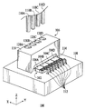
図1及び図2によれば、本発明の実施例による光学サブアセンブリ(OSA)100が示されている。OSA100は、エッジ放出型レーザ104A、104B、104C及び104Dのアレイ102、及び補助取付け基板108に取付けられた光学転向要素106を含む。光学転向要素106は、図1に示すように、例えば光ファイバ110A、110B、110C及び110Dである光導波路に向けて、横向き方向から垂直方向にエッジ放出型レーザからの出力光を再方向付けするために利用される。ここにおいて横向き方向は、補助取付け基板の上側表面に対して平行な方向として、例えば図1に示すX方向として定義される。ここにおいて垂直方向は、横向き方向に対して垂直な方向として、すなわち図1に示すZ方向として定義される。したがって、OSA100は、垂直放出型レーザを有する従来のOSAと互換性があり、そのような従来のOSAと交換することができる。
Referring to FIGS. 1 and 2, an optical subassembly (OSA) 100 according to an embodiment of the present invention is shown. OSA 100 includes an
OSA100のエッジ放出型レーザ104A、104B、104C及び104Dのアレイ102は、変調された出力光を発生するように構成されており、これらの出力光は、光信号として光ファイバ110A、110B、110C及び110Dを通して伝送される。エッジ放出型レーザのアレイは、4つのエッジ放出型レーザを含むものとして、図1に示されている。したがってエッジ放出型レーザの図示したアレイは、4チャネルレーザアレイである。しかしながらエッジ放出型レーザのアレイは、それよりも少ない又はそれよりも多いエッジ放出型レーザを含んでいてもよい。例としてレーザアレイは、12個のエッジ放出型レーザを含むことができる。本実施例において、アレイ内に含まれるエッジ放出型レーザは、ファブリーペロ・レーザである。しかしながらエッジ放出型レーザは、分布ブラッグ反射器型(DBR)レーザのようなその他のタイプのエッジ放出型レーザであってもよい。エッジ放出型レーザは、電気接続部112を介してレーザに接続された回路(図示せず)によって駆動される。エッジ放出型レーザのアレイは、光学転向要素106に隣接して、例えばシリコンからなる補助取付け部108に取付けられている。別の実施例において、OSA100は、エッジ放出型レーザのアレイの代わりに単一のエッジ放出型レーザを含むことができる。
The
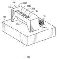
OSA100の光学転向要素106は、出力光を反射しかつ/又は屈折することによって、横向き方向、例えばX方向から垂直方向、すなわちZ方向に、エッジ放出型レーザ104A、104B、104C及び104Dの出力光を再方向付けするように構成されている。したがって光学転向要素は、それぞれのエッジ放出型レーザからの出力光の光軸をほぼ90度だけ転向することができる。加えて光学転向要素は、エッジ放出型レーザからの出力光がそれぞれの光ファイバ110A、110B、110C及び110Dに適切に伝送されるように、それぞれのエッジ放出型レーザからの出力光を集束するように構成されている。光学転向要素は、受信表面114(図1に示す)、反射表面116(図2に示す)及び集束表面118(図1及び図2に示す)を含む。受信表面は、エッジ放出型レーザからの出力光が光学転向要素に伝送される表面である。後に説明するように、受信表面は、出力光が光学転向要素に伝送されるとき、出力光を屈折するような角度をなしていることができる。反射表面は、出力光を光ファイバに向けて反射するようにミラーとして動作する。集束表面は、反射された出力光が光学転向要素から放出される表面である。
The
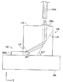
図3に示すように、光学転向要素106の受信及び反射表面114及び116は、X軸に関して角度をなしている。図3は、エッジ放出型レーザ104A、光学転向要素106、補助取付け部108及び光ファイバ110Aに沿ったOSA100の横断面図を示している。受信及び反射表面は、図3に示すように、エッジ放出型レーザ104A、104B、104C及び104Dからのそれぞれの出力光が受信表面によって屈折され、その後、反射表面からそれぞれの光ファイバ110A、110B、110C及び110Dに向かって反射されるように角度をなしている。光学転向要素106は、その受信表面がエッジ放出型レーザ104A、104B、104C及び104Dの光放出エッジにきわめて近接しているように、補助取付け部108に取付けられている。
As shown in FIG. 3, the receiving and reflecting
光学転向要素106の集束表面118は、X軸に対して実質的に平行である。前記のように、集束表面は、反射された出力光が要素から光ファイバに向かって放出される表面である。集束表面は、レンズ120A、120B、120C及び120Dを含み、これらのレンズは、集束表面上に形成されている。したがってレンズは、構造上光学転向要素内に一体化されている。光学転向要素のこれらのレンズは、対応するエッジ放出型レーザ104A、104B、104C及び104Dからの出力光を別々に操作し、これらの出力光は、反射表面116によってそれぞれの光ファイバ110A、110B、110C及び110Dの露出した端部に反射されている。レンズの表面は、エッチングした又は鋳型の屈折又は回折表面として製造することができる。レンズは、光学転向要素から放出された出力光が集束、平行、又は発散して伝搬するように設計することができる。レンズは、1つ又は複数の出力光がレンズから軸を外れて伝搬するように設計することもできる。本実施例において、レンズのピッチは、0.25mmである。しかしながらレンズのピッチは、それよりも短くても長くてもよい。図1及び図2に示すように、光学転向要素は4つのレンズを含み、これらのレンズは、アレイ102の4つのエッジ放出型レーザに対応している。したがって光学転向要素内に含まれるレンズの数は、OSA100内に利用されているエッジ放出型レーザの数に依存している。レンズは屈折及び反射表面とともに、すなわち受信及び反射表面114及び116とともに、光学転向要素に形成されるので、OSA100は、出力光を垂直に放出することができるエッジ放出型レーザを有するある種の従来のOSAの場合のように、3つの部品(レーザ、ミラー構造及びレンズ)ではなく、2つの部品(レーザアレイ102及び光学転向要素106)の位置合わせだけしか必要としない。
The focusing
本実施例において、光学転向要素106はシリコンから製造される。しかしながら光学転向要素は、射出成形プラスチック、プレスガラス、サファイア、III−V材料、又はII−VI材料のようなその他の類似した透明な材料から作ることができる。シリコンから製造することに加えて、光学転向要素は、受信及び反射表面114及び116が、図3に示すように、それぞれX軸からほぼ49.5及び59.9度の角度をなすように製造されている。したがって受信表面及び補助取付け部108の上側表面は、49.5度の角度をなしている。同様に反射表面及び補助取付け部の上側表面は、59.9度の角度をなしている。加えて受信表面及び反射表面は、70.6度の角度をなしている。このような受信及び反射表面を有する光学転向要素は、シリコンウエーハの湿式エッチングによって製造することができ、その間にエッチング液は、角度をなす受信及び反射表面を形成するようにウエーハの部分を除去するために、シリコンウエーハの表面に選択的に加えることができる。シリコンウエーハの結晶配向のために、70.6度の角度をなす受信及び反射表面は、シリコンウエーハの異方性エッチングによって形成することができる。それ故に本実施例において、光学転向要素の構成は、精密な結晶学的な表面を製造するために、通常のシリコン製造プロセス、すなわち湿式エッチングプロセスを利用することを可能にし、これらの表面は、光学転向要素の受信及び反射表面として使われる。受信及び反射表面が、本実施例においてそれぞれX軸からほぼ49.5及び59.9度の角度をなすとはいえ、これらの表面は、受信された光をレンズ120A、120B、120C及び120Dに向かって屈折しかつ反射するために、種々の角度に配向することができる。しかしながら受信及び反射表面は、シリコン湿式エッチングプロセスの利点を取得するために、ほぼ70.6度である角度を形成するようにする必要がある。
In this embodiment, the
動作において、電気制御信号は、1つ又は複数のレーザを活性化するために、電気接続部112を介してアレイ102のエッジ放出型レーザ104A、104B、104C及び104Dに選択的に加えられる。活性化されたそれぞれのエッジ放出型レーザは、その後、その光放出エッジから光学転向要素106の受信表面114に向かって横向き方向に沿って出力光を放出する。出力光は、受信表面を通って光学転向要素内に、要素の反射表面116に向けて進行する。本実施例において、出力光は、受信表面の角度のため、受信表面によって屈折させられる。その後、出力光は、出力光の光軸が当初の横向き方向から垂直方向に要素の集束表面118に向かって再方向付けされるように、反射表面から反射される。したがって出力光は、光学転向要素の受信及び反射表面によってほぼ90度だけ転向させられる。
In operation, an electrical control signal is selectively applied to the
その後、反射した出力光は、光学転向要素106の集束表面118におけるレンズ120A、120B、120C及び120Dの1つを通って進行し、これらのレンズは、出力光が生じるエッジ放出型レーザ104A、104B、104C及び104Dに対応している。したがって出力光は、レンズを通って、レンズ及び対応するエッジ放出型レーザに位置合わせされている光ファイバ110A、110B、110C及び110Dのうちの1つに向かって、光学転向要素から放出される。レンズは、出力光を、この光が効率的に光ファイバ内に伝送されるように集束する。このようにして、それぞれの活性化されたエッジ放出型レーザからの出力光は、そのエッジ放出型レーザに位置合わせされた光ファイバ内に伝送される。
The reflected output light then travels through one of the
OSA100の光学転向要素106が、光線追跡解析を用いて解析された。その結果は、光学転向要素が、適切な反射防止コーティングにより、著しく効率的であり得ることを示した。光線追跡解析は、エッジ放出型レーザ104A、104B、104C及び104Dから光ファイバ110A、110B、110C及び110Dまで、95パーセントを超える総合光学効率を示した。光学効率は、光ファイバ内への損失又は回折非効率性のための損失を含まない。
1つの実施例によるエッジ放出型レーザからの出力光を光導波路に結合する方法を、図4を引用して説明する。ステップ402において、出力光は、出力光がレーザのエッジから当初の方向に放出されるように、エッジ放出型レーザにおいて発生される。次にステップ404において、出力光は、光学転向要素の受信表面を通って光学転向要素内に伝送される。ステップ406において、出力光は、当初の方向から、当初の方向に対してほぼ垂直をなすことができる変更された方向に再方向付けされる。本実施例において、出力光は、光学転向要素の2つの表面を利用して、出力光を屈折しかつ反射することの両方によって再方向付けされる。次にステップ408において、再方向付けされた出力光は、光学転向要素から光学転向要素の集束表面を通って、光ファイバでもよい光導波路に向かって放出される。ステップ408の間、再方向付けされた出力光はまた、集束表面上に形成されたレンズによって光導波路内に光学的に操作される。別の実施例において、追加的なエッジ放出型レーザからの追加的な出力光は、同じ光学転向要素を利用して同様に追加的な光導波路に結合することができる。これらの実施例において、光学転向要素は、光学転向要素から放出される追加的な出力光を光学的に操作するために、集束表面上に形成された追加的なレンズを含む。
A method of coupling output light from an edge emitting laser to an optical waveguide according to one embodiment will be described with reference to FIG. In
本発明の特定の実施例を説明しかつ図解したとはいえ、本発明はこのように説明されかつ図解された部品の特定の形成又は配列に制限されるものではない。本発明の権利範囲は、これに添付した特許請求の範囲及びそれらの均等物によって定義されるものである。 Although particular embodiments of the present invention have been described and illustrated, it is not intended that the invention be limited to the particular forms or arrangements of components thus described and illustrated. It is intended that the scope of the invention be defined by the Claims appended hereto and their equivalents.
100:OSA
104A、104B、104C、104D:光源
106:光学転向要素
110A、110B、110C、110D:導波路
120A、120B、120C、120D:レンズ
100: OSA
104A, 104B, 104C, 104D: light source 106: optical turning
Claims (10)
前記出力光が光学要素内に伝送されるように前記光源からの前記出力光を受信するための第1の表面と、前記出力光を当初の方向から前記導波路に向かう変更された方向に再方向付けするように、前記出力光を内部反射するための第2の表面と、前記出力光を前記導波路に伝送するように、前記変更された方向に沿って伝搬する前記出力光を光学的に操作するためのレンズが形成された第3の表面と、を有する光学要素を備えている装置。 An apparatus for coupling output light from a light source to a waveguide,
A first surface for receiving the output light from the light source such that the output light is transmitted into the optical element; and re-directing the output light from an original direction to a modified direction toward the waveguide. A second surface for internally reflecting the output light so as to direct the light; and optically coupling the output light propagating along the modified direction to transmit the output light to the waveguide. And a third surface having a lens formed thereon for operation.
当初の方向に沿って伝搬する光源からの出力光を光学要素内に伝送するステップと、
前記光学要素内において前記当初の方向から変更された方向へと前記出力光を再方向付けするステップと、
前記変更された方向に沿って伝搬する前記出力光を前記光学要素から前記導波路に向けて放出するステップであって、前記導波路内へ前記出力光を光学的に操作することを含む、ステップと、
を含む方法。 A method of coupling output light from a light source to a waveguide,
Transmitting the output light from the light source propagating along the original direction into the optical element;
Redirecting the output light within the optical element to a direction changed from the original direction;
Emitting the output light propagating along the altered direction from the optical element toward the waveguide, comprising optically manipulating the output light into the waveguide. When,
A method that includes
10. The method of claim 6, 7, 8, or 9 wherein optically manipulating the output light comprises optically manipulating the output light using a lens formed on a surface of the optical element. The described method.
Applications Claiming Priority (1)
| Application Number | Priority Date | Filing Date | Title |
|---|---|---|---|
| US10/319,218 US6921214B2 (en) | 2002-12-12 | 2002-12-12 | Optical apparatus and method for coupling output light from a light source to an optical waveguide |
Publications (2)
| Publication Number | Publication Date |
|---|---|
| JP2004191989A true JP2004191989A (en) | 2004-07-08 |
| JP2004191989A5 JP2004191989A5 (en) | 2007-02-01 |
Family
ID=30443962
Family Applications (1)
| Application Number | Title | Priority Date | Filing Date |
|---|---|---|---|
| JP2003411216A Withdrawn JP2004191989A (en) | 2002-12-12 | 2003-12-10 | Optical device and method for coupling output light from light source to optical waveguide |
Country Status (4)
| Country | Link |
|---|---|
| US (1) | US6921214B2 (en) |
| JP (1) | JP2004191989A (en) |
| DE (1) | DE10349608B4 (en) |
| GB (1) | GB2397393B (en) |
Cited By (2)
| Publication number | Priority date | Publication date | Assignee | Title |
|---|---|---|---|---|
| WO2014136287A1 (en) * | 2013-03-07 | 2014-09-12 | オリンパス株式会社 | Coupling optical system |
| US10545286B2 (en) | 2015-12-28 | 2020-01-28 | Huawei Technologies Co., Ltd. | Housing for packaging optical transmitter module and optical transmitter module |
Families Citing this family (19)
| Publication number | Priority date | Publication date | Assignee | Title |
|---|---|---|---|---|
| DE10314494B3 (en) * | 2003-03-27 | 2004-11-18 | Infineon Technologies Ag | Electro-optical module for optical communications has lenses having relatively angled optical axes respectively aligned with common waveguide and associated electro-optical components |
| JP4022498B2 (en) * | 2003-04-18 | 2007-12-19 | インターナショナル・ビジネス・マシーンズ・コーポレーション | OPTICAL LINK MODULE, OPTICAL CONNECTION METHOD, INFORMATION PROCESSING DEVICE INCLUDING THE OPTICAL LINK MODULE, SIGNAL TRANSFER METHOD, PRISM, AND MANUFACTURING METHOD THEREOF |
| US7099536B1 (en) * | 2003-12-08 | 2006-08-29 | National Semiconductor Corporation | Single lens system integrating both transmissive and reflective surfaces for light focusing to an optical fiber and light reflection back to a monitor photodetector |
| TWI242938B (en) * | 2004-02-20 | 2005-11-01 | Ind Tech Res Inst | Parallel optical subassembly module structure |
| US7543999B2 (en) | 2004-09-13 | 2009-06-09 | Hymite A/S | Optical module hermetically packaged in micro-machined structures |
| JP4559952B2 (en) * | 2004-11-04 | 2010-10-13 | ホシデン株式会社 | Optical coupling member for optical communication connector, optical connector using the same, and optical connector assembling method |
| US20060110110A1 (en) * | 2004-11-22 | 2006-05-25 | Yi Robert H | Optical turn system for optoelectronic modules |
| JP4690963B2 (en) * | 2006-08-09 | 2011-06-01 | 株式会社日立製作所 | Manufacturing method of multi-channel optical module |
| JP2008257094A (en) * | 2007-04-09 | 2008-10-23 | Hitachi Cable Ltd | Optical transmission module and optical patch cable |
| US8000358B2 (en) * | 2009-04-20 | 2011-08-16 | Emcore Corporation | Power monitoring system for a parallel optical transmitter |
| US9134489B2 (en) | 2009-11-11 | 2015-09-15 | Samtec, Inc. | Optical engine for active optical cable |
| US20110206379A1 (en) * | 2010-02-25 | 2011-08-25 | International Business Machines Corporation | Opto-electronic module with improved low power, high speed electrical signal integrity |
| US8876408B2 (en) * | 2010-04-23 | 2014-11-04 | Ruprecht-Karls-Universität Heidelberg | Optical connectors and a method of production thereof |
| US9151918B2 (en) * | 2010-08-26 | 2015-10-06 | Vi Systems Gmbh | Opto-electronic assembly for parallel high speed transmission |
| TWI553364B (en) * | 2011-12-19 | 2016-10-11 | 鴻海精密工業股份有限公司 | Photoelectric converter |
| US9435963B2 (en) * | 2012-03-30 | 2016-09-06 | Corning Cable Systems Llc | Misalignment-tolerant total-internal-reflection fiber optic interface modules and assemblies with high coupling efficiency |
| US10146009B2 (en) * | 2013-07-04 | 2018-12-04 | Mellanox Technologies, Ltd. | Silicon photonics connector |
| US9261660B2 (en) * | 2014-07-09 | 2016-02-16 | Hon Hai Precision Industry Co., Ltd. | Optical coupling lens, optical communiction device, and method for assembling same |
| CN107346053A (en) * | 2016-05-08 | 2017-11-14 | 迈络思科技有限公司 | Silicon photon connector |
Family Cites Families (34)
| Publication number | Priority date | Publication date | Assignee | Title |
|---|---|---|---|---|
| US4163953A (en) * | 1977-07-07 | 1979-08-07 | Northern Telecom Limited | Double heterostructure laser for direct coupling to an optical fiber |
| US4699453A (en) * | 1982-11-24 | 1987-10-13 | Magnetic Controls Company | Monolithic fiber optic coupler having total internal reflecting surface |
| JPS60124983A (en) | 1983-12-12 | 1985-07-04 | Nec Corp | Semiconductor laser |
| US4701010A (en) * | 1984-08-30 | 1987-10-20 | Adc Fiber Optics Corporation | Unitary body optical coupler |
| DE3925128A1 (en) * | 1989-07-28 | 1991-01-31 | Hirschmann Richard Gmbh Co | OPTOELECTRIC TRANSMITTER AND RECEIVER |
| US5122652A (en) * | 1989-09-29 | 1992-06-16 | Siemens Aktiengesellschaft | Means for deflecting and focusing a light beam with silicon optical members |
| JPH04289531A (en) * | 1990-05-21 | 1992-10-14 | Ricoh Co Ltd | Optical information recording and reproducing device and prism coupler |
| EP0613032B1 (en) | 1993-02-23 | 1999-01-20 | The Whitaker Corporation | Fiber optic coupling devices |
| DE4416563C1 (en) * | 1994-05-11 | 1995-07-20 | Ant Nachrichtentech | Coupler for connecting opto-electronic device to waveguide |
| DE4440976A1 (en) * | 1994-11-17 | 1996-05-23 | Ant Nachrichtentech | Optical transmitter and receiver with a surface emitting laser |
| JP3828179B2 (en) * | 1995-05-12 | 2006-10-04 | 富士通株式会社 | Semiconductor photodetection device and manufacturing method thereof |
| DE19519059A1 (en) | 1995-05-24 | 1996-11-28 | Bosch Gmbh Robert | Arrangement for coupling a laser |
| US5742720A (en) * | 1995-08-30 | 1998-04-21 | Matsushita Electric Industrial Co., Ltd. | Optical coupling module and method for producing the same |
| JP3456809B2 (en) * | 1995-10-30 | 2003-10-14 | シャープ株式会社 | Optical waveguide device, method of coupling to optical waveguide device, and optical pickup device |
| JPH1010373A (en) * | 1996-06-21 | 1998-01-16 | Toshiba Corp | Receptacle type optical transmitter-receiver and production therefor |
| DE19640423C1 (en) * | 1996-09-30 | 1998-03-26 | Siemens Ag | Optoelectronic module for bidirectional optical data transmission |
| US5886370A (en) * | 1997-05-29 | 1999-03-23 | Xerox Corporation | Edge-emitting semiconductor lasers |
| JP3064969B2 (en) * | 1997-07-03 | 2000-07-12 | 日本電気株式会社 | Light receiving module and manufacturing method thereof |
| JPH11128796A (en) * | 1997-10-30 | 1999-05-18 | Itw Dynatec Kk | Applicator for reaction type hot melt adhesive |
| US6115521A (en) * | 1998-05-07 | 2000-09-05 | Trw Inc. | Fiber/waveguide-mirror-lens alignment device |
| DE19823691A1 (en) * | 1998-05-27 | 1999-12-02 | Siemens Ag | Housing arrangement for laser module |
| US6385374B2 (en) * | 1999-01-06 | 2002-05-07 | Infineon Technologies Ag | Multichannel electro-optical assembly |
| DE19959781C2 (en) * | 1999-12-07 | 2003-02-20 | Infineon Technologies Ag | Opto-electronic assembly with integrated imaging system |
| JP2001174671A (en) * | 1999-12-16 | 2001-06-29 | Japan Aviation Electronics Industry Ltd | Optical element module |
| US6328484B1 (en) * | 2000-03-02 | 2001-12-11 | Agilent Technologies, Inc. | Fiber optic lens system for coupling fibers to surface mounted devices |
| US6454470B1 (en) * | 2000-08-31 | 2002-09-24 | Stratos Lightwave, Inc. | Optoelectronic interconnect module |
| AU2002248276B2 (en) * | 2000-10-31 | 2006-07-06 | Viasystems Group, Inc. | Fiber optic circuit board connector |
| IL155688A0 (en) | 2000-11-01 | 2003-11-23 | Intel Corp | System and method for collimating and redirecting beams |
| US6516111B1 (en) * | 2000-11-15 | 2003-02-04 | Optical Switch Corporation | Cascaded integrated fiber array optical switch and method of operation |
| US6668113B2 (en) * | 2001-09-19 | 2003-12-23 | Finisar Corporation | Compact optical assembly for optoelectronic transceivers |
| CN100368842C (en) | 2002-03-14 | 2008-02-13 | 新科实业有限公司 | Integrated platform for passive optical alignment of semiconductor device and optical fiber |
| US20040042705A1 (en) * | 2002-08-27 | 2004-03-04 | Uchida Toshi K. | Embedded optical coupling in circuit boards |
| JP2004240220A (en) * | 2003-02-06 | 2004-08-26 | Seiko Epson Corp | Optical module, its manufacturing method, hybrid integrated circuit, hybrid circuit board, electronic appliance, photoelectric hybrid device and its manufacturing method |
| US6752379B1 (en) * | 2003-05-16 | 2004-06-22 | Richard L. Wall | Adjustable toilet dolly |
-
2002
- 2002-12-12 US US10/319,218 patent/US6921214B2/en not_active Expired - Lifetime
-
2003
- 2003-10-24 DE DE10349608A patent/DE10349608B4/en not_active Expired - Fee Related
- 2003-12-10 JP JP2003411216A patent/JP2004191989A/en not_active Withdrawn
- 2003-12-11 GB GB0328750A patent/GB2397393B/en not_active Expired - Fee Related
Cited By (2)
| Publication number | Priority date | Publication date | Assignee | Title |
|---|---|---|---|---|
| WO2014136287A1 (en) * | 2013-03-07 | 2014-09-12 | オリンパス株式会社 | Coupling optical system |
| US10545286B2 (en) | 2015-12-28 | 2020-01-28 | Huawei Technologies Co., Ltd. | Housing for packaging optical transmitter module and optical transmitter module |
Also Published As
| Publication number | Publication date |
|---|---|
| GB2397393B (en) | 2007-05-16 |
| DE10349608B4 (en) | 2007-08-09 |
| US20040114881A1 (en) | 2004-06-17 |
| GB0328750D0 (en) | 2004-01-14 |
| GB2397393A (en) | 2004-07-21 |
| DE10349608A1 (en) | 2004-07-08 |
| US6921214B2 (en) | 2005-07-26 |
Similar Documents
| Publication | Publication Date | Title |
|---|---|---|
| US6921214B2 (en) | Optical apparatus and method for coupling output light from a light source to an optical waveguide | |
| US6987906B2 (en) | Optical connection device | |
| US9869829B2 (en) | Optical interposer for waveguides | |
| US8611716B2 (en) | Channeled substrates for integrated optical devices employing optical fibers | |
| KR101443562B1 (en) | Optical connector | |
| KR101453136B1 (en) | Optical splitter device | |
| US9244234B2 (en) | Optical receptacle and optical module | |
| US9077450B2 (en) | Wavelength division multiplexing with multi-core fiber | |
| US9036955B2 (en) | Optical interposer | |
| JP2004029798A (en) | Alignment device | |
| CN108387978B (en) | Optical coupling system and optical coupling method | |
| US10048458B2 (en) | Optical module | |
| CN113917625A (en) | Optical module and method for manufacturing optical module | |
| US6381386B1 (en) | V-shaped optical coupling structure | |
| US7212711B2 (en) | Fiber optic transceiver module and electronic equipment | |
| US20180335575A1 (en) | Microfabricated fiber optic platform | |
| JP2015121670A (en) | Lens block and optical communication module | |
| JPH10170765A (en) | Optical waveguide | |
| JP2006201499A (en) | Optical communication module | |
| KR19990013585A (en) | Optical communication device and method | |
| US20220187551A1 (en) | Optical receptacle, optical module, and method for manufacturing optical module | |
| US20040190832A1 (en) | Optical coupling unit | |
| JP2000081546A (en) | Optical module | |
| TWM606271U (en) | End structure of optical transmission member | |
| TW202215087A (en) | Terminal structure of optical transmission member capable of facilitating the assembly and manufacturing and reducing the size of the entire member |
Legal Events
| Date | Code | Title | Description |
|---|---|---|---|
| A521 | Written amendment |
Free format text: JAPANESE INTERMEDIATE CODE: A523 Effective date: 20061206 |
|
| A621 | Written request for application examination |
Free format text: JAPANESE INTERMEDIATE CODE: A621 Effective date: 20061206 |
|
| A711 | Notification of change in applicant |
Free format text: JAPANESE INTERMEDIATE CODE: A711 Effective date: 20070320 |
|
| A521 | Written amendment |
Free format text: JAPANESE INTERMEDIATE CODE: A821 Effective date: 20070409 |
|
| RD02 | Notification of acceptance of power of attorney |
Free format text: JAPANESE INTERMEDIATE CODE: A7422 Effective date: 20070409 |
|
| A761 | Written withdrawal of application |
Free format text: JAPANESE INTERMEDIATE CODE: A761 Effective date: 20070801 |