JP2004170955A - Image forming apparatus, cartridge, image forming system and memory medium for cartridge - Google Patents
Image forming apparatus, cartridge, image forming system and memory medium for cartridge Download PDFInfo
- Publication number
- JP2004170955A JP2004170955A JP2003370552A JP2003370552A JP2004170955A JP 2004170955 A JP2004170955 A JP 2004170955A JP 2003370552 A JP2003370552 A JP 2003370552A JP 2003370552 A JP2003370552 A JP 2003370552A JP 2004170955 A JP2004170955 A JP 2004170955A
- Authority
- JP
- Japan
- Prior art keywords
- image forming
- cartridge
- image
- memory medium
- information
- Prior art date
- Legal status (The legal status is an assumption and is not a legal conclusion. Google has not performed a legal analysis and makes no representation as to the accuracy of the status listed.)
- Pending
Links
Images


Classifications
-
- G—PHYSICS
- G03—PHOTOGRAPHY; CINEMATOGRAPHY; ANALOGOUS TECHNIQUES USING WAVES OTHER THAN OPTICAL WAVES; ELECTROGRAPHY; HOLOGRAPHY
- G03G—ELECTROGRAPHY; ELECTROPHOTOGRAPHY; MAGNETOGRAPHY
- G03G15/00—Apparatus for electrographic processes using a charge pattern
- G03G15/06—Apparatus for electrographic processes using a charge pattern for developing
- G03G15/08—Apparatus for electrographic processes using a charge pattern for developing using a solid developer, e.g. powder developer
-
- G—PHYSICS
- G03—PHOTOGRAPHY; CINEMATOGRAPHY; ANALOGOUS TECHNIQUES USING WAVES OTHER THAN OPTICAL WAVES; ELECTROGRAPHY; HOLOGRAPHY
- G03G—ELECTROGRAPHY; ELECTROPHOTOGRAPHY; MAGNETOGRAPHY
- G03G21/00—Arrangements not provided for by groups G03G13/00 - G03G19/00, e.g. cleaning, elimination of residual charge
- G03G21/16—Mechanical means for facilitating the maintenance of the apparatus, e.g. modular arrangements
- G03G21/18—Mechanical means for facilitating the maintenance of the apparatus, e.g. modular arrangements using a processing cartridge, whereby the process cartridge comprises at least two image processing means in a single unit
- G03G21/1875—Mechanical means for facilitating the maintenance of the apparatus, e.g. modular arrangements using a processing cartridge, whereby the process cartridge comprises at least two image processing means in a single unit provided with identifying means or means for storing process- or use parameters, e.g. lifetime of the cartridge
- G03G21/1878—Electronically readable memory
- G03G21/1889—Electronically readable memory for auto-setting of process parameters, lifetime, usage
-
- G—PHYSICS
- G03—PHOTOGRAPHY; CINEMATOGRAPHY; ANALOGOUS TECHNIQUES USING WAVES OTHER THAN OPTICAL WAVES; ELECTROGRAPHY; HOLOGRAPHY
- G03G—ELECTROGRAPHY; ELECTROPHOTOGRAPHY; MAGNETOGRAPHY
- G03G15/00—Apparatus for electrographic processes using a charge pattern
- G03G15/50—Machine control of apparatus for electrographic processes using a charge pattern, e.g. regulating differents parts of the machine, multimode copiers, microprocessor control
-
- G—PHYSICS
- G03—PHOTOGRAPHY; CINEMATOGRAPHY; ANALOGOUS TECHNIQUES USING WAVES OTHER THAN OPTICAL WAVES; ELECTROGRAPHY; HOLOGRAPHY
- G03G—ELECTROGRAPHY; ELECTROPHOTOGRAPHY; MAGNETOGRAPHY
- G03G2221/00—Processes not provided for by group G03G2215/00, e.g. cleaning or residual charge elimination
- G03G2221/16—Mechanical means for facilitating the maintenance of the apparatus, e.g. modular arrangements and complete machine concepts
- G03G2221/18—Cartridge systems
- G03G2221/1823—Cartridges having electronically readable memory
Abstract
Description
本発明は、レーザービームプリンタ、複写機、ファクシミリなどの電子写真方式を用いた画像形成装置と、その画像形成装置に装着するプロセスカートリッジ、更には、プロセスカートリッジを用いて記録媒体に画像を形成する画像形成システム、プロセスカートリッジに搭載されたプロセスカートリッジ用メモリ媒体に関するものである。 The present invention relates to an image forming apparatus using an electrophotographic method such as a laser beam printer, a copying machine, and a facsimile, a process cartridge mounted on the image forming apparatus, and further, forms an image on a recording medium using the process cartridge. The present invention relates to an image forming system and a memory medium for a process cartridge mounted on a process cartridge.
複写機やレーザービームプリンタ等の電子写真方式の画像形成装置は、画像情報に対応した光を電子写真用の感光体に照射して潜像を形成し、この潜像に現像手段で記録材料である現像剤(トナー)を供給して顕像化し、更に感光体から記録紙等の記録媒体へと画像を転写することで記録紙上に画像を形成している。 2. Description of the Related Art Electrophotographic image forming apparatuses such as copiers and laser beam printers form a latent image by irradiating light corresponding to image information to a photoconductor for electrophotography, and develop the latent image with a recording material by a developing unit. An image is formed on a recording paper by supplying a certain developer (toner) to visualize the image, and further transferring the image from a photoconductor to a recording medium such as a recording paper.
このような画像形成装置において、感光体、トナーなどの消耗品の交換メンテナンスの簡便性を図る目的で、トナー収納部や現像手段、感光体、帯電手段、廃トナー容器を含むクリーニング手段などを、プロセスカートリッジとして一体化し、画像形成装置に対し着脱可能に構成されているものも多い。また、カラー画像形成装置のように、複数色の現像手段を持ち各現像手段の消耗具合が違う場合や、感光体ドラムの消耗具合と現像手段の消耗具合が違う場合などで、各色現像カートリッジ、クリーニング手段と、感光体ドラムとを一体化した感光体カートリッジなど個別にプロセスカートリッジ化されているものもある。 In such an image forming apparatus, for the purpose of facilitating replacement maintenance of consumables such as a photoconductor and toner, a toner storage unit and a developing unit, a photoconductor, a charging unit, a cleaning unit including a waste toner container, and the like are provided. Many are integrated as a process cartridge and configured to be detachable from the image forming apparatus. Further, when a developing device of a plurality of colors is used and a developing condition of each developing device is different, as in a color image forming apparatus, or when a developing condition of a photosensitive drum is different from a developing condition of a developing device, a developing cartridge of each color is used. Some photoconductor cartridges are integrated into a process cartridge, such as a photoconductor cartridge in which the cleaning unit and the photoconductor drum are integrated.
ここで、プロセスカートリッジとは、帯電手段、現像手段及びクリーニング手段の少なくとも一つと、電子写真用の感光体とを一体的にカートリッジ化し、このカートリッジを電子写真方式の画像形成装置本体に対して着脱可能とするものであるか、あるいは、少なくとも現像手段と電子写真用の感光体とを一体的にカートリッジ化し、このカートリッジを電子写真方式の画像形成装置本体に対して着脱可能とするものをいう。 Here, the process cartridge is a cartridge in which at least one of a charging unit, a developing unit, and a cleaning unit and a photoconductor for electrophotography are integrally formed into a cartridge, and this cartridge is attached to and detached from an electrophotographic image forming apparatus main body. This means that the developing means and at least the electrophotographic photosensitive member are integrally formed into a cartridge, and this cartridge is detachable from the main body of the electrophotographic image forming apparatus.
また、これらカートリッジに記憶手段(メモリ)を搭載しカートリッジ情報を管理するものもある。メモリ内にカートリッジ使用量を記憶して種々のプロセス条件を変更するものもある(例えば、特許文献1参照。)。例えば、帯電電流値を切り換えたり、露光量を調節する。これらは、カートリッジが異なっているにも拘らず、使用された量が同じであれば、同一の制御がなされる。 There is also a type in which storage means (memory) is mounted on these cartridges to manage cartridge information. In some cases, various process conditions are changed by storing a cartridge usage amount in a memory (for example, see Patent Document 1). For example, the charging current value is switched or the exposure amount is adjusted. In these cases, the same control is performed if the used amount is the same, although the cartridges are different.
また、カートリッジごとの特性に応じて、メモリ媒体に記憶された情報を基に帯電電圧値と現像電圧値の切り換えを行い、個体差を吸収して耐久を通じて画像を安定させているものもある(例えば、特許文献2及び特許文献3参照。)。
しかしながら、プロセススピードやスループットなどの複数の動作条件が備わった画像形成システムの場合、プロセスカートリッジの使用量が同じであっても、使用量の画像に対する影響がプロセススピードやスループットなどによって異なることから、複数の動作条件で全く同じ品質で画像を出力することはできなかった。 However, in the case of an image forming system having a plurality of operating conditions such as a process speed and a throughput, even if the amount of use of the process cartridge is the same, the influence of the amount of use on the image differs depending on the process speed and the throughput. It was not possible to output an image with exactly the same quality under a plurality of operating conditions.
本発明の目的は、上記課題を解決するためのものであり、
安定した画像を形成可能とする画像形成装置及びカートリッジ、画像形成システム、カートリッジ用メモリ媒体を提供することである。
An object of the present invention is to solve the above problems,
An object of the present invention is to provide an image forming apparatus, a cartridge, an image forming system, and a memory medium for a cartridge that can form a stable image.
また、本発明の他の目的は、
複数の画像形成速度を有する画像形成装置において、画像形成速度の違いによって生じる画像のばらつきを補正して安定した画像を形成可能とする画像形成装置及びカートリッジ、画像形成システム、カートリッジ用メモリ媒体を提供することである。
Another object of the present invention is to
Provided are an image forming apparatus, a cartridge, an image forming system, and a memory medium for a cartridge that can form a stable image by correcting image variations caused by differences in image forming speeds in an image forming apparatus having a plurality of image forming speeds. It is to be.
また、本発明の他の目的は、メモリ内にカートリッジが使用されることに伴って累積される使用量情報と、使用量と比較される閾値情報と、使用量が閾値に達したときに設定されるべきプロセス条件に係わる情報を、装置の動作条件に対応して複数記憶することで、使用量の異なったカートリッジが動作条件の違いによって生じる画像のばらつきを補正し、安定した画像を提供することのできるプロセスカートリッジ用メモリ媒体、プロセスカートリッジ、プロセスカートリッジが着脱自在とされる画像形成装置及び画像形成システムを提供することである。 Further, another object of the present invention is to set usage information accumulated when the cartridge is used in the memory, threshold information to be compared with the usage, and setting when the usage reaches the threshold. By storing a plurality of pieces of information relating to process conditions to be performed in accordance with the operating conditions of the apparatus, cartridges having different usage amounts correct image variations caused by differences in operating conditions, and provide stable images. It is an object of the present invention to provide a process cartridge memory medium, a process cartridge, and an image forming apparatus and an image forming system in which the process cartridge is detachable.
本発明の画像形成装置は、
カートリッジが装着可能であり、複数の画像形成速度で画像形成可能な画像形成装置であって、前記カートリッジは、前記画像形成速度に対応した前記プロセス要素の画像形成条件に係わる情報を記憶するための第1の記憶領域を有するメモリ媒体を有し、
画像形成装置本体は、前記画像形成条件を設定する制御ユニットを有し、
前記制御ユニットは、前記画像形成速度に対応した前記プロセス要素の画像形成条件に係わる情報に基づいて、前記画像形成速度に応じた画像形成条件を設定することを特徴とする。
The image forming apparatus of the present invention includes:
An image forming apparatus in which a cartridge is mountable and capable of forming an image at a plurality of image forming speeds, wherein the cartridge stores information relating to image forming conditions of the process element corresponding to the image forming speed. A memory medium having a first storage area;
The image forming apparatus main body has a control unit for setting the image forming conditions,
The control unit sets an image forming condition according to the image forming speed based on information about an image forming condition of the process element corresponding to the image forming speed.
また、本発明のカートリッジは、
複数の画像形成条件で画像形成可能な画像形成装置本体に着脱可能であって、画像形成を行うためのプロセス要素の一部と、メモリ媒体が備えられたカートリッジにおいて、
前記メモリ媒体は、前記画像形成速度に対応した前記プロセス要素の画像形成条件に係わる情報を記憶するための第1の記憶領域を有することを特徴とする。
Further, the cartridge of the present invention
In a cartridge which is detachable from an image forming apparatus main body capable of forming an image under a plurality of image forming conditions and is provided with a part of a process element for forming an image and a memory medium,
The memory medium has a first storage area for storing information related to image forming conditions of the process element corresponding to the image forming speed.
また、本発明のメモリ媒体は、
複数の画像形成条件で画像形成可能な画像形成装置本体に着脱可能であって、画像形成を行うためのプロセス要素の一部を有するカートリッジに搭載されるメモリ媒体において、
前記メモリ媒体は、前記画像形成速度に対応した前記プロセス要素の画像形成条件に係わる情報を記憶するための第1の記憶領域を有することを特徴とする。
Further, the memory medium of the present invention includes:
In a memory medium which is detachable from an image forming apparatus main body capable of forming an image under a plurality of image forming conditions and is mounted on a cartridge having a part of a process element for performing image formation,
The memory medium has a first storage area for storing information related to image forming conditions of the process element corresponding to the image forming speed.
また、本発明の画像形成システムは、
装置本体とカートリッジを有し、複数の画像形成条件で画像形成可能な画像形成装置の画像形成システムにおいて、
前記画像形成装置は、画像形成を行うためのプロセス要素の一部を有し、
前記システムは、前記カートリッジに搭載されるメモリ媒体を有し、
前記メモリ媒体は、前記画像形成速度に対応した前記プロセス要素の画像形成条件に係わる情報を記憶するための第1の記憶領域を有し、
更に、前記画像形成条件を設定する制御ユニットを有し、
前記制御ユニットは、前記画像形成速度に対応した前記プロセス要素の画像形成条件に係わる情報に基づいて、前記画像形成速度に応じた画像形成条件を設定することを特徴とする。
Further, the image forming system of the present invention includes:
In an image forming system of an image forming apparatus having an apparatus main body and a cartridge and capable of forming an image under a plurality of image forming conditions,
The image forming apparatus has a part of a process element for performing image formation,
The system includes a memory medium mounted on the cartridge,
The memory medium has a first storage area for storing information related to an image forming condition of the process element corresponding to the image forming speed,
A control unit for setting the image forming conditions;
The control unit sets an image forming condition according to the image forming speed based on information about an image forming condition of the process element corresponding to the image forming speed.
本発明によれば、画像形成の動作条件の違いによって生じる画像のばらつきを補正でき、安定した画像を提供することが可能となる。 ADVANTAGE OF THE INVENTION According to this invention, the dispersion | variation of the image which arises by the difference of the operation conditions of image formation can be corrected, and it becomes possible to provide a stable image.
以下、本発明に係るプロセスカートリッジ、プロセスカートリッジが着脱自在とされる画像形成装置及び画像形成システム、更には、プロセスカートリッジ用メモリ媒体を図面に則して更に詳しく説明する。 Hereinafter, a process cartridge, an image forming apparatus and an image forming system in which the process cartridge is detachable, and a memory medium for the process cartridge according to the present invention will be described in more detail with reference to the drawings.
実施例1
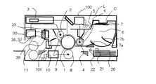
先ず、図2を参照して、本発明に従って構成されるプロセスカートリッジを装着可能な電子写真方式の画像形成装置の実施例について説明する。本実施例の画像形成装置は、ホストコンピューターからの画像情報を受け取り、画像出力するレーザービームプリンタであり、このレーザービームプリンタは、ドラム形状の電子写真感光体、即ち、感光体ドラム、現像剤などの消耗品をプロセスカートリッジとして本体から着脱し交換可能にした画像形成装置である。先ず、図2を参照して本実施例の電子写真画像形成装置及びプロセスカートリッジを説明する。
Example 1
First, an embodiment of an electrophotographic image forming apparatus to which a process cartridge configured according to the present invention can be mounted will be described with reference to FIG. The image forming apparatus of the present embodiment is a laser beam printer that receives image information from a host computer and outputs an image. This laser beam printer is a drum-shaped electrophotographic photosensitive member, that is, a photosensitive drum, a developer, and the like. This is an image forming apparatus in which the above consumables are detachable from the main body as a process cartridge and are replaceable. First, an electrophotographic image forming apparatus and a process cartridge according to the present embodiment will be described with reference to FIG.
本実施例にて、プロセスカートリッジCは、画像形成を行うためのプロセス要素としての、ドラム形状の感光体、即ち、感光体ドラム1と、感光体ドラム1を均一に帯電するための接触帯電ローラ2と、感光体ドラム1に対向配置された現像手段を構成する現像スリーブ4及び現像スリーブ4を回転自在に担持した現像剤Tを収容した現像剤収納容器6と、クリーニング手段を構成するクリーニングブレード9及びクリーニングブレード9により感光体ドラム1から除去された残留トナーを収容する廃トナー容器10と、が一体的に構成されている。このプロセスカートリッジCは、ユーザーによって画像形成装置本体100に設けた装着手段101に対して取り外し可能に装着される。
In the present embodiment, the process cartridge C is a drum-shaped photosensitive member as a process element for forming an image, that is, a
現像手段における現像スリーブ5は、直径20mmの非磁性アルミニウム製スリーブで、表面に導電性粒子を含有する樹脂層でコートしたスリーブである。現像スリーブ4内には図示していないが4極のマグネットロールが配置されている。現像剤収納容器6には、現像ブレード、即ち、現像剤規制部材5が取り付けられている。本実施例で現像剤規制部材5は、JIS硬度65゜程度のウレタンゴムにて作製し、現像スリーブ4に対して当接力が25〜35gf/cm(現像スリーブ4の長手方向についての1cm当たりの当接荷重)となるように当接されている。
The developing
本実施例で、現像剤収納容器6内に収容された現像剤Tは、負帯電性磁性一成分トナー(以降単に「トナー」という。)が用いられる。なお、本実施例で用いられたトナーはポリエステル樹脂が主成分の結着樹脂と、磁性酸化鉄からなっている。また、磁性酸化鉄はそれを基準として、0.1〜2.0質量%のSiと、0.10乃至4.00質量%のZnを有している。このトナーの製造方法としては、原料を混合し、溶融して冷却固化後に、機械式粉砕機にて、温度を調整しつつ、粉体原料の粉砕処理及び表面処理を行う方法を用いた。さらに、粉砕後に重量平均径5.0μmの分級を行って、疎水性シリカ微分体を1.3質量部とチタン酸ストロンチウム1.0質量部を外添混合して調整する。そして、重量平均粒径が5.0〜7.0μmの範囲(主に6μm程度)のものが用いられる。
In this embodiment, the developer T stored in the
現像スリーブ4に印加される現像バイアスは、例えば感光体ドラム1と現像スリーブ4間のギャップが300μm程度であった場合、直流電圧:−550〜−400V、交流電圧:矩形波Vpp1600V、周波数2600Hzを印加する。
For example, when the gap between the
現像剤収納容器、即ち、トナー容器6内にはトナー撹拌手段7a、7bがあり、それぞれ3秒に2回、3秒1回の割合で回転し、トナー容器6内のトナーTをほぐしながら、現像領域にトナーを送り込んでいる。
In the developer accommodating container, that is, the
帯電ローラ2は、芯金の表面に導電弾性体を形成したもので、芯金の両端部を回転自在に保持され、所定の押圧力にて感光体ドラム1の外周面に圧接され、感光体ドラム1の回転に従動回転する。
The charging
帯電ローラ2には画像形成装置本体100内に設けられた高圧電源から芯金を介して、帯電開始電圧の2倍以上のピーク間電圧Vppを有するAC成分VacとDC成分Vdcとの重畳電圧(Vac+Vdc)が帯電ローラ2に印加されて、回転駆動されている感光体ドラム1の外周面がAC印加方式で均一に接触帯電処理される。
A superimposed voltage of an AC component Vac and a DC component Vdc having a peak-to-peak voltage Vpp equal to or more than twice the charging start voltage is applied to the charging
帯電ローラ2に印加される帯電バイアスは、直流電圧:−720〜−520V、交流電圧:正弦波、周波数=2500Hz、実効電流値=1900μAを印加する。また、直流電圧の印加は定電圧制御で行い、交流電圧の印加は定電流値制御で行っている。感光体ドラム1の帯電電位はVd=−700〜−500Vに帯電され、レーザ露光部の電位をVL=−200〜−100Vとし、これによりレーザ露光部(VL部)を反転現像する。
As a charging bias applied to the charging
潜像担持体たる円筒状の感光体ドラム1は、装置本体100に担持された軸を中心として矢印に回転する。本実施例は感光体ドラムの表面移動速度であるプロセススピードを2段階有し、Va=270mm/secまたはVb=135mm/secで回転駆動を行っている。
The cylindrical
感光体ドラム1は帯電ローラ2にその表面を一様に帯電された後、露光装置3により潜像を形成される。感光体ドラム1上に形成された潜像は、現像装置を構成する現像スリーブ4によりトナーTを供給して可視化される。感光体ドラム1と現像スリーブ5の間には、直流バイアスに交流バイアスを重畳したバイアス供給電源(図示せず)が接続されており、適正な現像バイアスを与えるようになっている。
After the surface of the
上述のようにしてトナーTにより可視化された感光体ドラム1上のトナー像は転写ローラ8により記録紙のような記録媒体20に転写される。記録媒体20は給紙ローラ21で給紙され、レジストローラ22により感光体ドラム1上の像と同期がとられて転写ローラ8に送られる。そして、記録媒体20に転写されたトナーTによる可視像は、転写材20とともに定着装置11に搬送され熱若しくは圧力により定着され記録画像となる。一方、転写後に転写されず感光体ドラム1上に残ったトナーTはクリーニングブレード9により除かれ、廃トナー容器10に収容される。その後、感光体ドラム表面は再び帯電ローラ2によって帯電され上述の工程を繰り返す。
The toner image on the
次に、上記プロセスカートリッジに装着されるプロセスカートリッジ用メモリ媒体、即ち、メモリについて説明する。 Next, a process cartridge memory medium mounted on the process cartridge, that is, a memory will be described.
本実施例の場合、カートリッジCは、廃トナー容器10の側面部に、メモリ30と、本体に備えられた読み込み手段36と書き出し手段37に適正な位置で接触して、メモリ30の情報をCPUである制御手段40に伝達する伝達手段35を有している。カートリッジCを画像形成装置本体100に装着した場合は、伝達手段35と画像形成装置本体側の読み込み手段36と書き出し手段37が互いに対向して配置されている。本発明に使用されるメモリ30としては、通常の半導体による電子的なメモリが特に制限無く使用することができる。
In the case of the present embodiment, the cartridge C comes into contact with the side surface of the
これらの読み込み手段36と書き出し手段37と伝達手段35によってメモリ30内の情報の読み出し及び書き込みを行うための制御伝達部38が構成される。メモリ30の容量については、後述するカートリッジCの使用量情報や設定されるべきプロセス条件を特定する情報などの複数個の情報を記憶するのに十分な容量をもつものとする。
The
また、本発明によれば、メモリ30には、カートリッジCが使用された量が書き込まれて記憶される。メモリ30内容の中のカートリッジ使用量は、画像形成装置によって判断できるなら特に制限はない。例えば、各ユニットの回転時間、バイアス印加時間、トナー残量、印字枚数、感光体ドラム1に作像する画像ドット数、感光体ドラム1を露光する際のレーザ発光時間の積算値及び感光体ドラム1の感光層の膜厚、それぞれの使用量の重み付けを行って組み合わせた値などが挙げられる。
Further, according to the present invention, the used amount of the cartridge C is written and stored in the
また、カートリッジCの使用量と比較される閾値情報と、使用量が閾値に達したときに設定されるべきプロセス条件を特定する情報は工場出荷時等であらかじめメモリ内に記憶されるべき情報である。閾値情報はプロセス条件を切り替える、タイミングに関する情報であり、例えば、各ユニットの回転時間、バイアス印加時間、トナー残量、印字枚数、感光体ドラム1に作像する画像ドット数、感光体ドラム1を露光する際のレーザ発光時間の積算値及び感光体ドラム1の感光層の膜厚、それぞれの使用量の重み付けを行って組み合わせた値など、あらかじめ設定された値がプロセス条件を切り換えるタイミングとして使用できる。
The threshold information to be compared with the usage amount of the cartridge C and the information for specifying the process condition to be set when the usage amount reaches the threshold value are information to be stored in a memory in advance at the time of factory shipment or the like. is there. The threshold information is information on timing for switching process conditions. For example, the rotation time of each unit, the bias application time, the remaining amount of toner, the number of prints, the number of image dots to be formed on the
さらに、プロセス条件を特定する情報は制御手段に伝達されて、制御手段は情報に対応する信号を各プロセスユニットに発信しプロセス条件を設定する。具体的にプロセス条件とは、帯電の直流電圧、交流電圧値、現像の直流電圧値、露光手段の露光量などが挙げられる。 Further, information specifying the process condition is transmitted to the control means, and the control means transmits a signal corresponding to the information to each process unit to set the process condition. Specifically, the process conditions include a DC voltage for charging, an AC voltage value, a DC voltage value for development, an exposure amount of an exposure unit, and the like.
また、使用量と比較される閾値と、プロセス条件を特定する情報は個々のカートリッジの特性に応じた値であり、カートリッジの容量や感光ドラム、トナー、帯電ローラの種類やロット等によって決められる。 The threshold value to be compared with the used amount and the information for specifying the process condition are values according to the characteristics of each cartridge, and are determined by the capacity of the cartridge, the type and lot of the photosensitive drum, toner, charging roller, and the like.
さらに、プロセス条件を特定する情報は、画像形成装置の動作条件に対応して複数の記憶領域に記憶されている。動作条件とは具体的にはスループットやプロセススピードである。 Further, information for specifying process conditions is stored in a plurality of storage areas corresponding to operating conditions of the image forming apparatus. The operating conditions are specifically a throughput and a process speed.
ここで、スループットとは単位時間当りの画像形成可能な枚数のことであり、プロセススピードとは感光ドラムの回転速度のことを示している。 Here, the throughput refers to the number of images that can be formed per unit time, and the process speed refers to the rotation speed of the photosensitive drum.
以下に説明する本実施例では、プロセススピードVaとVbのそれぞれに対応して、プロセス条件を特定するデータをメモリ内に記憶している。 In the present embodiment described below, data specifying process conditions is stored in the memory corresponding to each of the process speeds Va and Vb.
次に、本実施例における画像形成プロセス条件について説明する。 Next, the image forming process conditions in this embodiment will be described.
本実施例の画像形成装置は、複数のプロセス速度Va、Vbを有している。プロセス速度Va、VbはVa>Vb(Va=2×Vb)の関係になっており、速度の切り換えは画像形成装置に設けられた不図示のオペレーションパネルからユーザーが設定することができるようになっている。この他、画像形成装置に接続されるホストコンピューターなどからコマンドを送信することによっても切り換えることができるようにしても良い。 The image forming apparatus of this embodiment has a plurality of process speeds Va and Vb. The process speeds Va and Vb have a relationship of Va> Vb (Va = 2 × Vb), and switching of the speed can be set by a user from an operation panel (not shown) provided in the image forming apparatus. ing. In addition, switching may be performed by transmitting a command from a host computer or the like connected to the image forming apparatus.
従来からプロセススピードが異なると、画像が変化することが知られている。特にカートリッジの使用量に対するライン幅の推移がプロセススピードによって異なってくる。図3に、プロセススピードVa、Vbでの600DPIにおける4ドット6スペースのライン幅の推移を示す。このグラフによってプロセススピードが高いとライン幅が細くなることが分かる。この一因として推定されるのは、プロセススピードが高いとドラム上の潜像部が現像ニップ(感光ドラムと現像スリーブの近接領域)を通過する時間が短く、スリーブ上のトナーが飛翔する量が少なくなることである。また、プロセススピードが高いと現像ブレードとスリーブの接触部分を通過する時間が短く、トナーが帯電しにくいことも一因であると考えられる。 It is conventionally known that an image changes when the process speed is different. In particular, the transition of the line width with respect to the used amount of the cartridge differs depending on the process speed. FIG. 3 shows the transition of the line width of 4 dots and 6 spaces at 600 DPI at the process speeds Va and Vb. From this graph, it can be seen that when the process speed is high, the line width becomes narrow. One reason for this is that when the process speed is high, the time required for the latent image portion on the drum to pass through the developing nip (the area near the photosensitive drum and the developing sleeve) is short, and the amount of toner flying on the sleeve is reduced. It is to be less. Further, it is considered that if the process speed is high, the time required to pass through the contact portion between the developing blade and the sleeve is short, and the toner is difficult to be charged.
そこで、本実施例では、
(1)メモリ内に記憶された感光体ドラムの使用量Aを読み出す。
(2)カートリッジの使用量とメモリに記憶された使用量の閾値を比較する。
(3)各々のプロセススピードに対応した、帯電直流バイアス及び現像直流バイアスの各々の設定値を特定するデータを選択する。
(4)帯電交流バイアス印加時間と感光体回転時間とを計測する。
(5)帯電直流バイアス電源及び現像直流バイアス電源に制御信号を発信する。
(6)動作した時間内の感光体使用量を求めるために、帯電交流バイアス印加時間に、演算係数で重み付けした感光体回転時間を加える。
(7)さらに、プロセススピードの効果を付加するために、各プロセススピード固有の演算係数によって、重み付けした感光体ドラム使用量ΔAを算出する。
(8)感光体ドラムの使用量Aに動作中の使用量ΔAを加えた値をドラム使用量Aとしてメモリに書き込む。
Therefore, in this embodiment,
(1) Read the usage amount A of the photosensitive drum stored in the memory.
(2) Compare the usage amount of the cartridge with the threshold value of the usage amount stored in the memory.
(3) Select data for specifying each set value of the charging DC bias and the developing DC bias corresponding to each process speed.
(4) The charging AC bias application time and the photoconductor rotation time are measured.
(5) Transmit a control signal to the charging DC bias power supply and the developing DC bias power supply.
(6) In order to obtain the photoconductor usage amount within the operating time, the photoconductor rotation time weighted by the operation coefficient is added to the charging AC bias application time.
(7) Further, in order to add the effect of the process speed, the photoconductor drum usage amount ΔA weighted by an operation coefficient specific to each process speed is calculated.
(8) A value obtained by adding the usage amount A during operation to the usage amount A of the photosensitive drum is written into the memory as the drum usage amount A.
この一連の動作で、メモリに記憶されている閾値に到達したとき帯電直流バイアス及び現像直流バイアスが切り換えることができ、プロセススピードによらず、安定したライン幅推移が得られ、さらには画像のばらつきを抑えることができる。 In this series of operations, when the threshold value stored in the memory is reached, the charging DC bias and the developing DC bias can be switched, and a stable line width transition can be obtained regardless of the process speed. Can be suppressed.
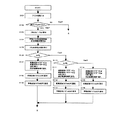
次に、図4及び図1を用いて、本実施例におけるメモリ制御構成を説明する。 Next, a memory control configuration according to the present embodiment will be described with reference to FIGS.
図4に示すように、カートリッジC側には、メモリ30が本体側の読み込み手段36と書き出し手段37と対向して配置されている。また、CPUである制御手段40は、制御部41、演算部42、感光体回転時間検出部43及び帯電バイアス印加時間検出部44などを有する。
As shown in FIG. 4, on the cartridge C side, the
なお、読み込み手段36と書き込み手段37を別々に設ける構成で説明したが、読み込み及び書き込みを行う機能を持つ読み込み/書き込み手段を1つ設ける構成にしても良い。
Although the configuration in which the
制御手段40には、帯電直流バイアス電源50、現像直流バイアス電源60、感光体回転駆動手段70、紙サイズ検知手段80が接続されている。
The
帯電バイアス電源50は、直流制御部51と高圧印加部52とから構成され、現像バイアス電源60は、直流制御部61と高圧印加部62とから構成されている。それぞれ、制御手段からの制御信号に応じて、直流制御部を制御することによって、帯電ローラ2、現像ローラ4に出力するバイアスを制御する。
The charging
また、感光体駆動手段70は、速度制御部71と駆動部72とから構成されており、駆動部72は例えばモータ(不図示)であり、速度制御部71は例えばモータ駆動回路(不図示)である。感光体駆動手段70は、プロセス速度などの動作条件を変更するために、制御手段40からの制御信号を受けて、感光体の駆動速度を変更制御する。
The
紙サイズ検知手段80は、例えば、画像形成装置に用いられる紙サイズを検知するセンサ(不図示)であり、給紙される紙のサイズを検知して検知信号を制御手段に伝達する。制御手段40は、紙サイズ検知手段80からのサイズ検知信号に応じて画像形成動作を制御している。
The paper
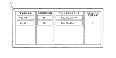
図1にメモリ30内の情報を示す。メモリ30内には様々な情報が格納されているが、本実施例では少なくとも、感光体ドラム使用量情報:A、ドラム使用量を算出するための演算係数情報:ka、kb(感光体回転時間に対する重み付け)、φa、φb(各プロセススピード対する重み付け)、使用量の閾値情報:Bj、Bk、帯電直流バイアスの設定値を特定するデータ:Cai、Caj、Cak(プロセススピードVa)、Cbi、Cbj、Cb(プロセススピードVb)、現像直流バイアスの設定値を特定するデータ: Dai、Daj、Dak(プロセススピードVa)、Dbi、Dbj、Dbk(プロセススピードVb)をメモリ内に記憶する。また、記憶情報の中で演算係数、使用量の閾値情報、プロセス条件を特定するデータ(帯電直流バイアス、現像直流バイアス)は、カートリッジの特性に応じた値であり、かつ、プロセス速度毎に異なる値であり、カートリッジ製造時に書き込まれる。
FIG. 1 shows information in the
本実施例の使用量の閾値情報とプロセス条件を特定するデータを表1に示す。 Table 1 shows the threshold information of the usage amount and the data for specifying the process conditions according to the present embodiment.

さらに、これらメモリ情報は本体制御手段40内の演算部42と常に送受信可能な状態になっており、これら情報を元に演算され、制御部41によってデータの照合が行われている。 Further, the memory information is always in a state where it can be transmitted and received to and from the arithmetic section 42 in the main body control means 40, and is calculated based on the information, and the control section 41 performs data collation.
また、帯電交流バイアス印加時間データと感光体回転時間データとはプリント中に装置本体が計測し、ドラム使用量データの演算は感光体ドラム1の駆動が停止した際に行われて、メモリに更新される。
The charging AC bias application time data and the photoreceptor rotation time data are measured by the apparatus main body during printing, and the calculation of the drum usage data is performed when the driving of the
さらに、本実施例では感光体ドラム使用量Aは下記の式であらわされる。
感光体ドラム使用量A=φa×(ta1+ka×ta2)+φb×(tb1+kb×tb2)
ここで、プロセススピードVaにおける、帯電交流バイアス印加時間をta1、感光体回転時間をta2とし、プロセススピードVbにおける帯電交流バイアス印加時間をtb1、感光体回転時間をtb2とする。
Further, in this embodiment, the photoconductor drum usage amount A is represented by the following equation.
Photoconductor drum usage amount A = φa × (ta1 + ka × ta2) + φb × (tb1 + kb × tb2)
Here, the charging AC bias application time at the process speed Va is ta1, the photoconductor rotation time is ta2, the charging AC bias application time at the process speed Vb is tb1, and the photoconductor rotation time is tb2.
ここで、ka、kb、φa、φbに関しては表2の値を用いたが、以下にその理由を説明する。 Here, the values shown in Table 2 were used for ka, kb, φa, and φb, and the reason will be described below.
本発明者がシーケンス中の本実施例の画像形成装置における感光ドラムの使用量、特に感光ドラムの削れ量について、駆動時間と電圧印加時間の寄与を検討した結果、プロセススピードVaにおいては、感光体ドラムの回転時間に対する削れ量を1としたとき、帯電交流バイアス印加されている場合は2〜3倍程度であることが分かった。 As a result of studying the contribution of the driving time and the voltage application time to the amount of use of the photosensitive drum in the image forming apparatus of the present embodiment during the sequence, particularly the amount of scraping of the photosensitive drum, the process speed Va shows that Assuming that the scraping amount with respect to the rotation time of the drum is 1, when the charging AC bias is applied, it is found that it is about 2 to 3 times.
帯電の交流電圧が印加されている場合は、印加電圧として正負の電圧を交互にし、放電・逆放電を繰り返すために、感光体の表面の劣化が大きく、劣化した感光体表面がクリーニングブレードなどの当接部材との摩擦により削りとられてしまう。 When an alternating voltage for charging is applied, positive and negative voltages are alternately applied as applied voltage, and discharge and reverse discharge are repeated. It is scraped off by friction with the contact member.
また、プロセススピードをVbにした場合、感光体ドラムの回転時間に対する削れ量を1としたとき、帯電交流バイアス印加されている場合は、4.0〜6.0倍程度であることが分かった。また、プロセススピードをVb(Vaの半分の速度)にした場合は、時間当たりの感光体表面の移動距離が半分になるので、クリーニングブレードなどに摺擦する回数が少なくなり、各削れ量はほぼ半分になる。 When the process speed was set to Vb, the amount of scraping with respect to the rotation time of the photosensitive drum was set to 1, and when the charging AC bias was applied, it was found to be about 4.0 to 6.0 times. . Further, when the process speed is set to Vb (half the speed of Va), the moving distance of the photosensitive member surface per time is reduced to half, so that the number of times of rubbing with the cleaning blade or the like is reduced, and each shaving amount is substantially reduced. Halve.
尚、この結果は、感光体としてアリレートとポリカーボネイドを混合した樹脂をメインバインダーとした表層を持つOPC感光体を用い、感光体クリーニングとしてブレードクリーニングを用いた系にて検討することにより得た。 The results were obtained by using an OPC photoreceptor having a surface layer whose main binder was a resin in which arylate and polycarbonate were mixed as the photoreceptor, and examining the system using blade cleaning as the photoreceptor cleaning.
図5に、コントラスト電位とライン幅の関係を示す。ここで、コントラスト電位とは現像バイアス直流成分の電位とドラムVL電位との電位差の絶対値を表す。 FIG. 5 shows the relationship between the contrast potential and the line width. Here, the contrast potential represents the absolute value of the potential difference between the potential of the developing bias DC component and the potential of the drum VL.
図5から分かるように両者はよい相関性を示しており、現像直流バイアス10V当たりのライン幅変化量は、2〜5(μm/10V)である。従って、カートリッジCの使用状態で変動するライン幅を補正するためにはコントラスト電位を制御すればよいことが分かる。本実施例ではコントラスト電位を変更する手段として、現像直流バイアス及び帯電直流バイアスを変更する方法を選んだ。 As can be seen from FIG. 5, the two have a good correlation, and the amount of change in the line width per 10 V of the developing DC bias is 2 to 5 (μm / 10 V). Accordingly, it can be seen that the contrast potential can be controlled in order to correct the line width that fluctuates in the usage state of the cartridge C. In this embodiment, as a means for changing the contrast potential, a method for changing the developing DC bias and the charging DC bias was selected.
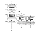
さらに、図6−1、図6−2、図6−3のフローチャートを用いて本実施例の画像形成装置の動作を説明する。本実施例は、記録紙のサイズに応じて画像形成装置のプロセス速度を切り換える機能を有している。例えば、サイズの小さい紙が定着器装置を通過するときに、定着ニップの非通紙領域が過度に昇温することを防止するために、サイズの小さい紙の場合はプロセススピードがVb(Vaの半分の速度)になるような画像形成装置である。 Further, the operation of the image forming apparatus of this embodiment will be described with reference to the flowcharts of FIGS. 6A, 6B, and 6C. The present embodiment has a function of switching the process speed of the image forming apparatus according to the size of the recording paper. For example, in order to prevent the non-sheet passing area of the fixing nip from excessively rising when a small size paper passes through the fixing device, the process speed of the small size paper is Vb (Va (Va)). (Half speed).
また、上記フローチャートに示されるプロセス条件を特定するデータと設定されるプロセス条件を表3に示す。 Table 3 shows data for specifying the process conditions shown in the flowchart and the process conditions to be set.
プリント信号が入力されてから1枚プリントアウトするまでの動作を説明する。 The operation from the input of the print signal to the printing of one sheet will be described.
S101:プリント信号が入力される。 S101: A print signal is input.
S102:制御部40が、給紙カセットの転写材20の幅(定着ローラ長手方向の長さ)が“A4サイズ以上”かどうか確認する。
S102: The
(1−1)Case 1:S102で“A4サイズ以上”=“YES”の場合
S103:制御部40は、プロセススピードを“Va”に設定する。
(1-1) Case 1: If “A4 size or more” = “YES” in S102 S103: The
S104:帯電バイアス印加時間検出部43及び感光体回転時間検出部44がそれぞれ、帯電交流バイアス印加時間及び感光体回転時間のカウントを開始する。 S104: The charging bias application time detection unit 43 and the photoconductor rotation time detection unit 44 start counting the charging AC bias application time and the photoconductor rotation time, respectively.
S105:制御部40が、メモリ内のドラム使用量A情報を受け取る。
S105: The
S106:制御部40がA<Bjであるかどうか確認する。“No”と判断されたときは、S110に進む。ここでBjは感光体ドラムの使用量の閾値情報である(図3参照)。
S106: The
S107:制御部40が“帯電直流バイアスデータ Cai”、“現像直流バイアスデータ Dai”を受け取る。変更するための信号を現像バイアス印加電源直流制御部61及び帯電バイアス印加電源直流制御部51に送る。
S107: The
S108:現像直流バイアスを、−513Vに設定する。 S108: The developing DC bias is set to -513V.
S109:帯電直流バイアスを、−683Vに設定する。 S109: The charging DC bias is set to -683V.
(1−2)Case 2:S106で“A<Bj”=“No”の場合。 (1-2) Case 2: “A <Bj” = “No” in S106.
S110:制御部40がA<Bkであるかどうか確認する。“No”と判断されたときは、S114に進む。ここでBkは感光体ドラムの使用量の閾値情報である(図3参照)。
S110: The
S111:制御部40が“帯電直流バイアスデータ Caj”、“現像直流バイアスデータ Daj”を受け取る。変更するための信号を現像バイアス印加電源直流制御部61及び帯電バイアス印加電源直流制御部51に送る。
S111: The
S112:現像直流バイアスを、−495Vに設定する。 S112: The developing DC bias is set to -495V.
S113:帯電直流バイアスを、−665Vに設定する。 S113: The charging DC bias is set to -665V.
(1−3)Case 3:S110で“A<Bk”=“No”の場合、
S114:制御部40が“帯電直流バイアスデータ Cak”、“現像直流バイアスデータ Dak”と判断する。変更するための信号を現像バイアス印加電源直流制御部61及び帯電バイアス印加電源直流制御部51に送る。
(1-3) Case 3: When “A <Bk” = “No” in S110,
S114: The
S115:現像直流バイアスを、−425Vに設定する。 S115: The developing DC bias is set to -425V.
S116:帯電直流バイアスを、−595Vに設定する。 S116: The charging DC bias is set to -595V.
(1−4)Case 4:S102で“A4サイズ以上”=“No”の場合、
S117:制御部40は、プロセススピードを“Vb”に設定する。
(1-4) Case 4: When “A4 size or more” = “No” in S102,
S117: The
S118:プロセススピード感光体回転時間検出部43及び帯電バイアス印加時間検出部44がそれぞれ、感光体回転時間及び帯電交流バイアス印加時間のカウントを開始する。 S118: The process speed photoconductor rotation time detection unit 43 and the charging bias application time detection unit 44 start counting the photoconductor rotation time and the charging AC bias application time, respectively.
S119:制御部40が、メモリ内のドラム使用量Aを受け取る。
S119: The
S120:制御部40がA<Bjであるかどうか確認する。“No”と判断されたときは、S124に進む。ここでBjは感光体ドラムの使用量の閾値情報である(図3参照)。
S120: The
S121:制御部40が“帯電直流バイアスデータ Cbi”、“現像直流バイアスデータ Dbi”を受け取る。変更するための信号を現像バイアス印加電源直流制御部61及び帯電バイアス印加電源直流制御部516に送る。
S121: The
S122:現像直流バイアスを、−453Vに設定する。 S122: The developing DC bias is set to -453V.
S123:帯電直流バイアスを、−623Vに設定する。 S123: The charging DC bias is set to -623V.
(1−5)Case 5:S120で“A<Bj”=“No”の場合、
S124:制御部40がA<Bkであるかどうか確認する。“No”と判断されたときは、S128に進む。ここでBkは感光体ドラムの使用量の閾値情報である(図3参照)。
(1-5) Case 5: If “A <Bj” = “No” in S120,
S124: The
S125:制御部40が“帯電直流バイアスデータCbj”、“現像直流バイアスデータ Dbj”を受け取る。変更するための信号を現像バイアス印加電源直流制御部61及び帯電バイアス印加電源直流制御部51に送る。
S125: The
S126:現像直流バイアスを、−434Vに設定する。 S126: The developing DC bias is set to -434V.
S127:帯電直流バイアスを、−604Vに設定する。 S127: The charging DC bias is set to -604V.
(1−6)Case 6:S124で“A<Bk”=“No”の場合、
S128:制御部40が“帯電直流バイアスデータ Cbk”、“現像直流バイアスデータ Dbk”を受け取る。変更するための信号を現像バイアス印加電源直流制御部61及び帯電バイアス印加電源直流制御部51に送る。
(1-6) Case 6: If “A <Bk” = “No” in S124,
S128: The
S129:現像直流バイアスを、−415Vに設定する。 S129: The developing DC bias is set to -415V.
S130:帯電直流バイアスを、−585Vに設定する。 S130: The charging DC bias is set to -585V.
S131:画像形成動作スタート。 S131: Start image forming operation.
S132:画像形成動作終了。 S132: The image forming operation ends.
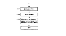
S133:制御部40が、動作した時間内の感光体使用量を求めるために、帯電交流バイアス印加時間に、演算係数(ka、kb)で重み付けした感光体回転時間を加え、プロセススピードの効果を付加するために、各プロセススピード固有の演算係数(φa、φb)によって、重み付けした感光体ドラム使用量ΔAを算出する。書き込み手段がドラムの使用量としてA+ΔAをメモリに書き込む。
これによって、制御動作が終了する(END)。
S133: The
Thereby, the control operation ends (END).
上記のような制御を行った結果により得られたライン幅の推移を図12の一点鎖線として示す。 The transition of the line width obtained as a result of performing the above-described control is shown as a dashed line in FIG.
これより、ライン幅が180〜200μm程度の適正範囲で推移していることが分かり、画像安定性を確保できた。 From this, it was found that the line width was changing in an appropriate range of about 180 to 200 μm, and image stability was secured.
以上説明したように、画像形成前に、ドラム使用量データが所定のドラム使用量の閾値に到達するタイミングで、帯電及び現像直流バイアスを各々のプロセススピードに応じて変更される。その後、特性値の値に応じて使用時に応じた適正バイアスに可変されることにより、安定したライン幅を得ることができる。 As described above, before the image formation, the charging and developing DC biases are changed in accordance with the respective process speeds when the drum usage data reaches the predetermined drum usage threshold. After that, by changing the bias to an appropriate bias according to the characteristic value according to the value of the characteristic value, a stable line width can be obtained.
また、メモリに記憶される感光体ドラムの使用量は、各々のプロセススピード条件ごとの使用量を記憶するのではなく、各プロセススピード条件で重み付けして求めた値を用いているので、メモリ領域の節約になる。 In addition, since the usage amount of the photosensitive drum stored in the memory is not a usage amount for each process speed condition but a value obtained by weighting under each process speed condition, a memory area is used. Savings.
本実施例では、ドラム使用量データの閾値を2つ設けたが、構成の特徴からさらに多数個設けて、それぞれのタイミングでプロセス条件を変更しても良い。 In the present embodiment, two threshold values of the drum usage data are provided, but a larger number may be provided from the characteristics of the configuration, and the process condition may be changed at each timing.
プロセス条件として帯電及び現像電圧を変更したが、場合によっては現像周波数や露光量を変更してもよく、また、使用量データとして、本実施例では演算式の結果を用いたが、印字枚数や感光体回転時間のみの値を使用してもよい。 Although the charging and the developing voltage were changed as the process conditions, the developing frequency and the exposure amount may be changed in some cases.Also, as the use amount data, the result of the arithmetic expression was used in the present embodiment. A value of only the photoconductor rotation time may be used.
実施例2
本実施例では、メモリ内の記憶情報であるプロセススピードごとに領域が確保された、プロセス条件を特定するデータを、帯電直流バイアスと現像直流バイアスで別個に設けるのでなく、組み合わせて1種類のデータとして記憶している。
図7に本実施例のメモリ領域について示す。Eai、Eaj、Eak、Ebi、Ebj、Ebkが組み合わせデータであり、このうち1つのデータを制御手段が受け取ると、制御手段は帯電直流バイアス印加電源制御部と現像直流バイアス印加電源制御部のそれぞれに対して、制御信号を発信する。
Example 2
In this embodiment, data for specifying process conditions, in which an area is secured for each process speed, which is information stored in the memory, is not separately provided by the charging DC bias and the developing DC bias, but is combined with one type of data. It is remembered as.
FIG. 7 shows the memory area of this embodiment. Eai, Eaj, Eak, Ebi, Ebj, and Ebk are combination data. When one of the data is received by the control unit, the control unit sends the data to the charging DC bias application power supply control unit and the developing DC bias application power supply control unit. In response, a control signal is transmitted.
また、帯電直流バイアスと現像直流バイアスの値の組み合わせは、かぶり防止のためにバックコントラストをほぼ一定にしつつ、現像コントラストを変更する必要がある。 In addition, the combination of the charging DC bias and the developing DC bias needs to change the developing contrast while keeping the back contrast substantially constant in order to prevent fogging.
本実施例の組み合わせたデータと、帯電直流バイアス値と現像直流バイアス値のテーブルを表4に示す。 Table 4 shows the combined data of this embodiment and a table of the charging DC bias value and the developing DC bias value.
このようにして、実施例1の効果の他にメモリ内のプロセス条件を特定するデータ1つに対して、複数のプロセスユニットを制御できるので、メモリ領域の節約になる。 In this manner, in addition to the effects of the first embodiment, a plurality of process units can be controlled for one piece of data that specifies a process condition in a memory, so that a memory area can be saved.
また、本実施例のプロセス条件を特定するデータは、ユーザーが濃度調整を行うために装置本体内に備わった濃度調整テーブルを利用しても良く、その場合はメモリに記憶されるのは濃度調整の設定値を特定するデータになる。 Further, the data for specifying the process conditions of the present embodiment may use a density adjustment table provided in the apparatus main body for the user to perform the density adjustment. In this case, the density adjustment table is stored in the memory. Is data that specifies the set value of.
さらに、帯電直流バイアス、現像直流バイアスの組み合わせだけでなく、露光量などを組み合わせたデータでもよい。 Further, not only a combination of the charging DC bias and the developing DC bias, but also data obtained by combining an exposure amount and the like may be used.
以上説明したように、使用量の異なったカートリッジが動作条件の違いによって生じる画像のばらつきを補正でき、安定した画像を提供することができる。 As described above, it is possible to correct a variation in an image caused by a cartridge having a different usage amount due to a difference in an operation condition, and to provide a stable image.
C カートリッジ
L レーザービームプリンタ
1 感光体ドラム
2 接触帯電ローラ
3 レーザユニット
4 現像スリーブ
5 現像ブレード
6 トナー容器
7a、7b 攪拌手段
8 転写ローラ
9 クリーニングブレード
10 廃トナー容器
11 定着ユニット
20 記録媒体
21 給紙ローラ
22 レジローラ
30 メモリ
31 感光体ドラム使用量の記憶領域(第1の記憶領域)
32 閾値の記憶領域(第2の記憶領域)
33a、33b、33b プロセス条件を特定するデータを記憶する領域(複数の記憶領域)
34a、34b、34b 感光体ドラム使用量を算出するための演算係数(複数の記憶領域)
35 伝達手段
36 読み込み手段
37 書き出し手段
38 制御伝達部
40 制御手段
41 制御部
42 演算部
43 感光体回転駆動時間検出部
44 帯電交流バイアス印加時間検出部
45 現像バイアス印加電源直流制御部
46 帯電バイアス印加電源直流制御部
C Cartridge L
32 Threshold storage area (second storage area)
33a, 33b, 33b Areas for storing data specifying process conditions (a plurality of storage areas)
34a, 34b, 34b Operation coefficients (a plurality of storage areas) for calculating the photosensitive drum usage amount
35 transmission means 36 reading means 37 writing means 38
Claims (24)
画像形成装置本体は、前記画像形成条件を設定する制御ユニットを有し、
前記制御ユニットは、前記画像形成速度に対応した前記プロセス要素の画像形成条件に係わる情報に基づいて、前記画像形成速度に応じた画像形成条件を設定することを特徴とする画像形成装置。 An image forming apparatus in which a cartridge is mountable and capable of forming an image at a plurality of image forming speeds, wherein the cartridge stores information relating to image forming conditions of a process element corresponding to the image forming speed. A memory medium having one storage area,
The image forming apparatus main body has a control unit for setting the image forming conditions,
The image forming apparatus, wherein the control unit sets an image forming condition corresponding to the image forming speed based on information about an image forming condition of the process element corresponding to the image forming speed.
前記画像形成速度は前記像担持体の回転速度を含み、
前記制御装置は、前記像担持体の回転速度に対応した画像形成条件を設定することを特徴とする請求項1に記載の画像形成装置。 The process element includes at least an image carrier,
The image forming speed includes a rotation speed of the image carrier,
The image forming apparatus according to claim 1, wherein the control device sets an image forming condition corresponding to a rotation speed of the image carrier.
前記画像形成条件は、前記帯電部材または前記現像部材に印加するバイアスを含むことを特徴とする請求項1ないし5のいずれかに記載の画像形成装置。 The process element includes an image carrier, a charging member for charging the image carrier, a developing member for developing a latent image on the image carrier,
The image forming apparatus according to claim 1, wherein the image forming condition includes a bias applied to the charging member or the developing member.
前記メモリ媒体は、前記画像形成速度に対応した前記プロセス要素の画像形成条件に係わる情報を記憶するための第1の記憶領域を有することを特徴とするカートリッジ。 In a cartridge which is detachable from an image forming apparatus main body capable of forming an image under a plurality of image forming conditions and is provided with a part of a process element for forming an image and a memory medium,
The cartridge according to claim 1, wherein the memory medium has a first storage area for storing information related to an image forming condition of the process element corresponding to the image forming speed.
前記画像形成条件は前記像担持体の回転速度を含むことを特徴とする請求項7ないし9のいずれかに記載のカートリッジ。 The process element includes at least an image carrier,
10. The cartridge according to claim 7, wherein the image forming condition includes a rotation speed of the image carrier.
前記画像形成条件は、前記帯電部材または前記現像部材に印加するバイアスを含むことを特徴とする請求項7ないし9のいずれかに記載のカートリッジ。 The process element includes an image carrier, a charging member for charging the image carrier, a developing member for developing a latent image on the image carrier,
10. The cartridge according to claim 7, wherein the image forming condition includes a bias applied to the charging member or the developing member.
前記画像形成速度に対応した前記プロセス要素の画像形成条件に係わる情報を記憶するための第1の記憶領域を有することを特徴とするメモリ媒体。 In a memory medium which is detachable from an image forming apparatus main body capable of forming an image under a plurality of image forming conditions and is mounted on a cartridge having a part of a process element for performing image formation,
A memory medium having a first storage area for storing information relating to image forming conditions of the process element corresponding to the image forming speed.
前記画像形成速度は前記像担持体の回転速度を含むことを特徴とする請求項13ないし15のいずれかに記載のメモリ媒体。 The process element includes at least an image carrier,
16. The memory medium according to claim 13, wherein the image forming speed includes a rotation speed of the image carrier.
前記画像形成条件は、前記帯電部材または前記現像部材に印加するバイアスを含むことを特徴とする請求項13ないし16のいずれかに記載のメモリ媒体。 The process element includes an image carrier, a charging member for charging the image carrier, a developing member for developing a latent image on the image carrier,
17. The memory medium according to claim 13, wherein the image forming condition includes a bias applied to the charging member or the developing member.
前記画像形成装置は、画像形成を行うためのプロセス要素の一部を有し、
前記システムは、前記カートリッジに搭載されるメモリ媒体を有し、
前記メモリ媒体は、前記画像形成速度に対応した前記プロセス要素の画像形成条件に係わる情報を記憶するための第1の記憶領域を有し、
更に、前記画像形成条件を設定する制御ユニットを有し、
前記制御ユニットは、前記画像形成速度に対応した前記プロセス要素の画像形成条件に係わる情報に基づいて、前記画像形成速度に応じた画像形成条件を設定することを特徴とする画像形成システム。 In an image forming system of an image forming apparatus having an apparatus main body and a cartridge and capable of forming an image under a plurality of image forming conditions,
The image forming apparatus has a part of a process element for performing image formation,
The system includes a memory medium mounted on the cartridge,
The memory medium has a first storage area for storing information related to an image forming condition of the process element corresponding to the image forming speed,
A control unit for setting the image forming conditions;
The image forming system according to claim 1, wherein the control unit sets an image forming condition corresponding to the image forming speed based on information about an image forming condition of the process element corresponding to the image forming speed.
前記画像形成速度は前記像担持体の速度を含み、
前記制御装置は、前記像担持体の速度に対応した画像形成条件を設定することを特徴とする請求項19に記載の画像形成装置システム。 The process element includes at least an image carrier,
The image forming speed includes the speed of the image carrier,
20. The image forming apparatus system according to claim 19, wherein the control device sets an image forming condition corresponding to a speed of the image carrier.
前記画像形成条件は、前記帯電部材または前記現像部材に印加するバイアスを含むことを特徴とする請求項19ないし22のいずれかに記載の画像形成システム。 The process element includes an image carrier, a charging member for charging the image carrier, a developing member for developing a latent image on the image carrier,
23. The image forming system according to claim 19, wherein the image forming condition includes a bias applied to the charging member or the developing member.
Priority Applications (6)
| Application Number | Priority Date | Filing Date | Title |
|---|---|---|---|
| JP2003370552A JP2004170955A (en) | 2002-11-08 | 2003-10-30 | Image forming apparatus, cartridge, image forming system and memory medium for cartridge |
| RU2003132651/28A RU2266553C2 (en) | 2002-11-08 | 2003-11-06 | Image forming device, cartridge, image forming system and memorizing medium for cartridge |
| EP03025712.5A EP1434106B1 (en) | 2002-11-08 | 2003-11-07 | Image forming apparatus, process cartridge, image formation system, and storage medium for cartridge |
| US10/702,658 US7274884B2 (en) | 2002-11-08 | 2003-11-07 | Image forming apparatus to which a cartridge having a memory medium configured to store information-forming-condition information is attachable, such a cartridge, such a memory medium, and an image forming system comprising such a memory medium |
| KR10-2003-0078836A KR100532181B1 (en) | 2002-11-08 | 2003-11-08 | Image Forming Apparatus, Cartridge, Image Formation System, and Storage Medium for Cartridge |
| CNB2003101132777A CN100367131C (en) | 2002-11-08 | 2003-11-10 | Imaging appts. cartridge parts, imaging system and storage medium for cartridge |
Applications Claiming Priority (2)
| Application Number | Priority Date | Filing Date | Title |
|---|---|---|---|
| JP2002325797 | 2002-11-08 | ||
| JP2003370552A JP2004170955A (en) | 2002-11-08 | 2003-10-30 | Image forming apparatus, cartridge, image forming system and memory medium for cartridge |
Publications (2)
| Publication Number | Publication Date |
|---|---|
| JP2004170955A true JP2004170955A (en) | 2004-06-17 |
| JP2004170955A5 JP2004170955A5 (en) | 2006-12-14 |
Family
ID=32473636
Family Applications (1)
| Application Number | Title | Priority Date | Filing Date |
|---|---|---|---|
| JP2003370552A Pending JP2004170955A (en) | 2002-11-08 | 2003-10-30 | Image forming apparatus, cartridge, image forming system and memory medium for cartridge |
Country Status (6)
| Country | Link |
|---|---|
| US (1) | US7274884B2 (en) |
| EP (1) | EP1434106B1 (en) |
| JP (1) | JP2004170955A (en) |
| KR (1) | KR100532181B1 (en) |
| CN (1) | CN100367131C (en) |
| RU (1) | RU2266553C2 (en) |
Cited By (5)
| Publication number | Priority date | Publication date | Assignee | Title |
|---|---|---|---|---|
| WO2006025361A1 (en) * | 2004-09-01 | 2006-03-09 | Seiko Epson Corporation | Image formation device and image formation method |
| JP2006163236A (en) * | 2004-12-10 | 2006-06-22 | Fuji Xerox Co Ltd | Image forming apparatus |
| JP2010181841A (en) * | 2009-02-09 | 2010-08-19 | Canon Inc | Image forming apparatus and method for controlling the same |
| JP2017044930A (en) * | 2015-08-28 | 2017-03-02 | キヤノン株式会社 | Image forming apparatus |
| JP2018004821A (en) * | 2016-06-29 | 2018-01-11 | コニカミノルタ株式会社 | Image formation apparatus |
Families Citing this family (28)
| Publication number | Priority date | Publication date | Assignee | Title |
|---|---|---|---|---|
| JP4439994B2 (en) * | 2003-05-14 | 2010-03-24 | キヤノン株式会社 | Image forming apparatus, cartridge, and storage device mounted on cartridge |
| CN100407067C (en) * | 2003-05-14 | 2008-07-30 | 佳能株式会社 | Image forming apparatus, cartridge, and storing device mounted to the cartridge |
| JP2006003464A (en) * | 2004-06-15 | 2006-01-05 | Canon Inc | Development device, image forming apparatus and cartridge |
| CN1746783B (en) * | 2004-09-10 | 2012-03-28 | 佳能株式会社 | Image forming apparatus and cartridge |
| KR100577715B1 (en) | 2004-12-01 | 2006-05-10 | 삼성전자주식회사 | Image forming device and controlling method thereof |
| JP4280770B2 (en) | 2006-01-11 | 2009-06-17 | キヤノン株式会社 | Process cartridge and electrophotographic image forming apparatus |
| US7991311B2 (en) * | 2006-10-26 | 2011-08-02 | Aetas Technology Incorporated | Image forming apparatus and method for controlling developing bias voltage |
| JP4498407B2 (en) | 2006-12-22 | 2010-07-07 | キヤノン株式会社 | Process cartridge, electrophotographic image forming apparatus, and electrophotographic photosensitive drum unit |
| KR100892110B1 (en) | 2008-02-22 | 2009-04-08 | 삼성전자주식회사 | Developing cartridge, image forming apparatus having the same, and printing method for an image forming apparatus |
| KR100915397B1 (en) | 2008-02-22 | 2009-09-03 | 삼성전자주식회사 | Cover member, developing cartridge and developing unit for image forming apparatus |
| KR100915396B1 (en) | 2008-02-22 | 2009-09-03 | 삼성전자주식회사 | Toner cartridge, a devloping unit and image forming apparatus having the same |
| KR100912900B1 (en) | 2008-02-22 | 2009-08-20 | 삼성전자주식회사 | Developer cartrage, developing device and image forming apparatus having the same |
| KR100933290B1 (en) | 2008-02-22 | 2009-12-22 | 삼성전자주식회사 | A memory unit, a developer cartridge, a developing apparatus and an image forming apparatus including the same |
| KR100899350B1 (en) | 2008-02-22 | 2009-05-27 | 삼성전자주식회사 | Developing apparatus, image forming apparatus having the same, and toner suppling method for a developing apparatus |
| JP4968957B2 (en) * | 2008-03-31 | 2012-07-04 | キヤノン株式会社 | Frame body unit, developing device and process cartridge, and frame body unit, developing device and process cartridge manufacturing method |
| KR101314933B1 (en) * | 2008-08-04 | 2013-10-04 | 캐논 가부시끼가이샤 | Magnetic carrier and two-component developer |
| US8064808B2 (en) * | 2008-08-25 | 2011-11-22 | Canon Kabushiki Kaisha | Developing roller, and electrophotographic process cartridge and electrophotographic image forming apparatus comprising the developing roller |
| US8275262B2 (en) * | 2008-11-10 | 2012-09-25 | At&T Intellectual Property I, L.P. | Methods and apparatus to deploy fiber optic based access networks |
| US20100164979A1 (en) * | 2008-12-26 | 2010-07-01 | Kyocera Mita Corporation | Image forming apparatus and image forming method |
| JP5297917B2 (en) * | 2009-06-30 | 2013-09-25 | 京セラドキュメントソリューションズ株式会社 | Cleaning device, image forming device |
| JP2014178636A (en) * | 2013-03-15 | 2014-09-25 | Ricoh Co Ltd | Fixing device, and image forming apparatus |
| EP2977820B1 (en) | 2014-07-25 | 2021-02-17 | Canon Kabushiki Kaisha | Cartridge and image forming apparatus |
| EP3051360B1 (en) | 2015-01-30 | 2022-05-25 | Canon Kabushiki Kaisha | Developing apparatus, process cartridge and image forming apparatus |
| MX359573B (en) * | 2015-05-15 | 2018-09-24 | Hewlett Packard Development Co | Printer cartridges and memory devices containing compressed multi-dimensional color tables. |
| US9910395B2 (en) * | 2016-07-19 | 2018-03-06 | Lexmark International, Inc. | Systems and methods for controlling toner development in an image forming device |
| JP7211089B2 (en) * | 2019-01-15 | 2023-01-24 | ブラザー工業株式会社 | Image forming apparatus, image forming program, and image forming method |
| US11036161B2 (en) | 2019-04-18 | 2021-06-15 | Canon Kabushiki Kaisha | Developer bearing member, developing apparatus, process cartridge, and image forming apparatus |
| JP2020177229A (en) * | 2019-04-18 | 2020-10-29 | キヤノン株式会社 | Developer carrier, developing device, process cartridge, and image forming apparatus |
Family Cites Families (13)
| Publication number | Priority date | Publication date | Assignee | Title |
|---|---|---|---|---|
| US5276461A (en) * | 1989-04-18 | 1994-01-04 | Tokyo Electric Co., Ltd. | Electrophotographic printing device |
| US5272503A (en) | 1992-09-02 | 1993-12-21 | Xerox Corporation | Replaceable sub-assemblies for electrostatographic reproducing machines |
| JPH07244419A (en) | 1994-03-04 | 1995-09-19 | Fuji Xerox Co Ltd | Electrophotographic method |
| US6597876B1 (en) * | 1999-10-15 | 2003-07-22 | Canon Kabushiki Kaisha | Image forming apparatus and cartridge detachably mountable thereto |
| JP2001117468A (en) | 1999-10-15 | 2001-04-27 | Canon Inc | Memory medium for process cartridge, process cartridge, device and system for forming electrophotographic image |
| JP2001117425A (en) | 1999-10-15 | 2001-04-27 | Canon Inc | Memory medium for process cartridge, process cartridge, device and system for forming electrophotographic image |
| JP2002062780A (en) * | 2000-08-16 | 2002-02-28 | Canon Inc | Apparatus and method for forming image |
| JP2002072573A (en) * | 2000-08-23 | 2002-03-12 | Canon Inc | Image-forming device, cartridge image-forming system and storage medium |
| JP2002091098A (en) | 2000-09-18 | 2002-03-27 | Canon Inc | Electrophotographic image forming device and process cartridge |
| US6549223B2 (en) * | 2000-12-12 | 2003-04-15 | Canon Kabushiki Kaisha | Electrophotographic apparatus, process cartridge, and electrophotographic photosensitive member |
| JP2002214983A (en) * | 2001-01-15 | 2002-07-31 | Canon Inc | Image forming device and life detecting method for its image carrier, and cartridge attachable to and detachable from the device |
| US6714746B2 (en) | 2001-01-23 | 2004-03-30 | Canon Kabushiki Kaisha | Image forming apparatus rotationally driving image bearing member and contact electrifying member of process cartridge and process cartridge comprising image bearing member and contact electrifying member |
| JP2002351287A (en) | 2001-03-23 | 2002-12-06 | Ricoh Co Ltd | Imaging unit and image forming device |
-
2003
- 2003-10-30 JP JP2003370552A patent/JP2004170955A/en active Pending
- 2003-11-06 RU RU2003132651/28A patent/RU2266553C2/en not_active IP Right Cessation
- 2003-11-07 US US10/702,658 patent/US7274884B2/en active Active
- 2003-11-07 EP EP03025712.5A patent/EP1434106B1/en not_active Expired - Lifetime
- 2003-11-08 KR KR10-2003-0078836A patent/KR100532181B1/en not_active IP Right Cessation
- 2003-11-10 CN CNB2003101132777A patent/CN100367131C/en not_active Expired - Fee Related
Cited By (7)
| Publication number | Priority date | Publication date | Assignee | Title |
|---|---|---|---|---|
| WO2006025361A1 (en) * | 2004-09-01 | 2006-03-09 | Seiko Epson Corporation | Image formation device and image formation method |
| US7664412B2 (en) | 2004-09-01 | 2010-02-16 | Seiko Epson Corporation | Image forming apparatus that adjusts operating conditions based on a density detection result of a patch image |
| JP2006163236A (en) * | 2004-12-10 | 2006-06-22 | Fuji Xerox Co Ltd | Image forming apparatus |
| JP4736412B2 (en) * | 2004-12-10 | 2011-07-27 | 富士ゼロックス株式会社 | Image forming apparatus |
| JP2010181841A (en) * | 2009-02-09 | 2010-08-19 | Canon Inc | Image forming apparatus and method for controlling the same |
| JP2017044930A (en) * | 2015-08-28 | 2017-03-02 | キヤノン株式会社 | Image forming apparatus |
| JP2018004821A (en) * | 2016-06-29 | 2018-01-11 | コニカミノルタ株式会社 | Image formation apparatus |
Also Published As
| Publication number | Publication date |
|---|---|
| RU2003132651A (en) | 2005-04-20 |
| EP1434106A2 (en) | 2004-06-30 |
| CN100367131C (en) | 2008-02-06 |
| EP1434106B1 (en) | 2015-05-27 |
| KR20040041077A (en) | 2004-05-13 |
| US20040131370A1 (en) | 2004-07-08 |
| EP1434106A3 (en) | 2011-04-20 |
| US7274884B2 (en) | 2007-09-25 |
| CN1499320A (en) | 2004-05-26 |
| RU2266553C2 (en) | 2005-12-20 |
| KR100532181B1 (en) | 2005-11-30 |
Similar Documents
| Publication | Publication Date | Title |
|---|---|---|
| JP2004170955A (en) | Image forming apparatus, cartridge, image forming system and memory medium for cartridge | |
| US7095966B2 (en) | Image forming apparatus and unit, and storage medium mounted in the unit | |
| JP2003330320A (en) | Image forming device | |
| US20080285993A1 (en) | Image forming apparatus | |
| JP4976872B2 (en) | Image forming apparatus | |
| JP5054316B2 (en) | Image forming apparatus | |
| JP2004170956A (en) | Image forming apparatus, cartridge, image forming system and memory medium for cartridge | |
| JP2002072573A (en) | Image-forming device, cartridge image-forming system and storage medium | |
| US8488985B2 (en) | Image forming apparatus and method for applying transfer voltage in the image forming apparatus | |
| JP2006227325A (en) | Image forming apparatus | |
| JP2001117425A (en) | Memory medium for process cartridge, process cartridge, device and system for forming electrophotographic image | |
| JP2010210799A (en) | Lubricant application mechanism, process cartridge and image forming apparatus | |
| JP5103843B2 (en) | Image forming apparatus | |
| US6546214B2 (en) | Image forming apparatus comprising storing means for storing a parameter regarding an accumulation operation amount of the apparatus or of a cartridge detachably mountable to the apparatus | |
| JP6708425B2 (en) | Image forming device | |
| JP2022080957A (en) | Image formation apparatus | |
| JP2003307994A (en) | Image forming apparatus, cartridge, process control system and storage medium | |
| US9846400B2 (en) | Image forming apparatus that executes light emission based on discharge dot count value | |
| JP2006337704A (en) | Storing medium, cartridge, and image forming apparatus | |
| JP2004085812A (en) | Toner cartridge | |
| JP7424032B2 (en) | image forming device | |
| JP2005338636A (en) | Cleaner-less type image forming apparatus | |
| JP6314852B2 (en) | Developing device and image forming apparatus having the same | |
| JP2007065486A (en) | Developing apparatus, image forming mechanism, image forming apparatus and control method of developing apparatus | |
| JP6738530B2 (en) | Image forming device |
Legal Events
| Date | Code | Title | Description |
|---|---|---|---|
| A521 | Request for written amendment filed |
Free format text: JAPANESE INTERMEDIATE CODE: A523 Effective date: 20061027 |
|
| A621 | Written request for application examination |
Free format text: JAPANESE INTERMEDIATE CODE: A621 Effective date: 20061027 |
|
| A977 | Report on retrieval |
Free format text: JAPANESE INTERMEDIATE CODE: A971007 Effective date: 20080916 |
|
| A131 | Notification of reasons for refusal |
Free format text: JAPANESE INTERMEDIATE CODE: A131 Effective date: 20081118 |
|
| A521 | Request for written amendment filed |
Free format text: JAPANESE INTERMEDIATE CODE: A523 Effective date: 20090119 |
|
| A131 | Notification of reasons for refusal |
Free format text: JAPANESE INTERMEDIATE CODE: A131 Effective date: 20090414 |
|
| A521 | Request for written amendment filed |
Free format text: JAPANESE INTERMEDIATE CODE: A523 Effective date: 20090615 |
|
| A02 | Decision of refusal |
Free format text: JAPANESE INTERMEDIATE CODE: A02 Effective date: 20090728 |