JP2004158686A - Solid-state image sensing device - Google Patents
Solid-state image sensing device Download PDFInfo
- Publication number
- JP2004158686A JP2004158686A JP2002323859A JP2002323859A JP2004158686A JP 2004158686 A JP2004158686 A JP 2004158686A JP 2002323859 A JP2002323859 A JP 2002323859A JP 2002323859 A JP2002323859 A JP 2002323859A JP 2004158686 A JP2004158686 A JP 2004158686A
- Authority
- JP
- Japan
- Prior art keywords
- light
- light receiving
- solid
- imaging surface
- photosensitive
- Prior art date
- Legal status (The legal status is an assumption and is not a legal conclusion. Google has not performed a legal analysis and makes no representation as to the accuracy of the status listed.)
- Granted
Links
- 230000035945 sensitivity Effects 0.000 claims abstract description 28
- 230000003287 optical effect Effects 0.000 claims abstract description 19
- 230000002093 peripheral effect Effects 0.000 claims abstract description 19
- 238000003384 imaging method Methods 0.000 claims description 140
- 239000011159 matrix material Substances 0.000 claims description 2
- 230000007423 decrease Effects 0.000 abstract description 10
- 230000004907 flux Effects 0.000 abstract description 5
- 229910021420 polycrystalline silicon Inorganic materials 0.000 description 5
- 229920005591 polysilicon Polymers 0.000 description 5
- 238000006243 chemical reaction Methods 0.000 description 4
- 238000013459 approach Methods 0.000 description 3
- 238000003705 background correction Methods 0.000 description 2
- 230000001154 acute effect Effects 0.000 description 1
- 230000015556 catabolic process Effects 0.000 description 1
- 238000006731 degradation reaction Methods 0.000 description 1
- 230000006866 deterioration Effects 0.000 description 1
- 230000000694 effects Effects 0.000 description 1
- 230000001678 irradiating effect Effects 0.000 description 1
- 229910044991 metal oxide Inorganic materials 0.000 description 1
- 150000004706 metal oxides Chemical class 0.000 description 1
- 210000001747 pupil Anatomy 0.000 description 1
- 239000004065 semiconductor Substances 0.000 description 1
Images


Classifications
-
- H—ELECTRICITY
- H01—ELECTRIC ELEMENTS
- H01L—SEMICONDUCTOR DEVICES NOT COVERED BY CLASS H10
- H01L27/00—Devices consisting of a plurality of semiconductor or other solid-state components formed in or on a common substrate
- H01L27/14—Devices consisting of a plurality of semiconductor or other solid-state components formed in or on a common substrate including semiconductor components sensitive to infrared radiation, light, electromagnetic radiation of shorter wavelength or corpuscular radiation and specially adapted either for the conversion of the energy of such radiation into electrical energy or for the control of electrical energy by such radiation
- H01L27/144—Devices controlled by radiation
- H01L27/146—Imager structures
- H01L27/14643—Photodiode arrays; MOS imagers
-
- H—ELECTRICITY
- H01—ELECTRIC ELEMENTS
- H01L—SEMICONDUCTOR DEVICES NOT COVERED BY CLASS H10
- H01L27/00—Devices consisting of a plurality of semiconductor or other solid-state components formed in or on a common substrate
- H01L27/14—Devices consisting of a plurality of semiconductor or other solid-state components formed in or on a common substrate including semiconductor components sensitive to infrared radiation, light, electromagnetic radiation of shorter wavelength or corpuscular radiation and specially adapted either for the conversion of the energy of such radiation into electrical energy or for the control of electrical energy by such radiation
- H01L27/144—Devices controlled by radiation
- H01L27/146—Imager structures
- H01L27/14601—Structural or functional details thereof
- H01L27/14603—Special geometry or disposition of pixel-elements, address-lines or gate-electrodes
-
- H—ELECTRICITY
- H01—ELECTRIC ELEMENTS
- H01L—SEMICONDUCTOR DEVICES NOT COVERED BY CLASS H10
- H01L27/00—Devices consisting of a plurality of semiconductor or other solid-state components formed in or on a common substrate
- H01L27/14—Devices consisting of a plurality of semiconductor or other solid-state components formed in or on a common substrate including semiconductor components sensitive to infrared radiation, light, electromagnetic radiation of shorter wavelength or corpuscular radiation and specially adapted either for the conversion of the energy of such radiation into electrical energy or for the control of electrical energy by such radiation
- H01L27/144—Devices controlled by radiation
- H01L27/146—Imager structures
- H01L27/14601—Structural or functional details thereof
- H01L27/14625—Optical elements or arrangements associated with the device
- H01L27/14627—Microlenses
Abstract
Description
【0001】
【発明の属する技術分野】
本発明は、被写界からの入射光が入射される撮像面の各画素において、感度の異なる複数の感光部が配置された受光部、およびこの受光部に入射光を集光するマイクロレンズを備えた固体撮像素子に関するものである。
【0002】
【従来の技術】
従来から、固体撮像素子は、各画素に対応する受光部において、開口部の大きさが異なる主感光部と従感光部とを形成することによって感度差をもたせ、広ダイナミックレンジ化を実現している。このとき、主感光部は、開口部が大きく、感度が高い感光部であり、一定以上の入射光量が特定できなくなるものであるが、従感光部は、開口部が小さく、感度の低い感光部であり、主感光部に比べて飽和しにくいため適切な入射光量を求めることができる。したがって、これらの感光部の信号出力を各画素ごとに混合することによって画像信号を広いダイナミックレンジで得ている。
【0003】
ところで、固体撮像素子が出力する画像信号は、さまざまな原因により各受光部における受光光量が不均一となるシェーディングが発生する。マイクロレンズが形成された固体撮像素子を用いたディジタルカメラの場合、入射光がマイクロレンズによって集光されて受光部に入射するため、実質的に開口率が向上しているが、その入射角度によって各受光部における受光光量は変化する。一般的には、固体撮像素子の周縁部では傾斜して入射する入射光が多く、その傾斜の方向が偏るため、中心部に比べて受光部における受光光量が低下する。このため、撮影した画像の周縁部において輝度が低下するといういわゆるシェーディングが発生する。従来から、シェーディングが生じた画像信号は、ディジタル処理やメモリなどを使用することにより補正され、その補正回路の簡素化が可能になっている。
【0004】
しかし、固体撮像素子では、画素に対応する受光部に感度の異なる複数の感光部を形成してダイナミックレンジの拡大を図ると、感光部ごとに光電変換特性などが異なるため、適切なシェーディング補正ができない。そこで、この適切なシェーディング補正を行なうために、特許文献1では、感度の低い受光素子(すなわち上述の感光部)を、各画素において撮像画面の中心から遠い側に配置し、たとえば、各画素の受光部において感度の高い受光素子に対して左右上下のいずれかの位置に、全体としては画面中心に対して対称に配置する固体撮像素子を備えることによって、シェーディングの偏りを防ぎ、これら感度の異なる受光素子でも共通のシェーディング補正を行う固体撮像装置が知られている。
【0005】
【特許文献1】
特願2002−228562。
【0006】
【発明が解決しようとする課題】
上に記載するような固体撮像素子は、ディジタルスチルカメラなどの固体撮像装置に適用すると、固体撮像素子の撮像面18が図3に示すように設置されて、撮像面18の被写体側に置かれた絞り機構(図示せず)の絞り値が小さい場合、または光学系レンズ34の射出瞳位置と撮像面18との距離が短い場合などでは、撮像面18に対して傾斜して入射する入射光が相対的に増加する。特に撮像面18の周縁部では、周縁方向に向かって傾斜して入射する入射光が多く、より鋭角に入射するものもある。
【0007】
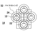
この撮像面18は、図5に示すように、各画素に対応する受光部12を複数個有し、各受光部12は、主感光部22および従感光部24を含み、これらの感光部に光束を集光するマイクロレンズ52を各受光部ごとに備えている。このとき、撮像面18への入射光は、その入射角によってはこのマイクロレンズ52で大きく屈折され、この屈折された光束は、各感光部22および24に入射しにくくなる。
【0008】
たとえば、撮像面18に垂直に入射する入射光602は、図8に示すように、マイクロレンズ52によって都合よく集光され、主感光部の開口部62、および従感光部の開口部64に多くの光束を入射させることができるが、撮像面18に斜めに入射する入射光604は、図9や図10に示すように、マイクロレンズ52によって大きく屈折され、各感光部の開口部62および64に入射する光束が減少し、集光率が低下する。特に、従感光部24は、開口部64が小さいために集光率が低下しやすく、その感度がさらに低下する。
【0009】
このように、固体撮像素子10の撮像面18において、斜めに入射する入射光が多い画素位置では、感度低下が起こりやすく、そのため、撮影した画像にはシェーディングが発生する。また、光束の入射角によって各感光部22および24の集光率が大きく変化するため、シェーディング形状(プロファイル)が変化することもある。
【0010】
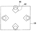
また、入射光は、撮像面18上で結像する際に、光学系レンズ34により集光されて錯乱円(イメージサークル)44を出現させるが、上述のように光束が斜めに入射すると撮像面18の周縁方向にずれて集光されるため、図4に示すように、錯乱円44は、受光部の開口部42から撮像面18の周縁方向にずれた位置に出現する。この錯乱円44は、撮像面18の周縁部に近づくに従って、受光部の開口部42から大きくずれる。この撮像面18の各受光部12において、図5に示すように、従感光部24が主感光部24の上方に備えられている場合、図4に示すような錯乱円44が出現すると、特に、撮像面18の下側の画素位置では、従感光部24における集光率が低下する。
【0011】
この撮像面18の平面における上側の画素位置の受光部12では、図9に示すように、斜めの入射光604が多いとき、各感光部の開口部62および64に入射する光束は減少するが、主感光部の開口部62は、受光可能な領域が大きいため、また従感光部の開口部64は、撮像面18の周縁部に近く、集光される方向に位置するため、光束を集めることは比較的容易である。一方、撮像面18の下側の画素位置では、図10に示すように、マイクロレンズ52で集光された光束は、主感光部の開口部62には入射しやすいが、従感光部の開口部64には入射しにくく、その入射角によっては入射しないことがあり、集光率が低下しやすい。このように、撮像面18の上側と下側とで、従感光部24の受光光量に差が生じるため、撮影した画像の上下で非対称な輝度シェーディングが発生しやすくなる。
【0012】
本発明はこのような従来技術の欠点を解消し、特に低感度の感光部における感度低下を低減させ、さらには撮像面、特にその周縁部に発生するシェーディングを低減させて画像品質の低下を防ぐことができる固体撮像素子を提供することを目的とする。
【0013】
【課題を解決するための手段】
本発明によれば、被写界からの入射光を結像する撮像面を含み、この撮像面は、行および列方向に配列されこの撮像面を形成する各画素に対応する複数の受光部、およびこの複数の受光部のそれぞれに備えられて入射光を集光するマイクロレンズを含み、この複数の受光部のそれぞれは、第1の感度を有し、この入射光を光電変換する第1の感光部と、第1の感度より低い第2の感度を有し、この入射光を光電変換する第2の感光部とを含む固体撮像素子は、このマイクロレンズは、その光学中心をこの受光部の中心からこの撮像面の中心寄りにずらして設置されていることを特徴とする。
【0014】
【発明の実施の形態】
次に添付図面を参照して本発明による固体撮像素子の実施例を詳細に説明する。
【0015】
実施例の固体撮像素子では、画素に対応する受光部は、複数の感光部を用いて、各感光部の開口部の大きさに差をもたらすことにより、感度、すなわち光電変換効率を変え、ダイナミックレンジの拡大を図っている。これらの感光部の開口部へ集光を行なうマイクロレンズの中心を、受光部の中心からずらして都合よく配設することによって、特に撮像面の周縁部において、感光部、とりわけ低感度の感光部への集光率を向上させ、受光部における感度低下および輝度シェーディングを低減させて画像品質の低下を防いでいる。
【0016】
本発明の固体撮像素子10は、図1に示すように、撮影画像の1画面を形成する撮像面18および水平転送路16を含み、撮像面18は、複数の各画素に対応する受光部12および垂直転送路14を備えている。固体撮像素子10では、被写界からの入射光が、たとえば外部の光学系レンズにより集光して撮像面18に結像される。固体撮像素子10は、たとえば、電荷結合素子(Charge Coupled Device :CCD)や金属酸化膜型半導体(Metal Oxide Semiconductor :MOS)等のいずれのイメージセンサでもよい。
【0017】
受光部12は、入射光を受光して各画素に対応する画像信号を出力する。図2に示すように、受光部12は、主感光部22、従感光部24および遮光部材26を含んで形成される。受光部12の形状は、四角形型に限らない多角形型でよく、また円形でもよい。また、各受光部は、撮像面18において、行および列方向に配列される。さらに、図1に示すように、受光部12は、三原色のカラーフィルタR、G、またはBのいずれか一つを有し、これらによって入射光の赤、緑または青を選択的に透過する。
【0018】
本実施例では、図1に示すように、受光部12は、撮像面18において、行方向および列方向に1つおきに位置をずらして配列する、ハニカム配列を用いているが、行方向および列方向にそれぞれ一定ピッチで正方行列的に配列してもよい。また、このハニカム配列を用いるとき、カラーフィルタの配置パターンは、色Gが正方格子状に配され、さらに色Gを挟んで対角位置に同色R,またはBが配される完全市松に配する、ハニカム型G正方格子RB完全市松パターンでよい。撮像面18では、実際には多数の画素が配列されるが、図1および図2においては、複雑化を避けるため、少数の画素配列しか図示しない。
【0019】
撮像面18は、入射光の入射する側に遮光部材26で覆われている。その中で、受光部12は、透過光を照射するために、遮光部材26によって形成された貫通口、すなわち開口部を介して入射光を受光している。本実施例では、図2に示すように、各受光部12において、主感光部22および従感光部24を照射する開口部を有している。開口部は、その開口している全領域を光感応領域にしている。したがって、その開口面積により光感応領域が異なるため、同一の光量を面積の異なる開口部に照射した場合、光電変換効率に違いが生じる。
【0020】
主感光部22は、1画素において開口部が大きく、すなわち開口率が大きい、高感度の感光部であり、一方、従感光部24は、開口部が小さく、すなわち開口率が小さい、低感度の感光部である。これらの感光部は、入射光を受光した際に、光を受光光量に応じた電気信号に光電変換する光センサであり、たとえば、フォトダイオードが用いられる。各受光部12において、従感光部24は、主感光部22に対して一方の側に設置されている。
【0021】
垂直転送路(VCCD)14は、各受光部を垂直方向にジグザグ状に縫うようにして設置している。垂直転送路14は、電荷結合素子で、遮光部材26で覆われている領域内に主感光部22および従感光部24の形状に応じて隣接形成されている。垂直転送路14では、各感光部が生成した信号電荷は、外部からの制御信号、たとえば垂直駆動パルスに従って、順次垂直方向に、すなわち水平転送路(HCCD)16に転送される。垂直転送路14は、たとえば、図2に示すように、第1層目のポリシリコン層(1Poly)28および第2層目のポリシリコン層(2Poly)30からなる2層のポリシリコン電極で構成して、第1層目のポリシリコン層によって主感光部22で得られる信号電荷を転送し、第2層目のポリシリコン層によって従感光部24で得られる信号電荷を転送するようにしてもよい。水平転送路16では、信号電荷は、外部からの制御信号、たとえば水平駆動パルスに従って、水平方向に、すなわち出力側に転送される。
【0022】
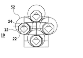
また、撮像面18において、各受光部12ごとに光学系の一部をなすマイクロレンズ52を備えている。このマイクロレンズ52は、撮像面18への入射光を各画素ごとに効率よく集光して受光部12の開口部に入射するものである。この集光によって、受光部12の開口率は実質的に向上する。マイクロレンズ52は、受光部12を覆うようにして、通常では、その光学中心を受光部12の開口部の中心に合わせて設置されるが、本実施例では、撮像面18の周縁部に位置する受光部12においては、図6に示すように、その光学中心を従感光部24の側に寄せて設置されている。
【0023】
固体撮像素子10は、たとえばディジタルスチルカメラなどの固体撮像装置に適用されて、入射光による被写界像を撮像面18に結像する。この固体撮像装置では、図3に示すように、入射光を光学系レンズ34により集光して撮像面18に照射するとよい。
【0024】
このとき、撮像面18では、入射光は、画素ごとに画像信号が得られるように、マイクロレンズ52によってさらに集光され、各画素に対応する受光部12に入射する。入射光は、受光部12においてカラーフィルタR、GまたはBを透過して、主感光部22および従感光部24に入射し、これらの感光部において、光電変換により各色の信号電荷が生成される。
【0025】
本実施例では、図6に示すように、マイクロレンズ52の光学中心を従感光部24の側に寄せて設置している。このため、従感光部24が主感光部22の同図における上方に設置されていると、特に撮像面18の下側では、図11に示すように、斜めに入射する入射光604がマイクロレンズ52によって効率よく集光され、主感光部の開口部62だけでなく従感光部の開口部64においても、集光されて入射する光束が増加する。このとき、撮像面18の中心部付近および上側では、マイクロレンズ52の光学中心を受光部12の開口部の中心にほとんど合わせても各感光部22および24の集光率は高いので、マイクロレンズ52を寄せる量は少なくてよい。
【0026】
このように、本発明の固体撮像素子10は、撮像面18の各受光部12において、従感光部24が主感光部22に対して一方の側に設置されているとき、マイクロレンズ52の光学中心を従感光部24の側に寄せて設置することによって、各感光部22および24の集光率を向上させている。このとき、受光部12の画素位置が撮像面18の中心部から周縁部に近づくほどマイクロレンズ52を寄せる距離を長くして設置してもよい。また、受光部12が撮像面18の中心部付近にあるとき、または受光部12において、従感光部24が主感光部22に対して撮像面18の周縁部側に設置されているときには、マイクロレンズ52を寄せる量は少なくてよい。このように、特に集光率の低下しやすい位置にある受光部12において、マイクロレンズ52が撮像面18の中心寄りにずらして設置され、集光率を向上させている。
【0027】
さらに、マイクロレンズ52を寄せる際に、マイクロレンズ52の光学中心を従感光部24の中心に合わせて設置してもよい。また、各受光部12において、主感光部22を撮像面18の中心部に近い側に、また従感光部24を撮像面18の中心部から遠い側に配置して、たとえば従感光部24を主感光部22に対して左右上下のいずれかの位置に配置してもよい。
【0028】
たとえば、この撮像面18の平面における上側では、従感光部24を主感光部22の下方に、また撮像面18の下側では、従感光部24を主感光部22の上方に配置すると、マイクロレンズ52および従感光部24が撮像面18の中心に対して上下に均等に配置され、撮像面18の上側と下側とで集光率に差が生じるのを防ぐことができる。他方、各受光部12において、従感光部24を主感光部22に対して撮像面18の周縁部側に配置すると、マイクロレンズ52および従感光部24が撮像面18の中心に対して同心状に配置され、撮像面18の全面において集光率を向上させることができる。
【0029】
また、他の実施例として、固体撮像素子10は、撮像面18の周縁部に位置する受光部12において、マイクロレンズ52を撮像面18の中心方向にずらして設置し、これによって、撮像面18の周縁部に発生する感度低下およびシェーディングを低減する。
【0030】
たとえば、図7に示すように、撮像面18の中心部付近の受光部12では、マイクロレンズ52をほとんどずらさずに設置し、撮像面18の周縁部の受光部12では、マイクロレンズ52を矢印 702の方向に、すなわちマイクロレンズ52の中心を受光部12の開口部の中心から撮像面18の中心方向にずらして設置する。これによって、たとえば、撮像面18の平面における上側および下側の受光部12では、それぞれ図12および図13に示すように、斜めの入射光604をマイクロレンズ52により都合よく集光し、主感光部の開口部62、および従感光部の開口部64に効率よく入射して、集光率を向上することができる。
【0031】
このとき、各受光部12において、従感光部24が主感光部22の上方に設置されるときには、このマイクロレンズ52は、撮像面18の下側に位置する受光部12では、上側に位置する受光部12よりも、大きくずらして設置してもよい。図7では、矢印の長さがこのずらし量を概念的に示している。これによって、撮像面18の上側と下側とで集光率に差が生じるのを防ぐことができる。
【0032】
また、受光部12が撮像面18の中心部から周縁部に近づくほど、マイクロレンズ52を大きくずらすように設置してもよい。これによって、斜めの入射光604が各受光部12に与える影響の大きさに応じて、集光率を向上させ、撮像面18の全面において、各受光部12の受光光量を均一にすることができる。
【0033】
このように、各受光部12に備えられているマイクロレンズ52をずらして設置することにより、有利には、マイクロレンズ52の中心を従感光部24の側に寄せて、またはマイクロレンズ52を撮像面18の中心方向にずらして設置することにより、特に撮像面18の周縁部において、主感光部22だけでなく従感光部18においても、このマイクロレンズ52により入射光を都合よく集光し、十分な受光光量を得ることができる。また、これによって各感光部22および24の感度低下、ならびに撮影した画像に発生するシェーディングを低減することができる。
【0034】
【発明の効果】
このように本発明によれば、固体撮像素子は、その撮像面に、感度の異なる複数の感光部で形成した受光部を画素として配列してダイナミックレンジを拡大する場合に、その受光部の中心からマイクロレンズの光学中心をずらして設置することにより、各受光部におけるマイクロレンズの集光率を向上させることができる。有利には、マイクロレンズの中心を従感光部の側に寄せて、またはマイクロレンズを撮像面の中心方向にずらして設置することにより、主感光部だけでなく従感光部においても十分な受光光量を得ることができる。これによって、特に従感光部の感度の低下およびばらつきを低減することができる。さらには、撮影した画像、特にその周縁部において発生するシェーディングを低減することができる。
【0035】
また、本発明による固体撮像素子は、マイクロレンズの設置によりシェーディングを補正しているため、固体撮像装置などに適用する際、補正回路などの処理部を省き、簡単な構成にすることができる。
【図面の簡単な説明】
【図1】本発明に係る固体撮像素子における撮像面の概略的な構成を示す平面図である。
【図2】図1に示す固体撮像素子の撮像面において、その一部を入射光の側から見た平面図である。
【図3】図1に示す固体撮像素子の撮像面において、光学系レンズが備えられた構成を示す説明的断面図である。
【図4】従来の固体撮像素子の撮像面において、受光部の開口部付近に出現する錯乱円を表した平面図である。
【図5】マイクロレンズを備えた従来の固体撮像素子において、その撮像面の一部を入射光の側から見た平面図である。
【図6】マイクロレンズを備えた本実施例の固体撮像素子において、その撮像面の一部を入射光の側から見た平面図である。
【図7】固体撮像素子の撮像面において、各受光部のマイクロレンズをずらす方向および量を表した平面図である。
【図8】従来の固体撮像素子の撮像面において、入射光が垂直に入射するとき、マイクロレンズが備えられた受光部の説明的断面図である。
【図9】従来の固体撮像素子の撮像面の上側において、マイクロレンズが備えられた受光部の説明的断面図である。
【図10】従来の固体撮像素子の撮像面の下側において、マイクロレンズが備えられた受光部の説明的断面図である。
【図11】図1の固体撮像素子の撮像面の下側において、マイクロレンズの中心を従感光部の側に寄せて備えられた受光部の説明的断面図である。
【図12】固体撮像素子の撮像面の上側において、撮像面の中心方向にマイクロレンズをずらして備えられた受光部の説明的断面図である。
【図13】固体撮像素子の撮像面の下側において、撮像面の中心方向にマイクロレンズをずらして備えられた受光部の説明的断面図である。
【符号の説明】
10 固体撮像素子
12 受光部
14 垂直転送部
16 水平転送部
18 撮像面[0001]
BACKGROUND OF THE INVENTION
The present invention provides a light receiving unit in which a plurality of photosensitive units having different sensitivities are arranged in each pixel on an imaging surface on which incident light from an object field is incident, and a microlens that collects incident light on the light receiving unit. The present invention relates to a solid-state imaging device provided.
[0002]
[Prior art]
Conventionally, solid-state imaging devices have a wide dynamic range by providing a sensitivity difference by forming a primary photosensitive portion and a secondary photosensitive portion with different aperture sizes in the light receiving portion corresponding to each pixel. Yes. At this time, the main photosensitive portion is a photosensitive portion having a large opening and high sensitivity, and an incident light quantity exceeding a certain level cannot be specified, but the secondary photosensitive portion is a photosensitive portion having a small opening and low sensitivity. Therefore, it is difficult to saturate as compared with the main photosensitive portion, so that an appropriate amount of incident light can be obtained. Therefore, an image signal is obtained in a wide dynamic range by mixing the signal outputs of these photosensitive portions for each pixel.
[0003]
By the way, in the image signal output from the solid-state imaging device, shading occurs in which the amount of received light in each light receiving unit is non-uniform due to various causes. In the case of a digital camera using a solid-state imaging device on which a microlens is formed, incident light is condensed by the microlens and incident on the light receiving unit, so the aperture ratio is substantially improved. The amount of light received by each light receiving unit varies. In general, a large amount of incident light is incident on the peripheral edge of the solid-state imaging device, and the direction of the inclination is biased. Therefore, the amount of light received at the light receiving portion is lower than that at the center. For this reason, so-called shading occurs in which luminance decreases at the peripheral edge of the captured image. Conventionally, an image signal in which shading has occurred is corrected by using digital processing or a memory, and the correction circuit can be simplified.
[0004]
However, in a solid-state imaging device, when a plurality of photosensitive parts having different sensitivities are formed in the light receiving part corresponding to the pixel to increase the dynamic range, the photoelectric conversion characteristics and the like differ from one photosensitive part to another. Can not. Therefore, in order to perform this appropriate shading correction, in Patent Document 1, a light-receiving element with low sensitivity (that is, the above-described photosensitive portion) is arranged on the side far from the center of the imaging screen in each pixel. By providing a solid-state imaging device that is arranged symmetrically with respect to the center of the screen as a whole at any position on the left, right, top, and bottom with respect to the light receiving element with high sensitivity in the light receiving unit, shading bias is prevented and the sensitivity differs. A solid-state imaging device that performs a common shading correction on a light receiving element is also known.
[0005]
[Patent Document 1]
Japanese Patent Application No. 2002-228562.
[0006]
[Problems to be solved by the invention]
When the solid-state imaging device described above is applied to a solid-state imaging device such as a digital still camera, the
[0007]
As shown in FIG. 5, the
[0008]
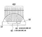
For example, as shown in FIG. 8,
[0009]
As described above, in the
[0010]
In addition, when incident light forms an image on the
[0011]
In the
[0012]
The present invention eliminates such disadvantages of the prior art, particularly reduces the decrease in sensitivity in a low-sensitivity photosensitive portion, and further reduces shading that occurs on the imaging surface, particularly in the peripheral portion thereof, to prevent deterioration in image quality. It is an object of the present invention to provide a solid-state imaging device that can be used.
[0013]
[Means for Solving the Problems]
According to the present invention, the image pickup surface includes an image pickup surface that forms incident light from the object scene, and the image pickup surface is arranged in the row and column directions, and a plurality of light receiving units corresponding to the respective pixels forming the image pickup surface, And a microlens that is provided in each of the plurality of light receiving units and collects incident light, and each of the plurality of light receiving units has a first sensitivity and photoelectrically converts the incident light. In the solid-state imaging device including the photosensitive portion and the second photosensitive portion having a second sensitivity lower than the first sensitivity and photoelectrically converting the incident light, the microlens has its optical center at the optical center. The center of the image pickup surface is shifted from the center of the image pickup surface.
[0014]
DETAILED DESCRIPTION OF THE INVENTION
Next, embodiments of a solid-state imaging device according to the present invention will be described in detail with reference to the accompanying drawings.
[0015]
In the solid-state imaging device of the embodiment, the light receiving unit corresponding to the pixel uses a plurality of photosensitive units to change the size of the opening of each photosensitive unit, thereby changing sensitivity, that is, photoelectric conversion efficiency, and dynamically We are trying to expand the range. The center of the microlens that collects light to the opening of the photosensitive part is conveniently arranged so as to be shifted from the center of the light-receiving part, so that the photosensitive part, particularly the low-sensitivity photosensitive part, particularly at the periphery of the imaging surface. The light condensing rate is improved, and the sensitivity reduction and luminance shading in the light receiving portion are reduced to prevent the image quality from being deteriorated.
[0016]
As shown in FIG. 1, the solid-
[0017]
The
[0018]
In this embodiment, as shown in FIG. 1, the
[0019]
The
[0020]
The main
[0021]
The vertical transfer path (VCCD) 14 is installed so as to sew each light receiving portion in a zigzag shape in the vertical direction. The vertical transfer path 14 is a charge coupled device, and is formed adjacent to the area covered by the light shielding member 26 according to the shapes of the main
[0022]
In addition, the
[0023]
The solid-
[0024]
At this time, on the
[0025]
In this embodiment, as shown in FIG. 6, the optical center of the
[0026]
As described above, in the solid-
[0027]
Further, when the
[0028]
For example, if the secondary
[0029]
As another embodiment, the solid-
[0030]
For example, as shown in FIG. 7, in the
[0031]
At this time, in each light receiving
[0032]
Further, the
[0033]
As described above, by shifting the
[0034]
【The invention's effect】
As described above, according to the present invention, when the solid-state imaging device is arranged on the imaging surface with a light receiving portion formed of a plurality of photosensitive portions having different sensitivities as pixels to expand the dynamic range, the center of the light receiving portion is arranged. Since the optical centers of the microlenses are shifted from each other, the condensing rate of the microlenses in each light receiving unit can be improved. Advantageously, the center of the microlens is moved to the side of the secondary photosensitive unit, or the microlens is shifted in the direction of the center of the imaging surface, so that a sufficient amount of received light is received not only in the primary photosensitive unit but also in the secondary photosensitive unit. Can be obtained. As a result, it is possible to reduce the decrease and variation in the sensitivity of the secondary photosensitive portion. Furthermore, it is possible to reduce shading that occurs at the captured image, particularly at the peripheral edge thereof.
[0035]
In addition, since the solid-state imaging device according to the present invention corrects shading by installing a microlens, when applied to a solid-state imaging device or the like, a processing unit such as a correction circuit can be omitted and the configuration can be simplified.
[Brief description of the drawings]
FIG. 1 is a plan view showing a schematic configuration of an imaging surface in a solid-state imaging device according to the present invention.
2 is a plan view of a part of the imaging surface of the solid-state imaging device shown in FIG. 1 as viewed from the incident light side.
3 is an explanatory cross-sectional view showing a configuration in which an optical system lens is provided on the imaging surface of the solid-state imaging device shown in FIG. 1;
FIG. 4 is a plan view showing a circle of confusion that appears in the vicinity of an opening of a light receiving unit on an imaging surface of a conventional solid-state imaging device.
FIG. 5 is a plan view of a part of an imaging surface of a conventional solid-state imaging device including a microlens as viewed from an incident light side.
FIG. 6 is a plan view of a part of the imaging surface of the solid-state imaging device according to the present embodiment including a microlens as viewed from the incident light side.
FIG. 7 is a plan view showing the direction and amount of shifting the microlens of each light receiving unit on the imaging surface of the solid-state imaging device.
FIG. 8 is an explanatory cross-sectional view of a light receiving unit provided with a microlens when incident light is vertically incident on an imaging surface of a conventional solid-state imaging device.
FIG. 9 is an explanatory cross-sectional view of a light receiving unit provided with a microlens above the imaging surface of a conventional solid-state imaging device.
FIG. 10 is an explanatory cross-sectional view of a light receiving unit provided with a microlens below the imaging surface of a conventional solid-state imaging device.
11 is an explanatory cross-sectional view of a light receiving unit provided below the imaging surface of the solid-state imaging device in FIG. 1 with the center of the microlens being moved toward the secondary photosensitive unit.
FIG. 12 is an explanatory cross-sectional view of a light receiving unit provided on the upper side of the imaging surface of the solid-state imaging device by shifting the microlens toward the center of the imaging surface.
FIG. 13 is an explanatory cross-sectional view of a light receiving unit provided on the lower side of the imaging surface of the solid-state imaging device by shifting the microlens toward the center of the imaging surface.
[Explanation of symbols]
DESCRIPTION OF
Claims (6)
該撮像面は、行および列方向に配列され該撮像面を形成する各画素に対応する複数の受光部、および該複数の受光部のそれぞれに備えられて入射光を集光するマイクロレンズを含み、
前記複数の受光部のそれぞれは、第1の感度を有し、前記入射光を光電変換する第1の感光部と、第1の感度より低い第2の感度を有し、前記入射光を光電変換する第2の感光部とを含む固体撮像素子において、
前記マイクロレンズは、その光学中心を前記受光部の中心から前記撮像面の中心寄りにずらして設置されていることを特徴とする固体撮像素子。Including an imaging surface that images incident light from the object scene,
The imaging surface includes a plurality of light receiving portions corresponding to each pixel arranged in the row and column directions and corresponding to each pixel, and a microlens that is provided in each of the plurality of light receiving portions and collects incident light. ,
Each of the plurality of light receiving units has a first sensitivity, a first photosensitive unit that photoelectrically converts the incident light, and a second sensitivity that is lower than the first sensitivity. In a solid-state imaging device including a second photosensitive portion to be converted,
The solid-state imaging device, wherein the microlens is installed with its optical center shifted from the center of the light receiving unit toward the center of the imaging surface.
第2の感光部が第1の感光部に対して前記撮像面の中心部側に位置する受光部について、前記マイクロレンズは、その光学中心を前記受光部の第2の感光部の側に寄せて設置されていることを特徴とする固体撮像素子。4. The solid-state imaging device according to claim 1, wherein the second photosensitive portion is disposed on one side with respect to the first photosensitive portion,
With respect to the light receiving unit in which the second photosensitive unit is located on the center side of the imaging surface with respect to the first photosensitive unit, the microlens brings its optical center closer to the second photosensitive unit side of the light receiving unit. A solid-state imaging device characterized by being installed.
Priority Applications (5)
| Application Number | Priority Date | Filing Date | Title |
|---|---|---|---|
| JP2002323859A JP4136611B2 (en) | 2002-11-07 | 2002-11-07 | Solid-state image sensor |
| US10/698,393 US7019279B2 (en) | 2002-11-07 | 2003-11-03 | Solid-state image sensor with the optical center of microlenses shifted from the center of photo-sensors for increasing the convergence ratio |
| TW092131022A TWI235606B (en) | 2002-11-07 | 2003-11-06 | Solid state image pick up device |
| KR1020030078723A KR100572228B1 (en) | 2002-11-07 | 2003-11-07 | Solid state imaging device |
| CNB2003101132353A CN1245828C (en) | 2002-11-07 | 2003-11-07 | Solid pick-up element |
Applications Claiming Priority (1)
| Application Number | Priority Date | Filing Date | Title |
|---|---|---|---|
| JP2002323859A JP4136611B2 (en) | 2002-11-07 | 2002-11-07 | Solid-state image sensor |
Publications (2)
| Publication Number | Publication Date |
|---|---|
| JP2004158686A true JP2004158686A (en) | 2004-06-03 |
| JP4136611B2 JP4136611B2 (en) | 2008-08-20 |
Family
ID=32211923
Family Applications (1)
| Application Number | Title | Priority Date | Filing Date |
|---|---|---|---|
| JP2002323859A Expired - Fee Related JP4136611B2 (en) | 2002-11-07 | 2002-11-07 | Solid-state image sensor |
Country Status (5)
| Country | Link |
|---|---|
| US (1) | US7019279B2 (en) |
| JP (1) | JP4136611B2 (en) |
| KR (1) | KR100572228B1 (en) |
| CN (1) | CN1245828C (en) |
| TW (1) | TWI235606B (en) |
Cited By (3)
| Publication number | Priority date | Publication date | Assignee | Title |
|---|---|---|---|---|
| KR100712348B1 (en) * | 2005-09-12 | 2007-05-02 | 매그나칩 반도체 유한회사 | Image sensor with decreased optical interference between adjacent pixel |
| US7598581B2 (en) | 2005-09-12 | 2009-10-06 | Crosstek Capital, LLC | Image sensor with decreased optical interference between adjacent pixels |
| US7839366B2 (en) | 2005-11-14 | 2010-11-23 | Samsung Electronics Co., Ltd. | Display device |
Families Citing this family (14)
| Publication number | Priority date | Publication date | Assignee | Title |
|---|---|---|---|---|
| US7423679B2 (en) * | 2002-12-20 | 2008-09-09 | Eastman Kodak Company | Imaging system having extended useful latitude |
| US6903391B2 (en) * | 2003-09-10 | 2005-06-07 | Fuji Photo Film Co., Ltd. | Solid state image pickup device |
| TWI236546B (en) * | 2004-04-15 | 2005-07-21 | Pixart Imaging Inc | Image sensing device of improving image quality and reducing color shift effect |
| JP4469732B2 (en) * | 2004-05-07 | 2010-05-26 | 富士フイルム株式会社 | Solid-state image sensor |
| US7564629B1 (en) | 2004-12-02 | 2009-07-21 | Crosstek Capital, LLC | Microlens alignment procedures in CMOS image sensor design |
| US7450161B1 (en) | 2004-12-02 | 2008-11-11 | Magnachip Semiconductor Ltd. | System and method to enhance the uniformity of intensity distribution on digital imaging sensors |
| US7763918B1 (en) * | 2004-12-02 | 2010-07-27 | Chen Feng | Image pixel design to enhance the uniformity of intensity distribution on digital image sensors |
| JP2006246130A (en) * | 2005-03-04 | 2006-09-14 | Konica Minolta Photo Imaging Inc | Imaging system, interchangeable lens, imaging apparatus, and ic tag |
| JP4456040B2 (en) * | 2005-06-17 | 2010-04-28 | パナソニック株式会社 | Solid-state image sensor |
| JP5277565B2 (en) * | 2007-05-31 | 2013-08-28 | 富士通セミコンダクター株式会社 | Solid-state image sensor |
| US8648948B2 (en) * | 2009-09-30 | 2014-02-11 | Infrared Newco, Inc. | Imaging systems with multiple imaging pixel types and related methods |
| CN106571106A (en) * | 2015-10-10 | 2017-04-19 | 卢琳庆 | Display technology for colors with RGB arrayed in hexagons for color image display |
| EP3171406B1 (en) * | 2015-11-23 | 2019-06-19 | ams AG | Photodiode array |
| CN113046544B (en) * | 2021-02-23 | 2022-07-15 | 首钢京唐钢铁联合有限责任公司 | Air-fuel ratio control method and control system for continuous annealing furnace |
Family Cites Families (5)
| Publication number | Priority date | Publication date | Assignee | Title |
|---|---|---|---|---|
| JPH08107194A (en) * | 1994-10-03 | 1996-04-23 | Fuji Photo Optical Co Ltd | Solid state image sensor |
| JP4018820B2 (en) * | 1998-10-12 | 2007-12-05 | 富士フイルム株式会社 | Solid-state imaging device and signal readout method |
| JP3943273B2 (en) * | 1999-01-28 | 2007-07-11 | 富士フイルム株式会社 | Solid-state imaging device and signal readout method |
| US6777661B2 (en) * | 2002-03-15 | 2004-08-17 | Eastman Kodak Company | Interlined charge-coupled device having an extended dynamic range |
| JP4034614B2 (en) * | 2002-08-06 | 2008-01-16 | 富士フイルム株式会社 | Solid-state imaging device |
-
2002
- 2002-11-07 JP JP2002323859A patent/JP4136611B2/en not_active Expired - Fee Related
-
2003
- 2003-11-03 US US10/698,393 patent/US7019279B2/en not_active Expired - Lifetime
- 2003-11-06 TW TW092131022A patent/TWI235606B/en not_active IP Right Cessation
- 2003-11-07 CN CNB2003101132353A patent/CN1245828C/en not_active Expired - Fee Related
- 2003-11-07 KR KR1020030078723A patent/KR100572228B1/en active IP Right Grant
Cited By (5)
| Publication number | Priority date | Publication date | Assignee | Title |
|---|---|---|---|---|
| KR100712348B1 (en) * | 2005-09-12 | 2007-05-02 | 매그나칩 반도체 유한회사 | Image sensor with decreased optical interference between adjacent pixel |
| US7598581B2 (en) | 2005-09-12 | 2009-10-06 | Crosstek Capital, LLC | Image sensor with decreased optical interference between adjacent pixels |
| US8030723B2 (en) | 2005-09-12 | 2011-10-04 | Crosstek Capital, LLC | Image sensor with decreased optical interference between adjacent pixels |
| US8698266B2 (en) | 2005-09-12 | 2014-04-15 | Intellectual Ventures Ii Llc | Image sensor with decreased optical interference between adjacent pixels |
| US7839366B2 (en) | 2005-11-14 | 2010-11-23 | Samsung Electronics Co., Ltd. | Display device |
Also Published As
| Publication number | Publication date |
|---|---|
| US20040089788A1 (en) | 2004-05-13 |
| CN1245828C (en) | 2006-03-15 |
| US7019279B2 (en) | 2006-03-28 |
| TWI235606B (en) | 2005-07-01 |
| TW200425726A (en) | 2004-11-16 |
| KR100572228B1 (en) | 2006-04-19 |
| KR20040041066A (en) | 2004-05-13 |
| CN1499832A (en) | 2004-05-26 |
| JP4136611B2 (en) | 2008-08-20 |
Similar Documents
| Publication | Publication Date | Title |
|---|---|---|
| JP4018820B2 (en) | Solid-state imaging device and signal readout method | |
| JP4136611B2 (en) | Solid-state image sensor | |
| JP4421793B2 (en) | Digital camera | |
| JP4241840B2 (en) | Imaging device | |
| US8466998B2 (en) | Solid-state image sensor and imaging apparatus equipped with solid-state image sensor | |
| TWI508270B (en) | Image sensor having multiple sensing layers | |
| JP4291793B2 (en) | Solid-state imaging device and solid-state imaging device | |
| JP2007155929A (en) | Solid-state imaging element and imaging apparatus using the same | |
| JP4920839B2 (en) | Imaging device | |
| JP2009004615A (en) | Back irradiation image sensor | |
| WO2020012860A1 (en) | Imaging element and method for manufacturing imaging element | |
| JP3571982B2 (en) | Solid-state imaging device and solid-state imaging system having the same | |
| JP2006270364A (en) | Solid-state image pickup element and solid-state image pickup device, and driving method thereof | |
| EP1351311A2 (en) | An interlined charge-coupled device having an extended dynamic range | |
| JP4264248B2 (en) | Color solid-state imaging device | |
| JPH0750401A (en) | Solid state image pick-up device and manufacturing method thereof | |
| JP4264249B2 (en) | MOS type image sensor and digital camera | |
| JP2007066962A (en) | Color solid-state imaging device and digital camera | |
| JPH0637289A (en) | Solid-state image sensing device | |
| JP4758160B2 (en) | Solid-state imaging device and driving method thereof | |
| JP4909965B2 (en) | Imaging device | |
| JP2000125311A (en) | Solid-state image pickup device | |
| JP2010153603A (en) | Solid state imaging apparatus | |
| JP7381067B2 (en) | Imaging device and imaging device | |
| JPS63147365A (en) | Solid-state image sensing device |
Legal Events
| Date | Code | Title | Description |
|---|---|---|---|
| A621 | Written request for application examination |
Free format text: JAPANESE INTERMEDIATE CODE: A621 Effective date: 20050302 |
|
| A711 | Notification of change in applicant |
Free format text: JAPANESE INTERMEDIATE CODE: A712 Effective date: 20061207 |
|
| A977 | Report on retrieval |
Free format text: JAPANESE INTERMEDIATE CODE: A971007 Effective date: 20070606 |
|
| A131 | Notification of reasons for refusal |
Free format text: JAPANESE INTERMEDIATE CODE: A131 Effective date: 20070612 |
|
| A521 | Request for written amendment filed |
Free format text: JAPANESE INTERMEDIATE CODE: A523 Effective date: 20070809 |
|
| A521 | Request for written amendment filed |
Free format text: JAPANESE INTERMEDIATE CODE: A523 Effective date: 20070810 |
|
| A02 | Decision of refusal |
Free format text: JAPANESE INTERMEDIATE CODE: A02 Effective date: 20071002 |
|
| A521 | Request for written amendment filed |
Free format text: JAPANESE INTERMEDIATE CODE: A523 Effective date: 20071026 |
|
| A911 | Transfer to examiner for re-examination before appeal (zenchi) |
Free format text: JAPANESE INTERMEDIATE CODE: A911 Effective date: 20071213 |
|
| A131 | Notification of reasons for refusal |
Free format text: JAPANESE INTERMEDIATE CODE: A131 Effective date: 20080129 |
|
| A521 | Request for written amendment filed |
Free format text: JAPANESE INTERMEDIATE CODE: A523 Effective date: 20080321 |
|
| TRDD | Decision of grant or rejection written | ||
| A01 | Written decision to grant a patent or to grant a registration (utility model) |
Free format text: JAPANESE INTERMEDIATE CODE: A01 Effective date: 20080507 |
|
| A01 | Written decision to grant a patent or to grant a registration (utility model) |
Free format text: JAPANESE INTERMEDIATE CODE: A01 |
|
| A61 | First payment of annual fees (during grant procedure) |
Free format text: JAPANESE INTERMEDIATE CODE: A61 Effective date: 20080603 |
|
| R150 | Certificate of patent or registration of utility model |
Ref document number: 4136611 Country of ref document: JP Free format text: JAPANESE INTERMEDIATE CODE: R150 Free format text: JAPANESE INTERMEDIATE CODE: R150 |
|
| FPAY | Renewal fee payment (event date is renewal date of database) |
Free format text: PAYMENT UNTIL: 20110613 Year of fee payment: 3 |
|
| FPAY | Renewal fee payment (event date is renewal date of database) |
Free format text: PAYMENT UNTIL: 20110613 Year of fee payment: 3 |
|
| FPAY | Renewal fee payment (event date is renewal date of database) |
Free format text: PAYMENT UNTIL: 20120613 Year of fee payment: 4 |
|
| R250 | Receipt of annual fees |
Free format text: JAPANESE INTERMEDIATE CODE: R250 |
|
| FPAY | Renewal fee payment (event date is renewal date of database) |
Free format text: PAYMENT UNTIL: 20120613 Year of fee payment: 4 |
|
| FPAY | Renewal fee payment (event date is renewal date of database) |
Free format text: PAYMENT UNTIL: 20130613 Year of fee payment: 5 |
|
| R250 | Receipt of annual fees |
Free format text: JAPANESE INTERMEDIATE CODE: R250 |
|
| R250 | Receipt of annual fees |
Free format text: JAPANESE INTERMEDIATE CODE: R250 |
|
| S111 | Request for change of ownership or part of ownership |
Free format text: JAPANESE INTERMEDIATE CODE: R313113 |
|
| R350 | Written notification of registration of transfer |
Free format text: JAPANESE INTERMEDIATE CODE: R350 |
|
| R250 | Receipt of annual fees |
Free format text: JAPANESE INTERMEDIATE CODE: R250 |
|
| R250 | Receipt of annual fees |
Free format text: JAPANESE INTERMEDIATE CODE: R250 |
|
| R250 | Receipt of annual fees |
Free format text: JAPANESE INTERMEDIATE CODE: R250 |
|
| R250 | Receipt of annual fees |
Free format text: JAPANESE INTERMEDIATE CODE: R250 |
|
| R250 | Receipt of annual fees |
Free format text: JAPANESE INTERMEDIATE CODE: R250 |
|
| R250 | Receipt of annual fees |
Free format text: JAPANESE INTERMEDIATE CODE: R250 |
|
| R250 | Receipt of annual fees |
Free format text: JAPANESE INTERMEDIATE CODE: R250 |
|
| R250 | Receipt of annual fees |
Free format text: JAPANESE INTERMEDIATE CODE: R250 |
|
| LAPS | Cancellation because of no payment of annual fees |