JP2004147323A - Heterodyne-based optical spectrum analysis of using controlled optical attenuation - Google Patents
Heterodyne-based optical spectrum analysis of using controlled optical attenuation Download PDFInfo
- Publication number
- JP2004147323A JP2004147323A JP2003360135A JP2003360135A JP2004147323A JP 2004147323 A JP2004147323 A JP 2004147323A JP 2003360135 A JP2003360135 A JP 2003360135A JP 2003360135 A JP2003360135 A JP 2003360135A JP 2004147323 A JP2004147323 A JP 2004147323A
- Authority
- JP
- Japan
- Prior art keywords
- signal
- input signal
- optical
- attenuation level
- attenuation
- Prior art date
- Legal status (The legal status is an assumption and is not a legal conclusion. Google has not performed a legal analysis and makes no representation as to the accuracy of the status listed.)
- Pending
Links
- 230000003287 optical effect Effects 0.000 title claims abstract description 143
- 238000010183 spectrum analysis Methods 0.000 title description 3
- 238000001514 detection method Methods 0.000 claims abstract description 56
- 230000004044 response Effects 0.000 claims abstract description 28
- 238000005259 measurement Methods 0.000 claims description 62
- 238000000034 method Methods 0.000 claims description 39
- 238000006467 substitution reaction Methods 0.000 claims 1
- 229920006395 saturated elastomer Polymers 0.000 abstract description 10
- 239000000835 fiber Substances 0.000 description 16
- 238000010586 diagram Methods 0.000 description 15
- 230000002238 attenuated effect Effects 0.000 description 10
- 238000001228 spectrum Methods 0.000 description 9
- 239000013307 optical fiber Substances 0.000 description 6
- 230000001427 coherent effect Effects 0.000 description 4
- 238000012545 processing Methods 0.000 description 4
- 230000005540 biological transmission Effects 0.000 description 3
- 230000003321 amplification Effects 0.000 description 2
- 230000000903 blocking effect Effects 0.000 description 2
- 239000006185 dispersion Substances 0.000 description 2
- 238000003199 nucleic acid amplification method Methods 0.000 description 2
- 230000003595 spectral effect Effects 0.000 description 2
- 238000004364 calculation method Methods 0.000 description 1
- 238000004891 communication Methods 0.000 description 1
- 238000013016 damping Methods 0.000 description 1
- 238000001914 filtration Methods 0.000 description 1
- 239000000203 mixture Substances 0.000 description 1
- 238000012544 monitoring process Methods 0.000 description 1
- 238000003012 network analysis Methods 0.000 description 1
- 230000007935 neutral effect Effects 0.000 description 1
- 230000000737 periodic effect Effects 0.000 description 1
- 230000010287 polarization Effects 0.000 description 1
- 230000004043 responsiveness Effects 0.000 description 1
- 238000009738 saturating Methods 0.000 description 1
- 230000035945 sensitivity Effects 0.000 description 1
Images


Classifications
-
- G—PHYSICS
- G01—MEASURING; TESTING
- G01J—MEASUREMENT OF INTENSITY, VELOCITY, SPECTRAL CONTENT, POLARISATION, PHASE OR PULSE CHARACTERISTICS OF INFRARED, VISIBLE OR ULTRAVIOLET LIGHT; COLORIMETRY; RADIATION PYROMETRY
- G01J9/00—Measuring optical phase difference; Determining degree of coherence; Measuring optical wavelength
- G01J9/04—Measuring optical phase difference; Determining degree of coherence; Measuring optical wavelength by beating two waves of a same source but of different frequency and measuring the phase shift of the lower frequency obtained
-
- G—PHYSICS
- G01—MEASURING; TESTING
- G01J—MEASUREMENT OF INTENSITY, VELOCITY, SPECTRAL CONTENT, POLARISATION, PHASE OR PULSE CHARACTERISTICS OF INFRARED, VISIBLE OR ULTRAVIOLET LIGHT; COLORIMETRY; RADIATION PYROMETRY
- G01J1/00—Photometry, e.g. photographic exposure meter
- G01J1/02—Details
- G01J2001/0276—Protection
Abstract
Description
本発明は、概して光学的測定及び測定システムの分野に関し、より詳細には光ヘテロダイン検出を利用する光スペクトル分析のための方法及びシステムに関する。 The present invention relates generally to the field of optical measurement and measurement systems, and more particularly to methods and systems for optical spectrum analysis utilizing optical heterodyne detection.
本出願は、2000年1月20日に出願された特許文献1に関連する。
{This application is related to
光ヘテロダイン検出システムは、高スペクトル解像度を達成するその能力の故に、DWDM(高密度波長分割多重)システムをモニタするために利用されている。感度及びダイナミックレンジといったパラメータに関する光ヘテロダイン検出システムの性能の改善は、ヘテロダインビート信号の信号対雑音比を増やすことにより達成され得る。しかしながら、所望のヘテロダインビート信号は他の直接検出信号と共存する。DWDMシステムの直接検出信号には、入力信号と局部発振器信号の両方からの強度雑音及びショット雑音が含まれる。様々な雑音成分は、所望のヘテロダインビート信号をマスキングする可能性がある。ヘテロダインビート信号の信号対雑音比を改善するための一つの技術には、二つの検出器を利用して平衡検出を達成することにより強度雑音を低減することが含まれる。平衡検出はヘテロダインビート信号の信号対雑音比を改善することに役立つが、平衡検出には限界がある。 Optical heterodyne detection systems have been used to monitor DWDM (Dense Wavelength Division Multiplexing) systems because of their ability to achieve high spectral resolution. Improving the performance of an optical heterodyne detection system with respect to parameters such as sensitivity and dynamic range can be achieved by increasing the signal-to-noise ratio of the heterodyne beat signal. However, the desired heterodyne beat signal coexists with other direct detection signals. The direct detection signal of a DWDM system includes intensity noise and shot noise from both the input signal and the local oscillator signal. Various noise components can mask the desired heterodyne beat signal. One technique for improving the signal-to-noise ratio of a heterodyne beat signal involves reducing intensity noise by using two detectors to achieve balanced detection. While balanced detection helps improve the signal-to-noise ratio of the heterodyne beat signal, balanced detection has its limitations.
ヘテロダインビート信号の信号対雑音比を改善するための別の技術には、ヘテロダインビート信号の振幅を増大させ、それによってヘテロダインビート信号の信号対雑音比を高めるように、入力信号を局部発振器信号に合成する前に入力信号を増幅することが含まれる。入力信号の増幅はヘテロダインビート信号の振幅を増やすが、増幅は入力信号の強度雑音も増やし、ヘテロダイン信号の信号対雑音比を改善することができない。 Another technique for improving the signal-to-noise ratio of a heterodyne beat signal involves increasing the amplitude of the heterodyne beat signal, thereby increasing the signal-to-noise ratio of the heterodyne beat signal by converting the input signal to a local oscillator signal. Includes amplifying the input signal before combining. While amplification of the input signal increases the amplitude of the heterodyne beat signal, amplification also increases the intensity noise of the input signal and cannot improve the signal-to-noise ratio of the heterodyne signal.
光ヘテロダイン検出システムについての別の懸念は、受信器が光信号電力のサージに敏感であることである。例えば、光検出器は高信号電力にさらされると、飽和したり、又は永久的に損傷したりすることさえある。
既知のヘテロダイン検出システムの限界に鑑みて、高信号対雑音比でもってヘテロダインビート信号を生成する光ヘテロダイン検出システムが必要とされている。さらに、効果的に高信号電力のサージに対処することができる光ヘテロダイン検出システムが必要とされている。 In view of the limitations of known heterodyne detection systems, there is a need for an optical heterodyne detection system that generates a heterodyne beat signal with a high signal-to-noise ratio. Further, there is a need for an optical heterodyne detection system that can effectively cope with high signal power surges.
光ヘテロダイン検出システムは、入力信号を局部発振器信号と合成する前に、入力信号を減衰させるための減衰器を含む。本発明によれば、入力信号に関する最適減衰レベルが求められ、この最適減衰レベルによって、入力信号と局部発振器信号を合成した際に生成されるヘテロダインビート信号の信号対雑音比が改善される。また、本発明によれば、入力信号に関する最小減衰レベルが求められ、最小減衰レベルによって、受信器の光検出器が高電力信号により飽和したり又は損傷したりすることから保護される。 The optical heterodyne detection system includes an attenuator for attenuating the input signal before combining the input signal with the local oscillator signal. According to the present invention, an optimal attenuation level for an input signal is determined, and the optimal attenuation level improves the signal-to-noise ratio of a heterodyne beat signal generated when the input signal and the local oscillator signal are combined. Also, according to the present invention, a minimum attenuation level for the input signal is determined, which protects the photodetector of the receiver from being saturated or damaged by the high power signal.
本発明の他の態様及び利点は、一例として本発明の原理を例示する添付図面に関連してなされる、以下の詳細な説明から明らかとなろう。 Other aspects and advantages of the present invention will become apparent from the following detailed description, taken in conjunction with the accompanying drawings, illustrating by way of example the principles of the invention.
本発明によれば、入力信号に対する最適減衰レベルが求められ、この最適減衰レベルによって、入力信号と局部発振器信号を合成した際に生成されるヘテロダインビート信号の信号対雑音比が改善される。また、本発明によれば、入力信号に対する最小減衰レベルが求められ、この最小減衰レベルによって光検出器が高電力信号により飽和したり又は損傷したりすることから保護される。 According to the present invention, the optimum attenuation level for the input signal is determined, and the optimum attenuation level improves the signal-to-noise ratio of the heterodyne beat signal generated when the input signal and the local oscillator signal are combined. Also, according to the present invention, a minimum attenuation level for the input signal is determined, which protects the photodetector from being saturated or damaged by the high power signal.
光ヘテロダイン検出システムは、入力信号を局部発振器信号と合成する前に入力信号を減衰させるための減衰器を含む。本発明によれば、入力信号に対する最適減衰レベルが求められ、この最適減衰レベルによって、入力信号と局部発振器信号を合成した際に生成されるヘテロダインビート信号の信号対雑音比が改善される。また、本発明によれば、入力信号に対する最小減衰レベルが求められ、この最小減衰レベルによって光検出器が高電力信号により飽和したり又は損傷したりすることから保護される。 The optical heterodyne detection system includes an attenuator for attenuating the input signal before combining the input signal with the local oscillator signal. According to the present invention, an optimal attenuation level for an input signal is determined, and the optimal attenuation level improves a signal-to-noise ratio of a heterodyne beat signal generated when the input signal and the local oscillator signal are combined. Also, according to the present invention, a minimum attenuation level for the input signal is determined, which protects the photodetector from being saturated or damaged by the high power signal.
光ヘテロダイン検出分野において知られているように、入力信号と局部発振器信号を合成して、入力信号及び局部発振器信号からの強度雑音とショット雑音とヘテロダインビート信号を含む成分を有する光信号を生成する。入力信号の強度雑音が主雑音源である場合、入力信号を局部発振器信号と合成する前に入力信号を減衰させることにより、ヘテロダインビート信号の信号対雑音比を改善することができる。ヘテロダインビート信号の信号対雑音比が改善されるのは、入力信号とヘテロダインビート信号の強度雑音が入力信号の減衰でもって別々に変倍されるからである。具体的には、入力信号の強度雑音は入力信号の電力(PS)に比例する。入力信号の電力に対する入力信号強度雑音INの関係は、以下の通りである:
IN∝PS (1)
As is known in the field of optical heterodyne detection, an input signal and a local oscillator signal are combined to generate an optical signal having components including intensity noise, shot noise, and a heterodyne beat signal from the input signal and the local oscillator signal. . If the intensity noise of the input signal is the dominant noise source, the signal-to-noise ratio of the heterodyne beat signal can be improved by attenuating the input signal before combining the input signal with the local oscillator signal. The signal-to-noise ratio of the heterodyne beat signal is improved because the intensity noise of the input signal and the heterodyne beat signal are scaled separately with the attenuation of the input signal. Specifically, the intensity noise of the input signal is proportional to the input signal power (P S). Relationship between the input signal intensity noise I N for the input signal power is as follows:
I N αP S (1)
他方、ヘテロダインビート信号の強度は入力信号の電力PSの平方根に比例する。入力信号の電力に対するヘテロダイン信号の強度IHの関係は、以下の通りである:
IH∝√(PS) (2)
On the other hand, the strength of the heterodyne beat signal is proportional to the square root of the input signal power P S. The relationship of the intensity of the heterodyne signal I H to the power of the input signal is as follows:
I H α√ (P S) ( 2)
入力信号の強度雑音とヘテロダインビート信号との間の異なる変倍関係のために、入力信号の電力の減衰により入力信号の強度雑音はヘテロダインビート信号よりも速いレートで低下する。入力信号の強度雑音がヘテロダインビート信号よりも速いレートで低下するので、入力信号の強度雑音が主雑音源である場合にヘテロダインビート信号の信号対雑音比(IH/IN)は増加する。ヘテロダイン信号の信号対雑音比の増加により、入力信号の所望パラメータを特定するためのより良好な信号が提供され、それによって入力信号の強度雑音が主雑音源である場合に、検出性能が改善されることになる。ヘテロダインビート信号の信号対雑音比が入力信号の連続的な減衰とともに無限に増加しない点に留意されたい。入力信号の減衰が増加するにつれ、最終的に入力信号からの強度雑音以外の雑音成分(単数又は複数)が支配的となり、入力信号のさらなる減衰によって、ヘテロダインビート信号の信号対雑音比が低減される。例えば、或る時点で光受信器内の電気的雑音が入力信号の強度雑音にまさる主雑音源になる可能性がある。以下に詳細に説明される本発明の焦点には、最適減衰レベル(すなわち、信号対雑音比を最大化する減衰レベル)を求めることが含まれる。 Due to the different scaling relationship between the input signal intensity noise and the heterodyne beat signal, the input signal power attenuation causes the input signal intensity noise to drop at a faster rate than the heterodyne beat signal. The signal-to-noise ratio (I H / I N ) of the heterodyne beat signal increases when the intensity noise of the input signal is the main noise source because the intensity noise of the input signal drops at a faster rate than the heterodyne beat signal. Increasing the signal-to-noise ratio of the heterodyne signal provides a better signal for identifying desired parameters of the input signal, thereby improving detection performance when the input signal's intensity noise is the primary noise source. Will be. Note that the signal-to-noise ratio of the heterodyne beat signal does not increase infinitely with continuous attenuation of the input signal. As the attenuation of the input signal increases, eventually the noise component (s) other than the intensity noise from the input signal becomes dominant, and further attenuation of the input signal reduces the signal-to-noise ratio of the heterodyne beat signal. You. For example, at some point electrical noise in the optical receiver may be a dominant noise source over the intensity noise of the input signal. The focus of the present invention, which will be described in detail below, involves determining the optimal attenuation level (ie, the attenuation level that maximizes the signal-to-noise ratio).
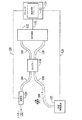
図1は、入力信号を減衰させてヘテロダインビート信号の信号対雑音比を改善し、受信器を飽和及び損傷から保護することができるヘテロダインベースの光スペクトル分析器(OSA)の一実施形態を示す。ヘテロダインベースのOSAは、信号ファイバ104、減衰器124、局部発振器源105、局部発振器ファイバ108、光カプラ110、光受信器112、プロセッサ116、及びフィードバック接続126を含む。説明全体を通じて、類似の構成要素を特定するために同じ参照番号を用いることがあることに留意されたい。
FIG. 1 illustrates one embodiment of a heterodyne-based optical spectrum analyzer (OSA) that can attenuate the input signal to improve the signal-to-noise ratio of the heterodyne beat signal and protect the receiver from saturation and damage. . The heterodyne-based OSA includes a
信号ファイバ104は、システムによって検出されるべき入力信号102を伝送する。一実施形態では、信号ファイバは、当該技術分野において知られているような単一モード光ファイバである。説明全体を通じて、光ファイバ内を伝送される光信号は、代案として他の導波路又は自由空間内で伝送され得る。
The
入力信号102は、光通信システムの分野において知られているような、従来の装置から生成される高コヒ―レント光信号を含む。例えば、入力信号は、単一レーザ又は複数のレーザから生成されることができ、波長分割多重の分野において知られているような単一波長又は複数の波長からなることができる。入力信号は、しばしばディジタル情報を搬送するために変調される。代わりに、入力信号はアナログ情報を搬送するために変調され得る。説明全体を通じて、光信号は、可視スペクトル、赤外スペクトル、又は任意の他の光スペクトル内の信号を含むことができる。
The
一実施形態では、入力信号102は、光スペクトル分析器により測定される未知の光学特性を有する。代案として、入力信号は、既知の光学特性でもって入力される光信号であってもよく、その場合、光スペクトル分析器は光ネットワーク分析に利用され得る。光スペクトル分析器を光ネットワーク又は構成要素の分析に利用する場合、ネットワーク又は単一の構成要素の特性は、ネットワーク又は単一の構成要素に既知の入力信号を入力し、そしてこの既知の信号に対する応答を測定することにより求められ得る。
In one embodiment, the
減衰器124は、入力信号を減衰させる光装置である。一実施形態では、減衰器は入力信号102を減衰させるために入力ファイバ104と一体化される。特定の種類の減衰器が不可欠ではなく、したがって光減衰の分野で知られているような様々なタイプの減衰器を用いることができる。減衰器の例には、ビームブロッキング減衰器、回析光学減衰器、、及び可変中性フィルタ減衰器が含まれる。好ましくは、減衰器は光カプラ110へ送られる入力信号電力の制御の必要に応じて減衰レベルを変えることができるように調整可能である。一実施形態では、減衰器は入力信号の伝送を完全に阻止するように調整され得る。以下に説明されるように、入力信号の完全な伝送遮断は、最適減衰レベル及び最小減衰レベルの確立に有用となり得る。
The
一実施形態では、減衰器の全スペクトルにわたって入力信号に減衰を適用する。すなわち、減衰スペクトルは入力信号スペクトルに比べて広い。さらに、一実施形態では、減衰レベルは波長に依存しない。すなわち、減衰レベルは関心のある波長範囲にわたって比較的一定である。 In one embodiment, attenuation is applied to the input signal over the entire spectrum of the attenuator. That is, the attenuation spectrum is wider than the input signal spectrum. Further, in one embodiment, the attenuation level is independent of wavelength. That is, the attenuation level is relatively constant over the wavelength range of interest.
局部発振器源105は、局部発振器信号106を生成する。一実施形態では、局部発振器源は、1ナノメートル又はそれより大きい波長範囲にわたって連続的に調整できる高コヒーレント同調可能レーザである。光スペクトル分析中、局部発振器源は、或る範囲の周波数又は波長にわたって入力信号を検出するために、この範囲の周波数又は波長にわたって掃引される高コヒ―レント局部発振器信号を生成する。一実施形態では、1,550nmの局部発振器信号の掃引速度は、約40nm/s又は6.15MHz/μsであり、掃引範囲は約100nmであるが、掃引速度や掃引範囲は、より高く、又はより低くすることができる。
The
局部発振器ファイバ108は、局部発振器信号106を光カプラ110へ伝送する単一モード光ファイバなどの光ファイバである。
The
光カプラ110は、入力信号102と掃引される局部発振器信号106を共通の導波路上へ合成する。図1に示されるように、光カプラは入力信号と掃引される局部発振器信号を合成し、合成された光信号(以降、合成光信号と称する)を出力ファイバ118、120へ分配する。光カプラ110は、光学的方向性の3dBファイバカプラとすることができるが、他の光カプラを用いてもよい。一実施形態では、光カプラは、入力信号102と掃引される局部発振器信号106の波長と偏光に実質的に無関係である。一実施形態では、光カプラは単一モードカプラである。図1の実施形態では、減衰器124は、信号ファイバ104を介して光カプラに光学的に結合される。
The
出力ファイバ118、120は、光カプラ110からヘテロダイン受信器112へ合成光信号の二つの部分を伝送する単一モード光ファイバである。
The
光受信器112は、光カプラ110から合成光信号を受信するように結合される。光受信器は、受信光信号に応答して電気出力信号を生成する。一実施形態では、光受信器は二乗検波を利用し、それにより入力信号102と掃引される局部発振器信号106の混合という結果となる。二つの光信号の混合により、入力信号と掃引される局部発振器信号との間の周波数差分に等しい周波数でヘテロダインビート信号が生成される。高コヒ―レント入力信号及び局部発振器信号に関して、結果として生じたヘテロダインビート信号は、ヘテロダインビート信号の線形変化周波数から生じる二次関数の位相挙動を有する。一実施形態では、ヘテロダインビート信号は電気接続152を介して信号プロセッサ116へ供給される。ヘテロダインビート信号に加えて、出力信号(すなわち入力信号及び局部発振器信号からの雑音成分)の他の部分は、受信器で識別され、プロセッサに供給される。
The
図1のシステムは、光受信器へ合成光信号の二つの部分を供給することを含むが、他の実施形態は、受信器へ合成光信号の単一部分を供給することを含むこともできる。合成光信号の単一例の場合、光カプラは一つの出力だけを必要とし、光受信器には一つの光検出器だけが必要である。図1の別の代替実施形態は、光受信器へ合成光信号の三つ以上の部分を供給することを含む。一実施形態では、合成光信号の四つの独立した部分が光受信器へ供給される。 Although the system of FIG. 1 includes providing two portions of the combined optical signal to the optical receiver, other embodiments may include providing a single portion of the combined optical signal to the receiver. In the case of a single example of a combined optical signal, the optical coupler only needs one output and the optical receiver only needs one photodetector. Another alternative embodiment of FIG. 1 involves providing three or more portions of the combined optical signal to an optical receiver. In one embodiment, four independent portions of the combined optical signal are provided to an optical receiver.
プロセッサ116は、光受信器112から出力信号を受信し、入力信号102の光周波数、波長、または振幅といった光学パラメータを示す出力を生成する。プロセッサは、信号処理の分野で知られているように、アナログ信号処理回路、ディジタル信号処理回路、又はソフトウェア、或いはそれらの任意の組み合わせを含むことができる。図1の実施形態では、プロセッサは光受信器からディジタルヘテロダインビート信号データを受信し、プロセッサがディジタル処理を実行する。代替の実施形態では、プロセッサは光受信器からアナログヘテロダインビート信号を受信し、アナログ信号はプロセッサによりディジタルデータへ変換される。ディジタルデータは引き続いて処理され、入力信号の光学パラメータを示す出力を生成する。
The
入力信号の光学パラメータを示す出力を生成することに加えて、プロセッサは、最適減衰レベル及び最小減衰レベルを求めること、及び入力信号に適用される減衰量を制御することなどの他の機能も実行することができる。最適減衰レベル及び最小減衰レベルを求める機能を、以下に詳細に説明する。図1の実施形態では、プロセッサは、以下に説明される機能を実行するための減衰制御モジュール122を含む。一実施形態では、減衰制御モジュールは、以下に説明された機能を実行するための特定機能ソフトウェアを含む。一実施形態では、プロセッサと減衰制御モジュールは、光ヘテロダイン検出システムの動作を制御するために利用されるコンピュータ制御システムに具現化される。
In addition to generating an output indicative of the optical parameters of the input signal, the processor also performs other functions such as determining an optimal attenuation level and a minimum attenuation level, and controlling the amount of attenuation applied to the input signal. can do. The function for determining the optimum attenuation level and the minimum attenuation level will be described in detail below. In the embodiment of FIG. 1, the processor includes a damping
一実施形態では、プロセッサ116と減衰器124との間に接続126が設けられ、プロセッサと局部発振器源105との間に接続128が設けられる。これらの接続により、プロセッサは減衰器と局部発振器源を制御することが可能になる。
In one embodiment, a
図1の実施形態において、光受信器112は、光ヘテロダイン検出システムの分野で知られているような、光検出器、増幅器、抵抗器、及びフィルタを含む。図2は、平衡検出を達成するために光ヘテロダイン検出システムで利用され得る光受信器例の拡大図を示す。光受信器は、光検出器、トランスインピーダンス増幅器、帯域フィルタ、減算器、及びスクエアリングユニットを含む。トランスインピーダンス増幅器は、光電流Δi1とΔi2を電圧へ変換する。光電流Δi1とΔi2の大きさは、光パワーP1、P2と光検出器の応答性に比例する。トランスインピーダンス増幅器から生成された電圧は、幅Bを備えた周波数fBの狭帯域フィルタを通過させられる。フィルタからの出力は、利得G=R2/R1を有する第2段の増幅器により増幅される。減算器は、電圧ΔV1、ΔV2を減算し、スクエアリングユニットが減算器から出力された信号を二乗演算する。
In the embodiment of FIG. 1,
図2に示したシステム及び光受信器の場合、入力信号PSは、カプラ210内で局部発振器信号PLと合成される前に係数「α」で減衰される。本例では、カプラは通過効率a2と横断(across)効率1−a2を有するものと仮定しており、ここでは理想的な50:50のカプラの場合、a2=1/2である。光検出器205、209での光信号は、以下の式
P1=a2PL+(1−a2)αPS
+2a√(1−a2)√(PLαPS)cos(Δω・t+Δθ) (3)
P2=(1−a2)PL+a2αPS
−2a√(1−a2)√(PLαPS)cos(Δω・t+Δθ) (4)
の形態を有しており、ここでΔω(とΔθ)は、ヘテロダインビート信号の差分周波数(と差分位相)である。完全なカプラ(a2=1/2)の場合、P1とP2の減算がヘテロダインビート項以外の全てを消去する。一般に、完全な結合を達成することは現実的ではない。さらに、二つの光検出器の応答における変化によって、ヘテロダインビート項をきれいに抽出するのに補償されなければならない差分がさらに導入される。
For the system and optical receiver shown in FIG. 2, the input signal P S is attenuated by a factor “α” before being combined with the local oscillator signal P L in
+ 2a√ (1-a 2) √ (P L αP S) cos (Δω · t + Δθ) (3)
P 2 = (1−a 2 ) P L + a 2 αP S
-2a√ (1-a 2) √ (P L αP S) cos (Δω · t + Δθ) (4)
Where Δω (and Δθ) is the difference frequency (and difference phase) of the heterodyne beat signal. For a perfect coupler (a 2 = 1 /), the subtraction of P 1 and P 2 eliminates everything but the heterodyne beat term. In general, achieving a perfect connection is not practical. Furthermore, changes in the response of the two photodetectors introduce further differences that must be compensated for to cleanly extract the heterodyne beat term.
光ヘテロダイン検出システムによって最終的に測定される信号は、個々の検出回路からの二つの出力電圧(ΔV1とΔV2)を含む。上述のように、検出回路は光電流Δi1とΔi2を電圧に変換するトランスインピーダンス増幅器から構成される。これらの電圧は、利得G=R2/R1を有する第2段の増幅器により増幅される前に幅Bを備える周波数fBの狭帯域通過フィルタを通過させられる。光電流Δi1とΔi2は、一実施形態では1mA/mWのオーダであるフォトダイオードの応答性を通じて光パワーP1とP2に関係する。最終的な所望の出力信号は、下記の式により与えられる:
S=(ΔV1−ΔV2)2=ΔV1 2+ΔV2 2−2ΔV1ΔV2 ,(5)
The signal ultimately measured by the optical heterodyne detection system includes the two output voltages (ΔV 1 and ΔV 2 ) from the individual detection circuits. As described above, the detection circuit includes a transimpedance amplifier that converts the photocurrents Δi 1 and Δi 2 into voltages. These voltages are passed through a narrow band pass filter of frequency f B with a width B before being amplified by the amplifier of the second stage having a gain G = R 2 / R 1. The photocurrents Δi 1 and Δi 2 are related to the optical powers P 1 and P 2 through the response of the photodiode, which in one embodiment is on the order of 1 mA / mW. The final desired output signal is given by:
S = (ΔV 1 -ΔV 2) 2 =
測定された信号は二つの成分からなり、すなわちΔV1 2とΔV2 2によって与えられる個々の検出器の分散、並びにΔV1ΔV2によって与えられる検出器間の共分散である。光学的なショット雑音と熱雑音は、光検出器にわたって相関されていないとみなされ、それ故に検出器の分散に寄与するだけである。強度雑音(RIN)並びにヘテロダインビート信号は、光検出器間に明確な位相関係(ただし、逆符号)を有しており、それ故に二つの光検出器の分散と共分散の両方に寄与する。受信器端に見られる周波数成分だけが帯域通過フィルタによって許容される周波数成分であると仮定している。RIN、ショット雑音、及び熱雑音は、幅Bを備える周波数fBで計算されなければならない。観測されるビート信号は、PS(νS)のその部分に対応し、ここで局部発振器信号PL(νL)は周波数において|fB|だけ離れている(そのためΔν=νL−νS=±fB)。局部発振器信号を或る周波数範囲にわたって掃引すると、これによって望み通りにPS(νS)が写像される。 The measured signal consists of two components, namely the dispersion of [Delta] V 1 2 and [Delta] V 2 of the individual provided by second detector, and the covariance between the detector given by [Delta] V 1 [Delta] V 2. Optical shot noise and thermal noise are considered uncorrelated across the photodetector and therefore only contribute to the dispersion of the detector. The intensity noise (RIN) as well as the heterodyne beat signal have a well-defined phase relationship between the photodetectors (but with the opposite sign) and therefore contribute to both the variance and covariance of the two photodetectors. It is assumed that only the frequency components seen at the receiver end are the frequency components allowed by the bandpass filter. RIN, shot noise, and thermal noise must be calculated at frequency f B with width B. Beat signal observed corresponds to the portion of P S (ν S), wherein the local oscillator signal P L (ν L) in the frequency | f B | just apart (so Δν = ν L -ν S = ± f B ). When the local oscillator signal is swept over a frequency range, this maps P S (ν S ) as desired.
出力信号の分散と共分散は以下に与えられる。 分散 The variance and covariance of the output signal are given below.

ここで「a」はカプラ効率のパラメータであり、二つの光検出器の応答はRe1、Re2により与えられ、各回路の熱雑音はJ1、J2により与えられ、GとRfにより与えられる様々な回路利得は先に定義されており、RIN/ショット雑音項は明示されている。これらの「雑音」項は、通過帯域周波数fBで算出されなければならない。ビート項PLPSは、周波数においてfBだけ離れたスペクトル成分PL(νL)及びPS(νS)に関係する。a2≒1/2と仮定することにより、信号Sは以下のように計算され得る。 Where “a” is a parameter of the coupler efficiency, the response of the two photodetectors is given by Re 1 , Re 2 , the thermal noise of each circuit is given by J 1 , J 2 , and G and R f The various circuit gains given are defined above and the RIN / shot noise terms are specified. These "noise" term, must be calculated in the pass band frequency f B. Beat claim P L P S is related to the spectral components separated by f B in the frequency P L (ν L) and P S (ν S). Assuming that a 2 ≒ 1/2, the signal S can be calculated as follows:
ここで、平均検出器応答と利得(Re,G,Rf)は、RIN雑音に関する減算パラメータΔLとΔSに包含される変化量を備えるものと仮定されている。 Here, the average detector response and gain (Re, G, R f) is assumed to comprise a variation to be included in the subtraction parameter delta L and delta S about RIN noise.
制御された減衰を備えるヘテロダインベースのOSAの動作を、図1〜図9に関連して説明する。動作中、入力信号102は減衰器124を通って伝送され、入力信号は所望レベルに減衰される。減衰された入力信号は、次に光カプラ110の方へ入力ファイバ104を介して案内される。同時に、局部発振器源105は、掃引される局部発振器信号106を生成し、その信号106は局部発振器ファイバ108を介して光カプラに伝送される。減衰された入力信号102と掃引される局部発振器信号106は、光カプラにより合成光信号へ合成される。合成光信号は、出力ファイバ118と120上へ出力され、ヘテロダイン受信器112へ伝送される。合成光信号は、ヘテロダイン受信器により検出されて混合され、合成光信号に応答してヘテロダインビート信号が生成される。ヘテロダインビート信号は、プロセッサ116へ出力される。プロセッサは、ヘテロダインビート信号を用いて、波長、周波数、又は振幅といった入力信号の光学パラメータを示す出力を生成する。
The operation of a heterodyne-based OSA with controlled attenuation will be described with reference to FIGS. In operation,
上述のように、入力信号を減衰させて信号対雑音比を改善することは、入力信号の強度雑音が主雑音源であるときに実行されるのが好ましい。この条件下では、入力信号の減衰がヘテロダインビート信号の信号対雑音比を改善する。その理由は、入力信号の強度雑音とヘテロダインビート信号が入力信号の減衰とともに別々に変培されるからである。好ましくは、入力信号はヘテロダインビート信号の信号対雑音比を最大にするレベルまで減衰される。一実施形態では、入力信号は最適減衰レベルまで減衰され、この場合、最適減衰レベルは入力信号の減衰を通じて達成可能な最大の信号対雑音比か、又はほぼ最大の信号対雑音比を生成する減衰レベルとして定義される。例えば、最適減衰レベルは入力信号の減衰を通じて達成可能な最大の信号対雑音比の数dB以内にある信号対雑音比を達成することができる。一実施形態では、入力信号の強度雑音が二番目に大きな雑音源にほぼ等しくなるように入力信号を減衰した際に、信号対雑音比が最大化される。例えば、二番目に大きな雑音源は、局部発振器信号のショット雑音か、入力信号のショット雑音か、局部発振器信号の強度雑音か、光受信器からの電気的雑音か、又はそれらの幾つかの組み合わせとすることができる。 As described above, attenuating the input signal to improve the signal-to-noise ratio is preferably performed when the intensity noise of the input signal is the main noise source. Under these conditions, the attenuation of the input signal improves the signal-to-noise ratio of the heterodyne beat signal. The reason is that the intensity noise of the input signal and the heterodyne beat signal are separately multiplied together with the attenuation of the input signal. Preferably, the input signal is attenuated to a level that maximizes the signal-to-noise ratio of the heterodyne beat signal. In one embodiment, the input signal is attenuated to an optimal attenuation level, where the optimal attenuation level is the attenuation that produces the maximum or nearly maximum signal-to-noise ratio achievable through attenuation of the input signal. Defined as a level. For example, the optimal attenuation level can achieve a signal to noise ratio that is within a few dB of the maximum signal to noise ratio achievable through attenuation of the input signal. In one embodiment, the signal-to-noise ratio is maximized when the input signal is attenuated such that the intensity noise of the input signal is approximately equal to the second largest noise source. For example, the second largest noise source may be shot noise of the local oscillator signal, shot noise of the input signal, intensity noise of the local oscillator signal, electrical noise from the optical receiver, or some combination thereof. It can be.
特定の入力信号に関する最適減衰レベルは、異なる減衰レベルの範囲にわたる減衰の関数としてヘテロダインビート信号と雑音を直接的に測定し、それぞれの異なる減衰レベルでの対応する信号対雑音比を計算し、次いで最大の信号対雑音比に対応する減衰レベルを特定することにより求められ得る。これが最適減衰レベルを求めるための信頼できる技術ではあるが、この技術は、異なる減衰レベルにおいてヘテロダインビート信号を複数回測定して、信号対雑音比を計算できるようにすることが必要である。異なる減衰レベルにおいてヘテロダインビート信号を複数回測定することは、時間を浪費し、不要な誤差を導入する可能性がある。 The optimal attenuation level for a particular input signal is to directly measure the heterodyne beat signal and noise as a function of attenuation over a range of different attenuation levels, calculate the corresponding signal-to-noise ratio at each different attenuation level, and then It can be determined by specifying the attenuation level corresponding to the maximum signal-to-noise ratio. While this is a reliable technique for determining the optimal attenuation level, it requires that the heterodyne beat signal be measured multiple times at different attenuation levels so that the signal-to-noise ratio can be calculated. Measuring the heterodyne beat signal multiple times at different attenuation levels can be time consuming and introduce unnecessary errors.
本発明による一実施形態では、入力信号に関する最適減衰レベルは、ヘテロダインビート信号の測定値を得ることなく求められる。具体的には、最適減衰レベルは様々な雑音測定値から算出される。一実施形態では、入力信号に関する最適減衰レベルは、減衰の関数として様々な雑音測定値を取得し、得られた雑音測定値を信号対減衰曲線に当てはめ、次いで適合する曲線からのデータを用いて最適な減衰レベルを計算することにより求められる。 In one embodiment according to the present invention, the optimal attenuation level for the input signal is determined without taking measurements of the heterodyne beat signal. Specifically, the optimal attenuation level is calculated from various noise measurements. In one embodiment, the optimal attenuation level for the input signal is obtained by taking various noise measurements as a function of attenuation, fitting the obtained noise measurements to a signal versus attenuation curve, and then using data from the fitted curve. It is determined by calculating the optimal attenuation level.
光ヘテロダイン検出システムに関して、減衰α(ここで、最大減衰時α=0であり、最小減衰時α=1である)の関数としての出力信号Sは、
S(α)=Aα2+(B+D)α+C (15)
により表わされることができ、ここで様々な定数は以下のようになる。
A=ΔS・RINS・B・<PS>2 (16)
B=q・B・<PS> (17)
C=q・B・<PL>+ΔL・RINL・B・<PL>2
+(J1 2+J2 2)/Re2G2Rf 2 (18)
D=4・<PL>・<PS>・B/ΔνS (19)
For an optical heterodyne detection system, the output signal S as a function of the attenuation α (where α = 0 at maximum attenuation and α = 1 at minimum attenuation) is:
S (α) = Aα 2 + (B + D) α + C (15)
Where the various constants are as follows:
A = Δ S · RIN S · B · <P S> 2 (16)
B = q · B · <P S> (17)
C = q · B · <P L > + Δ L · RIN L · B · <P L > 2
+ (J 1 2 + J 2 2) / Re 2 G 2 R f 2 (18)
D = 4 · <P L > · <P S > · B / Δν S (19)
上記式では、A項が入力信号の強度雑音を表わし、B項が入力信号のショット雑音を表わし、C項が局部発振器信号と光受信器からの雑音の組み合わせを表わす。D項は、信号Sのヘテロダインビート部分(本明細書において、ヘテロダインビート信号またはShbと呼ぶ)を表わす。 In the above equation, the A term represents the intensity noise of the input signal, the B term represents the shot noise of the input signal, and the C term represents the combination of the local oscillator signal and the noise from the optical receiver. The D term represents the heterodyne beat portion of signal S (referred to herein as the heterodyne beat signal or Shb ).
上記式が与えられると、減衰の関数としてのヘテロダインビート信号対雑音比(本明細書において、信号対雑音比と呼ぶ)は、以下のように表され得る:
Shb(α)/N(α)=Dα/(Aα2+Bα+C) (20)
Given the above equation, the heterodyne beat signal to noise ratio (referred to herein as the signal to noise ratio) as a function of attenuation may be expressed as:
Shb (α) / N (α) = Dα / (Aα 2 + Bα + C) (20)
信号対雑音の式が与えられると、信号対雑音比を最大化するαの最適値は、信号対雑音の式の導関数を取り、導関数をゼロに等しく設定し、αについて解くことにより求められ得る。この計算の実行により、所定の定数
αopt=√(C/A) (21)
の項で最適減衰レベルの式が与えられる。
Given the signal-to-noise equation, the optimal value of α that maximizes the signal-to-noise ratio is determined by taking the derivative of the signal-to-noise equation, setting the derivative equal to zero, and solving for α. Can be By performing this calculation, a predetermined constant α opt = √ (C / A) (21)
Gives the equation for the optimal attenuation level.
最適減衰レベルαoptを計算するために、定数項AとCの値を求めなければならない。前述のように、C項は局部発振器信号と受信器からの雑音の組み合わせを表わし、αの関数ではない。C項は、入力信号の無い状態で局部発振器信号に応答して生成される出力信号を測定することにより求められ得る。局部発振器信号に応答し、入力信号の無い状態での出力信号の測定値は、本明細書において「基礎測定値」と呼ぶ。一実施形態では、C項は、入力信号をシステムに送り込む前に局部発振器信号の存在下で求められる。別の実施形態では、C項は、入力信号が完全に減衰された状態で、局部発振器信号の存在下で求められる。 To calculate the optimal attenuation level α opt , the values of the constant terms A and C must be determined. As mentioned above, the C term represents the combination of the local oscillator signal and the noise from the receiver and is not a function of α. The C term can be determined by measuring an output signal generated in response to a local oscillator signal in the absence of an input signal. The measured value of the output signal in the absence of the input signal in response to the local oscillator signal is referred to herein as the "basic measured value." In one embodiment, the C term is determined in the presence of a local oscillator signal before feeding the input signal into the system. In another embodiment, the C term is determined in the presence of a local oscillator signal with the input signal fully attenuated.
上述のように、A項は入力信号の強度雑音を表わす。A項が減衰(すなわちα)と共に二次関数的に変化する唯一の項であるため、A項はαに関する出力信号Sの二次導関数をとることにより求められ得る。これは、局部発振器信号の有無に拘わらず行なうことができる。得られる関係は、
A=(1/2)δ2S/δα2 (22)
ただし、
S=(ΔV1−ΔV2)2 (23)
As mentioned above, the A term represents the intensity noise of the input signal. Since the A term is the only term that varies quadratically with attenuation (ie, α), the A term can be determined by taking the second derivative of the output signal S with respect to α. This can be done with or without a local oscillator signal. The resulting relationship is
A = (1/2) δ 2 S / δα 2 (22)
However,
S = (ΔV 1 −ΔV 2 ) 2 (23)
二次導関数を測定するために、出力信号Sのサンプル測定値を異なる減衰レベルで採取する。次いで、出力信号のサンプル測定値は、出力信号対減衰(すなわちS対α)曲線に当てはめられる。一実施形態では、出力信号のサンプル測定値をS対α曲線の二次多項式に代入する。一実施形態では、出力信号の測定値は最小二乗法の最小化などの非線形当てはめルーチンを用いて二次多項式に代入される。一実施形態では、サンプル測定値は、局部発振器信号の無い状態で採取される(局部発振器信号が存在しないので、ヘテロダインビート信号は一切生成されない)。サンプル測定値は、局部発振器信号と存在する入力信号の両方と共に採取され得る(混合の結果としてヘテロダインビート信号が存在するが、ヘテロダインビート信号は雑音信号から抽出されない)。 Take sample measurements of the output signal S at different attenuation levels to measure the second derivative. The sample measurements of the output signal are then fitted to an output signal versus decay (ie, S versus α) curve. In one embodiment, the sample measurements of the output signal are substituted into a second order polynomial of the S versus α curve. In one embodiment, the measurement of the output signal is substituted into a second-order polynomial using a non-linear fitting routine, such as least-squares minimization. In one embodiment, the sample measurements are taken in the absence of a local oscillator signal (no heterodyne beat signal is generated because no local oscillator signal is present). Sample measurements may be taken with both the local oscillator signal and the input signal present (a heterodyne beat signal is present as a result of the mixing, but the heterodyne beat signal is not extracted from the noise signal).
入力信号の強度雑音が測定不能である場合、A項をゼロに設定し、それにより入力信号の減衰を通じて信号対雑音比の増加が一切達成されないことを示さねばならない。サンプル測定値から得られるA項が非常に小さい場合、αoptの値は最大値「1」、すなわち光検出器を非飽和状態に保つ値に限定されるべきである。 If the intensity noise of the input signal is not measurable, the A term must be set to zero, thereby indicating that no increase in signal-to-noise ratio is achieved through attenuation of the input signal. If the A term from the sample measurements is very small, the value of α opt should be limited to a maximum value “1”, ie, a value that keeps the photodetector unsaturated.
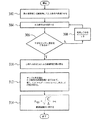
図3は、光ヘテロダイン検出システムの入力信号に関する最適減衰レベルを求めるためのプロセス流れ図の一実施形態を示す。ブロック302では、入力信号は、減衰無しか、又は最小許容減衰でもって減衰器を通過させられる(最小許容減衰を求めることは後述する)。ブロック304では、減衰された入力信号に応答して出力信号Sを測定する。判断ブロック306では、出力信号の十分なサンプル測定値が得られたか否かを判断する。十分なサンプル測定値が存在しないと判断された場合、ブロック308において減衰レベルをインクリメントする。すなわち、入力信号に適用される減衰レベルは、いくらかの増分量だけ増加する。αの観点から減衰に注目すると、減衰レベルをインクリメントすることはαをデクリメントすることを意味する。一実施形態では、減衰レベルは2〜7dBの間隔でインクリメントされるが、他の間隔を用いてもよい。減衰レベルをインクリメントした後に、ブロック304において出力信号を再測定する。
FIG. 3 illustrates one embodiment of a process flow diagram for determining an optimal attenuation level for an input signal of an optical heterodyne detection system. In
判断ブロック306に戻って、十分なサンプル測定値が存在すると判断された場合、ブロック310において出力信号の基礎測定値が得られる。一実施形態では、出力信号の基礎測定値は、αoptの式中のC項を求めるために使用される。C項は局部発振器信号と受信器からの雑音の組み合わせを表わすため、基礎測定値は、局部発振器信号が存在し、かつ入力信号の無い状態で得られる。基礎測定値を得た後、ブロック312において、出力信号のサンプル測定値を出力信号対減衰曲線に当てはめる。一実施形態では、サンプル測定値は、減衰の関数としての出力信号の二次多項式S(α)=Aα2+(B+D)α+Cに代入される。A項とC項を求めた後、ブロック314において最適減衰は以下の式から計算される:
αopt=√(C/A) (21)
Returning to decision block 306, if it is determined that there are sufficient sample measurements, a basic measurement of the output signal is obtained at
α opt = √ (C / A) (21)
図3のプロセス流れ図は、プロセスステップの特定順序を示す。プロセスステップは、本発明の範囲から逸脱することなく図3に示された順序から変更され得る。例えば、減衰レベルのインクリメント(ブロック308)を出力信号の測定(ブロック304)後に行なっているが、代替の実施形態では、プロセスステップは、十分なサンプル測定値が存在するか否かの判断(判定点306)の前に行われるように順序付けられ得る。さらに、代替の実施形態では、サンプル測定値を得る(ブロック304)前か、又はサンプル測定値を出力信号対減衰曲線に当てはめた(ブロック312)後に、基礎測定値を得ることができる(ブロック310)。別の代案では、サンプル測定値は、初期減衰レベルを高く設定し、減衰レベルをデクリメントして必要とされるサンプル測定値を得ることにより取得され得る。別の代案において、サンプル測定値は減衰レベルをランダムに変えることにより取得され得る。 プ ロ セ ス The process flow diagram of FIG. 3 illustrates the specific order of the process steps. The process steps may be changed from the order shown in FIG. 3 without departing from the scope of the present invention. For example, although the attenuation level is incremented (block 308) after the measurement of the output signal (block 304), in an alternative embodiment, the process step determines whether there are sufficient sample measurements (decision). It can be ordered to occur before point 306). Further, in an alternative embodiment, a base measurement may be obtained (block 310) either before obtaining the sample measurement (block 304) or after fitting the sample measurement to the output signal versus attenuation curve (block 312). ). In another alternative, the sample measurement may be obtained by setting the initial attenuation level high and decrementing the attenuation level to obtain the required sample measurement. In another alternative, a sample measurement may be obtained by randomly varying the attenuation level.
出力信号対減衰応答を特徴付けるのに十分なサンプルの数は、実施に固有である。一実施形態では、出力信号対減衰曲線に当てはめるために、少なくとも三つのサンプル測定値が得られる。 The number of samples sufficient to characterize the output signal versus the damped response is implementation specific. In one embodiment, at least three sample measurements are obtained to fit the output signal versus attenuation curve.
図4は、光ヘテロダイン検出システムの入力信号に関して最適減衰レベルを求めるためのプロセス流れ図の別の実施形態を示す。ブロック402では、出力信号の基礎測定値は、局部発振器信号に応答し、かつ入力信号の無い状態で得られる。ブロック404では、出力信号のサンプル測定値は、異なる減衰レベルの関数として入力信号に応答して得られる。ブロック406では、最適減衰レベルは、基礎測定値及びサンプル測定値の関数として求められる。
FIG. 4 illustrates another embodiment of a process flow diagram for determining an optimal attenuation level for an input signal of an optical heterodyne detection system. At
ヘテロダインビート信号の信号対雑音比を改善するように減衰を制御することに加えて、減衰は、光検出器が飽和したり、又は永久的に損傷したりすることから保護するために制御され得る。一実施形態では、各光検出器に関連する直流(DC)電圧は、光検出器の保護のために中間の検出点から監視される。例えば、図2を参照すると、受信光信号に応答して生成されるDC電圧は、個々の帯域フィルタより前にある検出点230と232から監視される。すなわち、トランスインピーダンス増幅器のDC電圧出力が帯域フィルタリング前に測定されるように検出点を配置する。
In addition to controlling the attenuation to improve the signal-to-noise ratio of the heterodyne beat signal, the attenuation can be controlled to protect the photodetector from saturation or permanent damage . In one embodiment, the direct current (DC) voltage associated with each photodetector is monitored from an intermediate detection point for photodetector protection. For example, with reference to FIG. 2, the DC voltage generated in response to the received optical signal is monitored from
光ヘテロダイン検出システムの光検出器を保護するために入力信号の減衰を制御するためのプロセス例を、三つの異なる状況「コールドスタート」、「通常動作」、「電源遮断」に関して説明する。コールドスタートでは、光検出器は、入力信号からの光パワーサージから保護されなければならない。光検出器を光パワーサージから保護することは、最初に電源投入時に減衰を最大減衰レベルに設定し、次いで光検出器が特定のDC電圧限界に達するまで入力信号の減衰を徐々に低減することにより達成される。光検出器がそれらのDC電圧限界に達する点は、許容さるべき最小減衰レベルとして設定される。すなわち、電源投入時にパワーサージにより飽和したり、又は損傷したりすることから光検出器を保護するために、入力信号の減衰は、設定された最小減衰レベル未満に低下させてはならない。最大減衰でα=0、最小減衰でα=1として減衰をαの観点から説明したので、最小減衰レベルはαの最大値すなわちαmaxによって表わされる。すなわち、αmaxは、光検出器を損傷から保護するために入力信号に適用されるべき最小減衰レベルである。 An example process for controlling the attenuation of an input signal to protect a photodetector of an optical heterodyne detection system is described for three different situations: "cold start", "normal operation", and "power down". In a cold start, the photodetector must be protected from optical power surges from the input signal. Protecting the photodetector from optical power surges involves first setting the attenuation to the maximum attenuation level at power up, and then gradually reducing the attenuation of the input signal until the photodetector reaches a specific DC voltage limit. Is achieved by The point at which the photodetectors reach their DC voltage limit is set as the minimum attenuation level to be allowed. That is, the input signal attenuation must not be reduced below the set minimum attenuation level to protect the photodetector from being saturated or damaged by power surges at power up. Since the attenuation has been described in terms of α with α = 0 at the maximum attenuation and α = 1 at the minimum attenuation, the minimum attenuation level is represented by the maximum value of α, that is, α max . That is, α max is the minimum attenuation level that should be applied to the input signal to protect the photodetector from damage.
本明細書において定義されたように、光検出器のDC電圧限界(電圧限界とも呼ぶ)は、それを超えると光検出器が線形応答をもたらすと見なせなくなる測定電圧である。すなわち、光検出器は、電圧限界を含む測定電圧に対して線形応答を有すると仮定されている。電圧限界を超える測定電圧については、線形応答と見なすことはできない。一実施形態では、電圧限界は光検出器特性の関数として予め確立された値である。 DCAs defined herein, the DC voltage limit of a photodetector (also called the voltage limit) is the measured voltage beyond which the photodetector cannot be considered to provide a linear response. That is, the photodetector is assumed to have a linear response to the measured voltage, including the voltage limit. A measured voltage that exceeds the voltage limit cannot be considered a linear response. In one embodiment, the voltage limit is a pre-established value as a function of the photodetector characteristics.
図5は、光ヘテロダイン検出システムのコールドスタート時の最小減衰レベルを求めるための技術のプロセス流れ図を示す。ブロック502では、減衰レベルが最大レベル(すなわちα=0)に設定される。ブロック504では、DC検出器が電源投入される。ブロック506では、減衰レベルを電流減衰レベルからデクリメントする。すなわち、減衰レベルは増分量だけ減少される。αの観点から減衰に注目すると、減衰レベルのデクリメントはαをインクリメントすることを意味する。ブロック508では、減衰が最低の可能な減衰レベル(すなわち、一切減衰がなくα=1)にあるかどうかが判定される。減衰が最低の可能な減衰レベルにある場合、ブロック514において、最小減衰レベルは最低の可能な減衰レベル(すなわち、αmax=1)として設定される。減衰レベルが最低減衰レベルにない場合、ブロック510において、各光検出器に関連したDC電圧を測定する。ブロック512では、各光検出器の測定されたDC電圧が個々の光検出器のDC電圧限界に達したかどうかについて判定がなされる。DC電圧がDC電圧限界に達しなかった場合、プロセスはブロック506へ戻り、そこで減衰レベルが再度デクリメントされる。DC電圧がDC電圧限界に達した場合、ブロック514において電流減衰レベルを最小減衰レベルとして設定する。αの観点から減衰に注目すると、電流減衰レベルはαmaxとして保存される。最小減衰レベルを設定した後、光ヘテロダイン検出システムの他の構成要素(すなわち局部発振器源、変調器)は、ブロック516で電源投入され、システムはブロック518で通常動作に入る準備が整う。
FIG. 5 shows a process flow diagram of a technique for determining a minimum cold start attenuation level of an optical heterodyne detection system. At
通常動作中、光検出器は入力信号からの光パワーサージから保護されなければならない。光検出器を光パワーサージから保護することは、光検出器に関連するDC電圧をアクティブに監視し、光検出器が飽和した場合に減衰を最大減衰レベルに設定し、次いで光検出器が事前に設定されたDC電圧限界に達するまで入力信号の減衰を徐々に低減することにより達成される。光検出器がそれらのDC電圧限界に達する点は、通常動作中に許容されるべき最小の減衰レベルとして確立される。すなわち、光検出器が通常動作中に飽和又は損傷したりすることから保護し、光検出器がそれらの線形応答範囲内で動作するように保証するために、入力信号の減衰は、DC電圧限界に応答して確立された最小減衰レベル未満に低下させてはならない。前述のように、最大減衰でα=0、最小減衰でα=1と減衰をαの観点から説明したので、最小減衰レベルはαの最大値すなわちαmaxにより表わされる。すなわち、αmaxは光検出器を損傷から保護するために入力信号に適用されるべき最小減衰レベルである。 During normal operation, the photodetector must be protected from optical power surges from the input signal. Protecting the photodetector from optical power surges involves actively monitoring the DC voltage associated with the photodetector, setting the attenuation to the maximum attenuation level when the photodetector saturates, and then allowing the photodetector to This is achieved by gradually reducing the attenuation of the input signal until a DC voltage limit set at is reached. The point at which the photodetectors reach their DC voltage limit is established as the minimum attenuation level to be allowed during normal operation. That is, to protect the photodetectors from saturating or damaging during normal operation and to ensure that the photodetectors operate within their linear response range, the attenuation of the input signal is limited to the DC voltage limit. Must not be reduced below the minimum attenuation level established in response to As described above, the attenuation has been described from the viewpoint of α, that is, α = 0 for the maximum attenuation and α = 1 for the minimum attenuation. Therefore, the minimum attenuation level is represented by the maximum value of α, that is, α max . That is, α max is the minimum attenuation level that should be applied to the input signal to protect the photodetector from damage.
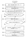
図6は、光ヘテロダイン検出システムの通常動作中に最小減衰レベルを求めるための技術のプロセス流れ図を示す。ブロック602では、光ヘテロダイン検出システムは通常動作モードにある。判断ブロック604では、光検出器が飽和しているか否かについて判定がなされる。一実施形態では、DC検出器が飽和しているか否かの判定には、DC電力レベルを検査すること、及び直流電力レベルが動作範囲にあるかどうか判定することが含まれる。一実施形態では、この判定は、DC検出点におけるDC電圧の定期的な測定に応答してなされる。例えば、DC検出点は、局部発振器信号の各掃引の後に監視され得る。光検出器が飽和していない場合、通常動作が続く(ブロック602)。光検出器が飽和している場合、ブロック606において減衰レベルを最大レベル(すなわち、α=0)に設定する。ブロック608では、減衰レベルを電流減衰レベルからデクリメントする。すなわち、減衰レベルは増分量だけ低減される。αの観点から減衰に注目すると、減衰レベルをデクリメントすることは、αをインクリメントすることを意味する。一実施形態では、減衰レベルは初回の反復の最初のレベルからデクリメントされ、そして次の反復の低減された減衰レベルからデクリメントされる。判断ブロック610では、減衰が最低の可能な減衰レベル(すなわち、減衰が無しでα=1)にあるかどうかが判断される。減衰が最低の可能な減衰レベルにある場合、ブロック616において、最小減衰レベルが最低の可能な減衰レベル(すなわち、αmax=1)として設定される。減衰レベルが最低の減衰レベルにない場合、ブロック612において検出器に関連するDC電圧を測定する。判断ブロック614では、測定されたDC電圧が光検出器のDC電圧限界に達したかどうかについて判断がなされる。DC電圧がDC電圧限界に達していない場合、プロセスはブロック608へ戻り、そこで減衰レベルが再びデクリメントされる。DC電圧がDC電圧限界に達した場合、ブロック616において電流減衰レベルを最小減衰レベルとして確立する。αの観点から減衰に注目すると、電流減衰レベルはαmaxとして保存される。最小減衰レベル(すなわちαmax)が確立された後、ブロック618において、減衰レベルは最小減衰レベルに設定され、システムは通常動作に戻る(ブロック602)。
FIG. 6 shows a process flow diagram of a technique for determining a minimum attenuation level during normal operation of an optical heterodyne detection system. At
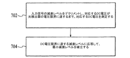
図7は、本発明による別の実施形態を示し、光ヘテロダイン検出システムの動作中に最小減衰レベルを求めるためのプロセス流れ図である。ブロック702において、入力信号の減衰レベルをデクリメントし、対応するDC電圧が光検出器の電圧限界に達するまで対応するDC電圧を測定する。ブロック704では、DC電圧限界に達する減衰レベルに応答して、最小減衰レベルが確立される。
FIG. 7 illustrates another embodiment according to the present invention, which is a process flow diagram for determining a minimum attenuation level during operation of an optical heterodyne detection system. At
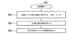
電源遮断時に、光検出器は予想される入力信号からの光パワーサージから保護されたままになるべきである。例えば、高いパワーの入力信号をシステムへ導入した場合、光検出器は損傷を受ける可能性がある。一実施形態では、光検出器の電源を落とす前に減衰レベルを最大減衰レベルに設定することにより、光検出器は光パワーサージから保護される。図8は、光ヘテロダイン検出システムの電源を落とすための技術のプロセス流れ図を示す。ブロック802では、システムは通常動作状態にある。電源遮断の開始時、ブロック804において減衰レベルは最大減衰レベルに設定される。減衰レベルを最大減衰レベルに設定した後、ブロック806において、光検出器の電源は遮断される。光検出器の電源を落とした後、ブロック808において、光ヘテロダイン検出システムの残りの部分の電源が、光検出器に損傷を与えることなく遮断され得る。
Upon power loss, the photodetector should remain protected from optical power surges from the expected input signal. For example, if a high power input signal is introduced into the system, the photodetector may be damaged. In one embodiment, the photodetector is protected from optical power surges by setting the attenuation level to the maximum attenuation level before powering down the photodetector. FIG. 8 shows a process flow diagram of a technique for powering down an optical heterodyne detection system. At
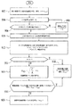
一実施形態では、減衰レベルは、光検出器の保護と信号対雑音比の改善の両方を達成するために制御され得る。特に、光検出器の飽和と損傷を防ぐために図5と図6に関連して説明されたように、一旦最小減衰レベル(αmax)を求めた後、信号対雑音比を改善するための減衰レベルの調整は、最小減衰レベルにより制限される。すなわち、減衰レベルが最小減衰レベルに、又はそれより上に維持される限り、減衰レベルを調整することによりヘテロダインビート信号の信号対雑音比は改善され得る。図9は、減衰レベルを制御してヘテロダインビート信号の信号対雑音比を改善するための技術のプロセス流れ図を示し、減衰の下側範囲は以前に確立された最小減衰レベル(すなわちαmax)によって制限される。ブロック902では、最小減衰レベルが入力信号に適用(すなわちαmax)され、そこでは最小減衰レベルは所定の値である。ブロック904では、出力信号Sは減衰された入力信号に応答して測定される。判断ブロック906では、出力信号の十分なサンプル測定値が得られたか否かが判断される。十分なサンプル測定値が存在しないと判定された場合、ブロック908において減衰レベルをインクリメントする。すなわち、入力信号に適用される減衰レベルは、いくらかの増分量だけ増大する。一実施形態では、減衰レベルは2〜7dBの間隔でインクリメントされるが、他の間隔を用いることもできる。減衰レベルをインクリメントした後、ブロック904において出力信号が再度測定される。
In one embodiment, the attenuation level may be controlled to achieve both protection of the photodetector and improved signal to noise ratio. In particular, once the minimum attenuation level (α max ) has been determined, as described in connection with FIGS. 5 and 6 to prevent photodetector saturation and damage, the attenuation to improve the signal-to-noise ratio Adjustment of the level is limited by the minimum attenuation level. That is, by adjusting the attenuation level, the signal-to-noise ratio of the heterodyne beat signal can be improved as long as the attenuation level is maintained at or above the minimum attenuation level. FIG. 9 shows a process flow diagram of a technique for controlling the attenuation level to improve the signal-to-noise ratio of the heterodyne beat signal, wherein the lower range of the attenuation is determined by the previously established minimum attenuation level (ie, α max ). Limited. At
判断ブロック906に戻り、十分なサンプル測定値があると判定された場合、ブロック910において出力信号の基礎測定値が得られる。一実施形態では、出力信号の基礎測定値は式αopt中のC項を求めるために使用される。C項が局部発振器信号及び受信器からの雑音の組み合わせを表わすため、基礎測定値は、局部発振器信号が存在し、かつ入力信号の無い状態で得られる。基礎測定値を得た後に、ブロック912において出力信号のサンプル測定値が出力信号対減衰曲線に当てはめられる。一実施形態では、サンプル測定値は、減衰の関数としての出力信号の二次多項式S(α)=Aα2+(B+D)α+Cに代入される。A項を求めた後、判断ブロック911において、Aがゼロ未満であるかどうかを判断する。Aがゼロ未満である場合、最小減衰レベルは先に確立された最小減衰レベル(すなわちαmax)に設定される。Aがゼロ未満でない場合、ブロック914において最適減衰レベルを下式から計算する:
αopt=√(C/A) (21)
Returning to decision block 906, if it is determined that there are sufficient sample measurements, a basic measurement of the output signal is obtained at
α opt = √ (C / A) (21)
判断ブロック916において、最適減衰レベルが以前に確立された最小減衰レベル未満かどうか判断される。最適減衰レベルが以前に確立された最小減衰レベル未満である場合、ブロック918において、減衰レベルは以前に確立された最小減衰レベルに設定される。すなわち、減衰レベルは、たとえより低い減衰レベルが信号対雑音比を改善するにしても、光検出器を保護するように以前に確立された最小減衰レベル未満に低下させてはならない。最適減衰レベルが最小減衰レベルを上回る場合、ブロック920において減衰レベルは最適減衰レベルに設定される。すなわち、最適減衰レベルが最小減衰レベルを上回る限り、減衰レベルは最適減衰レベルに設定される。
In
光ヘテロダイン検出システムの光学部品は、光ファイバにより接続されるものとして説明されたが、個々のデバイスはプレーナ型導波路回路のようなモノリシックデバイス上に集積化され得る。代案として、光学素子は自由空間により接続され得る。 Although the optical components of the optical heterodyne detection system have been described as being connected by optical fibers, individual devices can be integrated on a monolithic device such as a planar waveguide circuit. Alternatively, the optical elements can be connected by free space.
本明細書に記載された方法のステップ全てを実行したり、又は記載された順序で実行されなければならないことのないことは、認識されるべきである。 It should be appreciated that not all steps of the method described herein need to be performed or performed in the order described.
本発明による特定の実施形態を説明し図示してきたが、本発明は、説明され図示された特定の形態や部品の構成に限定されない。本発明は、特許請求の範囲によってのみ制限される。 Although specific embodiments according to the present invention have been described and illustrated, the invention is not limited to the specific forms and arrangements of components described and illustrated. The invention is limited only by the claims.
102 入力信号
104 入力ファイバ
105 局部発振器源
106 局部発振器信号
108 局部発振器ファイバ
110 光カプラ
112 光受信器
116 プロセッサ
118、120 出力ファイバ
124 減衰器
102 input signal
104 input fiber
105 Local oscillator source
106 Local oscillator signal
108 Local oscillator fiber
110 Optical coupler
112 optical receiver
116 processor
118, 120 output fiber
124 attenuator
Claims (10)
前記局部発振器信号に応答し、かつ前記入力信号の無い状態で前記出力信号の基礎測定値を取得(402)するステップと、
前記入力信号に応答し、異なる減衰レベルの関数として前記出力信号のサンプル測定値を取得(404)するステップと、及び
前記基礎測定値と前記サンプル測定値の関数として前記最適減衰レベルを求める(406)ステップとを含む、方法。 A method for determining an optimal attenuation level for an input signal (102) in an optical heterodyne detection system, wherein the optical heterodyne detection system combines the input signal with a local oscillator signal (106) to form a combined optical signal. An optical coupler (110) and a receiver (112) optically coupled to the optical coupler for generating an output signal in response to one of the input signal, the local oscillator signal, and the combined optical signal; ) And an attenuator (124) optically coupled to the optical coupler for attenuating the input signal, the method comprising:
Obtaining 402 a base measurement of the output signal in response to the local oscillator signal and in the absence of the input signal;
Obtaining (404) sample measurements of the output signal as a function of different attenuation levels in response to the input signal; and determining (406) the optimum attenuation level as a function of the base measurement and the sample measurements. ).
前記サンプル測定値から前記入力信号(102)の強度雑音特性を特定するステップと、及び
前記最適減衰レベルを求めるステップにおいて前記強度雑音特性を利用するステップとを含む、請求項1に記載の方法。 The step of determining (406) the optimum attenuation level includes:
The method of claim 1, comprising determining an intensity noise characteristic of the input signal (102) from the sample measurements; and utilizing the intensity noise characteristic in determining the optimal attenuation level.
αopt=√(C/A)
の関数として前記最適減衰レベルを求める(314)ステップを含む、請求項6に記載の方法。 Determining the optimal attenuation level,
α opt = √ (C / A)
The method of claim 6, comprising determining (314) the optimal attenuation level as a function of:
入力信号を減衰させるための調整可能な減衰器(124)と、
前記減衰器から前記入力信号を受信し、かつ局部発振器信号を受信するように結合された光カプラ(110)と、
前記光カプラからの合成光信号を受信するように結合された光受信器(112)と、及び
減衰制御モジュール(122)とを含み、
前記減衰制御モジュール(122)が、
前記局部発振器信号に応答し、かつ前記入力信号の無い状態で前記出力信号の基礎測定値を取得(402)し、
前記入力信号に応答し、異なる減衰レベルの関数として前記出力信号のサンプル測定値を取得(404)し、及び
前記基礎測定値と前記サンプル測定値の関数として前記減衰器に関する最適減衰レベルを求める(406)ように構成されている、光ヘテロダイン検出システム。 An optical heterodyne detection system,
An adjustable attenuator (124) for attenuating the input signal;
An optical coupler (110) coupled to receive the input signal from the attenuator and to receive a local oscillator signal;
An optical receiver (112) coupled to receive the combined optical signal from the optical coupler, and an attenuation control module (122);
The attenuation control module (122) includes:
Acquiring (402) a base measurement of the output signal in response to the local oscillator signal and in the absence of the input signal;
Responsive to the input signal, obtaining 404 sample measurements of the output signal as a function of different attenuation levels, and determining an optimal attenuation level for the attenuator as a function of the base measurements and the sample measurements (404). 406) An optical heterodyne detection system configured as described above.
前記サンプル測定値から前記入力信号(102)の強度雑音特性を特定することと、及び
前記最適減衰レベルを求めることにおいて前記強度雑音特性を利用することとを含む、請求項8に記載の光ヘテロダイン検出システム。
Determining the optimal attenuation level (406) comprises:
9. The optical heterodyne of claim 8, comprising: determining an intensity noise characteristic of the input signal (102) from the sample measurements; and utilizing the intensity noise characteristic in determining the optimal attenuation level. Detection system.
Applications Claiming Priority (1)
| Application Number | Priority Date | Filing Date | Title |
|---|---|---|---|
| US10/279,436 US7012697B2 (en) | 2002-10-24 | 2002-10-24 | Heterodyne based optical spectrum analysis with controlled optical attenuation |
Publications (2)
| Publication Number | Publication Date |
|---|---|
| JP2004147323A true JP2004147323A (en) | 2004-05-20 |
| JP2004147323A5 JP2004147323A5 (en) | 2006-12-07 |
Family
ID=32106712
Family Applications (1)
| Application Number | Title | Priority Date | Filing Date |
|---|---|---|---|
| JP2003360135A Pending JP2004147323A (en) | 2002-10-24 | 2003-10-21 | Heterodyne-based optical spectrum analysis of using controlled optical attenuation |
Country Status (2)
| Country | Link |
|---|---|
| US (1) | US7012697B2 (en) |
| JP (1) | JP2004147323A (en) |
Cited By (8)
| Publication number | Priority date | Publication date | Assignee | Title |
|---|---|---|---|---|
| JP2009212994A (en) * | 2008-03-06 | 2009-09-17 | Nec Corp | Coherent optical receiver and adjustment method thereof |
| JP2010210541A (en) * | 2009-03-12 | 2010-09-24 | Anritsu Corp | Optical heterodyne spectrum analyzer |
| JP2010245772A (en) * | 2009-04-03 | 2010-10-28 | Fujitsu Ltd | Optical receiver and method for optical reception |
| JP2012042380A (en) * | 2010-08-20 | 2012-03-01 | Anritsu Corp | Optical spectrum analyzer |
| JP2012521118A (en) * | 2009-03-19 | 2012-09-10 | アジレント・テクノロジーズ・インク | Optical downconverter calibration |
| JP2013046162A (en) * | 2011-08-23 | 2013-03-04 | Nec Corp | Coherent optical reception device and coherent optical reception method |
| JP2013081186A (en) * | 2011-04-15 | 2013-05-02 | Nec Corp | Coherent receiver |
| WO2019012818A1 (en) * | 2017-07-14 | 2019-01-17 | 日本電気株式会社 | Pluggable optical module, optical communication system, and method for controlling pluggable optical module |
Families Citing this family (5)
| Publication number | Priority date | Publication date | Assignee | Title |
|---|---|---|---|---|
| US7012697B2 (en) * | 2002-10-24 | 2006-03-14 | Agilent Technologies, Inc. | Heterodyne based optical spectrum analysis with controlled optical attenuation |
| JP5852300B2 (en) * | 2009-12-02 | 2016-02-03 | オリンパス株式会社 | Photodetector, microscope and endoscope |
| US9166700B2 (en) * | 2010-03-21 | 2015-10-20 | Alcatel Lucent | Tunable receiver |
| JP5686142B2 (en) * | 2011-01-20 | 2015-03-18 | 日本電気株式会社 | Coherent light receiving apparatus and coherent light receiving method |
| CN107733641B (en) * | 2017-08-29 | 2020-12-22 | 上海循态信息科技有限公司 | High-speed high-adjustable-bandwidth quantum balance homodyne detector and control method thereof |
Family Cites Families (4)
| Publication number | Priority date | Publication date | Assignee | Title |
|---|---|---|---|---|
| US4856899A (en) | 1985-12-20 | 1989-08-15 | Yokogawa Electric Corporation | Optical frequency analyzer using a local oscillator heterodyne detection of incident light |
| DE4244605A1 (en) | 1992-05-27 | 1993-12-02 | Hewlett Packard Co | Optical low-coherence reflectometer with improved sensitivity with optical attenuation |
| US6600594B1 (en) * | 2002-02-21 | 2003-07-29 | Lightech Fiberoptics, Inc. | Intelligent variable optical attenuator with controller and attenuation calibration |
| US7012697B2 (en) * | 2002-10-24 | 2006-03-14 | Agilent Technologies, Inc. | Heterodyne based optical spectrum analysis with controlled optical attenuation |
-
2002
- 2002-10-24 US US10/279,436 patent/US7012697B2/en not_active Expired - Fee Related
-
2003
- 2003-10-21 JP JP2003360135A patent/JP2004147323A/en active Pending
Cited By (14)
| Publication number | Priority date | Publication date | Assignee | Title |
|---|---|---|---|---|
| JP4518282B2 (en) * | 2008-03-06 | 2010-08-04 | 日本電気株式会社 | Coherent optical receiver and adjustment method thereof |
| JP2009212994A (en) * | 2008-03-06 | 2009-09-17 | Nec Corp | Coherent optical receiver and adjustment method thereof |
| US8078064B2 (en) | 2008-03-06 | 2011-12-13 | Nec Corporation | Coherent optical receiver and adjustment method thereof |
| JP2010210541A (en) * | 2009-03-12 | 2010-09-24 | Anritsu Corp | Optical heterodyne spectrum analyzer |
| JP2012521118A (en) * | 2009-03-19 | 2012-09-10 | アジレント・テクノロジーズ・インク | Optical downconverter calibration |
| JP2010245772A (en) * | 2009-04-03 | 2010-10-28 | Fujitsu Ltd | Optical receiver and method for optical reception |
| JP2012042380A (en) * | 2010-08-20 | 2012-03-01 | Anritsu Corp | Optical spectrum analyzer |
| JP2013081186A (en) * | 2011-04-15 | 2013-05-02 | Nec Corp | Coherent receiver |
| JP2013046162A (en) * | 2011-08-23 | 2013-03-04 | Nec Corp | Coherent optical reception device and coherent optical reception method |
| WO2019012818A1 (en) * | 2017-07-14 | 2019-01-17 | 日本電気株式会社 | Pluggable optical module, optical communication system, and method for controlling pluggable optical module |
| JPWO2019012818A1 (en) * | 2017-07-14 | 2020-06-11 | 日本電気株式会社 | Pluggable optical module, optical communication system, and pluggable optical module control method |
| US10917172B2 (en) | 2017-07-14 | 2021-02-09 | Nec Corporation | Pluggable optical module, optical communication system, and control method of pluggable optical module |
| JP6996559B2 (en) | 2017-07-14 | 2022-01-17 | 日本電気株式会社 | Control method of pluggable optical module, optical communication system and pluggable optical module |
| US11342991B2 (en) | 2017-07-14 | 2022-05-24 | Nec Corporation | Pluggable optical module, optical communication system, and control method of pluggable optical module |
Also Published As
| Publication number | Publication date |
|---|---|
| US7012697B2 (en) | 2006-03-14 |
| US20040080753A1 (en) | 2004-04-29 |
Similar Documents
| Publication | Publication Date | Title |
|---|---|---|
| Baney et al. | Theory and measurement techniques for the noise figure of optical amplifiers | |
| US6008935A (en) | Optical amplifier and optical amplifier gain control method and apparatus | |
| US7012697B2 (en) | Heterodyne based optical spectrum analysis with controlled optical attenuation | |
| US6259529B1 (en) | Wavelength-selective polarization-diverse optical heterodyne receiver | |
| US6515276B2 (en) | Heterodyne optical spectrum analyzer with provisions for intensity noise subtraction | |
| US6678041B2 (en) | Optical characteristic measuring apparatus, the method thereof and recording medium | |
| US6486958B1 (en) | Method and system for optical spectrum analysis with matched filter detection | |
| US6256103B1 (en) | System and method for optical heterodyne detection of an optical signal | |
| US6317214B1 (en) | Method and apparatus to determine a measurement of optical multiple path interference | |
| US6970250B1 (en) | Method and system for optical heterodyne detection of an optical signal that utilizes optical attenuation | |
| US6535289B1 (en) | System and method for optical heterodyne detection of an optical signal | |
| US6590666B2 (en) | Method and system for optical spectrum analysis with non-uniform sweep rate correction | |
| EP0486205B1 (en) | Method and apparatus for determining the absolute noise figure of optical amplifiers | |
| US6646746B1 (en) | Method and system for optical heterodyne detection of an optical signal | |
| US5700949A (en) | Optical receiver calibration based on a relative intensity noise standard | |
| JP3403643B2 (en) | Polarization-dependent precision measurement equipment | |
| KR20000051885A (en) | Dispersion value measurement system of optical fiber | |
| Rutkowski et al. | Miteq DR-125G-A, 12-GHZ Fiber-Optic Detector Evaluations for Photonic Doppler Velocimetry Diagnostic | |
| JP2003249895A (en) | Logarithmic conversion circuit, optical detection circuit, and optical amplifier | |
| Stolze et al. | Optical all-loss test solution | |
| JP2006170976A (en) | Device and method for setting incidence light power ratio, program, and recording medium | |
| Shadaram et al. | RF phase noise in WDM fiber optic links | |
| GB2370109A (en) | Optical wavelength meter | |
| Chennu et al. | Performance Evaluation of WDM Fiber Optic Frequency Distribution Systems |
Legal Events
| Date | Code | Title | Description |
|---|---|---|---|
| A521 | Request for written amendment filed |
Free format text: JAPANESE INTERMEDIATE CODE: A523 Effective date: 20061020 |
|
| A621 | Written request for application examination |
Free format text: JAPANESE INTERMEDIATE CODE: A621 Effective date: 20061020 |
|
| A131 | Notification of reasons for refusal |
Free format text: JAPANESE INTERMEDIATE CODE: A131 Effective date: 20071225 |
|
| A02 | Decision of refusal |
Free format text: JAPANESE INTERMEDIATE CODE: A02 Effective date: 20080527 |