JP2004140885A - Switching regulator circuit - Google Patents
Switching regulator circuit Download PDFInfo
- Publication number
- JP2004140885A JP2004140885A JP2002300960A JP2002300960A JP2004140885A JP 2004140885 A JP2004140885 A JP 2004140885A JP 2002300960 A JP2002300960 A JP 2002300960A JP 2002300960 A JP2002300960 A JP 2002300960A JP 2004140885 A JP2004140885 A JP 2004140885A
- Authority
- JP
- Japan
- Prior art keywords
- voltage
- low
- switching regulator
- coil
- passive element
- Prior art date
- Legal status (The legal status is an assumption and is not a legal conclusion. Google has not performed a legal analysis and makes no representation as to the accuracy of the status listed.)
- Pending
Links
- 230000005669 field effect Effects 0.000 claims description 19
- 238000009499 grossing Methods 0.000 claims description 14
- 238000001514 detection method Methods 0.000 claims description 9
- 239000003990 capacitor Substances 0.000 description 5
- 230000007423 decrease Effects 0.000 description 2
Images
Classifications
-
- H—ELECTRICITY
- H02—GENERATION; CONVERSION OR DISTRIBUTION OF ELECTRIC POWER
- H02M—APPARATUS FOR CONVERSION BETWEEN AC AND AC, BETWEEN AC AND DC, OR BETWEEN DC AND DC, AND FOR USE WITH MAINS OR SIMILAR POWER SUPPLY SYSTEMS; CONVERSION OF DC OR AC INPUT POWER INTO SURGE OUTPUT POWER; CONTROL OR REGULATION THEREOF
- H02M3/00—Conversion of dc power input into dc power output
- H02M3/02—Conversion of dc power input into dc power output without intermediate conversion into ac
- H02M3/04—Conversion of dc power input into dc power output without intermediate conversion into ac by static converters
- H02M3/10—Conversion of dc power input into dc power output without intermediate conversion into ac by static converters using discharge tubes with control electrode or semiconductor devices with control electrode
- H02M3/145—Conversion of dc power input into dc power output without intermediate conversion into ac by static converters using discharge tubes with control electrode or semiconductor devices with control electrode using devices of a triode or transistor type requiring continuous application of a control signal
- H02M3/155—Conversion of dc power input into dc power output without intermediate conversion into ac by static converters using discharge tubes with control electrode or semiconductor devices with control electrode using devices of a triode or transistor type requiring continuous application of a control signal using semiconductor devices only
- H02M3/156—Conversion of dc power input into dc power output without intermediate conversion into ac by static converters using discharge tubes with control electrode or semiconductor devices with control electrode using devices of a triode or transistor type requiring continuous application of a control signal using semiconductor devices only with automatic control of output voltage or current, e.g. switching regulators
Abstract
Description
【0001】
【発明の属する技術分野】
本発明は、負荷に供給する電力をコントロールするスイッチングレギュレータ回路に関する。
【0002】
【従来の技術】
従来、負荷に供給する電力をコントロールするために、電源と負荷との間にスイッチングレギュレータ回路が設けられている。スイッチングレギュレータ回路は、負荷と直列に設けられたコイルに電力を供給するか否かを繰り返し切り替えることにより、負荷に供給する電圧及び電流を制御する(例えば、特許文献1参照)。
【0003】
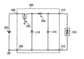
図1に、従来のスイッチングレギュレータ回路300を示す。スイッチングレギュレータ回路300は、電源200と負荷250との間に設けられる。スイッチングレギュレータ回路300は、高圧入力端子306、低圧入力端子308、高圧出力端子310、低圧出力端子312、スイッチング素子302、整流ダイオード314、平滑コンデンサ316、及びコイル304を備える。
【0004】
高圧入力端子306は、電源200の高圧端子と接続され、低圧入力端子308は、電源200の低圧端子と接続される。また、高圧出力端子310は、負荷250の高圧端子と接続され、低圧出力端子312は、負荷250の低圧端子と接続される。
【0005】
コイル304は、高圧入力端子306と高圧出力端子310との間に直列に設けられ、スイッチング素子302はコイル304と高圧入力端子306との間に直列に設けられる。スイッチング素子302は、オンオフを繰り返すことにより、負荷250に電源電圧より低い電圧を供給する。つまり、スイッチング素子302がオン状態となった場合、電源200からコイル304に電流が供給され、スイッチング素子302がオフ状態に切り替わった場合、整流ダイオード314を介してコイル304に電流が供給される。スイッチング素子302がオフ状態となった場合、電源200からコイル304に供給される電流が零に減少するため、コイル304は当該減少を補償するために、負荷250に供給された電流を整流ダイオード314を介して受け取る。このため、負荷250には、直流的な電流が供給される。
【0006】
従来、スイッチング素子302として、電界効果トランジスタが用いられているが、スイッチング素子302は、高圧入力端子306と高圧出力端子310との間に設けられているため、pチャネル電界効果トランジスタを用いる必要がある。つまり、nチャネル電界効果トランジスタを用いた場合、ゲート端子に電源電圧より高い電圧を印加する必要があるため、使用することが困難であった。
【0007】
【特許文献1】
特開2001−215913号公報(第6−12頁、第2−6図)
【0008】
【発明が解決しようとする課題】
従来のスイッチングレギュレータ回路300は、スイッチング素子302としてpチャネル電界効果トランジスタを用いているため、所定の耐圧、及び所定のオン抵抗を有するスイッチング素子302を用いようとした場合、チップ面積が大きくなってしまう恐れがある。また、pチャネル電界効果トランジスタは、キャリアの移動度が低いため、高速に動作させることが困難である。
【0009】
また、pチャネル電界効果トランジスタは、市場に流通している種類が少ないため、所望の特性を有するpチャネル電界効果トランジスタを選定することが困難である。
【0010】
【課題を解決するための手段】
上記課題を解決するために、本発明の第1の形態においては、与えられた2つの入力電位の接地電位に対する電位差によらず、2つの入力電位の電位差により駆動する受動素子に、2つの入力電位を供給するスイッチングレギュレータ回路であって、2つの入力電位のうち低い低入力電位を受け取る低圧入力端子と、低圧入力端子と受動素子との間に直列に設けられたコイルと、低圧入力端子と受動素子との間に、コイルと直列に設けられ、コイルに電流を流すか否かを繰り返し切り替えることにより、コイルに低入力電位より高い電位を生成させ、受動素子に供給するスイッチング素子とを備えることを特徴とするスイッチングレギュレータ回路を提供する。
【0011】
また、スイッチング素子は、コイルと直列に設けられたnチャネル電界効果トランジスタであって、スイッチングレギュレータ回路は、スイッチングレギュレータ回路から受動素子に供給される供給電圧又は供給電流を検出する検出部と、検出部が検出した供給電圧又は供給電流に基づいて、nチャネル電界効果トランジスタのゲートに印加する電圧を制御することにより、nチャネル電界効果トランジスタがオン又はオフとなる時間比を制御する制御部を更に備えてよい。
【0012】
また、受動素子は、与えられた電位差に基づいて発光する発光ダイオードであってよい。また、スイッチングレギュレータ回路は、受動素子に与えられる電位差の変化を平滑にする平滑フィルタを更に備えてよい。また、2つの入力電位のうち高い高入力電位を受け取る高圧入力端子と、高圧入力端子と受動素子との間に直列に設けられ、高圧入力端子から受動素子へ順方向電流を供給するダイオードとを更に備えてよい。
【0013】
尚、上記の発明の概要は、本発明の必要な特徴の全てを列挙したものではなく、これらの特徴群のサブコンビネーションも又、発明となりうる。
【0014】
【発明の実施の形態】
以下、発明の実施の形態を通じて本発明を説明するが、以下の実施形態は特許請求の範囲にかかる発明を限定するものではなく、又実施形態の中で説明されている特徴の組み合わせの全てが発明の解決手段に必須であるとは限らない。
【0015】
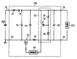
図2は、本発明の実施形態に係るスイッチングレギュレータ回路100の構成の一例を示す。スイッチングレギュレータ回路100は、電源200から与えられた電力に応じて、負荷250に電力を供給する。本例において、負荷250は、与えられた2つの入力電位の接地電位に対する電位差によらず、2つの入力電位の電位差により駆動する受動素子である。例えば、負荷250は、与えられた電位差に基づいて発光する発光ダイオードである。
【0016】
スイッチングレギュレータ回路100は、高圧入力端子52、低圧入力端子54、高圧出力端子56、低圧出力端子58、ノイズフィルタ12、整流素子14、平滑フィルタ16、整流素子18、平滑フィルタ20、検出部30、スイッチング素子22、コイル24、及び制御部40を備える。
【0017】
高圧入力端子52は、電源200の高圧端子に接続され高入力電位を受け取り、低圧入力端子54は、電源200の低圧端子に接続され、高入力電位より低い低入力電位を受け取る。
【0018】
ノイズフィルタ12及び整流素子14は、高圧入力端子52と、負荷250の高圧端子に接続される高圧出力端子56との間に直列に設けられる。ノイズフィルタ12は、例えばコイルであって、高圧入力端子52から高圧出力端子56に伝送される高入力電位の高周波ノイズを除去する。また、整流素子14は、例えばダイオードであって、高圧入力端子52と高圧出力端子56との間に直列に設けられ、高圧入力端子52から高圧出力端子56へ順方向電流を供給する。
【0019】
コイル24は、低圧入力端子54と、負荷250の低圧端子に接続される低圧出力端子58との間に直列に設けられる。スイッチング素子22は、低圧入力端子54と低圧出力端子58との間に、コイル24と直列に設けられ、コイル24に電流を流すか否かを繰り返し切り替えることにより、コイル24に低入力電位より高い電位を生成させ、低圧出力端子58を介して負荷250の低圧端子に供給する。
【0020】
また、スイッチング素子22は、コイル24と直列に設けられたnチャネル電界効果トランジスタである。つまり、スイッチング素子22のソース端子は低圧入力端子54に接続され、ドレイン端子は低圧出力端子58に接続される。
【0021】
検出部30は、スイッチングレギュレータ回路100から負荷250に供給される供給電圧又は供給電流を検出する。例えば、検出部30は、高圧出力端子56と低圧出力端子58との電位差を、供給電圧として検出してよい。
【0022】
制御部40は、検出部30が検出した供給電圧又は供給電流に基づいて、スイッチング素子22のゲートに印加する電圧を制御することにより、スイッチング素子22がオン又はオフとなる前記時間比を制御する。これにより、負荷250に供給される供給電圧及び供給電流を略一定の値に制御することができる。
【0023】
本例におけるスイッチングレギュレータ回路100によれば、低圧側にスイッチング素子22を設けているため、スイッチング素子22としてnチャネル電界効果トランジスタを用いることができる。つまり、低圧入力端子54が接地されているため、スイッチング素子22としてnチャネル電界効果トランジスタを用いてスイッチング動作させる場合、接地電位に対して所定の閾電圧だけ高い電圧をゲート端子に印加すればよい。このため、電源200の電源電圧より低い電圧で、スイッチング素子22を制御することができる。
【0024】
本例におけるスイッチングレギュレータ回路100は、スイッチング素子22としてnチャネル電界効果トランジスタを用いているため、スイッチング素子22のチップ面積を小さくすることができる。また、高速にスイッチング動作させることができる。このため、スイッチング動作を高速化するための回路が必要ない。また、nチャネル電界効果トランジスタは、市場に流通している種類が多いため、所望の特性を有するpチャネル電界効果トランジスタを選定することができる。
【0025】
平滑フィルタ16は、高圧入力端子52から入力された電位のノイズを除去するフィルタである。平滑フィルタ16は、例えば整流素子14のカソード端子とスイッチング素子22のソース端子との間に、電源200と並列に設けられたコンデンサである。
【0026】
また、整流素子18は、図1において説明した整流ダイオード314と同様に、スイッチング素子22がオフ状態となった場合に、コイル24に電流を供給するために設けられる。つまり、整流素子18は、スイッチング素子22がオン状態のときにコイル24に流れた電流が、スイッチング素子22がオフ状態に切り替わった場合に流れる経路となる。整流素子18は、例えば整流素子14のカソード端子とスイッチング素子22のドレイン端子との間に、平滑フィルタ16と並列に設けられたダイオードである。
【0027】
平滑フィルタ20は、負荷250に与えられる電位差の変化を平滑にする。平滑フィルタ20は、例えば高圧出力端子56と低圧出力端子58との間に、負荷250と並列に設けられたコンデンサである。これにより、負荷250に与えられる電位差の急激な変動を制限することができる。
【0028】
また、検出部30は、シャント抵抗34、トランジスタ32、及びツェナダイオード36を有する。本例における検出部30は、負荷250に与えられる電位差を検出する。
【0029】
シャント抵抗34は、一端が高圧出力端子56と接続されており、他端がツェナダイオード36のカソード端子に接続される。また、ツェナダイオード36のアノード端子は、低圧出力端子58に接続され、シャント抵抗34及びツェナダイオード36は、負荷250と並列に設けられる。トランジスタ32のエミッタ端子は、高圧出力端子56と接続されており、ベース端子はシャント抵抗34の当該他端及びツェナダイオード36のカソード端子に接続される。また、トランスタ32は、コレクタ電流を制御部40に供給する。
【0030】
負荷250に与えられる電位差が、ツェナダイオード36の逆方向閾電圧より小さい場合、トランジスタ32はオフ状態となり、制御部40にはコレクタ電流が供給されない。この場合、制御部40は、スイッチング素子22のオンデューティー比を増加させ、負荷250に与えられる電位差を増加させる。
【0031】
また、負荷250に与えられる電位差が、ツェナダイオード36の逆方向閾電圧より大きい場合、トランジスタ32はオン状態となる。負荷250に与えられる電位差が更に増大した場合、シャント抵抗34における降下電圧が増大するため、制御部40に供給されるコレクタ電流も増大する。この場合、制御部40は、スイッチング素子22のオンデューティーを減少させ、負荷250に与えられる電位差を減少させる。これにより、負荷250に与えられる電位差を、ツェナダイオード36の逆方向閾電圧とトランジスタ32のベースエミッタ間電圧との和と等しくなるように制御することができる。
【0032】
また、本例においてはコイル24は、低圧入力端子54と低圧出力端子58との間に設けられていたが、他の例においてはコイル24は、高圧入力端子52と高圧出力端子56との間に直列に設けられていてもよい。このような構成によっても、スイッチング素子22のデューティー比を制御することにより、負荷250に与えられる電位差を制御することができる。
【0033】
以上、本発明を実施の形態を用いて説明したが、本発明の技術的範囲は上記実施の形態に記載の範囲には限定されない。上記実施の形態に、多様な変更又は改良を加えることが可能であることが当業者に明らかである。その様な変更又は改良を加えた形態も本発明の技術的範囲に含まれ得ることが、特許請求の範囲の記載から明らかである。
【0034】
上記説明から明らかなように、本発明によれば、小さい回路規模で高速にスイッチング動作することのできるスイッチングレギュレータ回路を提供することができる。
【図面の簡単な説明】
【図1】従来のスイッチングレギュレータ回路300を示す。
【図2】図2は、本発明の実施形態に係るスイッチングレギュレータ回路100の構成の一例を示す。
【符号の説明】
12・・・ノイズフィルタ、14・・・整流素子、16・・・平滑フィルタ、18・・・整流素子、20・・・平滑フィルタ、22・・・スイッチング素子、24・・・コイル、30・・・検出部、32・・・トランジスタ、36・・・ツェナーダイオード、40・・・制御部、52・・・高圧入力端子、54・・・低圧入力端子、56・・・高圧出力端子、58・・・低圧出力端子、100・・・スイッチングレギュレータ回路、200・・・電源、250・・・負荷、300・・・スイッチングレギュレータ回路、302・・・スイッチング素子、304・・・コイル、306・・・高圧入力端子、308・・・低圧入力端子、310・・・高圧出力端子、312・・・低圧出力端子、314・・・整流ダイオード、316・・・平滑コンデンサ[0001]
TECHNICAL FIELD OF THE INVENTION
The present invention relates to a switching regulator circuit that controls power supplied to a load.
[0002]
[Prior art]
Conventionally, a switching regulator circuit is provided between a power supply and a load in order to control power supplied to the load. The switching regulator circuit controls the voltage and current supplied to the load by repeatedly switching whether or not to supply power to a coil provided in series with the load (for example, see Patent Document 1).
[0003]
FIG. 1 shows a conventional
[0004]
The high
[0005]
The
[0006]
Conventionally, a field effect transistor is used as the
[0007]
[Patent Document 1]
JP-A-2001-215913 (pages 6-12, FIG. 2-6)
[0008]
[Problems to be solved by the invention]
Since the conventional
[0009]
Further, since there are few types of p-channel field-effect transistors on the market, it is difficult to select a p-channel field-effect transistor having desired characteristics.
[0010]
[Means for Solving the Problems]
In order to solve the above-mentioned problem, in a first embodiment of the present invention, a passive element driven by a potential difference between two input potentials is connected to two input potentials irrespective of a potential difference between a given two input potentials and a ground potential. A switching regulator circuit that supplies a potential, a low-voltage input terminal that receives a low low input potential of the two input potentials, a coil provided in series between the low-voltage input terminal and the passive element, and a low-voltage input terminal. A switching element that is provided in series with the coil between the passive element and the coil to generate a potential higher than a low input potential by repeatedly switching whether or not a current flows through the coil and supplies the potential to the passive element; A switching regulator circuit is provided.
[0011]
The switching element is an n-channel field-effect transistor provided in series with the coil, and the switching regulator circuit includes a detection unit that detects a supply voltage or a supply current supplied from the switching regulator circuit to the passive element. A control unit that controls a time ratio at which the n-channel field-effect transistor is turned on or off by controlling a voltage applied to the gate of the n-channel field-effect transistor based on the supply voltage or the supply current detected by the unit. May be provided.
[0012]
In addition, the passive element may be a light emitting diode that emits light based on a given potential difference. The switching regulator circuit may further include a smoothing filter for smoothing a change in a potential difference applied to the passive element. Also, a high-voltage input terminal that receives a high input potential higher than the two input potentials, and a diode that is provided in series between the high-voltage input terminal and the passive element and supplies a forward current from the high-voltage input terminal to the passive element Further provision may be made.
[0013]
Note that the above summary of the present invention does not list all of the necessary features of the present invention, and a sub-combination of these features may also be an invention.
[0014]
BEST MODE FOR CARRYING OUT THE INVENTION
Hereinafter, the present invention will be described through embodiments of the present invention. However, the following embodiments do not limit the invention according to the claims, and all of the combinations of the features described in the embodiments are not limited thereto. It is not always essential to the solution of the invention.
[0015]
FIG. 2 shows an example of a configuration of the
[0016]
The
[0017]
The high voltage input terminal 52 is connected to a high voltage terminal of the
[0018]
The
[0019]
The
[0020]
The switching
[0021]
The
[0022]
The
[0023]
According to the
[0024]
Since the
[0025]
The smoothing
[0026]
The rectifying
[0027]
The smoothing
[0028]
The
[0029]
One end of the
[0030]
When the potential difference applied to the
[0031]
When the potential difference applied to the
[0032]
In the present embodiment, the
[0033]
As described above, the present invention has been described using the embodiments, but the technical scope of the present invention is not limited to the scope described in the above embodiments. It is apparent to those skilled in the art that various changes or improvements can be made to the above embodiment. It is apparent from the description of the appended claims that embodiments with such changes or improvements can be included in the technical scope of the present invention.
[0034]
As is clear from the above description, according to the present invention, it is possible to provide a switching regulator circuit capable of performing a high-speed switching operation with a small circuit scale.
[Brief description of the drawings]
FIG. 1 shows a conventional
FIG. 2 shows an example of a configuration of a
[Explanation of symbols]
12 noise filter, 14 rectifier, 16 smoothing filter, 18 rectifier, 20 smoothing filter, 22 switching element, 24 coil, 30 coil ..Detection unit, 32 transistor, 36 Zener diode, 40 control unit, 52 high-voltage input terminal, 54 low-voltage input terminal, 56 high-voltage output terminal, 58 ... Low voltage output terminal, 100 ... Switching regulator circuit, 200 ... Power supply, 250 ... Load, 300 ... Switching regulator circuit, 302 ... Switching element, 304 ... Coil, 306 ..High voltage input terminal, 308 ・ ・ ・ Low voltage input terminal, 310 ・ ・ ・ High voltage output terminal, 312 ・ ・ ・ Low voltage output terminal, 314 ・ ・ ・ Rectifier diode, 316 ・ ・ ・ Smoothing capacitor Capacitors
Claims (5)
前記2つの入力電位のうち低い低入力電位を受け取る低圧入力端子と、
前記低圧入力端子と前記受動素子との間に直列に設けられたコイルと、
前記低圧入力端子と前記受動素子との間に、前記コイルと直列に設けられ、前記コイルに電流を流すか否かを繰り返し切り替えることにより、前記コイルに前記低入力電位より高い電位を生成させ、前記受動素子に供給するスイッチング素子と
を備えることを特徴とするスイッチングレギュレータ回路。A switching regulator circuit that supplies the two input potentials to a passive element driven by the potential difference between the two input potentials, regardless of a potential difference between the applied two input potentials and a ground potential,
A low voltage input terminal for receiving a low low input potential of the two input potentials;
A coil provided in series between the low-voltage input terminal and the passive element,
Between the low-voltage input terminal and the passive element, provided in series with the coil, by repeatedly switching whether or not to flow a current to the coil, to cause the coil to generate a potential higher than the low input potential, A switching element for supplying the passive element.
前記スイッチングレギュレータ回路は、
前記スイッチングレギュレータ回路から前記受動素子に供給される供給電圧又は供給電流を検出する検出部と、
前記検出部が検出した前記供給電圧又は供給電流に基づいて、前記nチャネル電界効果トランジスタのゲートに印加する電圧を制御することにより、前記nチャネル電界効果トランジスタがオン又はオフとなる前記時間比を制御する制御部を更に備えることを特徴とする請求項1に記載のスイッチングレギュレータ回路。The switching element is an n-channel field effect transistor provided in series with the coil,
The switching regulator circuit,
A detection unit that detects a supply voltage or a supply current supplied to the passive element from the switching regulator circuit,
By controlling a voltage applied to the gate of the n-channel field-effect transistor based on the supply voltage or the supply current detected by the detection unit, the time ratio at which the n-channel field-effect transistor is turned on or off is determined. The switching regulator circuit according to claim 1, further comprising a control unit for controlling.
前記高圧入力端子と前記受動素子との間に直列に設けられ、前記高圧入力端子から前記受動素子へ順方向電流を供給するダイオードと
を更に備えることを特徴とする請求項1に記載のスイッチングレギュレータ回路。A high-voltage input terminal for receiving a high high input potential of the two input potentials;
The switching regulator according to claim 1, further comprising: a diode provided in series between the high-voltage input terminal and the passive element, for supplying a forward current from the high-voltage input terminal to the passive element. circuit.
Priority Applications (2)
| Application Number | Priority Date | Filing Date | Title |
|---|---|---|---|
| JP2002300960A JP2004140885A (en) | 2002-10-15 | 2002-10-15 | Switching regulator circuit |
| US10/682,049 US6930472B2 (en) | 2002-10-15 | 2003-10-09 | Switching regulator circuit |
Applications Claiming Priority (1)
| Application Number | Priority Date | Filing Date | Title |
|---|---|---|---|
| JP2002300960A JP2004140885A (en) | 2002-10-15 | 2002-10-15 | Switching regulator circuit |
Publications (1)
| Publication Number | Publication Date |
|---|---|
| JP2004140885A true JP2004140885A (en) | 2004-05-13 |
Family
ID=32064255
Family Applications (1)
| Application Number | Title | Priority Date | Filing Date |
|---|---|---|---|
| JP2002300960A Pending JP2004140885A (en) | 2002-10-15 | 2002-10-15 | Switching regulator circuit |
Country Status (2)
| Country | Link |
|---|---|
| US (1) | US6930472B2 (en) |
| JP (1) | JP2004140885A (en) |
Cited By (1)
| Publication number | Priority date | Publication date | Assignee | Title |
|---|---|---|---|---|
| DE102015217712A1 (en) | 2014-09-16 | 2016-03-17 | Koito Manufacturing Co., Ltd. | Lighting circuit and vehicle lamp having such |
Families Citing this family (2)
| Publication number | Priority date | Publication date | Assignee | Title |
|---|---|---|---|---|
| KR100599708B1 (en) | 2004-05-25 | 2006-07-13 | 삼성에스디아이 주식회사 | Plasma display panel |
| JP5148452B2 (en) * | 2008-10-22 | 2013-02-20 | 三菱重工業株式会社 | Inductor drive circuit |
Family Cites Families (1)
| Publication number | Priority date | Publication date | Assignee | Title |
|---|---|---|---|---|
| JP2001215913A (en) | 2000-02-04 | 2001-08-10 | Toko Inc | Lighting circuit |
-
2002
- 2002-10-15 JP JP2002300960A patent/JP2004140885A/en active Pending
-
2003
- 2003-10-09 US US10/682,049 patent/US6930472B2/en not_active Expired - Fee Related
Cited By (5)
| Publication number | Priority date | Publication date | Assignee | Title |
|---|---|---|---|---|
| DE102015217712A1 (en) | 2014-09-16 | 2016-03-17 | Koito Manufacturing Co., Ltd. | Lighting circuit and vehicle lamp having such |
| DE102015217712B4 (en) * | 2014-09-16 | 2017-01-19 | Koito Manufacturing Co., Ltd. | Lighting circuit and vehicle lamp having such |
| US9907151B2 (en) | 2014-09-16 | 2018-02-27 | Koito Manufacturing Co., Ltd. | Lighting circuit and vehicle lamp having the same |
| US10420196B2 (en) | 2014-09-16 | 2019-09-17 | Koito Manufacturing Co., Ltd. | Lighting circuit and vehicle lamp having the same |
| DE102015017153B3 (en) | 2014-09-16 | 2023-10-26 | Koito Manufacturing Co., Ltd. | Lighting circuit and vehicle light having one |
Also Published As
| Publication number | Publication date |
|---|---|
| US6930472B2 (en) | 2005-08-16 |
| US20040070374A1 (en) | 2004-04-15 |
Similar Documents
| Publication | Publication Date | Title |
|---|---|---|
| US6563726B1 (en) | Synchronous bridge rectifier | |
| JP6209205B2 (en) | System and apparatus for driver circuit for protection of GaN FET gate | |
| US7746156B1 (en) | Circuit and method for driving a junction field effect transistor | |
| US7579880B2 (en) | Circuit for driving a semiconductor element | |
| US9468048B2 (en) | Input current regulator, driving method thereof, and disable circuit thereof | |
| US7551004B2 (en) | Inverter apparatus with improved gate drive for power MOSFET | |
| JP7066876B2 (en) | Self-biased ideal diode circuit | |
| EP2745368B1 (en) | Start-up circuit | |
| US6949889B2 (en) | Wide input voltage range light emitting diode driver | |
| JP2990133B2 (en) | Switching power supply circuit | |
| JP2009075957A (en) | Power circuit and semiconductor device | |
| US20130200867A1 (en) | High side driver circuitry | |
| JP2012043768A (en) | Novel led driver controller | |
| US8525499B2 (en) | Constant current switching power supply | |
| JP6652561B2 (en) | Adaptive controller for voltage converter | |
| JP2004140885A (en) | Switching regulator circuit | |
| CN214101190U (en) | Electronic circuit device | |
| JP3996147B2 (en) | Bootstrap capacitor charging circuit using a small charging current | |
| US7166932B2 (en) | Power circuit | |
| EP3528237A1 (en) | Current correction techniques for accurate high current short channel driver | |
| JP2002374672A (en) | Switching power source apparatus | |
| JP2000184695A (en) | Power supply device | |
| JP6164129B2 (en) | Lighting circuit and lighting device | |
| JP2004519190A (en) | Switching power supply | |
| JP2011147202A (en) | Switching power unit |
Legal Events
| Date | Code | Title | Description |
|---|---|---|---|
| A621 | Written request for application examination |
Free format text: JAPANESE INTERMEDIATE CODE: A621 Effective date: 20050330 |
|
| A131 | Notification of reasons for refusal |
Free format text: JAPANESE INTERMEDIATE CODE: A131 Effective date: 20070828 |
|
| A02 | Decision of refusal |
Free format text: JAPANESE INTERMEDIATE CODE: A02 Effective date: 20071218 |