JP2004133407A - Manufacture of semiconductor void grating using sacrificial layer process - Google Patents
Manufacture of semiconductor void grating using sacrificial layer process Download PDFInfo
- Publication number
- JP2004133407A JP2004133407A JP2003283547A JP2003283547A JP2004133407A JP 2004133407 A JP2004133407 A JP 2004133407A JP 2003283547 A JP2003283547 A JP 2003283547A JP 2003283547 A JP2003283547 A JP 2003283547A JP 2004133407 A JP2004133407 A JP 2004133407A
- Authority
- JP
- Japan
- Prior art keywords
- semiconductor layer
- growing
- semiconductor
- layer
- dielectric
- Prior art date
- Legal status (The legal status is an assumption and is not a legal conclusion. Google has not performed a legal analysis and makes no representation as to the accuracy of the status listed.)
- Pending
Links
- 239000004065 semiconductor Substances 0.000 title claims abstract description 186
- 238000000034 method Methods 0.000 title claims description 72
- 230000008569 process Effects 0.000 title claims description 37
- 238000004519 manufacturing process Methods 0.000 title claims description 25
- 239000011800 void material Substances 0.000 title 1
- 230000003287 optical effect Effects 0.000 claims abstract description 56
- 239000000463 material Substances 0.000 claims abstract description 52
- 238000005530 etching Methods 0.000 claims description 27
- 239000013078 crystal Substances 0.000 claims description 14
- 238000000059 patterning Methods 0.000 claims description 10
- 239000000758 substrate Substances 0.000 claims description 8
- 239000003989 dielectric material Substances 0.000 claims 1
- 238000005253 cladding Methods 0.000 description 29
- 238000001914 filtration Methods 0.000 description 5
- 230000008878 coupling Effects 0.000 description 4
- 238000010168 coupling process Methods 0.000 description 4
- 238000005859 coupling reaction Methods 0.000 description 4
- 230000007547 defect Effects 0.000 description 3
- 230000001902 propagating effect Effects 0.000 description 3
- VYPSYNLAJGMNEJ-UHFFFAOYSA-N Silicium dioxide Chemical compound O=[Si]=O VYPSYNLAJGMNEJ-UHFFFAOYSA-N 0.000 description 2
- 238000010894 electron beam technology Methods 0.000 description 2
- 230000003993 interaction Effects 0.000 description 2
- 238000001451 molecular beam epitaxy Methods 0.000 description 2
- 230000000737 periodic effect Effects 0.000 description 2
- 238000000926 separation method Methods 0.000 description 2
- 229910001218 Gallium arsenide Inorganic materials 0.000 description 1
- 229910000530 Gallium indium arsenide Inorganic materials 0.000 description 1
- 229910052581 Si3N4 Inorganic materials 0.000 description 1
- 230000008859 change Effects 0.000 description 1
- 238000003486 chemical etching Methods 0.000 description 1
- 238000005229 chemical vapour deposition Methods 0.000 description 1
- 238000005516 engineering process Methods 0.000 description 1
- 238000007687 exposure technique Methods 0.000 description 1
- 238000001093 holography Methods 0.000 description 1
- 230000000873 masking effect Effects 0.000 description 1
- 239000002184 metal Substances 0.000 description 1
- 230000006911 nucleation Effects 0.000 description 1
- 238000010899 nucleation Methods 0.000 description 1
- 238000005086 pumping Methods 0.000 description 1
- 230000000717 retained effect Effects 0.000 description 1
- 235000012239 silicon dioxide Nutrition 0.000 description 1
- 239000000377 silicon dioxide Substances 0.000 description 1
- HQVNEWCFYHHQES-UHFFFAOYSA-N silicon nitride Chemical compound N12[Si]34N5[Si]62N3[Si]51N64 HQVNEWCFYHHQES-UHFFFAOYSA-N 0.000 description 1
- 239000000126 substance Substances 0.000 description 1
Images


Classifications
-
- H—ELECTRICITY
- H01—ELECTRIC ELEMENTS
- H01L—SEMICONDUCTOR DEVICES NOT COVERED BY CLASS H10
- H01L21/00—Processes or apparatus adapted for the manufacture or treatment of semiconductor or solid state devices or of parts thereof
- H01L21/02—Manufacture or treatment of semiconductor devices or of parts thereof
- H01L21/02104—Forming layers
- H01L21/02365—Forming inorganic semiconducting materials on a substrate
- H01L21/02518—Deposited layers
- H01L21/02521—Materials
- H01L21/02538—Group 13/15 materials
- H01L21/02543—Phosphides
-
- G—PHYSICS
- G02—OPTICS
- G02B—OPTICAL ELEMENTS, SYSTEMS OR APPARATUS
- G02B5/00—Optical elements other than lenses
- G02B5/18—Diffraction gratings
- G02B5/1861—Reflection gratings characterised by their structure, e.g. step profile, contours of substrate or grooves, pitch variations, materials
-
- G—PHYSICS
- G02—OPTICS
- G02B—OPTICAL ELEMENTS, SYSTEMS OR APPARATUS
- G02B6/00—Light guides; Structural details of arrangements comprising light guides and other optical elements, e.g. couplings
- G02B6/10—Light guides; Structural details of arrangements comprising light guides and other optical elements, e.g. couplings of the optical waveguide type
- G02B6/12—Light guides; Structural details of arrangements comprising light guides and other optical elements, e.g. couplings of the optical waveguide type of the integrated circuit kind
- G02B6/122—Basic optical elements, e.g. light-guiding paths
- G02B6/124—Geodesic lenses or integrated gratings
-
- H—ELECTRICITY
- H01—ELECTRIC ELEMENTS
- H01L—SEMICONDUCTOR DEVICES NOT COVERED BY CLASS H10
- H01L21/00—Processes or apparatus adapted for the manufacture or treatment of semiconductor or solid state devices or of parts thereof
- H01L21/02—Manufacture or treatment of semiconductor devices or of parts thereof
- H01L21/02104—Forming layers
- H01L21/02365—Forming inorganic semiconducting materials on a substrate
- H01L21/02518—Deposited layers
- H01L21/02521—Materials
- H01L21/02538—Group 13/15 materials
- H01L21/02546—Arsenides
-
- H—ELECTRICITY
- H01—ELECTRIC ELEMENTS
- H01L—SEMICONDUCTOR DEVICES NOT COVERED BY CLASS H10
- H01L21/00—Processes or apparatus adapted for the manufacture or treatment of semiconductor or solid state devices or of parts thereof
- H01L21/02—Manufacture or treatment of semiconductor devices or of parts thereof
- H01L21/02104—Forming layers
- H01L21/02365—Forming inorganic semiconducting materials on a substrate
- H01L21/02612—Formation types
- H01L21/02617—Deposition types
- H01L21/0262—Reduction or decomposition of gaseous compounds, e.g. CVD
-
- H—ELECTRICITY
- H01—ELECTRIC ELEMENTS
- H01L—SEMICONDUCTOR DEVICES NOT COVERED BY CLASS H10
- H01L21/00—Processes or apparatus adapted for the manufacture or treatment of semiconductor or solid state devices or of parts thereof
- H01L21/02—Manufacture or treatment of semiconductor devices or of parts thereof
- H01L21/02104—Forming layers
- H01L21/02365—Forming inorganic semiconducting materials on a substrate
- H01L21/02612—Formation types
- H01L21/02617—Deposition types
- H01L21/02636—Selective deposition, e.g. simultaneous growth of mono- and non-monocrystalline semiconductor materials
- H01L21/02639—Preparation of substrate for selective deposition
-
- H—ELECTRICITY
- H01—ELECTRIC ELEMENTS
- H01S—DEVICES USING THE PROCESS OF LIGHT AMPLIFICATION BY STIMULATED EMISSION OF RADIATION [LASER] TO AMPLIFY OR GENERATE LIGHT; DEVICES USING STIMULATED EMISSION OF ELECTROMAGNETIC RADIATION IN WAVE RANGES OTHER THAN OPTICAL
- H01S5/00—Semiconductor lasers
- H01S5/10—Construction or shape of the optical resonator, e.g. extended or external cavity, coupled cavities, bent-guide, varying width, thickness or composition of the active region
- H01S5/12—Construction or shape of the optical resonator, e.g. extended or external cavity, coupled cavities, bent-guide, varying width, thickness or composition of the active region the resonator having a periodic structure, e.g. in distributed feedback [DFB] lasers
- H01S5/1231—Grating growth or overgrowth details
Abstract
Description
本発明は、全体として、半導体回折格子に関し、更に詳細には、互いにラチス適合しており且つ回折格子が間に設けられた半導体エピタキシャル層を含む半導体構造に関する。半導体層及び回折格子材料の屈折率の差は、半導体層の屈折率の差よりも大きい。 The present invention relates generally to semiconductor diffraction gratings, and more particularly, to semiconductor structures that include a semiconductor epitaxial layer that is lattice-matched to each other and has a diffraction grating interposed. The difference in refractive index between the semiconductor layer and the diffraction grating material is larger than the difference in refractive index between the semiconductor layers.
当該技術において、分布帰還型(DFB)光学フィルタやオプティカルカプラー等の特定の光学的半導体装置の光学的半導体回折格子が必要とされている。従来の光学的半導体回折格子は、代表的には、外クラッド層間に位置決めされた半導体導波層を含み、導波層の屈折率はクラッド層よりも高く、そのため、光は、クラッド/導波界面の反射によって導波層を伝播し、導波層内に閉じ込められる。回折格子は、リップル又は波形構造を導波層表面又はクラッド層表面のいずれか一方に設けることによって一方のクラッド層と導波層との間の界面に形成され、その結果、界面での反射時に光が格子と相互作用する。かくして、回折層は、格子領域を形成する半導体層間に形成された、ピークとトラフとの間の周期的な長さ方向の屈折率差である。光が導波層を伝播するとき、回折層の周期的な屈折率の変化即ちピークの空間的周期と関連した光波長が後方に反射されるか或いは導波層を透過し、他の光波長から分離され、例えば光学的フィルタを提供する。 In the art, there is a need for an optical semiconductor diffraction grating of a specific optical semiconductor device such as a distributed feedback (DFB) optical filter or an optical coupler. Conventional optical semiconductor gratings typically include a semiconductor waveguide layer positioned between outer cladding layers, the refractive index of the waveguide layer being higher than the cladding layer, so that light is The light propagates through the waveguide layer by reflection at the interface and is confined in the waveguide layer. Diffraction gratings are formed at the interface between one cladding layer and the waveguide layer by providing a ripple or wavy structure on either the waveguide layer surface or the cladding layer surface, so that when reflected at the interface, Light interacts with the grating. Thus, a diffractive layer is a periodic longitudinal refractive index difference between a peak and a trough formed between semiconductor layers forming a grating region. As light propagates through the waveguide layer, the light wavelength associated with the periodic change in the refractive index of the diffraction layer, i.e., the spatial period of the peak, is either reflected back or transmitted through the waveguide layer and other wavelengths of light. And provide, for example, an optical filter.
従来の格子界面を半導体装置に形成するための加工技術は良好に確立されている。格子は、電子ビームで直接書き込むことによって、又はホログラフィーでパターン化することによって、導波層に、又はクラッド層表面に形成できる。これらの方法は、両方とも、当業者に理解されている。光学的品質が高く欠陥がほとんどない界面を導波層とクラッド層との間に形成するため、有機金属化学的気相成長法(MOCVD)や分子線エピタキシー法(MBE)等の半導体エピタキシャル成長プロセスを使用し、これらの層間で結晶核生成及び成長及びラチス適合を提供するのが望ましい。導波層の屈折率がクラッド層よりも高くなければならないため、導波層はクラッド等と異なる半導体でできていなければならず、又は材料組成が異なっていなければならない。しかしながら、必要な結晶構造及びラチス適合を半導体製造プロセス中に提供するため、導波層及びクラッド層は、結晶成長プロセスが起こることができるように適合性でなければならない。 加工 Conventional processing technology for forming a lattice interface in a semiconductor device is well established. The grating can be formed on the waveguide layer or on the cladding layer surface by writing directly with an electron beam or by holographic patterning. Both of these methods are understood by those skilled in the art. In order to form an interface with high optical quality and almost no defects between the waveguide layer and the cladding layer, a semiconductor epitaxial growth process such as metal organic chemical vapor deposition (MOCVD) or molecular beam epitaxy (MBE) is performed. It is desirable to use and provide crystal nucleation and growth and lattice matching between these layers. Since the refractive index of the waveguide layer must be higher than that of the cladding layer, the waveguide layer must be made of a semiconductor different from the cladding or the like, or have a different material composition. However, to provide the required crystal structure and lattice matching during the semiconductor manufacturing process, the waveguide and cladding layers must be compatible so that the crystal growth process can take place.
導波層での光学的モードの相互作用は、半導体層で形成された回折層での屈折率差の関数であり、これは、格子結合係数によって特徴付けられる。適合性であり且つ結晶成長の必要条件を満たす半導体材料は、屈折率がほぼ同じであり、及びかくしてこれらの装置の回折格子層が提供する光学的波長分離性が制限される。換言すると、結晶成長プロセスは、導波材料及びクラッド材料の屈折率がほぼ同じであることを必要とするため、光学的フィルタ性又は他の光学的波長分離プロセスが制限されるのである。半導体の代表的な屈折率は約3であり、適合性半導体間の差は、通常、最大でも約0.5である。 光学 The interaction of the optical modes in the waveguide layer is a function of the refractive index difference in the diffractive layer formed by the semiconductor layer, which is characterized by a lattice coupling coefficient. Semiconductor materials that are compatible and meet the requirements for crystal growth have approximately the same refractive index, and thus limit the optical wavelength separation provided by the grating layers of these devices. In other words, the crystal growth process requires that the index of refraction of the waveguide material and the cladding material be approximately the same, thus limiting optical filtering or other optical wavelength separation processes. Typical indices of refraction for semiconductors are about 3, and the difference between compatible semiconductors is typically at most about 0.5.
導波層とクラッド層との間の屈折率の差が小さいことは、レーザーにおける光学的モードポンピング等の多くの用途について適当であるが、光学的フィルタリング等の他の用途についてはこれらの屈折率の差が大きいのが望ましい。多くの用途において、結合係数が遙に大きい格子を製造できれば、装置の性能を大幅に改善できる。 The small difference in refractive index between the waveguide and cladding layers is appropriate for many applications such as optical mode pumping in lasers, but for other applications such as optical filtering these index differences It is desirable that the difference be large. In many applications, the ability to produce gratings with much higher coupling coefficients can greatly improve device performance.
格子層内の屈折率間の差が遙に大きい上文中に論じた種類の半導体回折格子を提供するため、従来、導波層とクラッド層とを互いに結合するためにウェーハ−ウェーハ結合技術を使用することが周知であった。これにより、半導体成長製造プロセスでの幾つかの制限がなくなる。別々の半導体構造を非結晶成長プロセスで互いに接着する様々なウェーハ−ウェーハ結合技術が当該技術分野で周知である。半導体構造を回折リップルを持つ別の半導体構造に結合することによって界面が形成され、この界面では、リップル構造のピーク間に空隙が形成される。従って、光ビームは導波層を伝播し、回折格子層と相互作用し、光ビームは空気と半導体材料とが交互になった領域に入る。空気の屈折率が1であるため、格子を形成する材料間の屈折率の差が大きく、フィルタリング性が向上する。しかしながら、ウェーハ−ウェーハ結合には、光学的回折格子の製造でこの技術を望ましからぬものにする多くの欠点がある。特に、ウェーハ−ウェーハ結合プロセスは、二つの半導体層の結晶構造間に歪みを導入する。これは、回折層における光学的相互作用に影響をもたらす。更に、界面の欠陥により、結合プロセスによる光学的一体性に影響がもたらされる。界面の欠陥は、結晶成長プロセス中には発生しない。更に、ウェーハ−ウェーハ結合プロセスは実施に比較的費用がかかり、及びかくして代表的な格子製造プロセスよりもかなり大きな費用を必要とする。 Conventionally, wafer-wafer bonding techniques have been used to bond the waveguide and cladding layers together to provide a semiconductor diffraction grating of the type discussed above where the difference between the refractive indices in the grating layers is much greater. It was well known that This eliminates some limitations in the semiconductor growth manufacturing process. Various wafer-wafer bonding techniques for bonding separate semiconductor structures to one another in an amorphous growth process are well known in the art. An interface is formed by coupling the semiconductor structure to another semiconductor structure having a diffraction ripple, where an air gap is formed between the peaks of the ripple structure. Thus, the light beam propagates through the waveguide layer and interacts with the grating layer, and the light beam enters an alternating region of air and semiconductor material. Since the refractive index of air is 1, the difference in the refractive index between the materials forming the grating is large, and the filtering property is improved. However, wafer-to-wafer bonding has a number of disadvantages that make this technique undesirable in the manufacture of optical gratings. In particular, the wafer-wafer bonding process introduces strain between the crystal structures of the two semiconductor layers. This affects the optical interaction in the diffraction layer. In addition, interface defects can affect the optical integrity of the bonding process. Interface defects do not occur during the crystal growth process. Further, the wafer-to-wafer bonding process is relatively expensive to implement, and thus requires significantly more expense than typical grating manufacturing processes.
半導体結晶成長プロセスを使用し、光学的フィルタリング性を向上するため、回折格子層の導波層とクラッド層との間に比較的大きな屈折率間差を提供する光学的回折格子製造プロセスが必要とされている。従って、本発明の目的はこのようなプロセスを提供することである。 An optical diffraction grating manufacturing process that provides a relatively large difference between the refractive indices between the waveguide layer and the cladding layer of the diffraction grating layer is needed to improve the optical filtering performance using a semiconductor crystal growth process. Have been. Accordingly, it is an object of the present invention to provide such a process.
本発明の教示に従って、光学的回折格子を含む光学装置を開示する。一実施例では、光学装置は第1半導体層を含み、この層上で誘電体層にパターン化及びエッチングを施して誘電体ストリップを形成する。第2半導体層を、エピタキシャル成長プロセスによって第1半導体層上で誘電体ストリップ間で成長させ、誘電体ストリップを包囲する。その結果、間隔が隔てられた誘電体ストリップがストリップ間の第2半導体層とともにストリップの高さまで回折格子層を形成する。次いで、誘電体ストリップをエッチングにより除去し、空気チャンネルを持つ回折格子を形成する。これに続く材料成長工程により、導波層の位置が決定される。第2半導体層を第1半導体層と同じ材料で形成し、導波層を遠隔に配置でき、又は結晶成長プロセスについて第1誘電体層の材料と適合性である限り、第2半導体層自体が導波層であってもよい。 In accordance with the teachings of the present invention, an optical device including an optical diffraction grating is disclosed. In one embodiment, the optical device includes a first semiconductor layer on which the dielectric layer is patterned and etched to form a dielectric strip. A second semiconductor layer is grown between the dielectric strips on the first semiconductor layer by an epitaxial growth process and surrounds the dielectric strip. As a result, the spaced dielectric strips, together with the second semiconductor layer between the strips, form a grating layer to the height of the strip. The dielectric strip is then etched away to form a diffraction grating with air channels. Subsequent material growth steps determine the position of the waveguide layer. The second semiconductor layer itself may be formed of the same material as the first semiconductor layer, the waveguide layer may be located remotely, or the second semiconductor layer itself may be compatible with the material of the first dielectric layer for the crystal growth process. It may be a waveguide layer.
別の実施例では、第1半導体層を形成し、誘電体層を第1半導体層上に付着し、次いでパターン化及びエッチングを施して誘電体ストリップを形成する。その後、半導体層を化学エッチングに露呈し、誘電体ストリップ間の半導体層に開口部を形成する。別の半導体材料をエピタキシャル成長プロセスによって第1半導体層の開口部内で成長させた後、誘電体ストリップをエッチング除去する。別の半導体層を第1層及び回折領域上で成長させる。回折領域の半導体材料は、空気チャンネルによって回折格子を形成するためにエッチングによって除去される犠牲材料であってもよい。上述のように、導波層をクラッド層間に形成するため、追加の半導体層を提供できる。この場合、導波層を伝播する光が回折層と相互作用し、又は導波層を遠隔に配置できる。 In another embodiment, a first semiconductor layer is formed, a dielectric layer is deposited on the first semiconductor layer, and then patterned and etched to form a dielectric strip. Thereafter, the semiconductor layer is exposed to chemical etching to form openings in the semiconductor layer between the dielectric strips. After another semiconductor material is grown in the opening of the first semiconductor layer by an epitaxial growth process, the dielectric strip is etched away. Another semiconductor layer is grown on the first layer and the diffraction region. The semiconductor material in the diffractive region may be a sacrificial material that is removed by etching to form a diffraction grating with air channels. As described above, additional semiconductor layers can be provided to form the waveguide layer between the cladding layers. In this case, light propagating in the waveguide layer may interact with the diffraction layer or the waveguide layer may be located remotely.
本発明のこの他の目的、利点、及び特徴は、以下の説明及び独立項を添付図面を参照して読むことにより明らかになるであろう。 Other objects, advantages, and features of the present invention will become apparent by reading the following description and the independent claims with reference to the accompanying drawings.
光学的半導体回折装置及びその製造方法に関する好ましい実施例の以下の議論は、単なる例であって、本発明又はその用途又は使用を制限しようとするものではない。
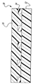
図1は、本発明の一実施例による光学的回折格子構造10の製造工程の断面図である。格子構造10は、MOCVD又はMBE等のエピタキシャル成長プロセスによって適合性半導体基板上で成長させた半導体層12を含む。この半導体層12を特定の光学的用途について所望の厚さまで成長させた後、ウェーハを結晶成長装置から取り出し、誘電体層、例えば二酸化珪素又は窒化珪素を半導体層12の上面に付着させる。ホログラフィー、電子ビーム書き込み露光技術等の適当な半導体パターン化プロセスによって誘電体層にパターンを付け、誘電体回折格子ストリップ14のパターンを形成する。化学的な又はプラズマを用いた任意の適当なエッチング等のエッチングプロセスを使用し、ストリップ14間の望ましからぬ誘電体部分をエッチングにより除去する。エッチングは、誘電体層の望ましからぬ誘電体部分が、図1に示すように、エッチングによってストリップ14間で層12を露呈するのに十分大きく除去されるように選択的に制御される。
The following discussion of a preferred embodiment of an optical semiconductor diffractometer and method of making the same is merely an example and is not intended to limit the invention or its use or use.
FIG. 1 is a sectional view of a manufacturing process of an optical diffraction grating structure 10 according to one embodiment of the present invention. The lattice structure 10 includes a semiconductor layer 12 grown on a compatible semiconductor substrate by an epitaxial growth process such as MOCVD or MBE. After growing the semiconductor layer 12 to a desired thickness for a particular optical application, the wafer is removed from the crystal growth apparatus and a dielectric layer, such as silicon dioxide or silicon nitride, is deposited on top of the semiconductor layer 12. The dielectric layer is patterned by a suitable semiconductor patterning process, such as holography, electron beam writing and exposure techniques, to form a pattern of dielectric grating strips. An unwanted dielectric portion between the strips 14 is etched away using an etching process, such as any suitable etching using chemical or plasma. The etching is selectively controlled such that unwanted dielectric portions of the dielectric layer are removed sufficiently large to expose the layer 12 between the strips 14, as shown in FIG.
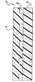
誘電体格子ストリップ14を層12上に形成した後、構造10を半導体成長装置に戻す。図2は、これに続いて行われる構造10の製造工程を示し、この工程では、エピタキシャル再成長プロセスによって第2半導体層16を層12上で成長させる。この層16は、ストリップ14間に露呈された層12とラチス適合しており、又はほぼラチス適合しており、層16を形成する。成長プロセスは、ストリップ14が完全に包囲されるまで続けられる。本説明の目的で、層12及び層16は同じ半導体で形成されているが、以下の議論から明らかになるように、成長プロセスに適合する限り、層16は層12と異なる半導体であってもよい。誘電体ストリップ14は、フィルタ等の光学装置用の回折格子を形成する。ストップ14の誘電体の屈折率は約1.5乃至2であり、そのため、ストリップ14と半導体材料との間の屈折率の差は、標準的なエピタキシャル成長半導体回折格子間の差よりも大きい。
After the dielectric grating strip 14 is formed on the layer 12, the structure 10 is returned to the semiconductor growth device. FIG. 2 shows a subsequent manufacturing step of the structure 10 in which a
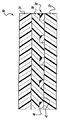
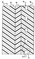
再成長工程後に誘電体ストリップ14を取り除いて図3に示すように空気チャンネル20を形成することによって、回折ストリップ14と半導体との間の屈折率の差を更に大きくできる。図4は、層16の製造後にストリップ14を選択的に取り除くための製造プロセスを示す、構造10の平面図である。最終的な光学装置用の使用可能な光学的領域を表す、光学装置領域22が構造10に形成される。光ビームは領域22をストリップ14に対して横方向に伝播する。通しエッチングチャンネル24及び26を構造10の上面を通して適当なマスキング及びエッチングプロセスによって、ストリップ14の端部が空気に露呈されるまで下方にパターンをなしてエッチングする。次いで、通しチャンネル24及び26に適当なエッチング剤を導入し、これによりストリップ14を選択的に除去し、空気チャンネル20を形成する。エッチングプロセスは、ストリップ14が全長に亘って除去されて空気チャンネル20が形成されたときに完了する。必要であれば、チャンネル開口部を閉鎖するのに十分な不活性化絶縁膜を通しチャンネル24及び26内に付着することによってチャンネル20をシールできる。
By removing the dielectric strip 14 after the regrowth step and forming the air channel 20 as shown in FIG. 3, the difference in the refractive index between the diffraction strip 14 and the semiconductor can be further increased. FIG. 4 is a plan view of the structure 10 showing a manufacturing process for selectively removing the strip 14 after the manufacture of the
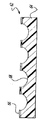
上文中に説明したプロセスで製造した構造10は、本発明の教示に従って様々な光学装置に使用できる。図5は、層12を表す下半導体クラッド層32及び上半導体クラッド層34を含む光学装置30の断面図である。装置30について、半導体層16は、屈折率がクラッド層32及び34よりも大きい半導体導波層36であり、この導波層36を伝播する光学的波動はこの層に閉じ込められる。この実施例では、回折格子層38が導波層36とクラッド層32との間の界面に形成される。回折格子層38は、ストリップ14を表す周期的に間隔が隔てられた誘電体ストリップ40、及びこれらのストリップ40間で成長した、導波層36の結晶再成長部分である半導体領域42を含む。ストリップ14をパターン化した後に構造10を結晶成長装置に再度導入したとき、導波層36は、クラッド層32を形成する材料と異なる適合性半導体材料として再成長する。次いで、クラッド層32と同じ材料のクラッド層34が導波層36上で成長する。従って、全ての層32、34、及び36は結晶成長プロセスに適合性である。上文中に論じたのと同様の方法でストリップ40を除去し、空気チャンネル20を形成できる。
Structure 10 manufactured by the process described above can be used in various optical devices in accordance with the teachings of the present invention. FIG. 5 is a cross-sectional view of the optical device 30 including the lower semiconductor cladding layer 32 and the upper semiconductor cladding layer 34 representing the layer 12. For the device 30, the
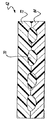
図6は、半導体領域54によって離間された空気チャンネル52によって形成された回折格子層50を持つ下クラッド層48を含む別の光学装置46の断面図である。この設計では、再成長層16はクラッド層48を形成する層12と同じ材料で形成されており、回折層50は埋設回折層である。空気チャンネル52を形成するためにストリップ14を除去する代わりに、ストリップ14を保持して上文中に論じた別の種類の光学装置を提供することができる。層16を再成長させて層48を形成した後、屈折率がクラッド層48よりも高い導波層56をクラッド48上で成長させ、上クラッド層58を導波層56上で成長させる。導波層56を伝播する波動は、当業者に理解されるように、光学的フィルタリングを行う目的でクラッド層48に進入し、回折層50と接触するモードを有する。クラッド層、回折格子層、及び導波層の任意の組み合わせを、適合性半導体層を互いの上でエピタキシャル成長させる上文中に論じた本発明の範疇で提供できる。
FIG. 6 is a cross-sectional view of another optical device 46 including a lower cladding layer 48 having a
図7乃至図10は、光学回折装置で使用されるべき、本発明の別の実施例による光学回折格子構造62の製造工程を示す断面図である。この実施例では、半導体層64は、適合性の半導体基板(図示せず)上で成長し、次いで誘電層を半導体層64に付着させ、これを適当なパターン化プロセスによってパターン化し且つエッチングし、誘電体ストリップ66を形成する。次いで、構造62をエッチング剤に露呈する。エッチング剤は、ストップ66間の層64の材料をエッチングにより除去するが、誘電体をエッチング除去せず、エッチング穴68を形成する。エッチングは、穴68の深さ及び形状を制御するように制御される。誘電体ストリップ66は、穴68内で犠牲半導体材料を選択的にエピタキシャル再成長させるためのマスクとして役立つ。次いで、構造62を成長装置に戻し、穴68内で犠牲半導体領域70を図示のように層64の上面とほぼ等しいレベルまで成長させる。領域70用の半導体は、領域70をエッチングによって選択的に除去できるが成長プロセスと適合できるように層64の材料とは異なる。
FIGS. 7 to 10 are cross-sectional views showing steps of manufacturing an optical diffraction grating structure 62 according to another embodiment of the present invention to be used in an optical diffraction apparatus. In this embodiment, semiconductor layer 64 is grown on a compatible semiconductor substrate (not shown), and then a dielectric layer is deposited on semiconductor layer 64, which is patterned and etched by a suitable patterning process, Form a
次いで、ストリップ66を、半導体材料に影響を及ぼさない適当なエッチングプロセスによって除去する。ストリップ66が除去されたとき、構造62を成長装置に戻し、別の半導体層72を領域70及び層64上で成長させ、領域70を図9に示すように包囲する。その後、エッチングチャンネル24及び26を使用する上文中に論じたエッチングプロセスによって犠牲領域70を除去し、回折格子層76を形成する空気チャンネル74を含む図10に示す構造を提供する。半導体層72は半導体層64と同じ半導体材料で形成されていてもよいし、上文中に説明したように、構造62が導波層とクラッド層との間に埋設回折層又は界面回折層を形成できるように別の半導体材料で形成されていてもよい。
ス ト リ ッ プ The
空気チャンネル20及び74を提供することによって、半導体材料と矛盾しない最大可能な結合係数を回折格子によって得ることができる。格子の歯高さ及び形状の正確性及び制御が従来の製造方法よりも大幅に改善される。ストリップ14間の又はチャンネル74間の空間的周期は、フィルタされる特定波長で決まる。ストリップ14の厚さは、設計者が光をどれ程強く回折しようとするのかで決まり、1000オングストローム程度である。上文中に論じた光学装置で使用できる半導体材料には、当業者に理解されるように、InP、InGaAs、GaAs、及び他の半導体材料が挙げられる。上文中に論じたプロセスによって、他の種類の光学装置についての平面的格子構造もまた形成できる。 By providing air channels 20 and 74, the maximum possible coupling coefficient consistent with the semiconductor material can be obtained with the diffraction grating. The accuracy and control of the tooth height and shape of the grid is greatly improved over conventional manufacturing methods. The spatial period between the strips 14 or between the channels 74 depends on the particular wavelength to be filtered. The thickness of the strip 14 depends on how strongly the designer attempts to diffract the light, and is on the order of 1000 angstroms. Semiconductor materials that can be used in the optical devices discussed above include InP, InGaAs, GaAs, and other semiconductor materials, as will be appreciated by those skilled in the art. By the processes discussed above, planar grating structures for other types of optical devices can also be formed.
以上は、本発明の単なる例示の実施例を論じ且つ説明したものである。特許請求の範囲に記載の本発明の精神及び範囲から逸脱することなく、様々な変形及び変更を行うことができるということは、当業者には、このような議論から及び添付図面及び特許請求の範囲から容易に理解されるであろう。 The foregoing discusses and describes merely exemplary embodiments of the present invention. It will be apparent to those skilled in the art, based on such discussion, that the drawings and claims may be varied, without departing from the spirit and scope of the invention, which is set forth in the following claims. It will be readily understood from the scope.
10 光学的回折格子構造
12 半導体層
14 誘電体回折格子ストリップ
16 第2半導体層
20 空気チャンネル
DESCRIPTION OF SYMBOLS 10 Optical diffraction grating structure 12 Semiconductor layer 14 Dielectric diffraction
Claims (21)
所定の屈折率を持つ半導体材料で形成される第1半導体層を半導体基板上で成長させる工程、
前記第1半導体層に誘電体層を付着する工程、
前記誘電体層にパターン化及びエッチングを施し、前記誘電体層に開口部を形成し、前記第1半導体層の選択的領域を露呈する工程、
前記誘電体層がマスクとして作用するように前記誘電体層の開口部を通して前記第1半導体層に穴をエッチングで形成する工程、及び
前記第1半導体層のエッチングで形成した穴で、前記第1半導体層の材料と適合性の半導体材料の結晶成長プロセスによって回折領域を成長する工程を有し、前記回折領域の材料の屈折率は、前記第1半導体層の屈折率と異なることを特徴とする方法。 In a method for manufacturing an optical diffraction device,
Growing a first semiconductor layer formed of a semiconductor material having a predetermined refractive index on a semiconductor substrate;
Attaching a dielectric layer to the first semiconductor layer;
Patterning and etching the dielectric layer, forming an opening in the dielectric layer, and exposing a selective region of the first semiconductor layer;
Etching a hole in the first semiconductor layer through an opening in the dielectric layer so that the dielectric layer acts as a mask; and forming the first hole in the hole formed by etching the first semiconductor layer. Growing a diffraction region by a crystal growth process of a semiconductor material compatible with the material of the semiconductor layer, wherein a refractive index of the material of the diffraction region is different from a refractive index of the first semiconductor layer. Method.
半導体基板上で第1半導体層を成長する工程、
前記第1半導体層に誘電体層を付着する工程、
前記誘電体層にパターン化及びエッチングを施し、前記誘電体層に開口部を形成し、前記第1半導体層の選択的領域を露呈し、前記開口部が実質的に平行なストリップを形成する工程、
前記第1半導体層に、前記誘電体層がマスクとして作用するように、前記誘電体層の前記ストリップの開口部を通して穴をエッチングで形成する工程、
前記第1半導体層にエッチングで形成した穴に、前記第1半導体層の材料とエピタキシャル成長について適合性であり且つ屈折率が前記第1半導体層の屈折率と異なる半導体材料で犠牲領域を成長する工程、
前記誘電体層を除去する工程、
第2半導体層を前記第1半導体層上で前記犠牲領域と接触してエピタキシャル成長プロセスによって成長する工程、
前記犠牲領域を露呈するように前記第2半導体層を通してアクセス通路をエッチングで形成する工程、及び
エッチングによって形成した前記アクセス通路を通して前記犠牲領域材料をエッチングで除去し、空気のチャンネルでできた回折格子を形成する工程を含むことを特徴とする方法。 In a method for manufacturing an optical diffraction device,
Growing a first semiconductor layer on a semiconductor substrate;
Attaching a dielectric layer to the first semiconductor layer;
Patterning and etching the dielectric layer to form openings in the dielectric layer, exposing selective areas of the first semiconductor layer, and forming strips with the openings being substantially parallel ,
Etching a hole in the first semiconductor layer through an opening in the strip of the dielectric layer such that the dielectric layer acts as a mask;
Growing a sacrificial region in a hole formed by etching in the first semiconductor layer with a semiconductor material compatible with the material of the first semiconductor layer for epitaxial growth and having a refractive index different from that of the first semiconductor layer. ,
Removing the dielectric layer,
Growing a second semiconductor layer on the first semiconductor layer by an epitaxial growth process in contact with the sacrificial region;
Etching an access passage through the second semiconductor layer to expose the sacrificial region; and etching the sacrificial region material through the access passage formed by etching to form a diffraction grating formed by an air channel. Forming a.
所定の屈折率を持つ半導体材料で形成される第1半導体層を半導体基板上で成長する工程、
前記第1半導体層に誘電体層を付着する工程、
前記誘電体層にパターン化及びエッチングを施し、前記誘電体層に開口部を形成し、前記第1半導体層の選択的領域を露呈し、前記誘電体材料でできた回折領域を形成する工程、及び
エピタキシャル成長プロセスによって第2半導体層を前記第1半導体層上に前記誘電体回折領域間で成長する工程を含むことを特徴とする方法。 In a method for manufacturing an optical diffraction device,
Growing a first semiconductor layer formed of a semiconductor material having a predetermined refractive index on a semiconductor substrate;
Attaching a dielectric layer to the first semiconductor layer;
Patterning and etching the dielectric layer, forming an opening in the dielectric layer, exposing selective areas of the first semiconductor layer, and forming a diffraction region made of the dielectric material; Growing a second semiconductor layer on the first semiconductor layer between the dielectric diffraction regions by an epitaxial growth process.
第1半導体層を半導体基板上で成長する工程、
前記第1半導体層の前記基板とは反対側に誘電体層を付着する工程、
前記誘電体層にパターン化及びエッチングを施し、前記誘電体層に開口部を形成し、前記第1半導体層の選択的領域を露呈し、間隔が隔てられた誘電体ストリップである誘電体回折領域を形成する工程、
第2半導体層を前記第1半導体層上の前記誘電体回折領域間でエピタキシャル成長プロセスによって、前記第2半導体層が前記誘電体回折領域を完全に包囲するように成長させる工程、
前記第2半導体層を通してアクセス通路をエッチングで形成し、前記誘電体回折領域を露呈する工程、及び
前記回折領域の材料をエッチングで除去し、空気でできた回折領域を形成する工程を含むことを特徴とする方法。 In a method for manufacturing an optical diffraction device,
Growing a first semiconductor layer on a semiconductor substrate;
Attaching a dielectric layer on the side of the first semiconductor layer opposite to the substrate;
Patterning and etching the dielectric layer, forming an opening in the dielectric layer, exposing selective areas of the first semiconductor layer, and a dielectric diffraction area that is a spaced dielectric strip; Forming a,
Growing a second semiconductor layer by an epitaxial growth process between the dielectric diffraction regions on the first semiconductor layer such that the second semiconductor layer completely surrounds the dielectric diffraction region;
Forming an access passage through the second semiconductor layer by etching to expose the dielectric diffraction region, and removing a material of the diffraction region by etching to form a diffraction region made of air. Features method.
Applications Claiming Priority (1)
| Application Number | Priority Date | Filing Date | Title |
|---|---|---|---|
| US10/210,799 US6649439B1 (en) | 2002-08-01 | 2002-08-01 | Semiconductor-air gap grating fabrication using a sacrificial layer process |
Publications (2)
| Publication Number | Publication Date |
|---|---|
| JP2004133407A true JP2004133407A (en) | 2004-04-30 |
| JP2004133407A5 JP2004133407A5 (en) | 2006-08-17 |
Family
ID=29420053
Family Applications (1)
| Application Number | Title | Priority Date | Filing Date |
|---|---|---|---|
| JP2003283547A Pending JP2004133407A (en) | 2002-08-01 | 2003-07-31 | Manufacture of semiconductor void grating using sacrificial layer process |
Country Status (4)
| Country | Link |
|---|---|
| US (2) | US6649439B1 (en) |
| EP (1) | EP1394911B1 (en) |
| JP (1) | JP2004133407A (en) |
| DE (1) | DE60319314T2 (en) |
Cited By (1)
| Publication number | Priority date | Publication date | Assignee | Title |
|---|---|---|---|---|
| JP2011215486A (en) * | 2010-04-01 | 2011-10-27 | Sumitomo Electric Ind Ltd | Mach-zehnder type optical modulator |
Families Citing this family (13)
| Publication number | Priority date | Publication date | Assignee | Title |
|---|---|---|---|---|
| US6944373B2 (en) * | 2002-08-01 | 2005-09-13 | Northrop Grumman Corporation | High index-step grating fabrication using a regrowth-over-dielectric process |
| US6649439B1 (en) * | 2002-08-01 | 2003-11-18 | Northrop Grumman Corporation | Semiconductor-air gap grating fabrication using a sacrificial layer process |
| US7116878B2 (en) * | 2003-04-24 | 2006-10-03 | Mesophotonics Ltd. | Optical waveguide structure |
| US7773836B2 (en) | 2005-12-14 | 2010-08-10 | Luxtera, Inc. | Integrated transceiver with lightpipe coupler |
| US7251386B1 (en) | 2004-01-14 | 2007-07-31 | Luxtera, Inc | Integrated photonic-electronic circuits and systems |
| KR100852110B1 (en) * | 2004-06-26 | 2008-08-13 | 삼성에스디아이 주식회사 | An organic electroluminescent display device and method for preparing the same |
| SG139547A1 (en) * | 2004-08-04 | 2008-02-29 | Agency Science Tech & Res | Distributed feedback and distributed bragg reflector semiconductor lasers |
| DE102006036831B9 (en) * | 2006-08-07 | 2016-04-14 | Friedrich-Schiller-Universität Jena | Closed, binary transmission grids |
| US20090229651A1 (en) * | 2008-03-14 | 2009-09-17 | Fay Jr Theodore Denis | Solar energy production system |
| DE102008054217A1 (en) * | 2008-10-31 | 2010-05-06 | Osram Opto Semiconductors Gmbh | Optoelectronic semiconductor chip and method for producing an optoelectronic semiconductor chip |
| US20110068279A1 (en) * | 2009-08-11 | 2011-03-24 | Fay Jr Theodore Denis | Ultra dark field microscope |
| CN114731025A (en) * | 2020-02-29 | 2022-07-08 | 华为技术有限公司 | DFB laser |
| PL439368A1 (en) | 2021-10-30 | 2023-05-02 | Instytut Wysokich Ciśnień Polskiej Akademii Nauk Unipress | Method for generating an area with a regularly varying refractive index in a selected layer of a layered semiconductor structure |
Family Cites Families (13)
| Publication number | Priority date | Publication date | Assignee | Title |
|---|---|---|---|---|
| JPH0231488A (en) * | 1988-07-20 | 1990-02-01 | Mitsubishi Electric Corp | Semiconductor laser device and its manufacture |
| IT1245541B (en) * | 1991-05-13 | 1994-09-29 | Cselt Centro Studi Lab Telecom | SEMICONDUCTOR LASER WITH DISTRIBUTED REACTION AND PAIR OF GAIN, AND PROCEDURE FOR ITS MANUFACTURE |
| US5955749A (en) * | 1996-12-02 | 1999-09-21 | Massachusetts Institute Of Technology | Light emitting device utilizing a periodic dielectric structure |
| FR2765347B1 (en) * | 1997-06-26 | 1999-09-24 | Alsthom Cge Alcatel | SEMICONDUCTOR BRAGG REFLECTOR AND MANUFACTURING METHOD |
| US6358854B1 (en) * | 1999-04-21 | 2002-03-19 | Sandia Corporation | Method to fabricate layered material compositions |
| US6468823B1 (en) * | 1999-09-30 | 2002-10-22 | California Institute Of Technology | Fabrication of optical devices based on two dimensional photonic crystal structures and apparatus made thereby |
| EP1094345A1 (en) * | 1999-10-19 | 2001-04-25 | BRITISH TELECOMMUNICATIONS public limited company | Method of making a photonic band gap structure |
| EP1265326B1 (en) * | 2000-03-13 | 2009-05-13 | Sharp Kabushiki Kaisha | Gain-coupled distributed feedback semiconductor laser device and production method therefor |
| JP2001281473A (en) * | 2000-03-28 | 2001-10-10 | Toshiba Corp | Photonics crystal and method for manufacturing the same, optical module as well as optical system |
| US6365428B1 (en) * | 2000-06-15 | 2002-04-02 | Sandia Corporation | Embedded high-contrast distributed grating structures |
| US6560006B2 (en) * | 2001-04-30 | 2003-05-06 | Agilent Technologies, Inc. | Two-dimensional photonic crystal slab waveguide |
| US6649439B1 (en) * | 2002-08-01 | 2003-11-18 | Northrop Grumman Corporation | Semiconductor-air gap grating fabrication using a sacrificial layer process |
| US6944373B2 (en) * | 2002-08-01 | 2005-09-13 | Northrop Grumman Corporation | High index-step grating fabrication using a regrowth-over-dielectric process |
-
2002
- 2002-08-01 US US10/210,799 patent/US6649439B1/en not_active Expired - Fee Related
-
2003
- 2003-07-29 DE DE60319314T patent/DE60319314T2/en not_active Expired - Fee Related
- 2003-07-29 EP EP03016613A patent/EP1394911B1/en not_active Expired - Lifetime
- 2003-07-31 JP JP2003283547A patent/JP2004133407A/en active Pending
- 2003-09-03 US US10/654,315 patent/US6893891B2/en not_active Expired - Fee Related
Cited By (2)
| Publication number | Priority date | Publication date | Assignee | Title |
|---|---|---|---|---|
| JP2011215486A (en) * | 2010-04-01 | 2011-10-27 | Sumitomo Electric Ind Ltd | Mach-zehnder type optical modulator |
| US9146442B2 (en) | 2010-04-01 | 2015-09-29 | Sumitomo Electric Industries, Ltd. | Mach-Zehnder interferometer type optical modulator |
Also Published As
| Publication number | Publication date |
|---|---|
| EP1394911B1 (en) | 2008-02-27 |
| DE60319314D1 (en) | 2008-04-10 |
| DE60319314T2 (en) | 2009-02-26 |
| US20040082152A1 (en) | 2004-04-29 |
| EP1394911A2 (en) | 2004-03-03 |
| US6893891B2 (en) | 2005-05-17 |
| EP1394911A3 (en) | 2005-06-08 |
| US6649439B1 (en) | 2003-11-18 |
Similar Documents
| Publication | Publication Date | Title |
|---|---|---|
| EP0604407B1 (en) | Photonic-integrated-circuit fabrication process | |
| US8290014B2 (en) | Active photonic device | |
| US4420873A (en) | Optical guided wave devices employing semiconductor-insulator structures | |
| US6292503B1 (en) | Ridge type semiconductor laser of laterally-coupled distributed feedback and method of manufacturing the same | |
| JP2004133407A (en) | Manufacture of semiconductor void grating using sacrificial layer process | |
| WO2009120353A2 (en) | Semiconductor buried grating fabrication method | |
| KR20060131683A (en) | Buried heterostructure device having integrated waveguide grating fabricated by single step mocvd | |
| JP2004133408A (en) | Manufacture of high refractive index-step grating using regrowth-over-dielectric process | |
| KR20000006219A (en) | Process for fabricating an optical waveguide | |
| JPH01214089A (en) | Method of forming diffraction lattice in semiconductor material and photoelectric device with the diffraction lattice manufactured by the method | |
| JPH0685458B2 (en) | Method of manufacturing a laser having a mirror facet | |
| CN115149399A (en) | Grating laser and preparation method | |
| JP2000077770A (en) | Semiconductor laser and formation method of there | |
| JP2634687B2 (en) | Tapered semiconductor waveguide and method of forming the same | |
| JP2000193813A (en) | Diffraction grating formation method, diffraction grating and optical semiconductor element | |
| JPH09191151A (en) | Manufacture of distributed feedback laser having spatial change in diffraction grating coupling along length of laser cavity | |
| CN112993760B (en) | Semiconductor manufacturing method | |
| US20230261435A1 (en) | Optoelectronic device and method of preparation thereof | |
| JPH04229679A (en) | Semiconductor laser | |
| JP2682414B2 (en) | Method for forming semiconductor quantum fine structure | |
| JP2892122B2 (en) | Manufacturing method of semiconductor laser | |
| CN116953864A (en) | Silicon optical chip suitable for direct coupling of laser and waveguide and manufacturing method thereof | |
| JPS61212803A (en) | Manufacture of diffraction grating | |
| KR19980050572A (en) | Method for manufacturing diffraction grating coupler | |
| JPH0590705A (en) | Optical semiconductor device |
Legal Events
| Date | Code | Title | Description |
|---|---|---|---|
| A521 | Request for written amendment filed |
Free format text: JAPANESE INTERMEDIATE CODE: A523 Effective date: 20060629 |
|
| A621 | Written request for application examination |
Free format text: JAPANESE INTERMEDIATE CODE: A621 Effective date: 20060629 |
|
| A131 | Notification of reasons for refusal |
Free format text: JAPANESE INTERMEDIATE CODE: A131 Effective date: 20090331 |
|
| A02 | Decision of refusal |
Free format text: JAPANESE INTERMEDIATE CODE: A02 Effective date: 20091019 |