JP2004128233A - Suction nozzle and die bonding equipment - Google Patents
Suction nozzle and die bonding equipment Download PDFInfo
- Publication number
- JP2004128233A JP2004128233A JP2002290605A JP2002290605A JP2004128233A JP 2004128233 A JP2004128233 A JP 2004128233A JP 2002290605 A JP2002290605 A JP 2002290605A JP 2002290605 A JP2002290605 A JP 2002290605A JP 2004128233 A JP2004128233 A JP 2004128233A
- Authority
- JP
- Japan
- Prior art keywords
- suction nozzle
- nozzle
- plate
- suction
- heat insulating
- Prior art date
- Legal status (The legal status is an assumption and is not a legal conclusion. Google has not performed a legal analysis and makes no representation as to the accuracy of the status listed.)
- Granted
Links
Images


Landscapes
- Die Bonding (AREA)
Abstract
Description
【0001】
【発明の属する技術分野】
本発明は、半導体素子、特に高精度位置決めが必要とされる光半導体素子を基板上の所定の位置に位置決めし、加熱しながらその位置に固着させるダイボンディング装置およびその吸着ノズルに関する。
【0002】
【従来の技術】
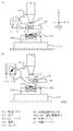
従来のダイボンディング装置においては、吸着ノズルで半導体素子を吸着し、次いで、基板表面の所望の位置に半導体素子を押し付けた後、基板を載置している加熱ステージを用いて基板上の半田を溶解して、半導体素子を基板上に固着させている(例えば、特許文献1参照。)。図5を用いて、この従来例のダイボンディング装置の動作手順を説明する。まず、図5(a)に示すように、可動テーブル152を用いて、吸着ノズル110に吸着された素子120の下方に基板130を配置させる。次に、素子120と基板130との間に位置認識用光学系140を進入させ、上側の固体撮像素子140bを素子120の下面に形成されている2つのマーク121の真下に位置させて、両マーク121の位置を認識させる。次いで、図1(b)に示すように、位置認識用光学系140を後退させて下側の固体撮像素子140cを基板130の上面に形成されている2つのマーク131の真上に位置させ、両マーク131を認識させる。これら2つの認識から、素子120と基板130との相対的な位置関係が算出され、所望の位置関係からどれだけずれているかが算定される。続いて、このずれを相殺するように可動テーブル152を用いて基板130を移動させる。そして再度位置認識用光学系140を用いて、前記の場合と同様に素子120と基板130との相対的な位置関係を確認する。この操作をずれが零になるまで繰り返し、零になった時点で位置認識用光学系140を待避させ、吸着ノズル110を下げて、それに保持されている素子120をはんだ132および基板130に対して押し付け、加熱ステージ150ではんだ132を溶解し、素子120を基板130にボンディングさせる。
【0003】
しかしながら、上述の従来技術においては、素子120と基板130とをそれぞれ異なる固体撮像素子140b、140cによって認識することに伴う測定の軸ずれ、位置認識用光学系140の移動の際の装置のあそび等による測定誤差、固体撮像素子による複数回の素子120および基板130の認識の必要性などの問題が生じる。
【0004】
そこで、これらの問題点を解決できるダイボンディング装置が提案されている(例えば、特許文献2参照。)。図6は、この従来例のダイボンディング装置の吸着ノズルの正面断面図である。図6に示すように、この従来の吸着ノズルは、素子220を吸着保持するノズルチップ201と、ノズルチップ201を支持する光透過性支持部材211と、光透過性支持部材211との間に吸引室207を形成する光透過性カバー部材212と、光透過性支持部材211および光透過性カバー部材212を保持する筒状のコレット204とからなる。また、ノズルチップ201の吸着孔206は、吸引室207、吸引室口207aにつながっており、吸引室口207aに吸引ポンプ(図示せず)を接続することによって、ノズルチップ201の吸着孔206に素子220を吸着できるようになっている。この従来の吸着ノズルを有するボンディング装置を用いて素子を基板に固着させるには、最初に、コレット204の上部にコレット204と中心軸が同軸に配置された位置認識用光学系(図示せず)を用いて素子220の位置認識を行い、吸着ノズルを位置決めして素子220を吸着する。次に、素子220の下方に基板230を移動させ、位置認識用光学系を用いて基板230の所望の素子固着位置を認識した後、吸着ノズルを位置決めして素子220を銀ペーストが塗布された素子固着位置に下ろす。最後に、基板230をボンディングステージ260から取り出し、別工程において電気オーブン等を用いて銀ペーストを加熱硬化させて、素子220を最終的に基板230に固着させる。
【0005】
【特許文献1】
特開平06−216170号公報 (第3頁、図1)
【特許文献2】
特開2000−299501号公報 (第4−6頁、図3、図4、図5、図9、図11、図15)
【0006】
【発明が解決しようとする課題】
しかしながら、特開平06−216170号公報に開示のダイボンディング装置は、基板が載置された加熱ステージだけを用いて基板を加熱し、吸着ノズル側に加熱手段を持たないため、上述の問題点以外にも、基板への固着前に素子を予熱することができず、ダイボンディングに時間がかかるという問題も有している。また、複数の素子を一枚の基板に固着させる場合には、後から載せる素子を固着させるときにも基板全体を加熱しなければならず、先に固着させた素子の固着部のはんだが溶けて位置ずれを起こすという問題もある。また、耐熱性の異なる複数の素子を搭載させる場合には、搭載順序に制約が出るという問題もある。
【0007】
一方、特開2000−299501号公報に開示のダイボンディング装置においては、素子を載せた基板をボンディングステージから取り出した後、銀ペーストを最終的に加熱硬化させるまでの間に、素子の位置ずれが起こる危険性が存在する。また、このダイボンディング装置において、高精度に位置認識を行うためには光学系の倍率を高くする必要があり、高倍率の対物レンズが使用されることになるが、対物レンズの倍率が高くなるほど、レンズ先端と合焦位置までの作動距離が短くなる。たとえば、倍率20倍の対物レンズの場合、長作動距離対応のものでも、その作動距離は20mm程度である。このため、この対物レンズの直下に、対物レンズと同軸に配置される吸着ノズルは、ノズルの上下作動範囲を除くと、十数mmの高さに収められる必要がある。したがって、位置認識用光学系の視野を大きく遮ることなく、吸着ノズルに加熱機構を付加することは困難であるという問題があった。
【0008】
本発明は、上記課題に鑑みてなされたものであって、その目的は、位置認識用光学系の視野を大きく遮ることなく加熱手段を組み込んだ吸着ノズルおよびその吸着ノズルを用いたダイボンディング装置を提供することである。
【0009】
【課題を解決するための手段】
上記目的を達成するため、本発明によれば、被吸着物を吸着する吸着ノズルであって、前記吸着された被吸着物を固定する面を有するノズルチップと、前記ノズルチップを下面に保持する板状のヒータプレートとを有することを特徴とする吸着ノズル、が提供される。
そして、より好ましくは、ノズルチップは、その上面から下面に向けて幅が狭くなっており、板状のヒータプレートの上に、ヒータプレートを下面に保持する板状の断熱プレートと、該断熱プレートを下面に保持する板状の保持部を有するコレットとが形成されている。
【0010】
また、上記目的を達成するため、本発明によれば、前記吸着ノズルと、前記吸着ノズルに吸着された被吸着物が固着される基板またはリードフレームの位置を認識するための光学系とを有するダイボンディング装置であって、前記光学系が、前記吸着ノズルの上方に、または、前記吸着ノズルのコレットにその一部を挿入して、前記光学系の光軸を通る、前記コレットの保持部の長手方向に直交する平面において、前記コレットの保持部と断熱プレートとヒータプレートとノズルチップとを光路内に内包するように配置されていることを特徴とするダイボンディング装置、が提供される。
【0011】
〔効果〕
本発明に係る吸着ノズルは、吸着された被吸着物を固定する面を有するノズルチップと、ノズルチップを下面に保持する板状のヒータプレートよりなるノズルチップの加熱手段とを有するものである。これによって、短時間での基板への素子の固着および複数の素子の位置精度の高い固着が可能になる。
【0012】
本発明に係るダイボンディング装置は、位置認識用光学系の光路内に、吸着ノズルのコレットを除く大部分を内包するように構成されるものである。これによって、素子吸着位置における素子の高精度の位置認識、および素子固着位置における基板の高精度の位置認識が可能である。請求項2に記載の吸着ノズルは、このようなダイボンディング装置の実現を可能にする。
【0013】
請求項3に記載の吸着ノズルは、そのノズルチップが上面から下面に向けて幅が狭くなるものであり、これによって、吸着される素子の均一かつ効率的な温度上昇が可能になる。
請求項4に記載の吸着ノズルは、そのヒータプレートが自己発熱体で形成されるものであり、これによって、薄いヒータプレートが挿入された吸着ノズルの実現が可能になる。
請求項6に記載の吸着ノズルは、吸着ノズルを形成する各部を貫通するように吸引路が形成されるものであり、これによって、余分な吸引路の形成が不用になり、小型・薄型の吸着ノズルの実現が可能にする。
請求項7に記載の吸着ノズルは、ノズルチップとヒータプレートと断熱プレートとに連結して位置ずれ防止ピンが設けられるものであり、これによって、ノズルチップ、ヒータプレート、および、断熱プレートの各部材の熱膨張率の差に起因して生じるノズルチップ、ヒータプレート、断熱プレートの変形や位置ずれが抑えられ、ノズルチップの下面に吸引された素子の位置決めが高精度に行なわれる。
【0014】
【発明の実施の形態】
次に、本発明の実施の形態について、図面を参照して説明する。
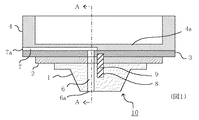
図1は、本発明に係る吸着ノズルの正面断面図である。図2は、図1のA−A線に沿う断面図である。図3は、図1の底面図である。全図を通じて、同一部分には同一符号が付されている。本発明に係る吸着ノズル10は、ノズルチップ1と、ノズルチップ1を下面に保持する細長い板状のヒータプレート2と、ヒータプレート2を下面に保持する細長い板状の断熱プレート3と、断熱プレート3を下面に保持する細長い板状の保持部4aを有するコレット4と、を有している。ノズルチップ1とヒータプレート2と断熱プレート3とには、それらを貫通し、ノズルチップ1の先端平面に吸着孔口6aを有する吸着孔6が形成されている。ノズルチップ1とヒータプレート2と断熱プレート3とには、また、それらを連結する位置ずれ防止ピン9が嵌合された位置ずれ防止穴8が形成されている。コレット4の保持部4aには、吸着孔6の断熱プレート3側の口から、紙面左端の吸着溝口7aに達する吸着溝7が形成されている。ノズルチップ1は、ヒータプレート2への取り付け部である上面から、吸着孔口6aが形成されているノズル先端部に向けて長さおよび幅が短くなる角錐台形状をなしている。コレット4の底面には、保持部4aを除いて、窓(開口)5a、5bが開いている。窓5a、5bには、ガラス、あるいは、アクリルなどの樹脂が嵌め込まれていてもよい。
【0015】
このような構成を有する本発明に係る吸着ノズルが、ダイボンディング装置本体に、上下可動に取り付けられている。吸着溝口7aに吸引ポンプ(図示せず)を接続して吸引することによって、ノズルチップ1の底面に接して、あるいは、その近傍に置かれた半導体素子等をノズルチップ1の吸着孔口6aに吸着し、その底面に固定することができる。
【0016】
ヒータプレート2に例えば通電によって自己発熱するSiCセラミックス等の材料(自己発熱体)を用いることによって、ヒータプレート2を細く、かつ、薄い板状に容易に形成することができる。そして、細い板状のヒータプレート2の長手方向の両端に形成した電極部(図示せず)を介して通電することによって、ノズルチップ1の底面に固定された半導体素子等への加熱を行うことができる。
【0017】
ノズルチップ1に電気絶縁体で、かつ、熱を良く伝えるAlNセラミックス等の材料を用い、ヒータプレート2の電極部が形成された両端部を除き、ヒータプレート2の下面とノズルチップ1の上面とが広く接触する構造をとることによって、ノズルチップ1の先端に効率良く熱が伝達される。また、ノズルチップ1が、ノズルチップ先端に向けて順次細くなる角錐台形状となっているため、ヒータプレート2からの熱によるノズルチップ先端の温度上昇が大きくなり、かつ、下面全体に渡って温度が均一になる。一般に個々の光素子は小さいが、複数個連結してバー状の光素子アレイとされることが多い。このような細長いバー状の素子アレイに対しても、ノズルチップを角錐台形状で、そのノズルチップの先端平面部の形状を同じように細長くすることによって、均一かつ効率的な温度上昇を行うことができる。
【0018】
断熱プレート3には電気絶縁体で、かつ、熱の伝導度の悪いアルミナセラミックス等の材料を用いることによって、ヒータプレート2からコレット4への熱の伝導が抑えられる。また、コレット4に形成された溝7は、コレット4の保持部4aと断熱プレート3との接触面積を少なくするため、断熱プレート3からコレット4への熱の伝導を抑える効果も有する。
【0019】
位置ずれ防止穴8は、吸着ノズル10の中心軸に重なって形成されることが望ましい。その場合には、ヒータプレート2による加熱冷却時に、ノズルチップ1、ヒータプレート2、および、断熱プレート3の各部材の熱膨張率の差に起因して生じるノズルチップ1、ヒータプレート2、断熱プレート3の変形や位置ずれを最小限に抑えることができ、ノズルチップ1の下面に吸引された素子の位置決めを高精度に行うことが可能である。しかしながら、吸着孔6が吸着ノズル10の中心軸近傍に形成されている場合には、位置ずれ防止穴8を中心軸からずらして配置することも可能である。その場合でも、位置ずれ防止穴8は、できるだけ中心軸の近くに形成されることが望ましい。
【0020】
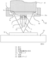
次に、図4を用いて、本発明に係る吸着ノズル全体の動作を、より詳細に説明する。図4は、本発明に係る吸着ノズルの動作を説明するための断面図である。図4において、図2の部分と同等の部分には等しい参照符号を付し重複する説明を適宜省略する。図4は、ノズルチップ先端に、素子20が吸着・保持された状態を示している。また、吸着ノズル10の直上に配置された位置認識用光学系40の先端部分がコレット4の内部に、それら両方の中心軸を同軸にして挿入されている。位置認識用光学系40の先端には対物レンズ40aが設けられており、位置認識用光学系40によって、基板30上の位置を確認できる構成になっている。このとき、対物レンズ40の直下に、コレット4の保持部4aと断熱プレート3とヒータプレート2とノズルチップ1と素子20とがあり、対物レンズ40aの視野の一部が遮られることになる。しかしながら、ノズルチップ1は、その先端に向かって長さおよび幅が漸次短くなる細長い角錐台形状をなしており、素子20もノズルチップ1の下面内に吸着されているので、少なくとも位置認識用光学系40の光軸の近傍を通り、コレットの保持部4aの長手方向に直交する平面においては、コレット4の窓5a、5bを通して、コレット4の保持部4aと断熱プレート3とヒータプレート2と角錐台形状のノズルチップ1を内部に含んだ光路41が確保されており、加熱ステージ50上に載置された基板30上の位置の認識が可能である。同様に、ノズルチップ先端に素子20を吸着させるときも、素子載置台上に置かれた素子20の位置認識が可能となることは明らかである。
【0021】
したがって、図4に示された状態で吸着ノズルがボンディング装置に組み込まれていると、素子吸着時に素子の位置認識/位置決めを行い、その位置で吸着ノズルを上下させて素子を吸着させることができる。また、基板への素子の固着時に基板の位置認識/位置決めを行い、その位置で吸着ノズルを上下して固着させることができる。基板には、予め、所定の位置に共晶合金、はんだ、あるいは、銀ペースト等が塗布されている。素子の吸着時および固着時に吸着ノズルはわずかに上下動するだけなので、位置精度の高い固着が可能となる。また、吸着ノズルに加熱手段を設けてあるので、基板への固着前に素子の予備加熱を行うことが可能であり、短時間で良好な固着を行うことが可能となる。一枚の基板に複数の素子を固着させる場合には、基板を加熱せずに吸着ノズルの加熱手段だけで素子を加熱することができるので、2番目以降に素子を固着させる際に、先に高精度に位置決めして固着させた素子のはんだ等が溶けて位置ずれが起こるということがない。あるいは、一枚の基板に複数の素子を固着させる場合、2番目以降に素子を固着させる際に、先に固着させた素子の加熱温度以下に基板を加熱し、必要に応じて吸着ノズルの加熱手段を用いて素子をさらに加熱することによって、基板上に素子を固着させてもよい。さらに、基板に既に耐熱温度の低い素子が搭載されている場合にも、ノズルチップ先端に吸着されている素子を吸着ノズルの加熱手段のみで加熱して基板に固着させることが可能である。したがって、耐熱温度の低い素子を先に基板に固着させておくことも可能であり、基板上への素子の搭載順序の制約もない。
【0022】
上記のように、本発明に係るボンディング装置は、素子吸着位置における素子の高精度の位置認識、および素子固着位置における基板の高精度の位置認識が可能で、その場で素子の吸着、固着が可能なため、μmオーダーの高精度の位置決めが必要な光半導体素子等の組立に適用可能である。
【0023】
以上、本発明をその好適な実施の形態に基づいて説明したが、本発明の吸着ノズルおよびそれを用いたダイボンディング装置は、上述した実施の形態のみに制限されるものではなく、本願発明の要旨を変更しない範囲で種々の変化を施した吸着ノズルおよびそれを用いたダイボンディング装置も、本発明の範囲に含まれる。例えば、ヒータプレートは、自己発熱型の材料に限られることはなく、微細な電熱線を絶縁材に埋め込んだものでもよく、位置認識用光学系の光路内に納まる程度に薄くかつ細い形状のヒータであればどのようなものであっても用い得る。その際、ノズルチップには、必ずしも電気絶縁材でない金属材料等が使用されてもよい。また、ノズルチップとヒータプレートと断熱プレートとコレットの保持部とは、それらの全領域において幅細く形成される必要はなく、位置認識用光学系が基板上の位置を確認できる限り、とりわけ位置認識用光学系の光路外において、どのような形状に形成されてもよい。また、コレットの保持部の吸着溝は、必ずしも吸着孔の断熱プレート側の口から直線状に設けられる必要はなく、吸着孔の断熱プレート側の口に連絡し、外部に配置された吸引ポンプ等の吸引手段によってノズルチップの吸着孔口に素子を吸着できる配管通路を構成する限り、どのような形状に形成されてもよい。さらに、この吸着溝は、コレットの保持部ではなく、断熱プレートに、あるいは、コレットの保持部と断熱プレートとにまたがって、設けられてもよい。また、とりわけ基板を載置する加熱ステージを主加熱源とし、ヒータプレートを補助加熱源として使用する場合のようにヒータプレートの温度をあまり上げないときには、熱膨張の差の影響が少ないため、位置ずれ防止穴の形成、および、位置ずれ防止ピンの設置が省略されてもよい。また、位置認識用光学系の中心軸(光軸)と吸着ノズルの中心軸とは必ずしも一致する必要はなく、軸ずれ量がわかっていればよい。また、素子が固着される基板は、リードフレームであってもよい。さらに、ノズルチップ先端の温度をコントロールするために、ノズルチップの長手方向の端部や、ヒータプレートとノズルチップとの間などの位置認識用光学系の視野を遮らない位置に、熱電対等の温度センサが設置されてもよい。
【0024】
【発明の効果】
以上説明したように、本発明に係る吸着ノズルは、吸着された被吸着物を固定する面を有するノズルチップと、ノズルチップを加熱する加熱手段とを有するものであるから、短時間での基板への素子の固着および複数の素子の位置精度の高い固着が可能になる。
【0025】
また、本発明に係るダイボンディング装置は、位置認識用光学系の光路内に、吸着ノズルのコレットを除く大部分を内包するように構成されるものであるから、素子吸着位置における素子の高精度の位置認識、および素子固着位置における基板の高精度の位置認識が可能である。
【図面の簡単な説明】
【図1】本発明に係る吸着ノズルの正面断面図。
【図2】図1のA−A線に沿う断面図。
【図3】図1の底面図。
【図4】本発明に係る吸着ノズルの動作を説明するための断面図。
【図5】従来例のダイボンディング装置の主要部の正面図。
【図6】従来例の吸着ノズルの断面図。
【符号の説明】
1 ノズルチップ
2 ヒータプレート
3 断熱プレート
4 コレット
4a 保持部
5a、5b 窓
6 吸着孔
6a 吸着孔口
7 吸着溝
7a 吸着溝口
8 位置ずれ防止穴
9 位置ずれ防止ピン
10 吸着ノズル
20 素子
30 基板
40 位置認識用光学系
40a 対物レンズ
41 光路
50 加熱ステージ
110 吸着ノズル
120 素子
121、131 マーク
130 基板
132 はんだ
140 位置認識用光学系
140b、140c 固体撮像素子
150 加熱ステージ
152 可動テーブル
201 ノズルチップ
206 吸着孔
207 吸引室
207a 吸引室口
211 光透過性支持部材
212 光透過性カバー部材
220 素子
230 基板
260 ボンディングステージ[0001]
TECHNICAL FIELD OF THE INVENTION
The present invention relates to a die bonding apparatus and a suction nozzle for positioning a semiconductor element, particularly an optical semiconductor element requiring high-precision positioning, at a predetermined position on a substrate and fixing the semiconductor element at that position while heating.
[0002]
[Prior art]
In a conventional die bonding apparatus, a semiconductor element is suctioned by a suction nozzle, and then the semiconductor element is pressed to a desired position on the substrate surface, and then the solder on the substrate is heated using a heating stage on which the substrate is mounted. By melting, the semiconductor element is fixed on the substrate (for example, see Patent Document 1). The operation procedure of this conventional die bonding apparatus will be described with reference to FIG. First, as shown in FIG. 5A, the
[0003]
However, in the above-described related art, the axis of measurement caused by recognizing the
[0004]
Therefore, a die bonding apparatus capable of solving these problems has been proposed (for example, see Patent Document 2). FIG. 6 is a front sectional view of a suction nozzle of the conventional die bonding apparatus. As shown in FIG. 6, this conventional suction nozzle includes a
[0005]
[Patent Document 1]
JP-A-06-216170 (page 3, FIG. 1)
[Patent Document 2]
Japanese Patent Application Laid-Open No. 2000-299501 (Pages 4-6, FIGS. 3, 4, 5, 9, 11, and 15)
[0006]
[Problems to be solved by the invention]
However, the die bonding apparatus disclosed in Japanese Patent Application Laid-Open No. 06-216170 heats the substrate using only the heating stage on which the substrate is mounted, and has no heating means on the suction nozzle side. In addition, there is also a problem that the element cannot be preheated before being fixed to the substrate, and it takes time for die bonding. When a plurality of elements are fixed to a single substrate, the entire substrate must be heated even when the elements to be mounted later are fixed. There is also a problem that misalignment occurs. In addition, when a plurality of elements having different heat resistances are mounted, there is a problem that the mounting order is restricted.
[0007]
On the other hand, in the die bonding apparatus disclosed in Japanese Patent Application Laid-Open No. 2000-299501, after the substrate on which the element is mounted is taken out from the bonding stage, the position of the element is displaced until the silver paste is finally heated and cured. There is a risk of happening. Further, in this die bonding apparatus, it is necessary to increase the magnification of the optical system in order to perform position recognition with high accuracy, and a high-magnification objective lens is used. The working distance between the lens tip and the in-focus position is shortened. For example, in the case of an objective lens having a magnification of 20 times, the working distance is about 20 mm even if the objective lens corresponds to a long working distance. For this reason, the suction nozzle, which is disposed directly below the objective lens and coaxially with the objective lens, needs to be housed at a height of more than ten mm, excluding the vertical operation range of the nozzle. Therefore, there is a problem that it is difficult to add a heating mechanism to the suction nozzle without largely obstructing the field of view of the position recognition optical system.
[0008]
The present invention has been made in view of the above problems, and has as its object to provide a suction nozzle incorporating a heating means without largely obstructing the field of view of a position recognition optical system, and a die bonding apparatus using the suction nozzle. To provide.
[0009]
[Means for Solving the Problems]
In order to achieve the above object, according to the present invention, there is provided a suction nozzle for adsorbing an object to be adsorbed, the nozzle tip having a surface for fixing the object to be adsorbed, and the nozzle chip being held on a lower surface. A suction nozzle having a plate-like heater plate is provided.
More preferably, the nozzle tip is narrower in width from the upper surface to the lower surface, and a plate-shaped heat insulating plate for holding the heater plate on the lower surface, on the plate-shaped heater plate, And a collet having a plate-like holding portion for holding the plate on the lower surface.
[0010]
In order to achieve the above object, according to the present invention, there is provided the suction nozzle, and an optical system for recognizing a position of a substrate or a lead frame to which an object to be suctioned is fixed by the suction nozzle. A die bonding apparatus, wherein the optical system is provided above the suction nozzle or by inserting a part of the collet into the collet of the suction nozzle and passing through the optical axis of the optical system. A die bonding apparatus is provided in which a holding portion of the collet, a heat insulating plate, a heater plate, and a nozzle chip are disposed in a light path on a plane orthogonal to the longitudinal direction.
[0011]
〔effect〕
The suction nozzle according to the present invention includes a nozzle chip having a surface for fixing the suctioned object to be sucked, and a nozzle chip heating means including a plate-like heater plate for holding the nozzle chip on a lower surface. Thus, it is possible to fix the element to the substrate in a short time and to fix the plurality of elements with high positional accuracy.
[0012]
The die bonding apparatus according to the present invention is configured to include most of the suction nozzle except for the collet in the optical path of the position recognition optical system. This enables highly accurate position recognition of the element at the element suction position and high accuracy position recognition of the substrate at the element fixed position. The suction nozzle according to the second aspect makes it possible to realize such a die bonding apparatus.
[0013]
In the suction nozzle according to the third aspect, the width of the nozzle tip becomes narrower from the upper surface to the lower surface, whereby the temperature of the element to be sucked can be increased uniformly and efficiently.
In the suction nozzle according to the fourth aspect, the heater plate is formed of a self-heating element, thereby realizing a suction nozzle in which a thin heater plate is inserted.
In the suction nozzle according to the sixth aspect, the suction path is formed so as to penetrate the respective parts forming the suction nozzle, so that the formation of an extra suction path is unnecessary and the suction nozzle is small and thin. A nozzle can be realized.
The suction nozzle according to
[0014]
BEST MODE FOR CARRYING OUT THE INVENTION
Next, embodiments of the present invention will be described with reference to the drawings.
FIG. 1 is a front sectional view of a suction nozzle according to the present invention. FIG. 2 is a sectional view taken along line AA of FIG. FIG. 3 is a bottom view of FIG. Throughout the drawings, the same portions are denoted by the same reference numerals. The
[0015]
The suction nozzle according to the present invention having such a configuration is attached to the die bonding apparatus main body so as to be vertically movable. By connecting a suction pump (not shown) to the suction groove orifice 7a and performing suction, a semiconductor element or the like placed in contact with or near the bottom surface of the
[0016]
By using a material (self-heating element) such as SiC ceramics that generates heat by energization for the
[0017]
The lower surface of the
[0018]
By using a material such as alumina ceramics, which is an electric insulator and has low heat conductivity, for the heat insulating plate 3, heat transfer from the
[0019]
It is desirable that the misalignment prevention hole 8 be formed so as to overlap the central axis of the
[0020]
Next, the operation of the entire suction nozzle according to the present invention will be described in more detail with reference to FIG. FIG. 4 is a sectional view for explaining the operation of the suction nozzle according to the present invention. 4, parts that are the same as the parts shown in FIG. 2 are given the same reference numerals, and overlapping descriptions will be omitted as appropriate. FIG. 4 shows a state in which the
[0021]
Therefore, if the suction nozzle is incorporated in the bonding apparatus in the state shown in FIG. 4, the position of the element can be recognized / positioned at the time of element suction, and the element can be sucked by moving the suction nozzle up and down at that position. . In addition, the position of the substrate can be recognized / positioned when the element is fixed to the substrate, and the suction nozzle can be vertically moved and fixed at that position. A eutectic alloy, solder, silver paste, or the like is applied to predetermined positions of the substrate in advance. Since the suction nozzle only slightly moves up and down when the element is sucked and fixed, it is possible to fix the element with high positional accuracy. Further, since the suction nozzle is provided with the heating means, it is possible to preheat the element before fixing to the substrate, and it is possible to perform good fixing in a short time. When a plurality of elements are fixed to one substrate, the elements can be heated only by the heating means of the suction nozzle without heating the substrate. There is no possibility that the solder or the like of the element which is positioned and fixed with high precision is melted and displaced. Alternatively, in a case where a plurality of elements are fixed to one substrate, when fixing the elements in the second and subsequent layers, the substrate is heated to a temperature equal to or lower than the heating temperature of the previously fixed element, and the suction nozzle is heated as necessary. The element may be further fixed on the substrate by further heating the element using a means. Furthermore, even when an element having a low heat-resistant temperature is already mounted on the substrate, the element adsorbed on the tip of the nozzle chip can be heated and fixed to the substrate only by the heating means of the suction nozzle. Therefore, an element having a low heat-resistant temperature can be fixed to the substrate first, and there is no restriction on the order of mounting the elements on the substrate.
[0022]
As described above, the bonding apparatus according to the present invention can perform high-precision position recognition of the element at the element suction position and high-precision position recognition of the substrate at the element fixing position. Since it is possible, the present invention can be applied to the assembly of an optical semiconductor element or the like that requires high-precision positioning on the order of μm.
[0023]
As described above, the present invention has been described based on the preferred embodiments. However, the suction nozzle of the present invention and the die bonding apparatus using the same are not limited to only the above-described embodiments, and the present invention is not limited thereto. Suction nozzles that have undergone various changes within a range that does not change the gist and die bonding apparatuses using the same are also included in the scope of the present invention. For example, the heater plate is not limited to a self-heating type material, but may be a material in which a fine heating wire is embedded in an insulating material, and the heater plate is thin and thin enough to fit in the optical path of the position recognition optical system. Any one can be used. At this time, a metal material or the like that is not necessarily an electrical insulating material may be used for the nozzle tip. Further, the nozzle chip, the heater plate, the heat insulating plate, and the holding portion of the collet do not need to be formed to be thin in the entire area thereof, and as long as the position recognition optical system can confirm the position on the substrate, the position recognition is particularly required. Any shape may be formed outside the optical path of the optical system. In addition, the suction groove of the holding portion of the collet does not necessarily need to be provided in a straight line from the opening of the suction hole on the heat insulating plate side. The suction means may be formed in any shape as long as it constitutes a piping passage through which the element can be sucked into the suction hole of the nozzle chip. Further, the suction groove may be provided not on the holding portion of the collet, but on the heat insulating plate, or over the holding portion of the collet and the heat insulating plate. In particular, when the temperature of the heater plate is not raised so much as in the case where the heating stage on which the substrate is placed is used as the main heating source and the heater plate is used as the auxiliary heating source, the influence of the difference in thermal expansion is small. The formation of the shift prevention holes and the installation of the position shift prevention pins may be omitted. Further, the center axis (optical axis) of the position recognition optical system and the center axis of the suction nozzle do not necessarily need to coincide with each other, as long as the amount of axis shift is known. Further, the substrate to which the element is fixed may be a lead frame. Furthermore, in order to control the temperature at the tip of the nozzle tip, the temperature of the thermocouple or the like should be set at a position not obstructing the field of view of the position recognition optical system, such as the longitudinal end of the nozzle tip or between the heater plate and the nozzle tip. A sensor may be provided.
[0024]
【The invention's effect】
As described above, the suction nozzle according to the present invention includes the nozzle chip having the surface for fixing the suctioned object to be sucked and the heating means for heating the nozzle chip. It is possible to fix the element to the substrate and to fix the plurality of elements with high positional accuracy.
[0025]
In addition, the die bonding apparatus according to the present invention is configured to include most of the suction nozzle except for the collet in the optical path of the position recognition optical system. And highly accurate position recognition of the substrate at the element fixing position.
[Brief description of the drawings]
FIG. 1 is a front sectional view of a suction nozzle according to the present invention.
FIG. 2 is a sectional view taken along the line AA in FIG. 1;
FIG. 3 is a bottom view of FIG. 1;
FIG. 4 is a cross-sectional view for explaining the operation of the suction nozzle according to the present invention.
FIG. 5 is a front view of a main part of a conventional die bonding apparatus.
FIG. 6 is a cross-sectional view of a conventional suction nozzle.
[Explanation of symbols]
DESCRIPTION OF
Claims (10)
Priority Applications (1)
| Application Number | Priority Date | Filing Date | Title |
|---|---|---|---|
| JP2002290605A JP4023278B2 (en) | 2002-10-03 | 2002-10-03 | Suction nozzle and die bonding equipment |
Applications Claiming Priority (1)
| Application Number | Priority Date | Filing Date | Title |
|---|---|---|---|
| JP2002290605A JP4023278B2 (en) | 2002-10-03 | 2002-10-03 | Suction nozzle and die bonding equipment |
Publications (2)
| Publication Number | Publication Date |
|---|---|
| JP2004128233A true JP2004128233A (en) | 2004-04-22 |
| JP4023278B2 JP4023278B2 (en) | 2007-12-19 |
Family
ID=32282410
Family Applications (1)
| Application Number | Title | Priority Date | Filing Date |
|---|---|---|---|
| JP2002290605A Expired - Fee Related JP4023278B2 (en) | 2002-10-03 | 2002-10-03 | Suction nozzle and die bonding equipment |
Country Status (1)
| Country | Link |
|---|---|
| JP (1) | JP4023278B2 (en) |
Cited By (6)
| Publication number | Priority date | Publication date | Assignee | Title |
|---|---|---|---|---|
| KR100917276B1 (en) | 2009-01-07 | 2009-09-16 | 정운근 | Music Fountain System and Its Directing Method |
| JP2010067715A (en) * | 2008-09-09 | 2010-03-25 | Shibaura Mechatronics Corp | Mounting apparatus and mounting method for electronic component |
| CN113287191A (en) * | 2018-11-01 | 2021-08-20 | 株式会社新川 | Electronic component packaging device |
| CN113977028A (en) * | 2021-10-28 | 2022-01-28 | 恩纳基智能科技无锡有限公司 | Eutectic welding equipment |
| CN116825701A (en) * | 2022-06-21 | 2023-09-29 | 深圳市鸿芯微组科技有限公司 | Pick-up mechanism and bonding and placement machine |
| CN117715405A (en) * | 2024-02-01 | 2024-03-15 | 赛晶亚太半导体科技(浙江)有限公司 | Lamination structure pasting method and lamination structure pasting system |
Families Citing this family (1)
| Publication number | Priority date | Publication date | Assignee | Title |
|---|---|---|---|---|
| KR102439615B1 (en) * | 2018-12-04 | 2022-09-05 | 주식회사 미코세라믹스 | Bonding head and apparatus for bonding chips having the bonding head |
-
2002
- 2002-10-03 JP JP2002290605A patent/JP4023278B2/en not_active Expired - Fee Related
Cited By (8)
| Publication number | Priority date | Publication date | Assignee | Title |
|---|---|---|---|---|
| JP2010067715A (en) * | 2008-09-09 | 2010-03-25 | Shibaura Mechatronics Corp | Mounting apparatus and mounting method for electronic component |
| KR100917276B1 (en) | 2009-01-07 | 2009-09-16 | 정운근 | Music Fountain System and Its Directing Method |
| CN113287191A (en) * | 2018-11-01 | 2021-08-20 | 株式会社新川 | Electronic component packaging device |
| CN113977028A (en) * | 2021-10-28 | 2022-01-28 | 恩纳基智能科技无锡有限公司 | Eutectic welding equipment |
| CN116825701A (en) * | 2022-06-21 | 2023-09-29 | 深圳市鸿芯微组科技有限公司 | Pick-up mechanism and bonding and placement machine |
| CN116825701B (en) * | 2022-06-21 | 2024-05-10 | 深圳市鸿芯微组科技有限公司 | Pick-up mechanism and bonding machine |
| CN117715405A (en) * | 2024-02-01 | 2024-03-15 | 赛晶亚太半导体科技(浙江)有限公司 | Lamination structure pasting method and lamination structure pasting system |
| CN117715405B (en) * | 2024-02-01 | 2024-05-24 | 赛晶亚太半导体科技(浙江)有限公司 | Lamination structure pasting method and lamination structure pasting system |
Also Published As
| Publication number | Publication date |
|---|---|
| JP4023278B2 (en) | 2007-12-19 |
Similar Documents
| Publication | Publication Date | Title |
|---|---|---|
| TWI447466B (en) | Imaging device | |
| US7793698B2 (en) | Bonding device | |
| US20180122719A1 (en) | Apparatus for Manufacturing a Thermoelectric Module | |
| JP2004128233A (en) | Suction nozzle and die bonding equipment | |
| CN112789535A (en) | Integrated heater structure in photonic integrated circuits for solder attach applications | |
| CN107872903A (en) | Heater | |
| WO2015008860A1 (en) | Package for electrical element | |
| JP4206202B2 (en) | Connection method for thermally connecting terminal areas of two substrates and contact device used for this connection | |
| US6611001B2 (en) | Laser package | |
| EP3373325A1 (en) | Die bonding device and die bonding method | |
| JP3539375B2 (en) | Optical waveguide device | |
| US20100309643A1 (en) | Multi-chip hybrid-mounted device and method of manufacturing the same | |
| WO2022019242A1 (en) | Circuit board, and method for producing circuit board | |
| JP6694787B2 (en) | Holding device | |
| JP2002324875A (en) | Semiconductor package base and semiconductor package | |
| KR102844159B1 (en) | Substrate fixing device | |
| CN106068061A (en) | Electronic unit engaging head | |
| JP2001127373A (en) | Optical module | |
| JP2006509254A (en) | Precision fiber attachment | |
| US9572293B2 (en) | Placement apparatus and a suction nozzle for an optical component | |
| JP2003158330A (en) | Semiconductor laser coupler | |
| JP3284771B2 (en) | Optical element mounting structure of optical coupling device | |
| JP7477371B2 (en) | Retaining device | |
| JP2002313973A (en) | Package for optical communication | |
| JP5249659B2 (en) | Electronic component mounting device |
Legal Events
| Date | Code | Title | Description |
|---|---|---|---|
| A621 | Written request for application examination |
Free format text: JAPANESE INTERMEDIATE CODE: A621 Effective date: 20050913 |
|
| A977 | Report on retrieval |
Free format text: JAPANESE INTERMEDIATE CODE: A971007 Effective date: 20070608 |
|
| A131 | Notification of reasons for refusal |
Free format text: JAPANESE INTERMEDIATE CODE: A131 Effective date: 20070619 |
|
| A521 | Written amendment |
Free format text: JAPANESE INTERMEDIATE CODE: A523 Effective date: 20070820 |
|
| TRDD | Decision of grant or rejection written | ||
| A01 | Written decision to grant a patent or to grant a registration (utility model) |
Free format text: JAPANESE INTERMEDIATE CODE: A01 Effective date: 20070911 |
|
| A61 | First payment of annual fees (during grant procedure) |
Free format text: JAPANESE INTERMEDIATE CODE: A61 Effective date: 20070924 |
|
| R150 | Certificate of patent (=grant) or registration of utility model |
Free format text: JAPANESE INTERMEDIATE CODE: R150 |
|
| FPAY | Renewal fee payment (prs date is renewal date of database) |
Free format text: PAYMENT UNTIL: 20101012 Year of fee payment: 3 |
|
| FPAY | Renewal fee payment (prs date is renewal date of database) |
Free format text: PAYMENT UNTIL: 20111012 Year of fee payment: 4 |
|
| FPAY | Renewal fee payment (prs date is renewal date of database) |
Free format text: PAYMENT UNTIL: 20121012 Year of fee payment: 5 |
|
| FPAY | Renewal fee payment (prs date is renewal date of database) |
Free format text: PAYMENT UNTIL: 20131012 Year of fee payment: 6 |
|
| LAPS | Cancellation because of no payment of annual fees |