JP2004109928A - Gain equalizer and light amplifier - Google Patents
Gain equalizer and light amplifier Download PDFInfo
- Publication number
- JP2004109928A JP2004109928A JP2002276032A JP2002276032A JP2004109928A JP 2004109928 A JP2004109928 A JP 2004109928A JP 2002276032 A JP2002276032 A JP 2002276032A JP 2002276032 A JP2002276032 A JP 2002276032A JP 2004109928 A JP2004109928 A JP 2004109928A
- Authority
- JP
- Japan
- Prior art keywords
- equalizer
- wavelength range
- gain
- optical
- light
- Prior art date
- Legal status (The legal status is an assumption and is not a legal conclusion. Google has not performed a legal analysis and makes no representation as to the accuracy of the status listed.)
- Pending
Links
Images


Classifications
-
- H—ELECTRICITY
- H01—ELECTRIC ELEMENTS
- H01S—DEVICES USING THE PROCESS OF LIGHT AMPLIFICATION BY STIMULATED EMISSION OF RADIATION [LASER] TO AMPLIFY OR GENERATE LIGHT; DEVICES USING STIMULATED EMISSION OF ELECTROMAGNETIC RADIATION IN WAVE RANGES OTHER THAN OPTICAL
- H01S3/00—Lasers, i.e. devices using stimulated emission of electromagnetic radiation in the infrared, visible or ultraviolet wave range
- H01S3/05—Construction or shape of optical resonators; Accommodation of active medium therein; Shape of active medium
- H01S3/06—Construction or shape of active medium
- H01S3/063—Waveguide lasers, i.e. whereby the dimensions of the waveguide are of the order of the light wavelength
- H01S3/067—Fibre lasers
- H01S3/06754—Fibre amplifiers
-
- G—PHYSICS
- G02—OPTICS
- G02B—OPTICAL ELEMENTS, SYSTEMS OR APPARATUS
- G02B6/00—Light guides; Structural details of arrangements comprising light guides and other optical elements, e.g. couplings
- G02B6/02—Optical fibres with cladding with or without a coating
- G02B6/02057—Optical fibres with cladding with or without a coating comprising gratings
- G02B6/02076—Refractive index modulation gratings, e.g. Bragg gratings
- G02B6/0208—Refractive index modulation gratings, e.g. Bragg gratings characterised by their structure, wavelength response
- G02B6/02085—Refractive index modulation gratings, e.g. Bragg gratings characterised by their structure, wavelength response characterised by the grating profile, e.g. chirped, apodised, tilted, helical
- G02B6/02095—Long period gratings, i.e. transmission gratings coupling light between core and cladding modes
-
- H—ELECTRICITY
- H01—ELECTRIC ELEMENTS
- H01S—DEVICES USING THE PROCESS OF LIGHT AMPLIFICATION BY STIMULATED EMISSION OF RADIATION [LASER] TO AMPLIFY OR GENERATE LIGHT; DEVICES USING STIMULATED EMISSION OF ELECTROMAGNETIC RADIATION IN WAVE RANGES OTHER THAN OPTICAL
- H01S2301/00—Functional characteristics
- H01S2301/04—Gain spectral shaping, flattening
Abstract
Description
【0001】
【発明の属する技術分野】
本発明は、入力した光のスペクトルを所定の波長範囲で平坦化して出力する利得等化器、および、所定の波長範囲内の信号光を光増幅して出力する光増幅装置に関するものである。
【0002】
【従来の技術】
光増幅装置は、入力端に入力した信号光を光増幅して出力端から出力するものであり、例えば波長多重光通信システムにおいて用いられる。このような光増幅装置は、全体の利得スペクトルが所定の波長範囲において平坦であることが要求される。しかし、光増幅装置において一般に用いられる光増幅媒体(例えばEr元素添加光ファイバ)の利得スペクトルは平坦ではない。
【0003】
そこで、光増幅装置は、この光増幅媒体の利得スペクトルと略同じ形状の損失スペクトルを有する利得等化器をも備えており、光増幅媒体の利得スペクトルと利得等化器の透過スペクトルとを総合した全体の利得スペクトルが所定の波長範囲において平坦とされる。この利得等化器としては、長周期グレーティング(例えば非特許文献1を参照)やスラント型グレーティング(例えば特許文献1および非特許文献2を参照)などのフィルタを含むものが用いられる。
【0004】
長周期グレーティングやスラント型グレーティングなどのフィルタの単体の透過スペクトルは、図8に示されるような形状を有している。図8は、フィルタ単体の透過スペクトルの1例を示す図である。図中で、フィルタAの透過スペクトルは、透過率が−0.1dB以下である帯域の幅(これを本明細書では「最小帯域幅」と呼ぶ。)が10nmである。フィルタBの透過スペクトルは、最小帯域幅が6nmである。一般に、利得等化器は、このような透過スペクトル形状であって最小透過率、最小透過率波長または最小帯域幅が異なる複数のフィルタが直列に接続されて構成される。図9は、利得等化器の透過スペクトルの1例を示す図である。この図には、利得等化器の目標の透過スペクトル、複数のフィルタを用いた場合の実際の透過スペクトル、および、目標の透過率と実際の透過率との誤差、が示されている。
【0005】
【特許文献1】
特開2002−82235号公報
【非特許文献1】
Ashish M. Vengsarkar, et al., ”Long−Period Fiber Gratings as Band−Rejection Filters”, Journal of Lightwave Technology, Vol.14, No.1, pp.58−65 (1996)
【非特許文献2】
Isabelle Riant, et al., ”36 nm Amplifier Gain Equalizer Based on Slanted Bragg Grating Technology for Multichannel Transmission”, Suboptic 2001, P4.3.10 (2001)
【0006】
【発明が解決しようとする課題】
しかしながら、複数のフィルタを用いた場合の実際の利得等化器の利得等化特性は、用いられるフィルタの最小帯域幅や、利得等化しようとする信号光波長帯域の幅に依存する。図10は、フィルタの最小帯域幅、利得等化器における信号光波長帯域幅および利得等化残差の設計値の1例を纏めた図表である。信号光波長帯域幅が40nmである場合、フィルタの最小帯域幅が10nmであれば利得等化残差は0.12dBであり、フィルタの最小帯域幅が6nmであれば利得等化残差は0.06dBである。また、信号光波長帯域幅が30nmである場合、フィルタの最小帯域幅が10nmであれば利得等化残差は0.05dBであり、フィルタの最小帯域幅が6nmであれば利得等化残差は0.02dBである。このように、フィルタの最小帯域幅が広いと、利得等化器の利得等化特性が悪い。良好な利得等化特性を有する利得等化器を実現するには、狭い最小帯域幅を有するフィルタを用いるのが好ましい。しかし、その一方で、フィルタの最小帯域幅が狭いと、最大損失が大きいフィルタを高精度に製造することが困難である。
【0007】
本発明は、上記問題点を解消する為になされたものであり、良好な等化特性を有し製造容易な利得等化器、および、この利得等化器を含む光増幅装置を提供することを目的とする。
【0008】
【課題を解決するための手段】
本発明に係る利得等化器は、入力した光のスペクトルを所定の波長範囲で平坦化して出力する利得等化器であって、所定の波長範囲で光のスペクトルを平坦化する概略等化部と、所定の波長範囲のうち概略等化部により所定値以下に平坦化できない波長範囲で光のスペクトルを平坦化する微調等化部とを備え、概略等化部は微調等化部と比較して付与損失が大きく反射が小さいフィルタで構成されていることを特徴とする。
【0009】
この利得等化器は、入力した光のスペクトルに対して、所定の波長範囲で概略等化部により概略的に平坦化し、所定の波長範囲のうち概略等化部により所定値以下に平坦化できない波長範囲で微調等化部により更に平坦化するので、良好な等化特性を有する。そして、この利得等化器は、概略等化部が微調等化部と比較して付与損失が大きく反射が小さいフィルタで構成されていることにより、良好な等化特性を有するものが容易に製造され得る。
【0010】
本発明に係る利得等化器は、所定の波長範囲において概略等化部により平坦化したときの残差の周期が、微調等化部の透過率が−0.1dB以下である帯域の幅より広いのが好適である。この場合には、利得等化器は更に良好な等化特性を有し得る。
【0011】
本発明に係る利得等化器は、概略等化部が長周期グレーティング、スラント型グレーティング、誘電体多層膜フィルタおよびエタロンフィルタの何れかを含むのが好適である。また、微調等化部がスラント型グレーティングおよびチャープ型グレーティングの何れかを含むのが好適である。
【0012】
本発明に係る光増幅装置は、入力端に入力した所定の波長範囲内の信号光を光増幅して出力端から出力する光増幅装置であって、所定の波長範囲内の信号光を光増幅して出力する光増幅器と、光増幅器により光増幅された信号光のスペクトルを所定の波長範囲で平坦化して出力する上記の本発明に係る利得等化器とを備えることを特徴とする。
【0013】
この光増幅装置は、所定の波長範囲内の信号光を光増幅器により光増幅し、その光増幅された信号光のスペクトルを利得等化器により所定の波長範囲で平坦化して出力する。この光増幅装置の全体の利得スペクトルは、光増幅器の利得スペクトルと利得等化器の透過スペクトルとを総合したものであり、所定の波長範囲で平坦度が優れたものとなる。
【0014】
本発明に係る光増幅装置は、入力端から出力端に向かう順方向のみに光を通過させる光アイソレータを光増幅器と利得等化器との間に備えるのが好適であり、また、このとき、入力端から出力端に向かって順に光増幅器、光アイソレータ、微調等化部および概略等化部が配置されているのが好適である。また、本発明に係る光増幅装置は、入力端から出力端に向かって順に光増幅器、概略等化部および微調等化部が配置されており、入力端から出力端に向かう順方向のみに光を通過させる光アイソレータが光増幅器と利得等化器との間に設けられていないのが好適である。
【0015】
【発明の実施の形態】
以下、添付図面を参照して本発明の実施の形態を詳細に説明する。なお、図面の説明において同一の要素には同一の符号を付し、重複する説明を省略する。
【0016】
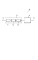
図1は、本実施形態に係る利得等化器10の構成図である。この図に示される利得等化器10は、入力端10aに入力した光のスペクトルを所定の波長範囲で平坦化して出力端10bから出力するものであり、入力端10aと出力端10bとの間に直列的に接続された概略等化部11および微調等化部12を備えている。概略等化部11および微調等化部12のうち何れが前段に設けられてもよい。
【0017】
概略等化部11は、所定の波長範囲で光のスペクトルを概略的に平坦化する。この概略等化部11は微調等化部12と比較して付与損失が大きく反射が小さいフィルタ111〜113で構成されており、これにより、利得等化器10全体からの光の反射が抑制される。また、概略等化部11に含まれる光フィルタ111〜113それぞれは、長周期グレーティング、スラント型グレーティング、誘電体多層膜フィルタおよびエタロンフィルタの何れかであるのが好適である。
【0018】
微調等化部12は、所定の波長範囲のうち概略等化部11により所定値以下に平坦化できない波長範囲で光のスペクトルを更に平坦化する。この微調等化部12は、最小帯域幅が狭いスラント型グレーティングおよびチャープ型グレーティングの何れかを1または複数含むのが好適である。
【0019】
また、所定の波長範囲において概略等化部11により平坦化したときの残差の周期が、微調等化部12の最小帯域幅より広いのが好適である。このようにすることにより、微調等化部12による光スペクトルの更なる平坦化が容易となる。
【0020】
図2は、長周期グレーティングの構成図である。この図に示される長周期グレーティング200は、概略等化部11に含まれるフィルタとして好適に用いられ得るものである。長周期グレーティング200は、コア領域211およびクラッド領域212を有する光ファイバ210の長手方向に沿った一定範囲において、屈折率変調による回折格子213がコア領域211に形成されたものである。長周期グレーティング200は、回折格子213の格子間隔が長く数百μmであり、コア領域211を伝搬してきて回折格子213に到達した導波モード光のうち、クラッドモード光との間で位相整合条件を満たす波長の光に対して損失を付与する。
【0021】
図3は、スラント型グレーティングの構成図である。この図に示されるスラント型グレーティング300は、概略等化部11または微調等化部12に含まれるフィルタとして好適に用いられ得るものである。スラント型グレーティング300は、コア領域311およびクラッド領域312を有する光ファイバ310の長手方向に沿った一定範囲において、屈折率変調による回折格子313がコア領域311に形成されたものである。スラント型グレーティング300は、回折格子313の格子間隔が狭く、回折格子313の格子面が光ファイバ310の光軸に対して傾斜している。スラント型グレーティング300は、コア領域311を伝搬してきて回折格子313に到達した導波モード光のうち、回折格子313におけるブラッグ条件を満たす波長より短波長側の光に対して損失を付与する。
【0022】
図4は、チャープ型グレーティングの構成図である。この図に示されるチャープ型グレーティング400は、微調等化部12に含まれるフィルタとして好適に用いられ得るものである。チャープ型グレーティング400は、コア領域411およびクラッド領域412を有する光ファイバ410の長手方向に沿った一定範囲において、屈折率変調による回折格子413がコア領域411に形成されたものである。チャープ型グレーティング400は、回折格子413の格子間隔が狭く、回折格子413の格子間隔が長手方向に沿って次第に変化している。チャープ型グレーティング400は、コア領域411を伝搬してきて回折格子413に到達した導波モード光のうち、回折格子413の長手方向の各位置におけるブラッグ条件を満たす波長の光に対して損失を付与する。
【0023】
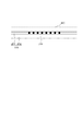
図5は、本実施形態に係る利得等化器10の透過スペクトル等を示す図である。この図には、フィルタ111の透過率T111、フィルタ112の透過率T112、フィルタ113の透過率T113、微調等化部12の透過率T12、利得等化器10全体の実際の透過率T10、利得等化器10全体の目標の透過率Ttarget および 誤差ΔT(=Ttarget−T10) それぞれのスペクトルが示されている。なお、概略等化部11に含まれるフィルタ111〜113それぞれが長周期グレーティングであるとし、微調等化部12がスラント型グレーティングであるとした。この図に示されるように、Cバンド(1530nm〜1565nm)において、誤差ΔTが−0.02dB〜+0.01dBの範囲にあり、利得等化器10全体の実際の透過率T10は目標透過率Ttargetとよく一致した。
【0024】
本実施形態に係る利得等化器10は、付与損失が大きくても精度よく光スペクトルを等化することができ、また、最小帯域幅が広いものでも概略等化部11のフィルタとして使用することができる。概略等化部11により所定値以下に平坦化できない波長範囲で光のスペクトルを微調等化部12により更に平坦化するので、概略等化部11の等化精度は高くなくてもよく、それ故、利得等化器10が製造容易で安価なものとなる。最小帯域幅が狭いフィルタ単体で大きな損失を付与するよりも、そのようなフィルタを微調等化部12に使用する方が等化精度が向上する。また、スラント型グレーティングやチャープト型グレーティングは、他のタイプのフィルタと比較して最小帯域幅が狭いが反射率が大きいので、付与損失が小さい微調等化部12として用いられることにより、利得等化器10全体の反射が小さくなる。
【0025】
図6は、第1実施形態に係る光増幅装置1の構成図である。この図に示される光増幅装置1は、入力端1aに入力した所定の波長範囲内の信号光を光増幅して出力端1bから出力するものであり、入力端1aから出力端1bに向かって順に光増幅器20、光アイソレータ30、微調等化部12および概略等化部11を備えている。微調等化部12および概略等化部11は、本実施形態に係る等化部10に含まれる。
【0026】
光増幅器20は、入力端1aに入力した所定の波長範囲内の信号光を光増幅して、その光増幅した信号光を光アイソレータ30へ出力する。光増幅器20は、光増幅用ファイバ21、光カプラ22および励起光源23を有している。光増幅用ファイバ21は、希土類元素(例えばEr元素)がコア領域に添加された光ファイバであり、その希土類元素を励起し得る波長の励起光が供給されることで、所定の波長範囲内の信号光を光増幅する。励起光源23は、光増幅用ファイバ21へ供給すべき励起光を出力する。光カプラ22は、励起光源23より出力された励起光を光増幅用ファイバ21へ出力するとともに、光増幅用ファイバ21により光増幅された信号光を光アイソレータ30へ出力する。光増幅用ファイバ21がEr元素添加光ファイバである場合には、励起光の波長は0.98μmまたは1.48μmであり、光増幅される信号光の波長域はCバンドである。
【0027】
光アイソレータ30は、光増幅器20と利得等化器10との間に設けられ、入力端1aから出力端1bに向かう順方向のみに光を通過させ、逆方向には光を通過させない。利得等化器10は、上述した本実施形態に係るものであり、光増幅器20により光増幅された後に光アイソレータ30を通過した信号光のスペクトルを所定の波長範囲で平坦化して、その信号光を出力端1bより出力する。
【0028】
この光増幅装置1では、入力端1aに入力した所定の波長範囲の信号光は、光増幅器20の光増幅用ファイバ21において光増幅された後に、光アイソレータ30を通過して、利得等化器10により利得等化される。この光増幅装置1全体の利得スペクトルは、光増幅器20の利得スペクトルと利得等化器10の透過スペクトルとを総合したものとなる。光増幅器20の利得スペクトルを目標として、利得等化器10の損失スペクトルが設計され、各フィルタの透過スペクトルが設計されて、これにより、光増幅装置1の全体の利得スペクトルは所定の波長範囲で平坦化される。
【0029】
光アイソレータ30から利得等化器10へ入射した光の一部は利得等化器10により反射される場合があり、その反射光は利得等化器10から光アイソレータ30へ向かう。もし、光アイソレータ30が設けられていないとすると、反射光は光増幅器20に入射して光増幅され、その光増幅された反射光は更に上流に向かって伝搬してき、信号光の伝送品質に悪影響を与える。しかし、第1実施形態では、光アイソレータ30が設けられていることにより、反射光が光アイソレータ30を通過して光増幅器20へ入射することは無いので、信号光の伝送品質が劣化することが無い。
【0030】
また、本実施形態のように、利得等化器10において、反射率が比較的大きい微調等化部12を前段に配置し、反射率が比較的小さい概略等化部11を後段に配置するのが好適である。このように、反射率が大きい微調等化部12を光アイソレータ30の直後に配置することにより、下流側からのレイリ散乱に因る反射光を利得等化器10で反射して再び下流に出力されてしまうノイズ成分を小さくすることができる。反射が小さく損失が大きい概略等化部11を2回通過させることで微調等化部12の反射の影響を低減できるからである。
【0031】
図7は、第2実施形態に係る光増幅装置2の構成図である。この図に示される光増幅装置2は、入力端2aに入力した所定の波長範囲内の信号光を光増幅して出力端2bから出力するものであり、入力端2aから出力端2bに向かって順に光増幅器20、概略等化部11および微調等化部12を備えている。概略等化部11および微調等化部12は、本実施形態に係る等化部10に含まれる。
【0032】
第1実施形態に係る光増幅装置1と比較すると、第2実施形態に係る光増幅装置2は、光増幅器20と利得等化器10との間に光アイソレータが設けられていない点、および、利得等化器10において概略等化部11が前段に設けられ微調等化部12が後段に設けられている点、で相違する。この光増幅装置2は、光アイソレータを設ける必要がないので、安価なものとなる。
【0033】
この光増幅装置2では、入力端2aに入力した所定の波長範囲の信号光は、光増幅器20の光増幅用ファイバ21において光増幅された後に、利得等化器10により利得等化される。この光増幅装置2全体の利得スペクトルは、光増幅器20の利得スペクトルと利得等化器10の透過スペクトルとを総合したものとなる。光増幅器20の利得スペクトルを目標として、利得等化器10の損失スペクトルが設計され、各フィルタの透過スペクトルが設計されて、これにより、光増幅装置2の全体の利得スペクトルは所定の波長範囲で平坦化される。
【0034】
利得等化器10へ入射した光の一部は、利得等化器10に含まれる概略等化部11および微調等化部12それぞれにより反射される場合があり、その反射光は上流側へ向かう。しかし、第2実施形態では、光増幅器20と利得等化器10との間に光アイソレータが設けられていないものの、利得等化器10において、反射率が比較的小さい概略等化部11が前段に設けられ、反射率が比較的大きい微調等化部12が後段に設けられていることにより、微調等化部12に因る反射光が概略等化部11により損失を被るので、増幅器20への反射光の入射が低減され、信号光の伝送品質の劣化が低減される。本構成は、下流側への反射の影響があまり重要ではなく低コストが重要なシステムに用いると好適である。
【0035】
【発明の効果】
以上、詳細に説明したとおり、本発明によれは、入力した光のスペクトルに対して、所定の波長範囲で概略等化部により概略的に平坦化し、所定の波長範囲のうち概略等化部により所定値以下に平坦化できない波長範囲で微調等化部により更に平坦化するので、良好な等化特性を有する。そして、概略等化部が微調等化部と比較して付与損失が大きく反射が小さいフィルタで構成されていることにより、良好な等化特性を有するものが容易に製造され得る。
【図面の簡単な説明】
【図1】本実施形態に係る利得等化器10の構成図である。
【図2】長周期グレーティングの構成図である。
【図3】スラント型グレーティングの構成図である。
【図4】チャープ型グレーティングの構成図である。
【図5】本実施形態に係る利得等化器10の透過スペクトル等を示す図である。
【図6】第1実施形態に係る光増幅装置1の構成図である。
【図7】第2実施形態に係る光増幅装置2の構成図である。
【図8】フィルタ単体の透過スペクトルの1例を示す図である。
【図9】利得等化器の透過スペクトルの1例を示す図である。
【図10】フィルタの最小帯域幅、利得等化器における信号光波長帯域幅および利得等化残差の1例を纏めた図表である。
【符号の説明】
1,2…光増幅装置、10…利得等化器、11…概略等化部、12…微調等化部、20…光増幅器、21…光増幅用ファイバ、22…光カプラ、2…励起光源、30…光アイソレータ、111〜113…フィルタ。[0001]
TECHNICAL FIELD OF THE INVENTION
The present invention relates to a gain equalizer for flattening an input light spectrum in a predetermined wavelength range and outputting the same, and an optical amplifying device for optically amplifying and outputting signal light in a predetermined wavelength range.
[0002]
[Prior art]
The optical amplifying device optically amplifies signal light input to an input terminal and outputs the amplified signal light from an output terminal, and is used in, for example, a wavelength multiplexing optical communication system. Such an optical amplifier is required to have a flat gain spectrum in a predetermined wavelength range. However, the gain spectrum of an optical amplification medium (for example, an Er element-doped optical fiber) generally used in an optical amplification device is not flat.
[0003]
Therefore, the optical amplifying apparatus is also provided with a gain equalizer having a loss spectrum having substantially the same shape as the gain spectrum of the optical amplifying medium, and integrates the gain spectrum of the optical amplifying medium and the transmission spectrum of the gain equalizer. The obtained overall gain spectrum is flattened in a predetermined wavelength range. As the gain equalizer, a filter including a filter such as a long-period grating (for example, see Non-Patent Document 1) or a slant-type grating (for example, see
[0004]
The transmission spectrum of a single filter such as a long-period grating or a slanted grating has a shape as shown in FIG. FIG. 8 is a diagram illustrating an example of the transmission spectrum of the filter alone. In the figure, the transmission spectrum of the filter A has a bandwidth of 10 nm (hereinafter referred to as a “minimum bandwidth”) in which the transmittance is −0.1 dB or less. The transmission spectrum of the filter B has a minimum bandwidth of 6 nm. In general, a gain equalizer is configured by connecting a plurality of filters having such a transmission spectrum shape and having different minimum transmittances, minimum transmittance wavelengths, and minimum bandwidths in series. FIG. 9 is a diagram illustrating an example of a transmission spectrum of the gain equalizer. This figure shows a target transmission spectrum of the gain equalizer, an actual transmission spectrum when a plurality of filters are used, and an error between the target transmittance and the actual transmittance.
[0005]
[Patent Document 1]
Japanese Patent Application Laid-Open No. 2002-82235 [Non-Patent Document 1]
Ash M. Vengsarkar, et al. , "Long-Period Fiber Gratings as Band-Rejection Filters", Journal of Lightwave Technology, Vol. 14, No. 1, pp. 58-65 (1996)
[Non-patent document 2]
See Isabelle Riant, et al. , "36 nm Amplifier Gain Equalizer Based on Slant Bragg Grating Technology for Multichannel Transmission", Suboptic 2001, P4.3.10 (2001).
[0006]
[Problems to be solved by the invention]
However, the actual gain equalization characteristics of the gain equalizer when a plurality of filters are used depend on the minimum bandwidth of the filter used and the width of the signal light wavelength band to be gain-equalized. FIG. 10 is a table summarizing one example of design values of the minimum bandwidth of the filter, the signal light wavelength bandwidth in the gain equalizer, and the gain equalization residual. If the signal light wavelength bandwidth is 40 nm, the gain equalization residual is 0.12 dB if the minimum bandwidth of the filter is 10 nm, and the gain equalization residual is 0 if the minimum bandwidth of the filter is 6 nm. 0.06 dB. Also, when the signal light wavelength bandwidth is 30 nm, the gain equalization residual is 0.05 dB when the minimum bandwidth of the filter is 10 nm, and the gain equalization residual when the minimum bandwidth of the filter is 6 nm. Is 0.02 dB. Thus, if the minimum bandwidth of the filter is wide, the gain equalization characteristics of the gain equalizer are poor. To realize a gain equalizer having good gain equalization characteristics, it is preferable to use a filter having a narrow minimum bandwidth. However, on the other hand, if the minimum bandwidth of the filter is narrow, it is difficult to manufacture a filter having a large maximum loss with high accuracy.
[0007]
The present invention has been made in order to solve the above problems, and provides a gain equalizer that has good equalization characteristics and is easy to manufacture, and an optical amplifying device including the gain equalizer. With the goal.
[0008]
[Means for Solving the Problems]
A gain equalizer according to the present invention is a gain equalizer that flattens an input light spectrum in a predetermined wavelength range and outputs the flattened spectrum, and a general equalizer that flattens the light spectrum in a predetermined wavelength range. And a fine adjustment equalizer for flattening the spectrum of light in a wavelength range that cannot be flattened to a predetermined value or less by the general equalizer in the predetermined wavelength range, and the general equalizer is compared with the fine equalizer. And a filter having a large applied loss and a small reflection.
[0009]
This gain equalizer roughly flattens the spectrum of the input light in a predetermined wavelength range by a rough equalizer, and cannot flatten the spectrum of the input light to a predetermined value or less in the rough wavelength equalizer. Since it is further flattened in the wavelength range by the fine adjustment equalizer, it has good equalization characteristics. Since the gain equalizer is composed of a filter having a large applied loss and a small reflection as compared with the fine adjustment equalizer, the gain equalizer having a good equalization characteristic can be easily manufactured. Can be done.
[0010]
In the gain equalizer according to the present invention, the period of the residual when flattened by the general equalizer in the predetermined wavelength range is smaller than the bandwidth of the band where the transmittance of the fine equalizer is −0.1 dB or less. Wide is preferred. In this case, the gain equalizer may have better equalization characteristics.
[0011]
In the gain equalizer according to the present invention, it is preferable that the general equalizer includes any one of a long-period grating, a slanted grating, a dielectric multilayer filter, and an etalon filter. Further, it is preferable that the fine adjustment equalizing section includes one of a slant type grating and a chirp type grating.
[0012]
An optical amplifying device according to the present invention is an optical amplifying device for optically amplifying signal light within a predetermined wavelength range input to an input terminal and outputting the signal light from an output terminal, and optically amplifies the signal light within a predetermined wavelength range. And a gain equalizer according to the present invention for flattening the spectrum of the signal light optically amplified by the optical amplifier in a predetermined wavelength range and outputting the flattened spectrum.
[0013]
This optical amplifying device optically amplifies signal light in a predetermined wavelength range by an optical amplifier, flattens the spectrum of the optically amplified signal light in a predetermined wavelength range by a gain equalizer, and outputs the flattened signal light. The overall gain spectrum of the optical amplifying apparatus is a sum of the gain spectrum of the optical amplifier and the transmission spectrum of the gain equalizer, and has excellent flatness in a predetermined wavelength range.
[0014]
The optical amplifier according to the present invention is preferably provided with an optical isolator that allows light to pass only in the forward direction from the input terminal to the output terminal between the optical amplifier and the gain equalizer, and at this time, It is preferable that an optical amplifier, an optical isolator, a fine adjustment equalizer, and a general equalizer are arranged in order from the input terminal to the output terminal. In the optical amplifying device according to the present invention, an optical amplifier, a general equalizer, and a fine equalizer are arranged in order from the input end to the output end, and light is emitted only in the forward direction from the input end to the output end. Is preferably not provided between the optical amplifier and the gain equalizer.
[0015]
BEST MODE FOR CARRYING OUT THE INVENTION
Hereinafter, embodiments of the present invention will be described in detail with reference to the accompanying drawings. In the description of the drawings, the same elements will be denoted by the same reference symbols, without redundant description.
[0016]
FIG. 1 is a configuration diagram of a
[0017]
The
[0018]
The
[0019]
Further, it is preferable that the cycle of the residual when flattened by the
[0020]
FIG. 2 is a configuration diagram of the long period grating. The long-period grating 200 shown in this figure can be suitably used as a filter included in the
[0021]
FIG. 3 is a configuration diagram of a slant type grating. The
[0022]
FIG. 4 is a configuration diagram of a chirped grating. The chirped grating 400 shown in this figure can be suitably used as a filter included in the
[0023]
FIG. 5 is a diagram showing a transmission spectrum and the like of the
[0024]
The
[0025]
FIG. 6 is a configuration diagram of the
[0026]
The
[0027]
The
[0028]
In the
[0029]
A part of the light incident on the
[0030]
Further, as in the present embodiment, in the
[0031]
FIG. 7 is a configuration diagram of the
[0032]
Compared to the
[0033]
In the
[0034]
A part of the light incident on the
[0035]
【The invention's effect】
As described in detail above, according to the present invention, the spectrum of the input light is roughly flattened by the rough equalizer in a predetermined wavelength range, and is roughly flattened by the rough equalizer in a predetermined wavelength range. Since the flattening is further performed by the fine adjustment equalizing portion in a wavelength range where the flattening cannot be performed below a predetermined value, it has good equalizing characteristics. And since an approximate equalization part is comprised by the filter which has a large provisional loss and a small reflection compared with a fine adjustment equalization part, what has a favorable equalization characteristic can be manufactured easily.
[Brief description of the drawings]
FIG. 1 is a configuration diagram of a
FIG. 2 is a configuration diagram of a long period grating.
FIG. 3 is a configuration diagram of a slanted grating.
FIG. 4 is a configuration diagram of a chirped grating.
FIG. 5 is a diagram showing a transmission spectrum and the like of the
FIG. 6 is a configuration diagram of the
FIG. 7 is a configuration diagram of an
FIG. 8 is a diagram illustrating an example of a transmission spectrum of a filter alone.
FIG. 9 is a diagram illustrating an example of a transmission spectrum of a gain equalizer.
FIG. 10 is a table summarizing one example of a minimum bandwidth of a filter, a signal light wavelength bandwidth in a gain equalizer, and a gain equalization residual;
[Explanation of symbols]
Claims (8)
前記所定の波長範囲で前記光のスペクトルを平坦化する概略等化部と、
前記所定の波長範囲のうち前記概略等化部により所定値以下に平坦化できない波長範囲で前記光のスペクトルを平坦化する微調等化部と
を備え、
前記概略等化部は前記微調等化部と比較して付与損失が大きく反射が小さいフィルタで構成されている
ことを特徴とする利得等化器。A gain equalizer that flattens and outputs a spectrum of input light in a predetermined wavelength range,
A general equalizer for flattening the spectrum of the light in the predetermined wavelength range,
A fine-tuning equalizer that flattens the spectrum of the light in a wavelength range that cannot be flattened to a predetermined value or less by the general equalizer in the predetermined wavelength range,
A gain equalizer characterized in that the general equalizer comprises a filter having a larger applied loss and a smaller reflection compared to the fine adjustment equalizer.
前記所定の波長範囲内の信号光を光増幅して出力する光増幅器と、
前記光増幅器により光増幅された信号光のスペクトルを前記所定の波長範囲で平坦化して出力する請求項1記載の利得等化器と
を備えることを特徴とする光増幅装置。An optical amplifier that optically amplifies signal light within a predetermined wavelength range input to an input terminal and outputs the amplified signal light from an output terminal,
An optical amplifier that optically amplifies and outputs the signal light within the predetermined wavelength range,
2. An optical amplifying apparatus comprising: the gain equalizer according to claim 1, wherein the spectrum of the signal light optically amplified by the optical amplifier is flattened in the predetermined wavelength range and output.
前記入力端から前記出力端に向かう順方向のみに光を通過させる光アイソレータが前記光増幅器と前記利得等化器との間に設けられていない
ことを特徴とする請求項5記載の光増幅装置。The optical amplifier, the general equalizer, and the fine-tuning equalizer are arranged in order from the input end toward the output end,
6. The optical amplifying device according to claim 5, wherein an optical isolator that passes light only in a forward direction from the input terminal to the output terminal is not provided between the optical amplifier and the gain equalizer. .
Priority Applications (2)
| Application Number | Priority Date | Filing Date | Title |
|---|---|---|---|
| JP2002276032A JP2004109928A (en) | 2002-09-20 | 2002-09-20 | Gain equalizer and light amplifier |
| US10/665,357 US6952511B2 (en) | 2002-09-20 | 2003-09-22 | Gain equalizer and optical amplification apparatus |
Applications Claiming Priority (1)
| Application Number | Priority Date | Filing Date | Title |
|---|---|---|---|
| JP2002276032A JP2004109928A (en) | 2002-09-20 | 2002-09-20 | Gain equalizer and light amplifier |
Publications (1)
| Publication Number | Publication Date |
|---|---|
| JP2004109928A true JP2004109928A (en) | 2004-04-08 |
Family
ID=32272041
Family Applications (1)
| Application Number | Title | Priority Date | Filing Date |
|---|---|---|---|
| JP2002276032A Pending JP2004109928A (en) | 2002-09-20 | 2002-09-20 | Gain equalizer and light amplifier |
Country Status (2)
| Country | Link |
|---|---|
| US (1) | US6952511B2 (en) |
| JP (1) | JP2004109928A (en) |
Cited By (2)
| Publication number | Priority date | Publication date | Assignee | Title |
|---|---|---|---|---|
| US8760628B2 (en) | 2011-01-01 | 2014-06-24 | Canon Kabushiki Kaisha | Filter, exposure apparatus, and method of manufacturing device |
| JP2018036400A (en) * | 2016-08-30 | 2018-03-08 | 株式会社フジクラ | Fiber-chirped grating element and fiber laser |
Families Citing this family (1)
| Publication number | Priority date | Publication date | Assignee | Title |
|---|---|---|---|---|
| JP2004109928A (en) * | 2002-09-20 | 2004-04-08 | Sumitomo Electric Ind Ltd | Gain equalizer and light amplifier |
Family Cites Families (6)
| Publication number | Priority date | Publication date | Assignee | Title |
|---|---|---|---|---|
| US5920424A (en) * | 1997-02-18 | 1999-07-06 | Lucent Technologies Inc. | Article comprising a broadband optical fiber amplifier |
| US5982791A (en) * | 1998-01-14 | 1999-11-09 | Hewlett-Packard Company | Wavelength tracking in adjustable optical systems |
| JP2003524931A (en) * | 1999-03-11 | 2003-08-19 | ピレリー・サブマリン・テレコム・システムズ・イタリア・ソチエタ・ペル・アツィオーニ | Multi-wavelength optical communication system with optical amplifier |
| JP2002082235A (en) | 2000-06-19 | 2002-03-22 | Fujikura Ltd | Slant type short period grating |
| US6636666B2 (en) * | 2001-05-14 | 2003-10-21 | University Of Iowa Research Foundation | Optical power equalizer |
| JP2004109928A (en) * | 2002-09-20 | 2004-04-08 | Sumitomo Electric Ind Ltd | Gain equalizer and light amplifier |
-
2002
- 2002-09-20 JP JP2002276032A patent/JP2004109928A/en active Pending
-
2003
- 2003-09-22 US US10/665,357 patent/US6952511B2/en not_active Expired - Fee Related
Cited By (3)
| Publication number | Priority date | Publication date | Assignee | Title |
|---|---|---|---|---|
| US8760628B2 (en) | 2011-01-01 | 2014-06-24 | Canon Kabushiki Kaisha | Filter, exposure apparatus, and method of manufacturing device |
| JP2018036400A (en) * | 2016-08-30 | 2018-03-08 | 株式会社フジクラ | Fiber-chirped grating element and fiber laser |
| WO2018043289A1 (en) * | 2016-08-30 | 2018-03-08 | 株式会社フジクラ | Chirped fiber grating element and fiber laser |
Also Published As
| Publication number | Publication date |
|---|---|
| US6952511B2 (en) | 2005-10-04 |
| US20040109638A1 (en) | 2004-06-10 |
Similar Documents
| Publication | Publication Date | Title |
|---|---|---|
| JP3377728B2 (en) | Device consisting of optical waveguide | |
| US5636301A (en) | Optical waveguide amplifiers | |
| JP3749392B2 (en) | Articles including improved cascaded fiber optic Raman devices | |
| EP0559356B1 (en) | Optical repeaters | |
| US5978131A (en) | In-fiber two-stage amplifier providing WDM signal conditioning | |
| US5598294A (en) | Optical fiber amplifier and optical fiber communication system | |
| EP1569020B1 (en) | Optical multiplexing method and optical multiplexer, and optical amplifier using the same | |
| US6222962B1 (en) | Optical amplifier | |
| JPH10133054A (en) | Article that includes optical waveguide | |
| JPH05224158A (en) | Optical filter and light amplifier using the same | |
| US10297971B2 (en) | Optical amplifier | |
| JPH1172630A (en) | Process for producing chirp type optical fiber grating | |
| US6674773B1 (en) | Multi-wavelength Raman laser | |
| US6498676B1 (en) | Optical filter for use or with an optical amplifier | |
| JP2000321421A (en) | Optical resonance cavity, optical filter and etalon optical filter device as well as optical amplifier using the same and a method for controlling gain tilt of amplifier beam | |
| US6738183B2 (en) | Optical filter functioning as both a gain equalizer and noise-light blocking filter | |
| JP3325459B2 (en) | Optical filter module, optical amplifier, and optical transceiver | |
| EP1101261A2 (en) | Thermal tuning of optical amplifiers and use of same in wavelength division multiplexed systems | |
| US6404539B1 (en) | Light source for optical data transmission | |
| KR100438426B1 (en) | Unpolarized multi lambda source | |
| JP2004109928A (en) | Gain equalizer and light amplifier | |
| WO2002093704A1 (en) | Optical fiber and system containing same | |
| JP3129368B2 (en) | Optical signal transmission method and relay amplifier | |
| JP3203641B2 (en) | Optical loss filter | |
| US7495825B2 (en) | Integration of a gain equalization filter in a gain medium |
Legal Events
| Date | Code | Title | Description |
|---|---|---|---|
| A621 | Written request for application examination |
Free format text: JAPANESE INTERMEDIATE CODE: A621 Effective date: 20050330 |
|
| A131 | Notification of reasons for refusal |
Free format text: JAPANESE INTERMEDIATE CODE: A131 Effective date: 20080219 |
|
| A02 | Decision of refusal |
Free format text: JAPANESE INTERMEDIATE CODE: A02 Effective date: 20080624 |