JP2004088715A - High frequency switch and electronic device using it - Google Patents
High frequency switch and electronic device using it Download PDFInfo
- Publication number
- JP2004088715A JP2004088715A JP2002350087A JP2002350087A JP2004088715A JP 2004088715 A JP2004088715 A JP 2004088715A JP 2002350087 A JP2002350087 A JP 2002350087A JP 2002350087 A JP2002350087 A JP 2002350087A JP 2004088715 A JP2004088715 A JP 2004088715A
- Authority
- JP
- Japan
- Prior art keywords
- electrode
- stub
- line electrode
- frequency switch
- frequency
- Prior art date
- Legal status (The legal status is an assumption and is not a legal conclusion. Google has not performed a legal analysis and makes no representation as to the accuracy of the status listed.)
- Granted
Links
Images


Classifications
-
- H—ELECTRICITY
- H01—ELECTRIC ELEMENTS
- H01P—WAVEGUIDES; RESONATORS, LINES, OR OTHER DEVICES OF THE WAVEGUIDE TYPE
- H01P1/00—Auxiliary devices
- H01P1/10—Auxiliary devices for switching or interrupting
- H01P1/15—Auxiliary devices for switching or interrupting by semiconductor devices
Landscapes
- Junction Field-Effect Transistors (AREA)
- Waveguide Switches, Polarizers, And Phase Shifters (AREA)
- Semiconductor Integrated Circuits (AREA)
- Oscillators With Electromechanical Resonators (AREA)
- Electrotherapy Devices (AREA)
Abstract
Description
【0001】
【発明の属する技術分野】
本発明は、高周波スイッチおよびそれを用いた電子装置、特にミリ波帯の信号のスイッチングに用いられる高周波スイッチおよびそれを用いた電子装置に関する。
【0002】
【従来の技術】
ミリ波帯の信号の切換などに用いられるスイッチとしては、一般にPINダイオードを用いたスイッチが使用されるが、比較的低い周波数においてはFETを用いたスイッチが使用されることもある。その中でも、特に高周波信号の通る線路そのものをFETのドレインやソースとして利用するスイッチがあり、例えば特許文献1、特許文献2、特許文献3、特許文献4などに具体例が開示されている。
【0003】
特許文献1(従来例1)には、信号線路を、その幅方向に横切る複数のスリットで複数のドレイン用電極に分割するとともに、そのスリットに同じく信号線路の幅方向に伸びるソース用電極とゲート用電極(線路)を形成することによって、信号線路の一部をFETとして用いる高周波スイッチが開示されている(例えば図13)。なお、各ドレイン用電極は金属配線により接続される。そして、FETのドレイン・ソース間には、信号周波数においてFETのオフ容量と並列共振するインダクタンス素子が接続されている。
【0004】
従来例1においては、信号線路そのものはFETが形成されている部分も含めて直流的には常に導通状態にある。そして、FETがオン状態になることによって、信号線路とグランド間に接続された回路のインピーダンスが小さくなってほぼ短絡状態になる。その結果、信号線路の一部が略接地状態となって高周波信号は反射され、導通が阻止される。逆にFETがオフの時には、FETのオフ容量とインダクタンス素子との並列共振によって、信号線路とグランド間に接続された回路の高周波信号の周波数におけるインピーダンスが無限大になる。これは、高周波信号の周波数においては信号線路に何も接続されていないことを意味するので、高周波信号は導通する。このようにしてスイッチ動作がなされる。
【0005】
特許文献2(従来例2)には、信号線路の一部(ドレイン電極として機能する)において、その長手方向に沿って隣接してグランド電極(ソース電極として機能する)が形成され、両者の隙間に信号線路の長手方向に沿って伸びるゲート電極が形成された高周波スイッチが開示されている(例えば図6)。
【0006】
従来例2においては、FETがオフの時には、ドレインとして動作する信号線路の一部は単なる信号線路として動作するために、高周波信号は信号線路を導通する。一方、FETがオンの時には、ドレインとして動作する信号線路の一部はグランド電極と接続されることになるため、信号線路の一部が実質的に接地されたことになり、高周波信号は反射され、導通が阻止される。
【0007】
特許文献3(従来例3)には、従来例1と同様のFET構成(図8、並列共振用のインダクタンス素子はない)と、同様の構成でFETのドレイン、ソース、ゲートが信号線路の線路方向に伸びるように構成したもの(図1)が開示されている。
【0008】
従来例3においても、FETのオン時に信号線路の一部が実質的に接地状態になって高周波信号を阻止するという点で、従来例2と同様の動作が行われる。
【0009】
そして、特許文献4(従来例4)には、信号線路の主線路に1/4波長のスタブを接続し、さらにスタブの先端をドレイン電極とするとともにソース電極を接地してFETを形成したもの(図2、図6)が開示されている。そして、FETをオン、オフすることによってスタブを1/4波長のショートスタブあるいはオープンスタブとして動作させている。
【0010】
従来例4においても、FETのオフ時にスタブが1/4波長のオープンスタブになり、信号線路の一部が高周波信号の周波数において実質的に接地状態になって高周波信号を阻止するという点で、従来例2や3と同様の動作が行われる。
【0011】
【特許文献1】
特開平6−232601号公報
【特許文献2】
特開平10−41404号公報
【特許文献3】
特開2000−294568号公報
【特許文献4】
特開2000−332502号公報
【0012】
【発明が解決しようとする課題】
ところで、従来例1においては、FETのオン時の導通抵抗を小さくする必要があるが、そのためには信号線路の分割数を増やしてゲート電極の数を増やしてFETの総ゲート幅を大きくする必要がある。総ゲート幅を大きくすると必然的にFETのオフ容量が大きくなるために、それにしたがって並列共振のためのインダクタンス素子のインダクタンス値を小さくする必要がある。しかしながら、インダクタンス値の精度を保ったままインダクタンス素子の形状を小さくするのには限界がある。そして、信号周波数が高くなるほどインダクタンス値を小さくする必要があるため、この構成は信号周波数が高くなるほど使用しにくくなるという問題を含んでいる。
【0013】
一方、従来例2においては、共振現象を利用していないために上記のような信号周波数が高くなると使用しにくくなるという問題はない。しかしながら、従来例1においては、信号線路の中のスイッチオン時に高周波信号が流れる主線路自身がFETのドレイン電極となっている。ドレイン電極は少なくとも一部が半導体活性層上に形成されるために、これは主線路の一部が半導体活性層上に形成されるということを意味する。この半導体活性層にも線路の一部として高周波信号が流れるが、半導体活性層はドレイン電極に比べると抵抗の高い導体であるために、これは主線路の抵抗が大きくなることを意味する。したがって、従来例1のような主線路自身がFETのドレイン電極になっているスイッチにおいては、それが主線路の挿入損失を増加させる原因になるという問題もある。
【0014】
また、FETの単位長さあたり(単位ゲート幅あたり)のオン抵抗は、FETの断面構造を変更することで低減することができるが、これは必ずしも容易ではない。そして、単位長さあたりのオン抵抗を変えられない場合には、FETオン時に主線路を十分に接地させるためにはFETのゲート幅を大きくする必要がある。FETのゲート幅を大きくするということは信号線路の長手方向にゲート電極を伸ばすということを意味し、これは同時にドレイン電極が長くなることを意味する。これはスイッチが主線路の長手方向に大型化することを意味する。そして、ドレイン電極は半導体活性層上に形成された高周波信号が流れる主線路でもあるため、上述したような主線路の挿入損失を増加させる傾向をさらに強めることになる。
【0015】
次に、従来例3は、従来例1と基本的な構成は同じであり、同様の問題を有している。
【0016】
最後に、従来例4においては、高周波信号の流れる主線路はドレイン電極にはなっていないので、スイッチオン時の挿入損失が増えるという問題はない。しかしながら、スタブの端部を十分に低い抵抗値で接地させるためにはFETのゲート幅を長くする必要がある。そして、FETのゲート幅を長くすると、FETのオフ時におけるドレイン・ソース間の容量が増える。これは、FETのオフ時にオープンスタブの先端とグランドとの間に大きな容量が存在することを意味する。オープンスタブの先端に大きな容量が存在すると、オープンスタブの共振周波数は低下するため、ショートスタブのときの共振周波数とは異なるものになる可能性が高い。オープンスタブとショートスタブの共振周波数を同じにできないということはスイッチとして正常に機能しないということを意味し、大きな問題となる。
【0017】
本発明は上記の問題点を解決することを目的とするもので、高い周波数まで利用でき、スイッチオン時の挿入損失が少なく、しかもスイッチオフ時の信号遮断性能の高い高周波スイッチおよびそれを用いた電子装置を提供する。
【0018】
【課題を解決するための手段】
上記目的を達成するために、本発明の高周波スイッチは、2つの端子間に設けられた主線路電極と、一端が前記主線路電極の側縁に接続されるとともに他端が接地されたスタブ線路電極と、該スタブ線路電極の幅方向に隣接して設けられたグランド電極とを備え、
前記スタブ線路電極の少なくとも一端側の側縁と前記グランド電極の間の基板部分に、前記スタブ線路電極および前記グランド電極の下まで延在する半導体活性層が形成されるとともに、前記スタブ線路電極および前記グランド電極の間の前記半導体活性層上に前記スタブ線路電極の長手方向に沿って伸びるゲート電極が設けられることによってFET構造が形成されていることを特徴とする。
【0019】
さらには、前記スタブ線路電極の一端側から他端側までの側縁と前記グランド電極の間の基板部分に、前記スタブ線路電極および前記グランド電極の下まで延在する半導体活性層が形成されるとともに、前記スタブ線路電極および前記グランド電極の間の前記半導体活性層上に前記スタブ線路電極の長手方向に沿って伸びるゲート電極が設けられることによってFET構造が形成されていることを特徴とする。
【0020】
また、前記FET構造が、前記スタブ線路電極の両側縁に形成されていることを特徴とする。
【0021】
また、前記FET構造の形成されたスタブ線路電極は、前記グランド電極とともにコプレーナウェーブガイドを形成していることを特徴とする。
【0022】
そして、前記FET構造の形成されたスタブ線路電極は、流れる高周波信号に対して略90°の電気長になるように形成されていることを特徴とする。
【0023】
また、本発明の高周波スイッチは、複数の前記FET構造の形成されたスタブ線路電極の一端が、前記主線路電極の側縁に接続されていることを特徴とする。
【0024】
また、2つの前記FET構造の形成されたスタブ線路電極の一端が、前記主線路電極の幅方向両側から対向して接続されていることを特徴とする。
【0025】
あるいは、複数の前記FET構造の形成されたスタブ線路電極の一端が、前記主線路電極側縁に、その長手方向に関して所定の間隔を空けて接続されていることを特徴とする。さらには、複数の前記FET構造の形成されたスタブ線路電極の一端が、前記主線路電極側縁に、その長手方向に関して流れる高周波信号に対して電気長で略90°の間隔を空けて接続されていることを特徴とする。
【0026】
また、本発明の高周波スイッチは、上記の高周波スイッチを複数備え、該複数の高周波スイッチの一端同士を、それぞれ前記FET構造の形成されたスタブ線路電極の接続点までの高周波信号に対する電気長が略90°の主線路電極を介して互いに接続したことを特徴とする。
【0027】
また、本発明の高周波スイッチにおいては、前記ゲート電極が、前記スタブ線路電極の一端側から引き出されていることを特徴とする。
【0028】
そして、本発明の電子装置は、上記の高周波スイッチを用いたことを特徴とする。
【0029】
このように構成することにより、本発明の高周波スイッチにおいては、高い周波数まで利用でき、スイッチオン時の挿入損失が少なく、しかもスイッチオフ時の信号遮断性能が高くなる。
【0030】
また、本発明の電子装置においては、低消費電力化や誤動作の低減を図ることができる。
【0031】
【発明の実施の形態】
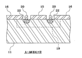
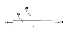
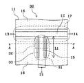
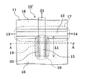
図1に、本発明の高周波スイッチの一実施例の平面図を示す。また図2に、図1のA−A断面拡大図を示す。
【0032】
図1において、高周波スイッチ10は、半導体基板11上に形成されたコプレーナウェーブガイドからなる主線路17とスタブ18を有する。主線路17は主線路電極12およびその幅方向両側に形成されたグランド電極16からなり、一端および他端はそれぞれ端子13および14に接続されている。スタブ18は、スタブ線路電極15およびその幅方向両側に形成されたグランド電極16からなり、一端が主線路17に接続され、他端がグランド電極16に接続されることによって接地されている。より正確に言えば、スタブ18は、そのスタブ線路電極15の一端が主線路17の主線路電極12の側縁に接続され、他端がグランド電極16に接続されている。さらに、スタブ18のスタブ線路電極15の長さは、スタブ18に流れる高周波信号に対して90°の電気長になるように設定されている。
【0033】
半導体基板11には、スタブ18の一端から他端にかけてのスタブ線路電極15とグランド電極16の間において半導体活性層19が形成されている。半導体活性層19はスタブ線路電極15やグランド電極16の下まで延在している。なお、半導体基板11の半導体活性層19が形成されている部分以外は実質的に絶縁体となっている。
【0034】
スタブ18のスタブ線路電極15とグランド電極16の間において、半導体活性層19上にはスタブ線路電極15の長手方向に沿って伸びるゲート電極20が形成されている。ゲート電極20はスタブ線路電極15の他端側からゲート電圧入力端子21に接続されている。ゲート電極20からゲート電圧入力端子21に達するまでの配線にグランド電極16と重なる部分があるが、この領域においては両者は間に絶縁層を介するなどして絶縁されているものとする。ゲート電極20は、図1においては線で表記されているが、実際には図2に示すようにある程度の幅を持った電極である。
【0035】
また、図1および図2においては、主線路電極12は全て半導体基板11上に直接形成されているが、半導体基板11の非活性部分は必ずしも十分な絶縁体とは限らないので、不要なリークを防止するために主線路電極12と半導体基板11との間に絶縁膜を設けることが望ましい。
【0036】
図2のA−A断面拡大図に示すように、半導体活性層19の形成された領域においては、ゲート電極20を挟んで両側に電極が形成されていることから、全体としてFET構造となっていることがわかる。その際、スタブ線路電極15をドレインとすればグランド電極16がソースになる。もちろん逆でも構わない。なお、ゲート電極15と半導体活性層19との接続はショットキ接続にしておき、線路電極15やグランド電極16と半導体活性層19との接続はオーミック接続にしておく必要がある。そして、ゲート電極20の下の半導体活性層19中には空乏層22が形成される。
【0037】
このように構成された高周波スイッチ10において、ドレインとソース(スタブ線路電極15とグランド電極16)の直流電位を例えば0Vにしておき、さらにゲート電極20の直流電位を0Vに設定すると、ゲートがドレインおよびソースに対してバイアスされない状態になって空乏層22が小さくなるためにドレインとソースは半導体活性層19を介してスタブ線路電極15の長手方向全体に渡ってほぼ短絡される。
【0038】
この状態における高周波スイッチ10の等価回路を図3に示す。図3において、Rstはスタブ線路電極15の単位長さあたりの抵抗成分であり、Ronはスタブ線路電極15の単位長さあたりのFET部分のオン抵抗である。RstやRonは小さい値であり、しかも直列及び並列に多数のRstやRonを有するため、高周波スイッチ10は等価的には図4に示すように、主線路電極12がスタブ線路電極15のスタブ線路電極15の付根部分(主線路電極12と接続された位置)で実質的にグランド電極16と短絡されたものとなる。すなわち、主線路17が、その途中で接地された状態になる。
【0039】
この状態においては、高周波スイッチ10を流れる高周波信号は、この接地点でほぼ全反射され一端から他端へ伝搬されなくなる。すなわち、端子13と14の間はオフ状態になる。
【0040】
一方、ドレインとソース(スタブ線路電極15とグランド電極16)の直流電位を例えば0Vにしておき、さらにゲート電極20の直流電位を例えば−3Vに設定すると、ゲートがドレインおよびソースに対して逆バイアス状態になるために空乏層22が大きくなって半導体活性層19が分断され、ドレインとソースは遮断される。
【0041】
この状態における高周波スイッチ10の等価回路を図5に示す。FET部分が遮断されるために、高周波スイッチ10は主線路電極12に単にスタブ線路電極15が接続されただけのものになる。そして、スタブ線路電極15は、流れる高周波信号に対して90°の電気長を有する他端短絡のスタブであるため、主線路電極12との接続点からスタブを見ると理想的には無限大のインピーダンスになる。そのため、高周波スイッチ10は信号周波数においては等価的には図6に示すように主線路電極12のみからなるものとなる。
【0042】
この状態においては、高周波スイッチ10を流れる高周波信号は自由に伝搬できる。すなわち、端子13と14の間はオン状態になる。
【0043】
このように、高周波スイッチ10においては、ゲート電極20に印加する直流電圧によって端子13と端子14の間でスイッチ動作をさせることができる。
【0044】
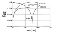
ここで、図7に高周波スイッチ10のオン時およびオフ時における通過特性S21および反射特性S11を示す。図7において、実線が高周波スイッチ10がオンの時の特性で、破線がオフの時の特性である。
【0045】
図7よりわかるように、高周波スイッチ10がオンの時には、高周波信号の周波数である76GHzにおいて通過特性S21は非常に小さくなり、反射特性S11は約−35dBとなって、十分な信号通過特性が得られている。一方、高周波スイッチ10がオフの時には、76GHzにおいて通過特性S21が約−8dB、反射特性S11が約−4dBとなって、ほぼ満足できるな信号遮断特性が得られている。
【0046】
このように構成された高周波スイッチ10においては、FETの一部として利用されているのはスタブ線路電極15だけで、主に高周波信号の流れる主線路電極12はFETの一部にはなっていない。そのため、従来例1ないし3のような、スイッチオン時に高周波信号が半導体活性層からなる抵抗の高い導体を流れるために主線路の挿入損失が増加するという問題は発生しない。
【0047】
また、スタブ線路電極15は主線路電極12に対して直交する方向に伸びるため、従来例2のようなスイッチが主線路の長手方向に大型化するという問題も発生しない。
【0048】
さらに、スタブ線路電極15はFETがオフの時にはショートスタブとして機能するがFETがオンの時にはスタブとしては機能しない。すなわち、FETがオンの時に主線路電極12の一部が接地されるのは、共振によるものではない。そのため、スタブ線路電極15の長さはFETがオフの時に90°の電気長を有するショートスタブとして動作することだけを考えて設定すればよく、FETがオンの時のことは考慮する必要はない。したがって、従来例4のような問題も発生しない。
【0049】
また、主線路電極12の一部の接地に共振を利用しないということは、接地状態が特定の信号周波数でのみ有効であるというような周波数特性を有していないということを意味する。そのため、FETがオンになって高周波スイッチ10がオフになるときには、広い周波数範囲でオフ状態が維持されることになる。すなわち、高いアイソレーション特性が得られる。
【0050】
なお、ここでのアイソレーション特性とは、スイッチオフ時のS21を意味し、これがデシベル表示で大きいほど(絶対値で小さいほど)アイソレーション特性が優れているとみなす。
【0051】
従来例4の場合にはスイッチオフの時に共振によって主線路電極の一部を接地ことよりわかるように特定の周波数に限定して高周波スイッチとして動作するので、この点においても本発明の高周波スイッチ10は優れた性能を備えている。なお、高周波スイッチがオンの時に関しては、本発明も従来例4もともにスタブの共振を利用しているため、性能的な差はない。
【0052】
ところで、図1に示した高周波スイッチ10において、FETがオンの時に主線路電極12をスタブ線路電極15の接続された位置で実質的に接地するためには、スタブ線路電極15の一端から他端にかけての全体にFETが形成されている必要はない。少なくともスタブ線路電極15の一端側、すなわち主線路電極12と接続されている側がある程度の長さに渡ってFETになっていて、FETオン時に十分に低い抵抗値で接地できれば十分である。
【0053】
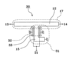
そこで図8に、本発明の高周波スイッチの別の実施例の平面図を示す。図8において、図1と同一もしくは同等の部分には同じ記号を付し、その説明を省略する。なお、FET部分の断面図については図2と同じであるため省略する。
【0054】
図8に示した高周波スイッチ30は、高周波スイッチ10におけるスタブ18に代えてスタブ31を有する。スタブ31において、半導体活性層32はスタブ31の一端側約半分におけるスタブ線路電極15とグランド電極16の間に形成されている。そして、スタブ31のスタブ線路電極15とグランド電極16の間において、半導体活性層32上にはスタブ線路電極15の長手方向に沿って伸びるゲート電極33が半導体活性層32を横切って形成されている。ゲート電極33はゲート電圧入力端子21に接続されている。なお、ゲート電極33は半導体活性層32上だけでなく、スタブ線路電極15とグランド電極16の間の半導体活性層になっていない部分の上にも形成されているが、半導体活性層32上以外に形成された部分はFETとして動作せず単なる信号線路として機能するので、ここではゲート電極とはみなさない。
【0055】
このように構成された高周波スイッチ30においても、FET構造になっている部分は高周波スイッチ10の場合と同じように動作する。そこで、FETをオンにしたときの高周波スイッチ30の等価回路を図9に示す。図9において、図3と同一もしくは同等の部分には同じ記号を付している。
【0056】
図9において、スタブ線路電極15のうちのFETの一部になっていない部分は線路15’として残っているが、主線路電極12と接続されている一端側は高周波スイッチ10の場合と同様に多数の多数のRstやRonを介してグランド電極16と接続された状態になっている。したがって、高周波スイッチ30は高周波スイッチ10と同様に等価的には主線路電極12がスタブ線路電極15の付根部分で実質的に接地されたものとなる。すなわち、主線路17が、その途中で接地された状態になる。
【0057】
そして、この状態においては、高周波スイッチ30を流れる高周波信号は、この接地点でほぼ全反射され一端から他端へ伝搬されなくなる。すなわち、端子13と14の間はオフ状態になる。
【0058】
一方、FETがオフの時には、FET部分が遮断されるために、高周波スイッチ30は主線路電極12に単にスタブ線路電極15が接続されただけのものになる。そして、スタブ線路電極15は、流れる高周波信号に対して90°の電気長を有する他端短絡のスタブであるため、高周波スイッチ30は信号周波数においては等価的には主線路電極12のみからなるものとなる。
【0059】
この状態においては、高周波スイッチ30を流れる高周波信号は自由に伝搬できる。すなわち、端子13と14の間はオン状態になる。
【0060】
なお、ゲート電極の長さ(ゲート幅)は、スタブ線路電極15の一端側においてFETオン時にグランド電極16との十分な短絡状態を実現できる長さであればよい。したがって、高周波スイッチ30のようなスタブ線路電極の長さの半分に限定されるものではなく、半分以下でも半分以上でも構わない。
【0061】
また、FETオフ時には、ドレインとソース間にはオフ容量が分布的に存在する。そのため、スタブ線路電極15とグランド電極16の間の分布容量は、半導体活性層32の存在する部分と存在しない部分で異なる。また、線路電極15の分布的なインダクタンス成分も半導体活性層上に位置するかどうかで厳密には異なる。そのため、スタブ31においては場所によって特性インピーダンスが異なることも考えられる。したがって、スタブ31の長さや幅はこのようなスタブ31の特性インピーダンスの部分的な変化も考慮して決定する必要がある。
【0062】
実際問題として、この場合のスタブは、スタブ線路電極の全長だけでなく、FET部分とそうでない部分とでスタブ線路電極の幅を変えたり、グランド電極との間隔を変えたりして電気長を調整することも十分に考えられる。
【0063】
ところで、高周波スイッチ30においては、高周波スイッチ10に比べてゲート電極の長さであるゲート幅が短い。そのため、FET部分のドレイン・ソース間に形成されるオフ容量も小さくなる。このオフ容量は高周波スイッチ10や30のスイッチング動作の速さを決める時定数に関係する。すなわち、オフ容量が小さいほど時定数が小さくなりスイッチング動作が速くなる。したがって、高周波スイッチ30は高周波スイッチ10に比べて高速なスイッチング動作に対応できるというすぐれたメリットを備えている。
【0064】
また、一般的にゲート電極は直線状に形成されるのが普通で、ゲート電極を折り曲げて形成するのは必ずしも容易ではない。そのため、高周波スイッチ10においては、スタブ18のスタブ線路電極15は直線状に形成せざるを得ない。この場合、高周波スイッチの小型化が難しくなる可能性がある。
【0065】
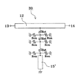
これに対して高周波スイッチ30においては、ゲート電極33はスタブ線路電極15の一端側のみに沿って形成されていればよい。そのため、図10に概略図で示すように、スタブ線路電極15におけるゲート電極33の形成されていない他端側を折り曲げることが可能になる。そして、これによって高周波スイッチの小型化が可能になる。
【0066】
このように、高周波スイッチ30においては、高周波スイッチ10と比較して、より高速なスイッチング動作ができ、またスタブを折り曲げることができるためにさらなる小型化を図ることができるというメリットを備えている。
【0067】
なお、高周波スイッチ10や高周波スイッチ30においては、スタブ線路電極の両側にFET構造を形成しているが、片側のみに形成しても構わない。この場合はFETオン時の抵抗値が少し大きくなるが、この点を除けば上述の実施例とほぼ同様の作用効果を奏することができる。
【0068】
また、高周波スイッチ10や高周波スイッチ30においては、主線路やスタブが対称形のコプレーナウェーブガイドであるとして、スタブにおいては対称形のコプレーナウェーブガイドのためのグランド電極をFETのソース電極として利用していた。しかしながら、主線路やスタブは対称形のコプレーナウェーブガイドに限られるものではなく、例えばグランド電極が片側にしかない非対称型のコプレーナウェーブガイドでもよい。あるいは、マイクロストリップ線路などの線路電極に沿ったグランド電極を備えていない他の伝送線路であっても構わない。但し、その場合にはスタブ線路電極に隣接してグランド電極を別途設ける必要がある。また、それと同時に、隣接して形成されるグランド電極によってスタブの特性インピーダンスが理想的なマイクロストリップ線路の場合に比べて変化するため、スタブ線路電極の長さを決める際には、その点を考慮する必要がある。但し、これらの点を除けば、高周波スイッチとしては上述の実施例とほぼ同様の作用効果を得ることができる。
【0069】
以下、上述のFET構造が形成されたスタブを利用した高周波スイッチの他の実施例について説明する。なお、以下の実施例においては、高周波スイッチ30におけるスタブ構造を採用するが、もちろん高周波スイッチ10におけるスタブ構造でも構わないものである。
【0070】
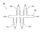
まず、図11に、本発明の高周波スイッチのさらに別の実施例の概略図を示す。図11は特徴部分のみを示すために簡略化した図で、図1と同一もしくは同等の部分には同じ記号を付し、その説明を省略する。
【0071】
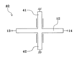
図11に示した高周波スイッチ40において、41、42はFET構造が形成されたスタブのスタブ線路電極を意味している。線路の両側の線はゲート線路を意味している。なお、グランド電極やゲート電圧入力端子については記載を省略している。
【0072】
図11に示すように、高周波スイッチ40においては、2つのスタブ線路電極41、42が、主線路電極12の側縁に幅方向両側から互いに対向して設けられている。このように構成された高周波スイッチ40において、スタブ線路電極41、42を含むスタブは、それぞれ高周波スイッチ30におけるスタブ31と同じ機能を果たす。
【0073】
そのため、高周波スイッチ40のオン・オフに対応して2つのスタブのFETを同時にオフ・オンさせることによって、高周波スイッチオフ時に主線路電極12をその途中で接地した状態にすることができる。しかも、高周波スイッチ30の場合は主線路電極12の所定の位置の片側の側縁だけが接地されたのに対して、高周波スイッチ40においては主線路電極12の所定の位置の両側の側縁が同時に接地される。これは、その点が高周波スイッチ30の場合に比べて半分の抵抗値を介して接地されることを意味し、高周波スイッチ40のオフ時の遮断状態をより完全なものにできることを意味する。すなわち、アイソレーション特性をさらに向上させることができる。
【0074】
また、見方を変えれば、もしも接地抵抗が同じで構わないのであれば、各スタブのゲート電極の長さ(ゲート幅)をより短くできることを意味する。ゲート幅を短くできるということは、上述のようにスイッチング動作をさらに高速化できることを意味する。また、スタブ線路電極41、42の中のゲート電極が形成されているために直線状でなければならない部分が短くなり、スタブ形状の自由度が増し、高周波スイッチのさらなる小型化を図れることを意味する。
【0075】
このように、高周波スイッチ40においては、オフ時の高周波信号の遮断性能をさらに向上させることができ、あるいはスイッチング動作を高速化させたり小型化を図ったりすることができる。
【0076】
また、図12に、本発明の高周波スイッチのさらに別の実施例の概略図を示す。図12は特徴部分のみを示すために簡略化した図で、図1と同一もしくは同等の部分には同じ記号を付し、その説明を省略する。
【0077】
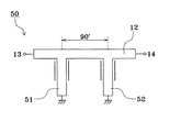
図12に示した高周波スイッチ50において、51、52はFET構造が形成されたスタブのスタブ線路電極を意味している。線路の両側の線はゲート線路を意味している。なお、グランド電極やゲート電圧入力端子については記載を省略している。
【0078】
図12に示すように、高周波スイッチ50においては、2つのスタブ線路電極51、52が、主線路電極12の片側の側縁の、主線路電極12の長手方向に電気長で90°離れた位置に接続して設けられている。このように構成された高周波スイッチ50において、スタブ線路電極51、52を含むスタブは、それぞれ高周波スイッチ30におけるスタブ31と同じ機能を果たす。
【0079】
そのため、高周波スイッチ50のオン・オフに対応して2つのスタブのFETを同時にオフ・オンさせることによって、高周波スイッチオフ時に主線路電極12をその途中の2カ所で接地した状態にすることができる。このように2カ所を接地することによって、各スタブのゲート電極の長さが短くて1カ所の接地では必ずしも十分ではないような場合でも、より完全に高周波信号を反射させて高周波スイッチ50を遮断させることができる。しかも、2つのスタブが主線路電極12の長手方向に電気長で90°離れた位置に接続して設けられているため、一方のスタブから見た他方のスタブのインピーダンスは無限大となり、実質的には見えなくなるため、一方のスタブでの反射信号が他方のスタブの特性、特に接地状態に悪影響を与えることがない。
【0080】
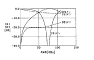
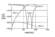
ここで、図13に、高周波スイッチ50のオン時およびオフ時における通過特性S21および反射特性S11を示す。図13において、実線が高周波スイッチ50がオンの時の特性で、破線がオフの時の特性である。
【0081】
図13よりわかるように、高周波スイッチ50がオンの時には、高周波信号の周波数である76GHzにおいて通過特性S21は損失が非常に小さくなって0dBに近くなり、反射特性S11は−40dB以下となって、十分な信号通過特性が得られている。一方、高周波スイッチ50がオフの時には、76GHzにおいて通過特性S21が約−19dB、反射特性S11が約−4dBとなって、高周波スイッチ10に比べて通過量がさらに少なくなり、十分な信号遮断特性が得られている。
【0082】
このように、高周波スイッチ50においては、スイッチオフ時の遮断特性をさらに向上させることができる。
【0083】
なお、高周波スイッチ50においてはFET構造が形成されたスタブを2つ用いているが、各スタブが主線路電極12の長手方向に電気長で90°ずつ離れた位置に接続して設けられるのであれば、スタブの数は3つ以上でも構わないものである。
【0084】
また、高周波スイッチ50においては、各スタブは主線路電極12の片側の側縁のみに接続して設けられているが、それぞれどちら側の側縁に接続して設けられていても構わないものである。
【0085】
ところで、高周波スイッチ50においては、相互の影響を避けるために2つのスタブを主線路電極12の長手方向に電気長で90°離れた位置に接続して設けるとしたが、各スタブをさらに近接して設けたものも考えられる。
【0086】
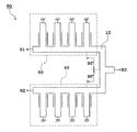
そこで、図14に、本発明の高周波スイッチのさらに別の実施例の概略図を示す。図14も特徴部分のみを示すために簡略化した図で、図1と同一もしくは同等の部分には同じ記号を付し、その説明を省略する。
【0087】
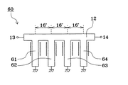
図14に示した高周波スイッチ60において、61、62、63、64はいずれもFET構造が形成されたスタブのスタブ線路電極を意味している。線路の両側の線はゲート線路を意味している。なお、グランド電極やゲート電圧入力端子については記載を省略している。
【0088】
図14に示すように、高周波スイッチ60においては、4つのスタブ線路電極61、62、63、64が、主線路電極12の片側の側縁の、それぞれ主線路電極12の長手方向に電気長で16°離れた位置に接続して設けられている。各スタブ線路電極の長さは、信号周波数において電気長で110°に設定されている。また、主線路の特性インピーダンスは75Ωに、スタブの特性インピーダンスは35Ωに設定されている。このように構成された高周波スイッチ60において、スタブ線路電極61、62、63、64を含むスタブは、それぞれ高周波スイッチ30におけるスタブ31と同じ機能を果たす。
【0089】
高周波スイッチ60においても、そのオン・オフに対応して4つのスタブのFETを同時にオフ・オンさせることによって、高周波スイッチオフ時に主線路電極12をその途中の4カ所で接地した状態にすることができる。このように4カ所を接地することによって、2カ所の場合よりもさらに接地状態を十分なものにして、より完全に高周波信号を反射させて高周波スイッチ60を遮断させることができる。
【0090】
なお、高周波スイッチ60においては、主線路電極12の長手方向に関する各スタブの間隔が16°となっている。そのため、各スタブが相互に見えなくなって相互の悪影響を避けられるというメリットはない。しかしながら、逆に、FETオフ(スイッチオン)時における反射特性において周波数帯域が広がって他の周波数でも整合が取れるようになるというメリットがある。また、スタブの間隔が短いために高周波スイッチの長手方向のサイズを小さくすることができる。さらに、主線路の長さが短くなるためにスイッチオン時の挿入損失の低減を図ることができる。
【0091】
また、スタブの数が多いために、FETオン時における、各スタブ間での高周波信号の反射と各スタブの接地抵抗とによって、各スタブにおける電力消費が増えてスイッチオフ時の挿入損失が大きくなるというメリットがある。
【0092】
ここで、図15に、高周波スイッチ60のオン時およびオフ時における通過特性S21および反射特性S11を示す。図15において、実線が高周波スイッチ60がオンの時の特性で、破線がオフの時の特性である。
【0093】
図15よりわかるように、高周波スイッチ60がオンの時には、高周波信号の周波数である76GHzにおいて通過特性S21は損失が非常に小さくなって0dBに近くなり、反射特性S11は広い帯域で−15dB以下となって、十分な信号通過特性が得られている。一方、高周波スイッチ60がオフの時には、76GHzにおいて通過特性S21が約−33dB、反射特性S11が約−3dBとなって、高周波スイッチ10に比べて通過量が大幅に少なくなり、十分な信号遮断特性が得られていることがわかる。
【0094】
なお、スイッチオン時の反射特性S11において谷が2つ存在するのはスタブの数を多くしているからである。この谷の周波数、間隔、谷と谷の間の反射量などの特性は、スタブ間隔、スタブの長さや特性インピーダンス、主線路の特性インピーダンスを適宜調整することによって設定できる。高周波スイッチ60においてスタブ長さを電気長で110°に設定したのはこのためである。
【0095】
このように、高周波スイッチ60においては、オフ時の遮断特性をさらに向上させることができる。
【0096】
なお、高周波スイッチ60においては、スタブ間の間隔を16°としているが、これは1つの例であって、必要に応じて自由に設定して構わない。また、スタブの数についても2つ以上であれば自由に設定して構わない。
【0097】
さらに、高周波スイッチ60においては、主線路電極12の片側側縁のみにスタブを接続しているが、例えば図16に示す高周波スイッチ70のように両側側縁にスタブを接続しても構わない。特に、高周波スイッチ70のように交互にスタブを接続する場合には、片側側縁のみにスタブを接続する場合に比べてスタブ間の間隔をさらに狭くすることができ、高周波スイッチのさらなる小型化を図ることも可能になる。
【0098】
上記の各実施例においては、2つの端子間を導通させたり遮断したりするいわゆるSPST(Single Pole Single Through、1対1)スイッチの例について説明してきたが、本発明の高周波スイッチを複数個用いれば、いわゆるSPxT(Single Pole x Through、1対多)スイッチを構成することもできる。
【0099】
図17に、本発明の高周波スイッチのさらに別の実施例の概略図を示す。図17は特徴部分のみを示すために簡略化した図で、図1と同一もしくは同等の部分には同じ記号を付し、その説明を省略する。
【0100】
図17に示した高周波スイッチ80においては、図14に示した高周波スイッチ60を2つ用いて、その一端同士を接続して3番目の端子としたものである。図17において、一方の高周波スイッチ60の一端は端子81に接続され、他方のの高周波スイッチ60の一端は端子82に接続され、2つの高周波スイッチ60の他端同士は互いに接続されるとともに端子83に接続されている。そして、その接続点から各高周波スイッチ60における最も近いスタブ線路電極の接続点までの主線路電極12の長さを、高周波信号に対する電気長が略90°になるように設定している。
【0101】
このように構成された高周波スイッチ80においては、各高周波スイッチ60がそれぞれ低損失なスイッチとして動作する。しかも、接続点から各高周波スイッチ60における最も近いスタブ線路電極の接続点までの主線路電極12の長さを、高周波信号に対する電気長が略90°になるように設定しているために、一方の高周波スイッチ60がオンで他方の高周波スイッチ60がオフの時に、オフ状態の高周波スイッチ60が主線路電極12に対して無限大のインピーダンスを持つように見える。すなわち、オフ状態の高周波スイッチ60が存在しないのと同じことになる。そのため、不整合やスイッチオン時の挿入損失の少ないSPDT(Single Pole Dual Through、1対2)スイッチが実現できる。
【0102】
なお、上記の実施例においては2つの高周波スイッチ60の他端同士の接続点から各高周波スイッチ60における最も近いスタブ線路電極の接続点までの主線路電極12の長さを、高周波信号に対する電気長が略90°になるように設定したが、これは各スタブのFETがオンの時のグランドとの間の抵抗値が十分に小さい理想的な状態の場合である。実際にはこの部分の線路電極12の長さが電気長で約80°になることも考えられる。
【0103】
なお、高周波スイッチ80においてはSPDTスイッチを実現しているが、例えば3つ以上の高周波スイッチ60を用いて同様な方法でSPxTスイッチを構成することも可能である。
【0104】
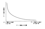
ところで、上記の各実施例は図1に示した高周波スイッチ10の構造を基本構造としている。そして、高周波スイッチ10においては、スイッチをオフする場合、すなわちFET部分をオンする場合には、ゲートの直流電位をドレインやソースと同じ0Vにしてゲートがドレインおよびソースに対してバイアスされない状態にするとしている。しかしながら、ゲートをバイアスしない状態においても空乏層は存在する。そこで、ゲートをドレインやソースに対して順バイアスにすることによって空乏層をさらに小さくすることが考えられる。
【0105】
ゲートをドレインやソースに対して順バイアスにするとゲート電流が流れる。ゲート幅が長い場合、ゲート電極には抵抗が存在するためにゲート電圧入力端子に近い位置と遠い位置では電位差が生じる。その結果、図18に示すように、ゲート電圧入力端子に近いほどドレインやソースとの電位差が大きくなって流れるゲート順方向電流も多くなるという傾向が生じる。ゲート順方向電流が多い部分ほど空乏層は小さく、そのためドレインとソースの間の抵抗もより小さい。これを高周波スイッチ10に当てはめれば、スタブ線路電極15の単位長さあたりのFET部分のオン抵抗Ronは、スタブ線路電極15の一端側(主線路電極12と接続されている側)の方が大きく、他端側の方が小さくなる。これは、少なくともスタブ線路電極15の一端側を十分に低い抵抗値で接地できればよいという本発明のポイントから見れば必ずしも理想的とは言えない。
【0106】
そこで、図19に、この点を改善した本発明の高周波スイッチのさらに別の実施例の平面図を示す。図19において、図1と同一もしくは同等の部分には同じ記号を付し、その説明を省略する。なお、FET部分の断面図についても図2と同じであるため省略する。
【0107】
図19に示した高周波スイッチ10’において、高周波スイッチ10との違いは、ゲート電極20がスタブ線路電極15の一端側から引き出されてゲート電圧入力端子21に接続されている点だけである。このゲート電極引き出し構成において、ゲート電極20からゲート電圧入力端子21に達するまでの配線に主線路電極12およびグランド電極16と重なる部分があるが、この領域においてはエアーブリッジ構造で一方が他方を跨いでいたり、間に絶縁層を介するなどして両者は絶縁されているものとする。
【0108】
このように構成された高周波スイッチ10’において、ドレインとソース(スタブ線路電極15とグランド電極16)の直流電位を例えば0Vにしておき、さらにゲート電極20の直流電位を例えば+1Vに設定すると、ゲートがドレインおよびソースに対して順バイアス状態になって空乏層22が小さくなるためにドレインとソースは半導体活性層19を介してスタブ線路電極15の長手方向全体に渡ってほぼ短絡される。
【0109】
しかも、ゲートをドレインおよびソースに対して順バイアス状態にする場合には、上述のようにゲート電圧入力端子に近いほど単位長さあたりのFET部分のオン抵抗Ronが小さくなるので、高周波スイッチ10’においてはスタブ線路電極15の一端側ほど良好な短絡状態が得られる。その結果、高周波スイッチ10’においては高周波スイッチ10の場合よりも良好なオフ状態を実現することができる。なお、スイッチのオン状態においては、ゲートをドレインおよびソースに対して逆バイアス状態にするので高周波スイッチ10と10’で特性的な違いはない。
【0110】
このように、高周波スイッチ10’の構成を採用すると、スイッチオフ時の遮断特性を向上させることができる。そして、この構成はスタブ線路電極の一端側の短絡状態を良くするものであるため、図8に示した高周波スイッチ30の場合でも同様に適用することができ、同様の効果を得ることができる。
【0111】
また、このゲート電極引き出し構成を採用することによって1つのスタブ線路電極あたりのスイッチオフ時の遮断特性を向上させることができるため、複数のスタブ線路電極を用いるスイッチにおいても特性を向上させることができる。すなわち、例えば図14に示した高周波スイッチ60に高周波スイッチ10’のゲート電極引き出し構成を採用する場合、より少ないスタブ線路電極の数で同等のアイソレーション特性が得られるようになる。そして、スタブ線路電極の数を少なくできるということは、その分だけ高周波スイッチの面積を小さくできることを意味する。また、スタブ線路電極の数を少なくできるということは、その分だけスイッチオン時の挿入損失を小さくできることも意味する。そして、この効果は高周波スイッチ10や60のようなSPSTスイッチに限られるものではなく、図17に示す高周波スイッチ80のようなSPDTスイッチを含むSPxTスイッチにおいても同様に得ることができるものである。
【0112】
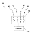
最後に、図20に、本発明の電子装置の一実施例のブロック図を示す。図20において、電子装置90はレーダー装置で、送受信回路91、本発明の高周波スイッチ92、および4つのアンテナ93、94、95、96から構成されている。このうち、高周波スイッチ92は、4つの高周波スイッチを内蔵した1入力4出力の高周波スイッチで、各内蔵スイッチは1つずつ順にオン状態になり、オン状態の内蔵スイッチを介して送受信回路91といずれかのアンテナが接続され、信号の送信および受信がなされる。4つのアンテナ93、94、95、96はいずれもその指向方向が異なっており、高周波スイッチ92の内蔵スイッチを切り換えることによって4つの方向に関するレーダーとして動作させることができる。
【0113】
このように構成された電子装置90においては、本発明の高周波スイッチ92を用いているために、スイッチオン時の挿入損失が少ないために信号の損失を少なくして低消費電力化を図ることができる。また、スイッチオフ時の遮断特性に優れているために、異なる方向にレーダー波を放射したり異なる方向の物体を検知するといった誤動作も少なくなる。
【0114】
なお、図20においては電子装置としてレーダー装置を示したが、本発明の高周波スイッチを用いたものであればどのような電子装置であっても構わないものである。
【0115】
【発明の効果】
本発明の高周波スイッチにおいては、2つの端子間に設けられた主線路電極と、一端が主線路電極の側縁に接続されるとともに他端が接地されたスタブ線路電極と、スタブ線路電極の幅方向に隣接して設けられたグランド電極とを備え、スタブ線路電極の少なくとも一端側の側縁とグランド電極の間の基板部分に、スタブ線路電極およびグランド電極の下まで延在する半導体活性層が形成されるとともに、スタブ線路電極およびグランド電極の間の半導体活性層上にスタブ線路電極の長手方向に沿って伸びるゲート電極が設けられることによってFET構造が形成される。
【0116】
そして、このFETをオンすることによって主線路電極の一部を接地して主線路電極を流れる高周波信号を遮断し、FETをオフすることによって主線路電極に流れる高周波信号を導通させるスイッチとして動作させることができる。
【0117】
しかも、本発明の高周波スイッチにおいては、主線路電極をFETの一部にしていないために、スイッチオン時の挿入損失を低くすることができる。また、周波数特性のない接地状態が実現されるため、スイッチオフ時に安定して高周波信号を遮断することができる。その結果、高いアイソレーション特性を得ることができる。
【0118】
また、本発明の電子装置によれば、本発明の高周波スイッチを用いることによって、低消費電流化と誤動作の低減を図ることができる。
【図面の簡単な説明】
【図1】本発明の高周波スイッチの一実施例を示す平面図である。
【図2】図1の高周波スイッチのA−A断面拡大図である。
【図3】図1の高周波スイッチのオフ時の等価回路図である。
【図4】図1の高周波スイッチのオフ時の実質的な等価回路図である。
【図5】図1の高周波スイッチのオン時の等価回路図である。
【図6】図1の高周波スイッチのオン時の実質的な等価回路図である。
【図7】図1の高周波スイッチのスイッチ特性を示す特性図である。
【図8】本発明の高周波スイッチの別の実施例を示す平面図である。
【図9】図8の高周波スイッチのオフ時の実質的な等価回路図である。
【図10】図8の高周波スイッチのバリエーションを示す平面図である。
【図11】本発明の高周波スイッチのさらに別の実施例を示す平面図である。
【図12】本発明の高周波スイッチのさらに別の実施例を示す平面図である。
【図13】図12の高周波スイッチのスイッチ特性を示す特性図である。
【図14】本発明の高周波スイッチのさらに別の実施例を示す平面図である。
【図15】図14の高周波スイッチのスイッチ特性を示す特性図である。
【図16】本発明の高周波スイッチのさらに別の実施例を示す平面図である。
【図17】本発明の高周波スイッチのさらに別の実施例を示す平面図である。
【図18】ゲート電極上の位置とゲート順方向電流の関係を示す特性図である。
【図19】本発明の高周波スイッチのさらに別の実施例を示す平面図である。
【図20】本発明の電子装置の一実施例を示すブロック図である。
【符号の説明】
10、30、40、50、60、70、80、10’…高周波スイッチ
11…半導体基板
12…主線路電極
13、14、81、82、83…端子
15、41、42、51、52、61、62、63、64、71、72、73、74…スタブ線路電極
16…グランド電極
17…主線路
18、31…スタブ
19、32…半導体活性層
20、33…ゲート電極
21…ゲート電圧入力端子
22…空乏層
90…電子装置[0001]
TECHNICAL FIELD OF THE INVENTION
The present invention relates to a high-frequency switch and an electronic device using the same, and particularly to a high-frequency switch used for switching a signal in a millimeter wave band and an electronic device using the same.
[0002]
[Prior art]
A switch using a PIN diode is generally used as a switch used for switching signals in the millimeter wave band, but a switch using an FET may be used at a relatively low frequency. Among them, there is a switch that uses a line itself through which a high-frequency signal passes as a drain and a source of an FET, and specific examples are disclosed in
[0003]
Patent Document 1 (Conventional Example 1) discloses that a signal line is divided into a plurality of drain electrodes by a plurality of slits crossing in the width direction, and the source electrode and the gate also extend in the width direction of the signal line in the slits. A high-frequency switch using a part of a signal line as an FET by forming an electrode for use (line) is disclosed (for example, FIG. 13). The drain electrodes are connected by metal wiring. An inductance element that resonates in parallel with the off-capacitance of the FET at the signal frequency is connected between the drain and the source of the FET.
[0004]
In the first conventional example, the signal line itself is always conductive in terms of direct current including the portion where the FET is formed. Then, when the FET is turned on, the impedance of the circuit connected between the signal line and the ground is reduced, and the circuit is almost short-circuited. As a result, a part of the signal line is set to a substantially ground state, and the high-frequency signal is reflected and the conduction is blocked. Conversely, when the FET is off, the impedance at the frequency of the high-frequency signal of the circuit connected between the signal line and the ground becomes infinite due to the parallel resonance of the off capacitance of the FET and the inductance element. This means that nothing is connected to the signal line at the frequency of the high-frequency signal, so that the high-frequency signal conducts. The switching operation is performed in this manner.
[0005]
In Patent Document 2 (conventional example 2), a ground electrode (functioning as a source electrode) is formed adjacent to a part of a signal line (functioning as a drain electrode) along the longitudinal direction thereof, and a gap between the two is formed. Discloses a high-frequency switch in which a gate electrode extending along the longitudinal direction of a signal line is formed (for example, FIG. 6).
[0006]
In the second conventional example, when the FET is off, a part of the signal line operating as the drain operates as a mere signal line, so that the high-frequency signal conducts through the signal line. On the other hand, when the FET is on, a part of the signal line operating as a drain is connected to the ground electrode, so that a part of the signal line is substantially grounded, and the high-frequency signal is reflected. , Conduction is blocked.
[0007]
Patent Literature 3 (Conventional Example 3) discloses an FET configuration similar to that of Conventional Example 1 (FIG. 8, there is no inductance element for parallel resonance), and a drain, source, and gate of an FET having a signal line with the same configuration. A configuration configured to extend in the direction (FIG. 1) is disclosed.
[0008]
In the third conventional example, the same operation as the second conventional example is performed in that a part of the signal line is substantially grounded when the FET is turned on to block a high-frequency signal.
[0009]
Patent Document 4 (Conventional Example 4) discloses an FET in which a stub of 1/4 wavelength is connected to a main line of a signal line, and a tip of the stub is used as a drain electrode and a source electrode is grounded to form an FET. (FIGS. 2 and 6) are disclosed. By turning on and off the FET, the stub is operated as a short stub or an open stub of 1/4 wavelength.
[0010]
Also in Conventional Example 4, the stub becomes an open stub having a quarter wavelength when the FET is turned off, and a part of the signal line is substantially grounded at the frequency of the high-frequency signal to block the high-frequency signal. The same operation as in the conventional examples 2 and 3 is performed.
[0011]
[Patent Document 1]
JP-A-6-232601
[Patent Document 2]
JP-A-10-41404
[Patent Document 3]
JP 2000-294568 A
[Patent Document 4]
JP 2000-332502 A
[0012]
[Problems to be solved by the invention]
By the way, in the conventional example 1, it is necessary to reduce the conduction resistance when the FET is turned on. To that end, it is necessary to increase the number of gate lines and the number of gate electrodes to increase the total gate width of the FET. There is. Increasing the total gate width necessarily increases the off-capacitance of the FET. Accordingly, it is necessary to reduce the inductance value of the inductance element for parallel resonance. However, there is a limit to reducing the shape of the inductance element while maintaining the accuracy of the inductance value. Since the inductance value needs to be reduced as the signal frequency increases, this configuration has a problem that it becomes difficult to use as the signal frequency increases.
[0013]
On the other hand, in the second conventional example, since the resonance phenomenon is not used, there is no problem that the use becomes difficult when the signal frequency increases as described above. However, in the conventional example 1, the main line through which the high-frequency signal flows when the switch is turned on in the signal line itself is the drain electrode of the FET. Since the drain electrode is at least partially formed on the semiconductor active layer, this means that a part of the main line is formed on the semiconductor active layer. A high-frequency signal also flows through the semiconductor active layer as a part of the line, but since the semiconductor active layer is a conductor having a higher resistance than the drain electrode, this means that the resistance of the main line increases. Therefore, in the switch in which the main line itself is the drain electrode of the FET as in the conventional example 1, there is also a problem that this causes an increase in the insertion loss of the main line.
[0014]
Further, the on-resistance per unit length of the FET (per unit gate width) can be reduced by changing the cross-sectional structure of the FET, but this is not always easy. When the on-resistance per unit length cannot be changed, it is necessary to increase the gate width of the FET in order to sufficiently ground the main line when the FET is on. Increasing the gate width of the FET means extending the gate electrode in the longitudinal direction of the signal line, which also means increasing the drain electrode. This means that the switch becomes larger in the longitudinal direction of the main line. Since the drain electrode is also a main line through which a high-frequency signal formed on the semiconductor active layer flows, the tendency to increase the insertion loss of the main line as described above is further strengthened.
[0015]
Next, Conventional Example 3 has the same basic configuration as Conventional Example 1, and has the same problem.
[0016]
Finally, in the conventional example 4, since the main line through which the high-frequency signal flows is not a drain electrode, there is no problem that the insertion loss at the time of switch-on increases. However, in order to ground the end of the stub with a sufficiently low resistance value, it is necessary to increase the gate width of the FET. When the gate width of the FET is increased, the capacitance between the drain and the source when the FET is off increases. This means that a large capacitance exists between the tip of the open stub and the ground when the FET is off. If there is a large capacitance at the tip of the open stub, the resonance frequency of the open stub decreases, so that it is highly likely that the resonance frequency differs from that of the short stub. The inability of the open stub and the short stub to have the same resonance frequency means that they do not function properly as a switch, which is a serious problem.
[0017]
An object of the present invention is to solve the above-described problems, and a high-frequency switch that can be used at a high frequency, has a low insertion loss at the time of switch-on, and has a high signal blocking performance at the time of switch-off, and uses the same. Provide an electronic device.
[0018]
[Means for Solving the Problems]
In order to achieve the above object, a high-frequency switch according to the present invention includes a main line electrode provided between two terminals, a stub line having one end connected to a side edge of the main line electrode and the other end grounded. An electrode, and a ground electrode provided adjacent to the stub line electrode in the width direction,
A semiconductor active layer extending below the stub line electrode and the ground electrode is formed on a substrate portion between at least one side edge of the stub line electrode and the ground electrode, and the stub line electrode and An FET structure is formed by providing a gate electrode extending along the longitudinal direction of the stub line electrode on the semiconductor active layer between the ground electrodes.
[0019]
Further, a semiconductor active layer extending below the stub line electrode and the ground electrode is formed on a substrate portion between a side edge from one end side to the other end side of the stub line electrode and the ground electrode. In addition, an FET structure is formed by providing a gate electrode extending along the longitudinal direction of the stub line electrode on the semiconductor active layer between the stub line electrode and the ground electrode.
[0020]
Further, the FET structure is formed on both side edges of the stub line electrode.
[0021]
Further, the stub line electrode on which the FET structure is formed forms a coplanar waveguide together with the ground electrode.
[0022]
The stub line electrode on which the FET structure is formed is formed so as to have an electrical length of about 90 ° with respect to a flowing high-frequency signal.
[0023]
In the high frequency switch according to the present invention, one end of the stub line electrode having the plurality of FET structures is connected to a side edge of the main line electrode.
[0024]
One end of each of the stub line electrodes on which the two FET structures are formed is connected so as to face each other from both sides in the width direction of the main line electrode.
[0025]
Alternatively, one end of the stub line electrode on which the plurality of FET structures are formed is connected to the side edge of the main line electrode at a predetermined interval in the longitudinal direction. Further, one ends of the stub line electrodes on which the plurality of FET structures are formed are connected to the main line electrode side edges at an electrical length of approximately 90 ° with respect to a high-frequency signal flowing in the longitudinal direction. It is characterized by having.
[0026]
Further, a high-frequency switch according to the present invention includes a plurality of the high-frequency switches described above, and one end of each of the plurality of high-frequency switches has an electrical length of a high-frequency signal to a connection point of a stub line electrode formed with the FET structure. It is characterized in that they are connected to each other through a 90 ° main line electrode.
[0027]
Further, in the high frequency switch according to the present invention, the gate electrode is drawn out from one end of the stub line electrode.
[0028]
Further, an electronic device of the present invention is characterized by using the above high-frequency switch.
[0029]
With such a configuration, the high-frequency switch of the present invention can use a high frequency, have a low insertion loss when the switch is turned on, and has a high signal blocking performance when the switch is turned off.
[0030]
Further, in the electronic device of the present invention, low power consumption and malfunction can be reduced.
[0031]
BEST MODE FOR CARRYING OUT THE INVENTION
FIG. 1 shows a plan view of one embodiment of the high-frequency switch of the present invention. FIG. 2 is an enlarged cross-sectional view taken along line AA of FIG.
[0032]
In FIG. 1, the high-
[0033]
A semiconductor
[0034]
Between the
[0035]
Also, in FIGS. 1 and 2, the
[0036]
As shown in the AA cross-sectional enlarged view of FIG. 2, in the region where the semiconductor
[0037]
When the DC potential of the drain and the source (the
[0038]
FIG. 3 shows an equivalent circuit of the high-
[0039]
In this state, the high-frequency signal flowing through the high-
[0040]
On the other hand, when the DC potential of the drain and the source (
[0041]
FIG. 5 shows an equivalent circuit of the high-
[0042]
In this state, the high-frequency signal flowing through the high-
[0043]
As described above, in the high-
[0044]
Here, FIG. 7 shows a transmission characteristic S21 and a reflection characteristic S11 when the high-
[0045]
As can be seen from FIG. 7, when the high-
[0046]
In the high-
[0047]
Further, since the
[0048]
Further, the
[0049]
Further, not using resonance for grounding a part of the
[0050]
Here, the isolation characteristic means S21 at the time of switch-off, and it is considered that the larger this is in decibel display (the smaller the absolute value is), the better the isolation characteristic is.
[0051]
In the case of the prior art example 4, when the switch is turned off, a part of the main line electrode is limited to a specific frequency and operates as a high-frequency switch as can be seen from grounding by resonance. Has excellent performance. When the high-frequency switch is on, there is no difference in performance because both the present invention and Conventional Example 4 use the resonance of the stub.
[0052]
By the way, in the high-
[0053]
FIG. 8 shows a plan view of another embodiment of the high-frequency switch of the present invention. 8, the same or equivalent parts as those in FIG. 1 are denoted by the same reference numerals, and description thereof will be omitted. Note that the sectional view of the FET portion is the same as that of FIG.
[0054]
The high-
[0055]
Also in the high-
[0056]
In FIG. 9, a portion of the
[0057]
Then, in this state, the high-frequency signal flowing through the high-
[0058]
On the other hand, when the FET is off, the high-
[0059]
In this state, the high-frequency signal flowing through the high-
[0060]
The length (gate width) of the gate electrode may be any length at one end of the
[0061]
When the FET is off, off capacitance is distributed between the drain and the source. Therefore, the distributed capacitance between the
[0062]
As a practical matter, the stub in this case adjusts not only the entire length of the stub line electrode, but also the electric length by changing the width of the stub line electrode between the FET part and the other part, and changing the distance from the ground electrode. It is quite possible to do it.
[0063]
Incidentally, in the high-
[0064]
Generally, the gate electrode is generally formed in a straight line, and it is not always easy to bend the gate electrode. Therefore, in the
[0065]
On the other hand, in the high-
[0066]
As described above, the high-
[0067]
In the
[0068]
In the high-
[0069]
Hereinafter, another embodiment of the high-frequency switch using the stub having the above-described FET structure will be described. In the following embodiment, the stub structure in the high-
[0070]
First, FIG. 11 shows a schematic diagram of still another embodiment of the high-frequency switch of the present invention. FIG. 11 is a simplified view showing only the characteristic portions. The same or equivalent portions as those in FIG. 1 are denoted by the same reference numerals, and description thereof will be omitted.
[0071]
In the
[0072]
As shown in FIG. 11, in the high-
[0073]
Therefore, by turning off and on the FETs of the two stubs at the same time in response to the on / off of the
[0074]
In other words, if the ground resistance is the same, it means that the length (gate width) of the gate electrode of each stub can be reduced. The fact that the gate width can be shortened means that the switching operation can be further accelerated as described above. In addition, since the gate electrodes in the
[0075]
As described above, the high-
[0076]
FIG. 12 is a schematic view of a high-frequency switch according to still another embodiment of the present invention. FIG. 12 is a simplified view showing only the characteristic portions. The same or equivalent portions as those in FIG. 1 are denoted by the same reference numerals, and description thereof will be omitted.
[0077]
In the high-
[0078]
As shown in FIG. 12, in the high-
[0079]
Therefore, by turning off and on the FETs of the two stubs at the same time in response to the on / off of the high-
[0080]
Here, FIG. 13 shows a transmission characteristic S21 and a reflection characteristic S11 when the high-
[0081]
As can be seen from FIG. 13, when the high-
[0082]
Thus, in the high-
[0083]
In the high-
[0084]
In the high-
[0085]
In the high-
[0086]
Therefore, FIG. 14 is a schematic diagram of still another embodiment of the high-frequency switch of the present invention. FIG. 14 is also a simplified diagram showing only the characteristic portions, and the same or equivalent portions as those in FIG. 1 are denoted by the same reference numerals and description thereof is omitted.
[0087]
In the high-
[0088]
As shown in FIG. 14, in the high-
[0089]
Also in the high-
[0090]
In the high-
[0091]
Further, since the number of stubs is large, the power consumption in each stub increases due to the reflection of the high-frequency signal between the stubs and the ground resistance of each stub when the FET is on, and the insertion loss when the switch is off increases. There is a merit.
[0092]
Here, FIG. 15 shows the pass characteristics S21 and the reflection characteristics S11 when the high-
[0093]
As can be seen from FIG. 15, when the high-
[0094]
The reason why there are two valleys in the reflection characteristic S11 when the switch is on is because the number of stubs is increased. Characteristics such as the frequency of the valley, the interval, and the amount of reflection between the valleys can be set by appropriately adjusting the stub interval, the stub length and the characteristic impedance, and the characteristic impedance of the main line. It is for this reason that the stub length is set to 110 ° in electrical length in the
[0095]
Thus, in the high-
[0096]
In the high-
[0097]
Further, in the
[0098]
In each of the above embodiments, an example of a so-called SPST (Single Pole Single Through) (one-to-one) switch for conducting or blocking between two terminals has been described. However, a plurality of high-frequency switches of the present invention are used. For example, a so-called SPxT (Single Pole x Through) (one-to-many) switch can be configured.
[0099]
FIG. 17 shows a schematic diagram of still another embodiment of the high-frequency switch of the present invention. FIG. 17 is a simplified diagram showing only the characteristic portions. The same or equivalent portions as those in FIG. 1 are denoted by the same reference numerals, and description thereof will be omitted.
[0100]
In the high-
[0101]
In the high-
[0102]
In the above embodiment, the length of the
[0103]
Although the SPDT switch is realized in the high-
[0104]
By the way, each of the above embodiments has a basic structure based on the structure of the high-
[0105]
When the gate is forward biased with respect to the drain and the source, a gate current flows. When the gate width is long, a potential difference is generated between a position near and far from the gate voltage input terminal due to the presence of a resistor in the gate electrode. As a result, as shown in FIG. 18, there is a tendency that the closer to the gate voltage input terminal, the larger the potential difference between the drain and the source and the larger the forward current flowing through the gate. The depletion layer is smaller in the portion where the gate forward current is larger, so that the resistance between the drain and the source is smaller. If this is applied to the high-
[0106]
Therefore, FIG. 19 is a plan view of still another embodiment of the high-frequency switch of the present invention in which this point is improved. In FIG. 19, the same or equivalent parts as those in FIG. 1 are denoted by the same reference numerals, and description thereof will be omitted. The sectional view of the FET portion is the same as that of FIG.
[0107]
The high-
[0108]
When the DC potential of the drain and the source (the
[0109]
Moreover, when the gate is placed in a forward bias state with respect to the drain and the source, as described above, the on-resistance Ron of the FET portion per unit length becomes smaller as the gate voltage is closer to the gate voltage input terminal. In, a better short-circuit state is obtained at one end of the
[0110]
As described above, when the configuration of the high-frequency switch 10 'is adopted, the cutoff characteristics at the time of switch-off can be improved. Since this configuration improves the short-circuit state at one end of the stub line electrode, it can be similarly applied to the high-
[0111]
In addition, by adopting this gate electrode lead-out configuration, the cutoff characteristics at the time of switch-off per one stub line electrode can be improved, so that the characteristics can be improved even in a switch using a plurality of stub line electrodes. . That is, for example, when the gate electrode lead-out configuration of the high-frequency switch 10 'is employed in the high-
[0112]
Finally, FIG. 20 shows a block diagram of one embodiment of the electronic device of the present invention. In FIG. 20, an
[0113]
In the
[0114]
Although a radar device is shown in FIG. 20 as an electronic device, any electronic device using the high-frequency switch of the present invention may be used.
[0115]
【The invention's effect】
In the high frequency switch of the present invention, a main line electrode provided between two terminals, a stub line electrode having one end connected to a side edge of the main line electrode and the other end grounded, and a width of the stub line electrode A ground electrode provided adjacently in the direction, and a semiconductor active layer extending below the stub line electrode and the ground electrode on a substrate portion between at least one side edge of the stub line electrode and the ground electrode. The FET structure is formed by providing a gate electrode extending along the longitudinal direction of the stub line electrode on the semiconductor active layer between the stub line electrode and the ground electrode.
[0116]
When the FET is turned on, a part of the main line electrode is grounded to cut off the high-frequency signal flowing through the main line electrode, and when the FET is turned off, the switch operates to conduct the high-frequency signal flowing through the main line electrode. be able to.
[0117]
Moreover, in the high-frequency switch of the present invention, the main line electrode is not part of the FET, so that the insertion loss at the time of switch-on can be reduced. In addition, since a ground state without frequency characteristics is realized, a high-frequency signal can be stably cut off when the switch is turned off. As a result, high isolation characteristics can be obtained.
[0118]
Further, according to the electronic device of the present invention, by using the high-frequency switch of the present invention, it is possible to reduce current consumption and reduce malfunction.
[Brief description of the drawings]
FIG. 1 is a plan view showing one embodiment of a high-frequency switch according to the present invention.
FIG. 2 is an enlarged cross-sectional view of the high-frequency switch shown in FIG.
FIG. 3 is an equivalent circuit diagram when the high-frequency switch of FIG. 1 is off.
FIG. 4 is a substantial equivalent circuit diagram when the high-frequency switch of FIG. 1 is off.
FIG. 5 is an equivalent circuit diagram when the high-frequency switch of FIG. 1 is turned on.
FIG. 6 is a substantial equivalent circuit diagram when the high-frequency switch of FIG. 1 is turned on.
FIG. 7 is a characteristic diagram showing switch characteristics of the high-frequency switch of FIG. 1;
FIG. 8 is a plan view showing another embodiment of the high-frequency switch of the present invention.
9 is a substantial equivalent circuit diagram when the high-frequency switch of FIG. 8 is off.
FIG. 10 is a plan view showing a variation of the high frequency switch of FIG.
FIG. 11 is a plan view showing still another embodiment of the high-frequency switch of the present invention.
FIG. 12 is a plan view showing still another embodiment of the high-frequency switch of the present invention.
FIG. 13 is a characteristic diagram showing switch characteristics of the high-frequency switch of FIG.
FIG. 14 is a plan view showing still another embodiment of the high-frequency switch of the present invention.
FIG. 15 is a characteristic diagram showing switch characteristics of the high-frequency switch of FIG.
FIG. 16 is a plan view showing still another embodiment of the high-frequency switch of the present invention.
FIG. 17 is a plan view showing still another embodiment of the high-frequency switch of the present invention.
FIG. 18 is a characteristic diagram showing a relationship between a position on a gate electrode and a gate forward current.
FIG. 19 is a plan view showing still another embodiment of the high-frequency switch of the present invention.
FIG. 20 is a block diagram showing one embodiment of the electronic device of the present invention.
[Explanation of symbols]
10, 30, 40, 50, 60, 70, 80, 10 '... high frequency switch
11 ... Semiconductor substrate
12: Main line electrode
13, 14, 81, 82, 83 ... terminals
15, 41, 42, 51, 52, 61, 62, 63, 64, 71, 72, 73, 74 ... stub line electrodes
16 Ground electrode
17 ... Main track
18, 31 ... stub
19, 32: Semiconductor active layer
20, 33 ... gate electrode
21 ... Gate voltage input terminal
22 ... depletion layer
90 ... Electronic device
Claims (12)
前記スタブ線路電極の少なくとも一端側の側縁と前記グランド電極の間の基板部分に、前記スタブ線路電極および前記グランド電極の下まで延在する半導体活性層が形成されるとともに、
前記スタブ線路電極および前記グランド電極の間の前記半導体活性層上に前記スタブ線路電極の長手方向に沿って伸びるゲート電極が設けられることによってFET構造が形成されていることを特徴とする高周波スイッチ。A main line electrode provided between two terminals, a stub line electrode having one end connected to a side edge of the main line electrode and the other end grounded, and provided adjacent to a width direction of the stub line electrode. And a ground electrode,
A semiconductor active layer extending to below the stub line electrode and the ground electrode is formed on a substrate portion between at least one side edge of the stub line electrode and the ground electrode,
A high-frequency switch, wherein a FET structure is formed by providing a gate electrode extending along a longitudinal direction of the stub line electrode on the semiconductor active layer between the stub line electrode and the ground electrode.
前記スタブ線路電極および前記グランド電極の間の前記半導体活性層上に前記スタブ線路電極の長手方向に沿って伸びるゲート電極が設けられることによってFET構造が形成されていることを特徴とする、請求項1に記載の高周波スイッチ。A semiconductor active layer extending below the stub line electrode and the ground electrode is formed on a substrate portion between a side edge from the one end side to the other end side of the stub line electrode and the ground electrode,
The FET structure is formed by providing a gate electrode extending along a longitudinal direction of the stub line electrode on the semiconductor active layer between the stub line electrode and the ground electrode. 2. The high-frequency switch according to 1.
Priority Applications (5)
| Application Number | Priority Date | Filing Date | Title |
|---|---|---|---|
| JP2002350087A JP3835404B2 (en) | 2002-06-24 | 2002-12-02 | High frequency switch and electronic device using the same |
| DE60308100T DE60308100T2 (en) | 2002-06-24 | 2003-06-23 | High frequency switch and electronic device using this |
| AT03014110T ATE339016T1 (en) | 2002-06-24 | 2003-06-23 | HIGH FREQUENCY SWITCH AND ELECTRONIC DEVICE USING SAME |
| EP03014110A EP1376737B1 (en) | 2002-06-24 | 2003-06-23 | High-frequency switch, and electronic device using the same |
| US10/601,799 US6876280B2 (en) | 2002-06-24 | 2003-06-23 | High-frequency switch, and electronic device using the same |
Applications Claiming Priority (2)
| Application Number | Priority Date | Filing Date | Title |
|---|---|---|---|
| JP2002183518 | 2002-06-24 | ||
| JP2002350087A JP3835404B2 (en) | 2002-06-24 | 2002-12-02 | High frequency switch and electronic device using the same |
Publications (2)
| Publication Number | Publication Date |
|---|---|
| JP2004088715A true JP2004088715A (en) | 2004-03-18 |
| JP3835404B2 JP3835404B2 (en) | 2006-10-18 |
Family
ID=29718430
Family Applications (1)
| Application Number | Title | Priority Date | Filing Date |
|---|---|---|---|
| JP2002350087A Expired - Fee Related JP3835404B2 (en) | 2002-06-24 | 2002-12-02 | High frequency switch and electronic device using the same |
Country Status (5)
| Country | Link |
|---|---|
| US (1) | US6876280B2 (en) |
| EP (1) | EP1376737B1 (en) |
| JP (1) | JP3835404B2 (en) |
| AT (1) | ATE339016T1 (en) |
| DE (1) | DE60308100T2 (en) |
Cited By (1)
| Publication number | Priority date | Publication date | Assignee | Title |
|---|---|---|---|---|
| JP2005057246A (en) * | 2003-07-24 | 2005-03-03 | Murata Mfg Co Ltd | High frequency switch and electronic device using same |
Families Citing this family (42)
| Publication number | Priority date | Publication date | Assignee | Title |
|---|---|---|---|---|
| US6882829B2 (en) * | 2002-04-02 | 2005-04-19 | Texas Instruments Incorporated | Integrated circuit incorporating RF antenna switch and power amplifier |
| US7880683B2 (en) | 2004-08-18 | 2011-02-01 | Ruckus Wireless, Inc. | Antennas with polarization diversity |
| US7933628B2 (en) | 2004-08-18 | 2011-04-26 | Ruckus Wireless, Inc. | Transmission and reception parameter control |
| US7899497B2 (en) * | 2004-08-18 | 2011-03-01 | Ruckus Wireless, Inc. | System and method for transmission parameter control for an antenna apparatus with selectable elements |
| US7965252B2 (en) * | 2004-08-18 | 2011-06-21 | Ruckus Wireless, Inc. | Dual polarization antenna array with increased wireless coverage |
| US7193562B2 (en) | 2004-11-22 | 2007-03-20 | Ruckus Wireless, Inc. | Circuit board having a peripheral antenna apparatus with selectable antenna elements |
| US7292198B2 (en) | 2004-08-18 | 2007-11-06 | Ruckus Wireless, Inc. | System and method for an omnidirectional planar antenna apparatus with selectable elements |
| US7652632B2 (en) * | 2004-08-18 | 2010-01-26 | Ruckus Wireless, Inc. | Multiband omnidirectional planar antenna apparatus with selectable elements |
| US7498996B2 (en) * | 2004-08-18 | 2009-03-03 | Ruckus Wireless, Inc. | Antennas with polarization diversity |
| US7362280B2 (en) * | 2004-08-18 | 2008-04-22 | Ruckus Wireless, Inc. | System and method for a minimized antenna apparatus with selectable elements |
| US7696946B2 (en) | 2004-08-18 | 2010-04-13 | Ruckus Wireless, Inc. | Reducing stray capacitance in antenna element switching |
| US8031129B2 (en) | 2004-08-18 | 2011-10-04 | Ruckus Wireless, Inc. | Dual band dual polarization antenna array |
| US8638708B2 (en) * | 2004-11-05 | 2014-01-28 | Ruckus Wireless, Inc. | MAC based mapping in IP based communications |
| TWI391018B (en) * | 2004-11-05 | 2013-03-21 | Ruckus Wireless Inc | Throughput enhancement by acknowledgment suppression |
| US8619662B2 (en) | 2004-11-05 | 2013-12-31 | Ruckus Wireless, Inc. | Unicast to multicast conversion |
| US7505447B2 (en) | 2004-11-05 | 2009-03-17 | Ruckus Wireless, Inc. | Systems and methods for improved data throughput in communications networks |
| CN1934750B (en) * | 2004-11-22 | 2012-07-18 | 鲁库斯无线公司 | Circuit board having a peripheral antenna apparatus with selectable antenna elements |
| US8792414B2 (en) * | 2005-07-26 | 2014-07-29 | Ruckus Wireless, Inc. | Coverage enhancement using dynamic antennas |
| US7358912B1 (en) * | 2005-06-24 | 2008-04-15 | Ruckus Wireless, Inc. | Coverage antenna apparatus with selectable horizontal and vertical polarization elements |
| US7646343B2 (en) * | 2005-06-24 | 2010-01-12 | Ruckus Wireless, Inc. | Multiple-input multiple-output wireless antennas |
| US7893882B2 (en) | 2007-01-08 | 2011-02-22 | Ruckus Wireless, Inc. | Pattern shaping of RF emission patterns |
| EP2763443B1 (en) | 2005-12-01 | 2019-05-22 | Ruckus Wireless, Inc. | On-demand services by wireless base station virtualization |
| CN103441984B (en) * | 2006-04-24 | 2017-09-05 | 鲁库斯无线公司 | Dynamic authentication in safety wireless network |
| US9769655B2 (en) | 2006-04-24 | 2017-09-19 | Ruckus Wireless, Inc. | Sharing security keys with headless devices |
| US9071583B2 (en) * | 2006-04-24 | 2015-06-30 | Ruckus Wireless, Inc. | Provisioned configuration for automatic wireless connection |
| US7639106B2 (en) * | 2006-04-28 | 2009-12-29 | Ruckus Wireless, Inc. | PIN diode network for multiband RF coupling |
| US20070293178A1 (en) * | 2006-05-23 | 2007-12-20 | Darin Milton | Antenna Control |
| US8670725B2 (en) | 2006-08-18 | 2014-03-11 | Ruckus Wireless, Inc. | Closed-loop automatic channel selection |
| US8547899B2 (en) | 2007-07-28 | 2013-10-01 | Ruckus Wireless, Inc. | Wireless network throughput enhancement through channel aware scheduling |
| US8355343B2 (en) | 2008-01-11 | 2013-01-15 | Ruckus Wireless, Inc. | Determining associations in a mesh network |
| US8217843B2 (en) | 2009-03-13 | 2012-07-10 | Ruckus Wireless, Inc. | Adjustment of radiation patterns utilizing a position sensor |
| US8698675B2 (en) | 2009-05-12 | 2014-04-15 | Ruckus Wireless, Inc. | Mountable antenna elements for dual band antenna |
| US9999087B2 (en) * | 2009-11-16 | 2018-06-12 | Ruckus Wireless, Inc. | Determining role assignment in a hybrid mesh network |
| US9979626B2 (en) | 2009-11-16 | 2018-05-22 | Ruckus Wireless, Inc. | Establishing a mesh network with wired and wireless links |
| US9407012B2 (en) | 2010-09-21 | 2016-08-02 | Ruckus Wireless, Inc. | Antenna with dual polarization and mountable antenna elements |
| CN103858106B (en) | 2011-05-01 | 2017-04-26 | 鲁库斯无线公司 | remote cable access point reset |
| US8756668B2 (en) | 2012-02-09 | 2014-06-17 | Ruckus Wireless, Inc. | Dynamic PSK for hotspots |
| US9634403B2 (en) | 2012-02-14 | 2017-04-25 | Ruckus Wireless, Inc. | Radio frequency emission pattern shaping |
| US10186750B2 (en) | 2012-02-14 | 2019-01-22 | Arris Enterprises Llc | Radio frequency antenna array with spacing element |
| US9092610B2 (en) | 2012-04-04 | 2015-07-28 | Ruckus Wireless, Inc. | Key assignment for a brand |
| US9570799B2 (en) | 2012-09-07 | 2017-02-14 | Ruckus Wireless, Inc. | Multiband monopole antenna apparatus with ground plane aperture |
| HK1220050A1 (en) | 2013-03-15 | 2017-04-21 | Ruckus Wireless, Inc. | Low-band reflector for dual band directional antenna |
Family Cites Families (8)
| Publication number | Priority date | Publication date | Assignee | Title |
|---|---|---|---|---|
| US4023125A (en) * | 1975-10-17 | 1977-05-10 | General Electric Company | Printed broadband rf bias circuits |
| US4789846A (en) * | 1986-11-28 | 1988-12-06 | Mitsubishi Denki Kabushiki Kaisha | Microwave semiconductor switch |
| JPH0555803A (en) * | 1991-08-26 | 1993-03-05 | Mitsubishi Electric Corp | Microwave switch |
| JPH06232601A (en) * | 1993-01-29 | 1994-08-19 | Mitsubishi Electric Corp | Microwave switch circuit |
| JP2910681B2 (en) | 1996-07-24 | 1999-06-23 | 日本電気株式会社 | Semiconductor device |
| US6166436A (en) * | 1997-04-16 | 2000-12-26 | Matsushita Electric Industrial Co., Ltd. | High frequency semiconductor device |
| JP4245726B2 (en) | 1999-04-08 | 2009-04-02 | 三菱電機株式会社 | Millimeter-wave band semiconductor switch circuit |
| JP3978933B2 (en) * | 1999-05-20 | 2007-09-19 | 株式会社デンソー | High frequency signal switching device |
-
2002
- 2002-12-02 JP JP2002350087A patent/JP3835404B2/en not_active Expired - Fee Related
-
2003
- 2003-06-23 US US10/601,799 patent/US6876280B2/en not_active Expired - Lifetime
- 2003-06-23 DE DE60308100T patent/DE60308100T2/en not_active Expired - Lifetime
- 2003-06-23 EP EP03014110A patent/EP1376737B1/en not_active Expired - Lifetime
- 2003-06-23 AT AT03014110T patent/ATE339016T1/en not_active IP Right Cessation
Cited By (1)
| Publication number | Priority date | Publication date | Assignee | Title |
|---|---|---|---|---|
| JP2005057246A (en) * | 2003-07-24 | 2005-03-03 | Murata Mfg Co Ltd | High frequency switch and electronic device using same |
Also Published As
| Publication number | Publication date |
|---|---|
| JP3835404B2 (en) | 2006-10-18 |
| DE60308100D1 (en) | 2006-10-19 |
| EP1376737A1 (en) | 2004-01-02 |
| EP1376737B1 (en) | 2006-09-06 |
| DE60308100T2 (en) | 2006-12-21 |
| ATE339016T1 (en) | 2006-09-15 |
| US20030234699A1 (en) | 2003-12-25 |
| US6876280B2 (en) | 2005-04-05 |
Similar Documents
| Publication | Publication Date | Title |
|---|---|---|
| JP3835404B2 (en) | High frequency switch and electronic device using the same | |
| US6320476B1 (en) | Millimeter-band semiconductor switching circuit | |
| JP4361536B2 (en) | High frequency switch | |
| JPH09186501A (en) | Semiconductor device | |
| EP3807937B1 (en) | High frequency switch for high frequency signal transmitting/receiving devices | |
| JPH11195960A (en) | Semiconductor phase shifter | |
| JP2007037018A (en) | Switch circuit | |
| JP3099880B2 (en) | Semiconductor switch and switch circuit | |
| US4605912A (en) | Continuously variable phase shifting element comprised of interdigitated electrode MESFET | |
| JP4547992B2 (en) | High frequency switch and electronic device using the same | |
| US11233507B2 (en) | High frequency switch for high frequency signal transmitting/receiving devices | |
| JP2009253800A (en) | Millimeter waveband switch | |
| JP2000349502A (en) | High frequency switch device | |
| JPH0119761B2 (en) | ||
| JP3848894B2 (en) | Semiconductor device | |
| JP3253458B2 (en) | Field effect transistor, semiconductor switch and semiconductor phase shifter | |
| JPS63123202A (en) | Switched line type phase shifter | |
| EP4641927A1 (en) | Digital phase circuit | |
| JP3076354B2 (en) | Delay line and microwave phase shifter | |
| RU2262782C2 (en) | Stripline filter | |
| Zhang et al. | A GeTe-Based Phase-Change RF Switch with High Isolation Performance | |
| JPH0748603B2 (en) | Semiconductor phase shifter | |
| JPH11284203A (en) | Field effect transistor, semiconductor switch and semiconductor phase shifter | |
| JPH018002Y2 (en) | ||
| WO2023242974A1 (en) | High-frequency switch |
Legal Events
| Date | Code | Title | Description |
|---|---|---|---|
| A621 | Written request for application examination |
Free format text: JAPANESE INTERMEDIATE CODE: A621 Effective date: 20040510 |
|
| A977 | Report on retrieval |
Free format text: JAPANESE INTERMEDIATE CODE: A971007 Effective date: 20051110 |
|
| A131 | Notification of reasons for refusal |
Free format text: JAPANESE INTERMEDIATE CODE: A131 Effective date: 20060221 |
|
| A521 | Request for written amendment filed |
Free format text: JAPANESE INTERMEDIATE CODE: A523 Effective date: 20060330 |
|
| TRDD | Decision of grant or rejection written | ||
| A01 | Written decision to grant a patent or to grant a registration (utility model) |
Free format text: JAPANESE INTERMEDIATE CODE: A01 Effective date: 20060704 |
|
| A61 | First payment of annual fees (during grant procedure) |
Free format text: JAPANESE INTERMEDIATE CODE: A61 Effective date: 20060717 |
|
| R150 | Certificate of patent or registration of utility model |
Ref document number: 3835404 Country of ref document: JP Free format text: JAPANESE INTERMEDIATE CODE: R150 Free format text: JAPANESE INTERMEDIATE CODE: R150 |
|
| FPAY | Renewal fee payment (event date is renewal date of database) |
Free format text: PAYMENT UNTIL: 20090804 Year of fee payment: 3 |
|
| FPAY | Renewal fee payment (event date is renewal date of database) |
Free format text: PAYMENT UNTIL: 20100804 Year of fee payment: 4 |
|
| FPAY | Renewal fee payment (event date is renewal date of database) |
Free format text: PAYMENT UNTIL: 20100804 Year of fee payment: 4 |
|
| FPAY | Renewal fee payment (event date is renewal date of database) |
Free format text: PAYMENT UNTIL: 20110804 Year of fee payment: 5 |
|
| FPAY | Renewal fee payment (event date is renewal date of database) |
Free format text: PAYMENT UNTIL: 20120804 Year of fee payment: 6 |
|
| FPAY | Renewal fee payment (event date is renewal date of database) |
Free format text: PAYMENT UNTIL: 20120804 Year of fee payment: 6 |
|
| FPAY | Renewal fee payment (event date is renewal date of database) |
Free format text: PAYMENT UNTIL: 20130804 Year of fee payment: 7 |
|
| LAPS | Cancellation because of no payment of annual fees |