【0001】
【発明の属する技術分野】
本発明は、電圧制御発信器等の共振周波数を所定値に設定するために容量値を外部電圧で変化させる電圧可変容量素子をシミュレートするための等価回路に関する。
【0002】
【従来の技術】
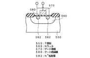
図18は一般的なアキュームレーションモードMOSバラクタからなる可変容量素子を示す断面図である。例えば、P型基板550の表面の素子分離膜により仕切られた素子形成領域にNウエル560が形成されており、この素子形成領域の表面上にゲート酸化膜580を介してポリシリコンゲート電極570が形成されている。そして、このゲート電極570の両側のNウエルの表面に1対のN+拡散層582が形成されている。これにより、ゲート絶縁膜580を間に挟むゲート電極570とNウエル560との間でMOSキャパシタが構成され、ゲート電極570とN+拡散層582とを接点とする可変容量素子が構成される。なお、通常のPチャネルMOSトランジスタの場合には、Nウエル560の表面に形成される1対の拡散層がP+導電型である。
【0003】
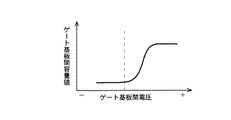
図19は横軸にゲート基板間電圧をとり、縦軸にゲート基板間容量値をとって、図18に示すアキュームレーションモードMOSバラクタの高周波C−V特性を示すグラフ図である。このアキュームレーションモードMOSバラクタの高周波C−V特性は、ゲート基板間電圧として負電圧が印加された場合は、Nウエル560の表面の空乏層が基板550側に広がるため、ゲート基板間容量値がゲート酸化膜580と空乏層との直列回路の容量値となり、ゲート基板間容量値が減少していく。更に、ゲート基板間に印加する負電位の絶対値を大きくしていくと、空乏層幅が広がる距離は飽和するため、ゲート基板間容量値も最小値に飽和する。逆に、ゲート基板間電圧が負電位側から正電位側に上げていくと、空乏層が狭まり、ゲート基板間容量値が増加して行く。このゲート基板間に印加する正電位の絶対値を上げていくと、Nウエル560の表面に蓄積層が形成されて、ゲート基板間容量値は、ゲート酸化膜580により決まる容量値に飽和する。
【0004】
このように、可変容量素子は、ゲート電極570とN+拡散層582との間に印加する電圧によりゲート基板間容量値が変化し、電圧制御発信器等の共振周波数を所定値に設定するために、容量値を外部電圧で変化させることができる容量素子として使用される。
【0005】
而して、この電圧制御可変容量素子の形状・大きさをどのようなものにすべきかを設計する際に、全ての素子を作り込んで特性を評価することには限界があり、このため、従来、可変容量素子の等価回路を作成して、この等価回路を使用して、数値計算により可変容量素子の形状寸法と特性を評価している。
【0006】
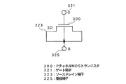
図20はこの可変容量素子の従来の等価回路を示し、図21はこの等価回路のCV特性を示す。この従来の等価回路は、PチャネルMOSトランジスタ300のソースドレイン(SD)端子323を同電位接続し、このソースドレイン端子323を基板端子325に接続した構造を有し、ゲート電極321と基板端子325との間のゲート基板間電圧を変化させることにより、ゲート基板間容量値が変化する。
【0007】
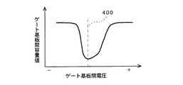
通常のPMOSトランジスタをそのまま使用している従来の等価回路は、ゲート電極に電圧を印加すると、基板表面の電位が変化し、それに伴って、蓄積状態、空乏状態及び反転状態に変化する。このため、ゲート基板間電圧が正電位であって、蓄積状態又は空乏層が伸びている状態の場合は、つまり、図21の破線400にて示す電位(閾値電圧)よりもゲート基板間電圧が高い場合は、ゲート基板間電位に依存した容量変化が得られる。
【0008】
【発明が解決しようとする課題】
しかしながら、ゲート基板間電圧を閾値電圧より下げていくと、ソースドレイン領域から少数キャリアのホールが供給されて、反転層が形成され始める。この反転層の形成のため、ゲート基板間電圧が下がるほど、ゲート基板間容量値が増加する。このように、従来のアキュームレーションモードバラクタの等価回路の場合には、ゲート基板間電圧が図21の破線400にて示す閾値電位よりも負電位側に入ると、ゲート基板間容量値の増加が生じてしまう。
【0009】
このように、従来の等価回路のCV特性は、図21に示すように、可変容量を制御するバイアス電圧とバラクタ容量との関係が、図21の破線400で示すゲート基板間電圧を境に逆転するという問題がある。この逆転現象は、従来モデルをPLL(Phase−Locked Loop:位相同期ループ)回路のVCO(Voltage−Controlled Oscillator:電圧制御発振器)の可変容量として使用した場合に特に問題となる。例えば、位相の遅れを修正する(周波数を上げる)ために、バラクタのゲート基板間電圧(バイアス)を下げて、容量値を下げようとした場合に、破線400で示す電位までは、ゲート基板間電位を下げることにより正常にゲート基板間容量値が減少して周波数が上昇する。
【0010】
しかしながら、更に位相に遅れが生じた場合に、バラクタのバイアスを更に下げようとすると、破線400で示す電位よりも負電位側に入るため、ゲート基板間電圧の低下と共に、ゲート基板間容量値が増加してしまう。このため、逆に位相が遅れてしまうという問題点がある。そうすると、PLL回路では、更に、バラクタのバイアスを下げるように動作し、ゲート基板間容量値が更に増加する。このような動作が繰り返されて、位相制御ができなくなってしまう。
【0011】
このように、従来のモデルでは、電圧制御可変容量素子(バラクタ)を表現できるバイアス範囲が、破線400で示す電位よりも正電位側の狭い範囲でしか使用できないという問題点がある。
【0012】
本発明はかかる問題点に鑑みてなされたものであって、電圧制御可変容量素子のCV特性を含む回路動作特性を高精度でシミュレーションすることができ、電圧制御可変容量素子を使用した回路の設計を極めて容易にすることができる電圧制御可変容量素子の等価回路を提供することを目的とする。
【0013】
【課題を解決するための手段】
本発明に係る電圧制御可変容量素子の等価回路は、ソース及びドレインが相互に接続されたMOSトランジスタと、前記MOSトランジスタのソースドレイン端子と基板端子との間に接続された第1の電圧源と、前記MOSトランジスタのゲート電極と前記基板との間に接続された固定容量とを有し、前記MOSトランジスタのゲート電極が接続されたゲート端子と、前記基板端子との間の容量特性により電圧制御可変容量素子の素子特性をシミュレーションするものであることを特徴とする。
【0014】
この電圧制御可変容量素子の等価回路において、更に、前記ゲート端子と、前記ゲート電極との間に接続された第2の電圧源を有することができる。
【0015】
前記MOSトランジスタは、例えば、PチャネルMOSトランジスタである。また、シミュレーションする前記電圧制御可変容量素子の素子特性は、例えば、ゲート基板間電圧Vとゲート基板間容量Cとの間のCV特性である。
【0016】
このCV特性は、前記固定容量の容量値を調節して、前記CV特性を全体的にゲート基板間容量値を高める方向に調整することができる。また、前記第1の電圧源の電圧値を調節して、反転層が発生するゲート基板間電圧を、負電圧方向にシフトさせるように調整することができる。更に、前記第2の電圧源の電圧値を調節して、前記CV特性を全体的にゲート基板間電圧値を正電位側に高める方向に調整することができる。更にまた、前記等価回路の回路特性を、Bsim3シミュレータを使用してシミュレーションすることができる。
【0017】
【発明の実施の形態】
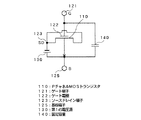
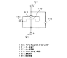
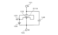
以下、本発明の実施形態について、添付の図面を参照して具体的に説明する。図1は本発明の第1実施形態に係る電圧制御可変容量素子の等価回路を示す回路図である。この等価回路は、可変容量を表現するPチャネルMOSトランジスタ110のゲート電極122にゲート端子121が接続され、基板電位の基板端子125とゲート端子121との間に、固定容量140がPチャネルMOSトランジスタ110と並列になるように接続されている。また、PチャネルMOSトランジスタ110のソースドレインはソースドレイン端子123に共通接続されて同一電位となっており、このソースドレイン端子123と基板端子125との間に、基板端子125側が正電位となる第1の電圧源130が接続されている。
【0018】
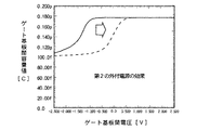
図2はこのように構成された等価回路におけるCV特性を示す。図2の横軸は、ゲート端子121と基板端子125との間に印加されたゲート基板間電圧であり、縦軸はそのときのゲート基板間容量である。本発明においては、ソースドレイン端子123と基板端子125との間に、バイアスを印加する第1の電圧源130をPチャネルMOSトランジスタ110に並列になるように接続しているので、反転層の形成電圧が負電圧方向(図2の白抜き矢印にて示す)にシフトされる。即ち、従来、図21に示すように、破線400にて示す電位より低いゲート基板間電圧では反転層が形成されてゲート基板間容量値が上昇してしまったが、本発明においては、この反転層が形成される電位を図2の破線610で示す電位まで、負電位側にシフトすることができる。このため、図2の破線610と破線660とで挟まれた電圧範囲600では、図19に示す実際の電圧制御可変容量素子のCV特性と等価なCV特性となる。また、固定容量140はトランジスタの寄生容量を表現するものであり、図19の負電位側のゲート基板間容量値が最小となるフラットな部分の容量(フリンジング容量)を表現するものである。
【0019】
本発明においては、このような等価回路をモデルとして、回路シミュレータにより、所望の特性が得られる電圧制御可変容量素子の形状寸法を求める。このような回路シミュレータ用のモデルとしては、Bsim3というカリフォルニア大学バークレイ校のデバイスグループが開発し発展させたものが周知である。このBsimモデルは、基本的には、物理的モデルであるが、回路シミュレータ用モデルとしての性格を考慮して、計算時間の短縮、収束性の改善の見地から、随所に大胆な近似を取り入れ、近似による精度の劣化を救うため、多くのフィッティングパラメータを導入している。
【0020】
この場合に、第1の電圧源130をソースドレイン端子123と基板端子125との間に付加したことよって生じるPチャネルMOSトランジスタ110の閾値電圧の変移は、Bsim3の閾値電圧を表現するパラメータによってフィッティングを行う。また、通常のMOSトランジスタモデルのソース容量及びドレイン容量を表現するBsim3のパラメータを殆どゼロに変えることで、可変容量以外の容量の影響を最小にする。フリンジング容量等の表現は、PチャネルMOSトランジスタ110に並列接続された固定容量140によってフィッティングを行う。
【0021】
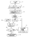
図3はこのBsim3によるMOSバラクタの等価回路の作成工程を示すフローチャート図である。モデル作成を開始し(ステップS1)、Bsim3に内蔵されているPチャネルMOSトランジスタのひな形を使用して、図1に示す等価回路の各部品を組み立てる(ステップS2)。そして、Bsim3モデルパラメータのうち、可変容量を表現するパラメータ以外の容量を殆ど0(ゼロ)にする(ステップS3)。その後、等価回路の初期値を設定する(ステップS4)。そして、回路シミュレーションを行い(ステップS5)、図1に示す等価回路のCV特性を求める。一方、図18に示す電圧制御可変容量素子の実デバイスのCV特性の測定データを求め(ステップS6)、この実測データと回路シミュレーション結果とを読み込み(ステップS7)、両者を比較して回路シミュレーション結果におけるフィッティング精度を求める(ステップS8)。このフィッティング精度が悪い(No)場合には、固定容量140及び第1の電圧源130の各値と、Bsim3のパラメータとを調整し(ステップS9)、再度、回路シミュレーションを行う(ステップS5)。このような実測データと回路シミュレーション結果との比較を繰り返し、フィッティング精度が十分である(Yes)と判断された場合には、そのときのパラメータによりMOSバラクタ(可変容量素子)の等価回路が完成する。このようにして求められた電圧制御可変容量素子の等価回路を使用して、所望の特性を有する電圧制御可変容量素子を設計する。
【0022】
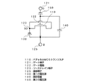
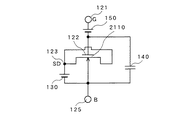
図4は本発明の第2実施形態に係る電圧制御可変容量素子の等価回路を示す回路図である。本実施形態が、図1に示す第1実施形態と相違する点は、ゲート端子121と、PチャネルMOSトランジスタ110のゲート電極122との間に、第2の電圧源150をゲート電極122側が正電位になるように接続したことにある。
【0023】
この第2実施形態の等価回路では、第1の電圧源130をソースドレイン端子123と基板端子125との間に付加したことによって生じる閾値電圧の変移を、Bsim3の閾値電圧を表現するパラメータを調整することに加え、第2の電圧源150をゲート端子121とゲート電極122との間に直列に接続し、この第2の電圧源150のパラメータを調整することとの組み合わせにより、より柔軟にフィッティングすることが可能となる。即ち、この第2実施形態においては、ゲートに対して直列に挿入した第2の電圧源150によって、PチャネルMOSトランジスタ110の閾値電圧を操作することが可能となり、Bsim3の閾値を制御するパラメータと組み合わせることにより、柔軟な設定が可能となる。その結果、反転層が発生しない可変容量素子(バラクタ)の実デバイスのC−V特性により一層近似したCV特性の等価回路が得られる。
【0024】
次に、この等価回路に使用した回路部品を使用してシミュレートした場合のフィッティング効果について説明する。図1又は図4に示す実施形態の等価回路の各回路部品がCV特性シミュレーションに及ぼす効果については、以下のとおりである。先ず、外付けの固定容量140は、CV特性全体の容量値を増減させる。また、第1の電圧源130は反転層発生電圧をシフトさせる。更に、第2の電圧源150はCV特性の立ち上がり位置をシフトさせる。
【0025】
一方、Bsim3のモデルパラメータがCV特性シミュレーションに与える効果については、以下のとおりである。先ず、DLCが可変容量素子の振幅を増減させる。また、VTH0はCV特性の立ち上がり位置をシフトさせると共に、その調整によりCV特性のコーナーの角度を操作することができる。更に、K1はCV特性の立ち上がりの傾斜角と振幅を増減させる。
【0026】
但し、部品及びモデルパラメータは、互いに依存関係を有する。このため、以上の説明は、各値を変えたときに、シミュレーション結果が見かけ上で最も大きく特性が変化する箇所を述べたものであり、各部品と特性関係が1対1には対応しない。
【0027】
このような各パラメータの特性を利用して、フィッティングを行う。フィッティングとは、可変容量素子の実デバイスの高周波測定により得られたCV特性に、回路シミュレーションの実行結果が要求精度を満たす程度に一致するように、等価回路の各部品の値を調節して追い込むことである。以下、具体的なフィッティング方法について説明する。
【0028】
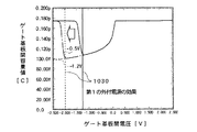
先ず、基本的なPチャネルMOSトランジスタのCV特性は図5に示すとおりである。図5は、図20に示す従来の等価回路、即ち基本的なPチャネルMOSトランジスタ(L=0.16μm、W=100μm)の等価回路のCV特性シミュレーション結果(実線)と、電圧制御可変容量素子の実デバイスのCV特性測定データ(一点鎖線、◆)とを比較して示す。前述のように、PチャネルMOSトランジスタのCV特性は、反転層の影響によって負電位(約−0.3V)側の反転層発生電圧(線分1030で示す)で、ゲート基板間容量値の増加が生じている。また、容量立ち上がり電位(線分1010で示す)が大きく正電位側にあり、しかも全体の容量が小さい。
【0029】
次いで、Bsim3モデルパラメータのうち、容量を表現するパラメータを殆どゼロ(0)にする。Bsim3モデルパラメータの可変容量を表現するパラメータ以外のパラメータとしては、CGSO(ゲートソース間寄生容量)、CGDO(ゲートドレイン間寄生容量)、CJ(フリンジ電界容量)、CJSW(ゼロバイアス・バルク接合側面容量)等がある。これらのパラメータをシミュレーションで影響が出ない範囲で小さくする。これは、MOS可変容量素子が、PチャネルMOSトランジスタと構造が相違するため、Bsim3パラメータの値(特に、容量を表現するパラメータ)によって、意図しない作用が発生することを防止するためである。なお、この構造の相違は、前述の如く、基板表面のNウエルに作り込まれた可変容量素子のソースドレイン拡散層がN+型であり、Nウエルとソースドレイン拡散層とは同電位であるのに対し、PチャネルMOSトランジスタの場合は、Nウエルの表面に形成されたソースドレインがP+拡散層であることである。
【0030】
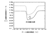
次に、図6に示すように、従来の等価回路(図20:Pチャネルトランジスタ300のみ)に対し、外付けの固定容量140を付加した場合のシミュレーション結果について説明する。なお、図6において、図1と同一構成物には同一符号を付してある。この図6に示す等価回路の回路シミュレーションにより求めたCV特性を図7に示す。図7において、実線が外付け容量140がない場合のシミュレーション結果であり、破線が0.07pFの容量をもつ外付け容量140を付加した場合のシミュレーション結果である。但し、Bsim3モデルには、Bsim3のモデルパラメータの可変容量を表現するパラメータ以外のパラメータを殆どゼロにしている。
【0031】
この図7に示すように、外付け容量140を付加すると、ゲート基板間容量値が全体的に(全てのゲート基板間電圧で)増加する。
【0032】
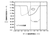
次に、Bsim3のモデルパラメータの調整によるシミュレーション結果について説明する。Bsim3のVTH0は、閾値電圧を調整するパラメータである。図8に示すように、VTH0の値を負の値にすると、容量が立ち上がる位置(線分1020で示す)のゲート基板間電圧が負電圧方向にシフトする。図中、破線は、VTH0を約−1.5に調整した場合のものである。
【0033】
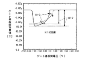
K1はモデルの閾値に対する係数である。図9に示すように、K1の値を増加させると、図中破線にて示すように、CV特性の傾き800がなだらかになり(落ち込みが緩やかになり)、容量値の最大値からの落ち込みを示す振幅810が減少する。図中、破線はK1を約1.1に調整したものである。
【0034】
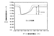
DLCはCV特性からのゲート長オフセット・フィッティング・パラメータである。図10に示すように、DLCの値を減少させると、図中破線にて示すように、CV特性の波形における最大容量値の増加を示す振幅910が増加する。図中、破線はDLCを約2.0×10⁻⁸に調節している。
【0035】
次に、第1の電圧源130の付加によるシミュレーションへの効果について説明する。図1に示すように、図6の等価回路に対し、外付けの第1の電圧源130を付加すると、その回路シミュレーションにより求まるCV特性は図11に示すようになる。図11において、実線は第1の電圧源がない場合(図7の破線と同一)、一点鎖線及び破線は第1の電圧源130を付加した場合の回路シミュレーションによるCV特性である。この一点鎖線は、第1の電圧源130として、−0.5Vを印加した場合、破線は−1.2Vを印加した場合のシミュレーション結果である。この図11に示すように、第1の電圧源130を付加することにより、反転層発生電圧(線分1030で示す)をバラクタの制御電圧の範囲外(この場合は、−1.5V以下)まで負電圧方向にシフトさせることができる。
【0036】
そして、▲1▼容量を表現するパラメータを殆どゼロにする、▲2▼外付け容量140の付加、▲3▼Bsim3モデルパラメータの調整の各工程を繰り返して、パラメータを調整することにより、測定データとシミュレーション結果との相違が、要求精度(例えば、±10%以内)を満たすまで、パラメータを追い込んでいく。
【0037】
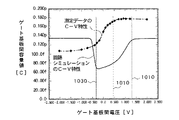
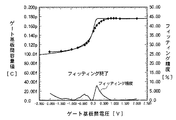
図12は横軸にゲート基板間電圧をとり、縦軸にゲート基板間容量値をとって、フィッティング終了時のCV特性を示す。図中、◆は実デバイスの測定データのCV特性であり、実線はパラメータを回路シミュレーションにより求めた等価回路(図1に示す)のCV特性である。そして、図中、フィッティング精度も合わせて示す。この図12に示すように、実測データと、シミュレーション結果とは、高精度で一致しており、本発明の第1実施形態の等価回路は、フィッティング精度が高い(誤差が小さい)ことがわかる。
【0038】
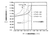
図13はCV特性に対するVTH0の影響を示すグラフ図である。Bsim3のモデルパラメータのVTH0を負の値にしてその絶対値を大きくしていくと、ゲート基板間容量値の立ち上がり位置1020が負電位側にシフトすると共に、CV特性の波形のコーナー部1010の角度が緩やかになるように変化する。図12に示すように、図1に示す等価回路のシミュレーション結果はCV特性の波形のコーナー部が実測データよりも曲率が小さく急であり、この部分でフィッティング精度が若干悪い。これに対し、図13に示すように、VTH0を負の値にすることにより、このコーナー部1010の曲率を大きくしてなだらかにすることができる。しかし、前述の如く、VTH0を負の値にすることにより、容量の立ち上がり位置1020が負電位側にシフトしてしまう。
【0039】
そこで、図4に示す第2実施形態の等価回路のように、第2の電圧源150を設ける。図14は、第2の電圧源150として、約+1.6Vを印加した場合のCV特性のシミュレーション結果(破線)を、第2の電圧源150を設けない場合(実線)と比較して示す。この図14に示すように、第2の電圧源150を設けることにより、立ち上がり位置を正電位側にシフトさせる効果があり、VTH0により負電位側にシフトした容量の立ち上がり位置1020の電圧を打ち消す作用がある。このため、第2の電圧源150を設けることにより、CV特性のパターン形状をそのまま維持しつつ、CV特性のパターン全体をゲート基板間電圧の正電位側にシフトすることができる。
【0040】
なお、Bsim3のモデルパラメータのVTH0以外のパラメータK1及びDLCも、CV特性の振幅及び容量変化を操作するが、VTH0と同様に容量の立ち上がり位置1020も変化させてしまう。この場合も、第2の電圧源150を設けることにより、これらのパラメータを操作したときの容量の立ち上がり位置1020の変化を打ち消すことができ、フィッティング作業を柔軟に行うことができ、フィッティング作業が容易になる。
【0041】
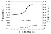
図15は図4に示す第2実施形態の等価回路において、上述の如くしてフィッティングした場合のフィッティング精度を示すグラフ図である。この図15に示すように、可変容量素子の実デバイスのCV特性(◆)と、等価回路のシミュレーション結果によるCV特性とは極めてよく一致し、フィッティング精度が極めて高い(誤差が極めて小さい)。
【0042】
上述の如く、本発明の等価回路は、ソースドレイン端子123と基板端子125との間に、第1の電圧源130を、PチャネルMOSトランジスタ110に並列になるように接続したことにより、図2に示すように、反転層が発生するバイアス電圧を電圧制御可変容量素子(バラクタ)の制御電圧の範囲600から外側610まで負電圧方向にシフトさせることができ、また、Bsim3における通常のMOSトランジスタモデルのソース容量及びドレイン容量の影響を防止するため、Bsim3のソース容量及びドレイン容量を表現するパラメータを殆どゼロにし、更にフリンジング容量等の表現は、固定容量140をゲート基板間に並列接続してフィッティングできるようにしており、更に、第1の電圧源130を設けることによって、PチャネルMOSトランジスタの閾値電圧が変化するのを、Bsim3の閾値電圧を制御するパラメータによって調整することができる。
【0043】
また、ゲートに対して直列に第2の電圧源150を挿入することにより、PチャネルMOSトランジスタの閾値電圧を操作することが可能となり、Bsim3の閾値を制御するパラメータと組み合わせることにより、柔軟なフィッティングが可能となる。
【0044】
なお、本発明における等価回路において、MOSトランジスタ110の導電型はPチャネルに限らず、Nチャネルでもよく、シミュレーションすべき可変容量素子に応じて適宜のMOSトランジスタを採用することができる。図16は、図1に示す実施形態において、PチャネルMOSトランジスタ110の代わりに、NチャネルMOSトランジスタ2110を使用した場合の実施形態を示す回路図である。この等価回路においては、第1の電圧源130の極性が反転されている。本実施形態においても、図1に示す実施形態と同様の作用効果を有する。
【0045】
図17は、図4に示す実施形態において、PチャネルMOSトランジスタ110の代わりに、NチャネルMOSトランジスタ2110を使用した場合の実施形態を示す回路図である。この等価回路においては、第1の電圧源130及び第2の電圧源150の極性が反転されている。本実施形態においても、図4に示す実施形態と同様の作用効果を有する。
【0046】
【発明の効果】
以上詳述したように、従来の等価回路では、図21に示すCV特性のように、ゲート基板間電圧が閾値よりも負電位側に入ると反転層が形成されてゲート基板間容量値の増大が発生してしまうのに対し、本発明の等価回路によれば、図2に示すように、CV特性は反転層が発生するバイアス電圧を、電圧制御可変容量素子の制御電圧の範囲よりも外側(より低電位側)の電圧まで、負電位側にシフトさせることができ、その結果、実際の電圧制御可変容量素子のCV特性と等価なCV特性を得ることができる。よって、この本発明の等価回路を使用して、実デバイスである電圧制御可変容量素子のCV特性を含む回路動作特性を極めて高精度でシミュレーションすることができ、本発明は、電圧制御可変容量素子を使用した回路の設計の迅速化及び低コスト化に多大の貢献をなす。
【図面の簡単な説明】
【図1】本発明の第1実施形態に係る電圧制御可変容量素子の等価回路を示す回路図である。
【図2】本実施形態の等価回路のCV特性を示すグラフ図である。
【図3】本実施形態の動作を示すフローチャート図である。
【図4】本発明の第2実施形態に係る電圧制御可変容量素子の等価回路を示す回路図である。
【図5】図20及び図21に示す従来の等価回路のシミュレーション結果のCV特性と、実デバイスのCV特性の測定データとを比較して示すグラフ図である。
【図6】外付けの固定容量140を付加した等価回路を示す回路図である。
【図7】CV特性に及ぼす外付けの固定容量140の影響を示すグラフ図である。
【図8】CV特性に及ぼすBsim3パラメータVTH0の影響を示すグラフ図である。
【図9】CV特性に及ぼすBsim3パラメータK1の影響を示すグラフ図である。
【図10】CV特性に及ぼすBsim3パラメータDLCの影響を示すグラフ図である。
【図11】CV特性に及ぼす第1の電圧源130の影響を示すグラフ図である。
【図12】第1実施形態の等価回路のフィッティング精度を示すグラフ図である。
【図13】CV特性に及ぼすBsim3パラメータVTH0の影響を示すグラフ図である。
【図14】CV特性に及ぼす第2の電圧源150の影響を示すグラフ図である。
【図15】第2実施形態の等価回路のフィッティング精度を示すグラフ図である。
【図16】本発明の第3実施形態に係る電圧制御可変容量素子の等価回路を示す回路図である。
【図17】本発明の第4実施形態に係る電圧制御可変容量素子の等価回路を示す回路図である。
【図18】電圧制御可変容量素子の構造を示す断面図である。
【図19】この電圧制御可変容量素子のCV特性を示すグラフ図である。
【図20】従来の等価回路を示す回路図である。
【図21】この従来の等価回路のCV特性を示すグラフ図である。
【符号の説明】
110:PチャネルMOSトランジスタ
121:ゲート端子
122:ゲート電極
123:ソースドレイン端子
125:基板端子
130:第1の電圧源
140:固定容量
150:第2の電圧源
300:PチャネルMOSトランジスタ
321:ゲート端子
323:ソースドレイン端子
325:基板端子
550:P基板
560:Nウエル
570:ゲート電極
580:ゲート絶縁膜
582:N+拡散層
2110:NチャネルMOSトランジスタ[0001]
TECHNICAL FIELD OF THE INVENTION
The present invention relates to an equivalent circuit for simulating a voltage variable capacitance element that changes a capacitance value with an external voltage in order to set a resonance frequency of a voltage controlled oscillator or the like to a predetermined value.
[0002]
[Prior art]
FIG. 18 is a cross-sectional view showing a variable capacitance element composed of a general accumulation mode MOS varactor. For example, an N well 560 is formed in an element formation region on the surface of a P-type substrate 550 separated by an element isolation film, and a polysilicon gate electrode 570 is formed on the surface of the element formation region via a gate oxide film 580. Is formed. Then, a pair of N-wells + A diffusion layer 582 is formed. Thereby, a MOS capacitor is formed between gate electrode 570 and N well 560 with gate insulating film 580 interposed therebetween, and gate electrode 570 and N + A variable capacitance element having the diffusion layer 582 as a contact point is configured. In the case of a normal P-channel MOS transistor, a pair of diffusion layers formed on the surface of N well + Conductive type.
[0003]
FIG. 19 is a graph showing the high-frequency CV characteristics of the accumulation mode MOS varactor shown in FIG. 18, with the horizontal axis representing the voltage between the gate substrates and the vertical axis representing the capacitance between the gate substrates. The high frequency CV characteristic of the accumulation mode MOS varactor is such that when a negative voltage is applied as a gate-substrate voltage, the depletion layer on the surface of the N-well 560 spreads to the substrate 550 side, so that the gate-substrate capacitance value is reduced. The capacitance value becomes the capacitance value of the series circuit of the gate oxide film 580 and the depletion layer, and the capacitance value between the gate substrates decreases. Further, as the absolute value of the negative potential applied between the gate substrates is increased, the distance at which the width of the depletion layer spreads is saturated, so that the capacitance value between the gate substrates is also saturated to the minimum value. Conversely, as the gate-substrate voltage increases from the negative potential side to the positive potential side, the depletion layer becomes narrower and the gate-substrate capacitance value increases. As the absolute value of the positive potential applied between the gate substrates is increased, an accumulation layer is formed on the surface of N well 560, and the capacitance between the gate substrates saturates to the capacitance determined by gate oxide film 580.
[0004]
As described above, the variable capacitance element includes the gate electrode 570 and the N + A capacitance element that changes the capacitance value with an external voltage in order to change the capacitance value between the gate substrates according to the voltage applied to the diffusion layer 582 and to set the resonance frequency of a voltage controlled oscillator or the like to a predetermined value Used as
[0005]
Therefore, when designing the shape and size of the voltage-controlled variable capacitance element, there is a limit in evaluating all the elements and evaluating the characteristics. 2. Description of the Related Art Conventionally, an equivalent circuit of a variable capacitance element is created, and the shape and size and characteristics of the variable capacitance element are evaluated by numerical calculation using the equivalent circuit.
[0006]
FIG. 20 shows a conventional equivalent circuit of this variable capacitance element, and FIG. 21 shows CV characteristics of this equivalent circuit. This conventional equivalent circuit has a structure in which a source / drain (SD) terminal 323 of a P-channel MOS transistor 300 is connected to the same potential, and the source / drain terminal 323 is connected to a substrate terminal 325. The gate electrode 321 and the substrate terminal 325 By changing the gate-substrate voltage between the above, the capacitance value between the gate substrates changes.
[0007]
In a conventional equivalent circuit using a normal PMOS transistor as it is, when a voltage is applied to the gate electrode, the potential on the substrate surface changes, and accordingly, the state changes to an accumulation state, a depletion state, and an inversion state. Therefore, when the gate-to-substrate voltage is a positive potential and the storage state or the depletion layer is extended, that is, the gate-to-substrate voltage is higher than the potential (threshold voltage) shown by the broken line 400 in FIG. When it is high, a capacitance change depending on the gate-substrate potential is obtained.
[0008]
[Problems to be solved by the invention]
However, when the gate-substrate voltage is lowered below the threshold voltage, minority carrier holes are supplied from the source / drain region, and the inversion layer starts to be formed. Due to the formation of the inversion layer, the capacitance value between the gate substrates increases as the voltage between the gate substrates decreases. As described above, in the case of the equivalent circuit of the conventional accumulation mode varactor, when the gate-substrate voltage falls on the negative potential side with respect to the threshold potential shown by the broken line 400 in FIG. Will happen.
[0009]
Thus, as shown in FIG. 21, the CV characteristic of the conventional equivalent circuit is such that the relationship between the bias voltage for controlling the variable capacitance and the varactor capacitance reverses at the gate-substrate voltage indicated by the broken line 400 in FIG. There is a problem of doing. This reversal phenomenon becomes a problem particularly when the conventional model is used as a variable capacitor of a VCO (Voltage-Controlled Oscillator) of a PLL (Phase-Locked Loop) circuit. For example, in order to correct the phase delay (increase the frequency), the voltage (bias) between the gate and the substrate of the varactor is reduced to reduce the capacitance value. By lowering the potential, the capacitance value between the gate substrates normally decreases, and the frequency increases.
[0010]
However, if the phase of the varactor is further reduced when the phase is further delayed, the varactor enters a negative potential side with respect to the potential shown by the broken line 400. Will increase. Therefore, there is a problem that the phase is delayed. Then, the PLL circuit operates to further lower the bias of the varactor, and the capacitance value between the gate substrates further increases. Such an operation is repeated, and phase control cannot be performed.
[0011]
As described above, the conventional model has a problem that the bias range in which the voltage-controlled variable capacitance element (varactor) can be expressed can be used only in a narrower range on the positive potential side than the potential indicated by the broken line 400.
[0012]
The present invention has been made in view of such a problem, and can simulate circuit operation characteristics including CV characteristics of a voltage-controlled variable capacitance element with high accuracy, and design a circuit using the voltage-controlled variable capacitance element. It is an object of the present invention to provide an equivalent circuit of a voltage-controlled variable capacitance element which can extremely easily perform the above.
[0013]
[Means for Solving the Problems]
An equivalent circuit of the voltage controlled variable capacitance element according to the present invention includes a MOS transistor having a source and a drain connected to each other, and a first voltage source connected between a source / drain terminal of the MOS transistor and a substrate terminal. A fixed capacitance connected between the gate electrode of the MOS transistor and the substrate, and controlling the voltage by a capacitance characteristic between the gate terminal connected to the gate electrode of the MOS transistor and the substrate terminal. It is characterized in that it simulates the element characteristics of a variable capacitance element.
[0014]
The equivalent circuit of the voltage-controlled variable capacitance element may further include a second voltage source connected between the gate terminal and the gate electrode.
[0015]
The MOS transistor is, for example, a P-channel MOS transistor. The element characteristics of the voltage-controlled variable capacitance element to be simulated are, for example, CV characteristics between a gate substrate voltage V and a gate substrate capacitance C.
[0016]
The CV characteristic can be adjusted by adjusting the capacitance value of the fixed capacitor so as to increase the capacitance value between the gate substrates as a whole. Further, by adjusting the voltage value of the first voltage source, the voltage between the gate substrates generated by the inversion layer can be adjusted to be shifted in the negative voltage direction. Further, by adjusting the voltage value of the second voltage source, it is possible to adjust the CV characteristic in the direction of increasing the gate-substrate voltage value to the positive potential side as a whole. Furthermore, the circuit characteristics of the equivalent circuit can be simulated using a Bsim3 simulator.
[0017]
BEST MODE FOR CARRYING OUT THE INVENTION
Hereinafter, embodiments of the present invention will be specifically described with reference to the accompanying drawings. FIG. 1 is a circuit diagram showing an equivalent circuit of the voltage controlled variable capacitance element according to the first embodiment of the present invention. In this equivalent circuit, a gate terminal 121 is connected to a gate electrode 122 of a P-channel MOS transistor 110 expressing a variable capacitance, and a fixed capacitance 140 is connected between a substrate terminal 125 and a gate terminal 121 at a substrate potential. 110 is connected in parallel. The source and drain of the P-channel MOS transistor 110 are commonly connected to the source / drain terminal 123 and have the same potential. Between the source / drain terminal 123 and the substrate terminal 125, the substrate terminal 125 side has a positive potential. One voltage source 130 is connected.
[0018]
FIG. 2 shows CV characteristics in the equivalent circuit thus configured. The horizontal axis in FIG. 2 is the voltage between the gate substrates applied between the gate terminal 121 and the substrate terminal 125, and the vertical axis is the capacitance between the gate substrates at that time. In the present invention, since the first voltage source 130 for applying a bias is connected between the source drain terminal 123 and the substrate terminal 125 so as to be in parallel with the P-channel MOS transistor 110, the inversion layer is formed. The voltage is shifted in the negative voltage direction (indicated by the white arrow in FIG. 2). That is, conventionally, as shown in FIG. 21, an inversion layer is formed at a gate-to-substrate voltage lower than the potential indicated by the broken line 400 to increase the gate-to-substrate capacitance value. The potential at which the layer is formed can be shifted to the negative potential side up to the potential indicated by the broken line 610 in FIG. Therefore, in the voltage range 600 sandwiched between the broken line 610 and the broken line 660 in FIG. 2, the CV characteristic is equivalent to the actual CV characteristic of the voltage-controlled variable capacitance element shown in FIG. The fixed capacitance 140 expresses the parasitic capacitance of the transistor, and expresses the capacitance (fringing capacitance) of the flat portion where the capacitance value between the gate substrates on the negative potential side in FIG. 19 is minimized.
[0019]
In the present invention, using such an equivalent circuit as a model, the shape and dimensions of a voltage-controlled variable capacitance element that can obtain desired characteristics are obtained by a circuit simulator. A well-known model for such a circuit simulator is Bsim3, which has been developed and developed by a device group at the University of California, Berkeley. Although this Bsim model is basically a physical model, it takes bold approximations everywhere from the viewpoint of shortening calculation time and improving convergence in consideration of the characteristics as a model for a circuit simulator. Many fitting parameters are introduced to save the degradation of accuracy due to approximation.
[0020]
In this case, the shift of the threshold voltage of the P-channel MOS transistor 110 caused by adding the first voltage source 130 between the source / drain terminal 123 and the substrate terminal 125 is determined by fitting a parameter expressing the threshold voltage of Bsim3. I do. Also, by changing the parameter of Bsim3 expressing the source capacitance and the drain capacitance of the normal MOS transistor model to almost zero, the influence of the capacitance other than the variable capacitance is minimized. The expression of the fringing capacitance and the like is performed by fitting with a fixed capacitance 140 connected in parallel to the P-channel MOS transistor 110.
[0021]
FIG. 3 is a flowchart showing a process of creating an equivalent circuit of a MOS varactor by using Bsim3. Model creation is started (step S1), and each component of the equivalent circuit shown in FIG. 1 is assembled using a model of a P-channel MOS transistor built in Bsim3 (step S2). Then, among the Bsim3 model parameters, the capacity other than the parameter expressing the variable capacity is set to almost 0 (step S3). After that, the initial value of the equivalent circuit is set (step S4). Then, a circuit simulation is performed (step S5), and CV characteristics of the equivalent circuit shown in FIG. 1 are obtained. On the other hand, measured data of the CV characteristic of the actual device of the voltage-controlled variable capacitance element shown in FIG. 18 is obtained (step S6), and the actually measured data and the circuit simulation result are read (step S7). Is determined (step S8). If the fitting accuracy is poor (No), the values of the fixed capacitor 140 and the first voltage source 130 and the parameter of Bsim3 are adjusted (Step S9), and the circuit simulation is performed again (Step S5). The comparison between the actual measurement data and the circuit simulation result is repeated, and when it is determined that the fitting accuracy is sufficient (Yes), an equivalent circuit of the MOS varactor (variable capacitance element) is completed with the parameters at that time. . Using the equivalent circuit of the voltage-controlled variable capacitance element thus obtained, a voltage-controlled variable capacitance element having desired characteristics is designed.
[0022]
FIG. 4 is a circuit diagram showing an equivalent circuit of the voltage-controlled variable capacitance element according to the second embodiment of the present invention. This embodiment is different from the first embodiment shown in FIG. 1 in that the second voltage source 150 is connected between the gate terminal 121 and the gate electrode 122 of the P-channel MOS transistor 110 on the gate electrode 122 side. That they are connected to a potential.
[0023]
In the equivalent circuit of the second embodiment, the shift of the threshold voltage caused by adding the first voltage source 130 between the source / drain terminal 123 and the substrate terminal 125 is adjusted by adjusting the parameter expressing the threshold voltage of Bsim3. In addition to the above, the second voltage source 150 is connected in series between the gate terminal 121 and the gate electrode 122 to adjust the parameters of the second voltage source 150, so that the fitting can be performed more flexibly. It is possible to do. That is, in the second embodiment, the threshold voltage of the P-channel MOS transistor 110 can be controlled by the second voltage source 150 inserted in series with the gate, and the parameter for controlling the threshold value of Bsim3 can be controlled. The combination enables flexible setting. As a result, an equivalent circuit having a CV characteristic more approximate to the CV characteristic of the actual device of the variable capacitance element (varactor) in which the inversion layer does not occur can be obtained.
[0024]
Next, a description will be given of a fitting effect when a simulation is performed using the circuit components used in the equivalent circuit. The effect of each circuit component of the equivalent circuit of the embodiment shown in FIG. 1 or 4 on the CV characteristic simulation is as follows. First, the external fixed capacitor 140 increases or decreases the capacitance value of the entire CV characteristic. The first voltage source 130 shifts the inversion layer generated voltage. Further, the second voltage source 150 shifts the rising position of the CV characteristic.
[0025]
On the other hand, the effect of the Bsim3 model parameter on the CV characteristic simulation is as follows. First, the DLC increases or decreases the amplitude of the variable capacitance element. In addition, VTH0 shifts the rising position of the CV characteristic, and the angle of the corner of the CV characteristic can be controlled by the adjustment. Further, K1 increases or decreases the inclination angle and amplitude of the rise of the CV characteristic.
[0026]
However, parts and model parameters have a dependency relationship with each other. For this reason, the above description describes the places where the simulation results apparently change the characteristics the most when the values are changed, and the characteristic relationship with each component does not correspond one-to-one.
[0027]
Fitting is performed using such characteristics of each parameter. The fitting is a process in which the values of the components of the equivalent circuit are adjusted to the CV characteristics obtained by high-frequency measurement of the actual device of the variable capacitance element so that the result of the circuit simulation matches the required accuracy. That is. Hereinafter, a specific fitting method will be described.
[0028]
First, the basic CV characteristics of the P-channel MOS transistor are as shown in FIG. FIG. 5 shows a simulation result (solid line) of the conventional equivalent circuit shown in FIG. 20, that is, an equivalent circuit of a basic P-channel MOS transistor (L = 0.16 μm, W = 100 μm), and a voltage-controlled variable capacitance element. And CV characteristic measurement data (dotted chain line, Δ) of the actual device. As described above, the CV characteristic of the P-channel MOS transistor is such that the capacitance between gate substrates increases due to the inversion layer generated voltage (indicated by line 1030) on the negative potential side (about -0.3 V) due to the influence of the inversion layer. Has occurred. In addition, the capacitance rising potential (indicated by line 1010) is large and on the positive potential side, and the overall capacitance is small.
[0029]
Next, among the Bsim3 model parameters, the parameter expressing the capacity is set to almost zero (0). The Bsim3 model parameters other than the parameter expressing the variable capacitance include CGSO (parasitic capacitance between gate and source), CGDO (parasitic capacitance between gate and drain), CJ (fringe electric field capacitance), and CJSW (zero bias bulk junction side surface capacitance). ). These parameters are reduced as long as they are not affected by the simulation. This is to prevent an unintended operation from occurring due to the value of the Bsim3 parameter (particularly, a parameter expressing capacitance) because the structure of the MOS variable capacitance element is different from that of the P-channel MOS transistor. The difference in structure is that the source / drain diffusion layer of the variable capacitance element formed in the N well on the substrate surface is N + In the case of a P-channel MOS transistor, the source / drain formed on the surface of the N-well has the same potential as the source / drain diffusion layer. + That is, it is a diffusion layer.
[0030]
Next, a description will be given of a simulation result when an external fixed capacitor 140 is added to a conventional equivalent circuit (FIG. 20: only the P-channel transistor 300) as shown in FIG. In FIG. 6, the same components as those in FIG. 1 are denoted by the same reference numerals. FIG. 7 shows CV characteristics obtained by circuit simulation of the equivalent circuit shown in FIG. In FIG. 7, the solid line is the simulation result when there is no external capacitance 140, and the broken line is the simulation result when the external capacitance 140 having a capacitance of 0.07 pF is added. However, in the Bsim3 model, parameters other than the parameter expressing the variable capacity of the Bsim3 model parameters are almost zero.
[0031]
As shown in FIG. 7, when an external capacitor 140 is added, the capacitance between gate substrates increases as a whole (at all gate-substrate voltages).
[0032]
Next, a simulation result by adjusting the model parameter of Bsim3 will be described. VTH0 of Bsim3 is a parameter for adjusting the threshold voltage. As shown in FIG. 8, when the value of VTH0 is a negative value, the gate-substrate voltage at the position where the capacitance rises (indicated by line segment 1020) shifts in the negative voltage direction. In the figure, the broken line shows the case where VTH0 is adjusted to about -1.5.
[0033]
K1 is a coefficient for the threshold value of the model. As shown in FIG. 9, when the value of K1 is increased, the slope 800 of the CV characteristic becomes gentle (decreases gradually) as indicated by a broken line in the figure, and the capacitance value decreases from the maximum value. The indicated amplitude 810 decreases. In the drawing, the broken line is obtained by adjusting K1 to about 1.1.
[0034]
DLC is a gate length offset fitting parameter from CV characteristics. As shown in FIG. 10, when the value of DLC is decreased, as shown by the broken line in the figure, the amplitude 910 indicating the increase in the maximum capacitance value in the waveform of the CV characteristic increases. In the figure, the dashed line indicates that DLC is about 2.0 × 10 -8 It is adjusted to.
[0035]
Next, the effect of the addition of the first voltage source 130 on the simulation will be described. As shown in FIG. 1, when an external first voltage source 130 is added to the equivalent circuit of FIG. 6, the CV characteristics obtained by the circuit simulation are as shown in FIG. In FIG. 11, the solid line is the CV characteristic by the circuit simulation when the first voltage source is not provided (the same as the broken line in FIG. 7), and the dashed line and the broken line are the case where the first voltage source 130 is added. The dashed-dotted line is the simulation result when -0.5 V is applied as the first voltage source 130, and the broken line is the simulation result when -1.2V is applied. As shown in FIG. 11, by adding the first voltage source 130, the inversion layer generated voltage (indicated by the line segment 1030) is out of the range of the varactor control voltage (in this case, -1.5 V or less). Up to the negative voltage.
[0036]
By repeating the steps of (1) making the parameter expressing the capacity almost zero, (2) adding the external capacity 140, and (3) adjusting the Bsim3 model parameters, the measurement data is obtained by adjusting the parameters. The parameters are adjusted until the difference between the simulation result and the simulation result satisfies the required accuracy (for example, within ± 10%).
[0037]
FIG. 12 shows the CV characteristic at the end of the fitting, with the horizontal axis representing the voltage between the gate substrates and the vertical axis representing the capacitance between the gate substrates. In the figure, ◆ indicates the CV characteristic of the measurement data of the actual device, and the solid line indicates the CV characteristic of the equivalent circuit (shown in FIG. 1) whose parameters were obtained by circuit simulation. In the figure, the fitting accuracy is also shown. As shown in FIG. 12, the measured data and the simulation result match with high accuracy, and it can be seen that the equivalent circuit of the first embodiment of the present invention has high fitting accuracy (small error).
[0038]
FIG. 13 is a graph showing the effect of VTH0 on CV characteristics. When VTH0 of the model parameter of Bsim3 is set to a negative value and its absolute value is increased, the rising position 1020 of the gate-substrate capacitance value shifts to the negative potential side and the angle of the corner 1010 of the CV characteristic waveform. Changes so as to be gentle. As shown in FIG. 12, the simulation result of the equivalent circuit shown in FIG. 1 shows that the corner of the waveform of the CV characteristic has a smaller curvature and is steeper than the measured data, and the fitting accuracy is slightly poor in this part. On the other hand, as shown in FIG. 13, by setting VTH0 to a negative value, the curvature of the corner portion 1010 can be increased to make it smooth. However, as described above, by setting VTH0 to a negative value, the rising position 1020 of the capacitance is shifted to the negative potential side.
[0039]
Therefore, a second voltage source 150 is provided as in the equivalent circuit of the second embodiment shown in FIG. FIG. 14 shows a simulation result (dashed line) of the CV characteristic when approximately +1.6 V is applied as the second voltage source 150, in comparison with a case where the second voltage source 150 is not provided (solid line). As shown in FIG. 14, the provision of the second voltage source 150 has the effect of shifting the rising position to the positive potential side, and cancels the voltage at the rising position 1020 of the capacitor shifted to the negative potential side by VTH0. There is. Therefore, by providing the second voltage source 150, the entire pattern of the CV characteristic can be shifted to the positive potential side of the gate-substrate voltage while maintaining the pattern shape of the CV characteristic.
[0040]
The parameters K1 and DLC other than the model parameter VTH0 of Bsim3 also operate the amplitude and capacitance change of the CV characteristic, but also change the rising position 1020 of the capacitance similarly to VTH0. Also in this case, by providing the second voltage source 150, a change in the rise position 1020 of the capacitance when these parameters are operated can be canceled, the fitting operation can be performed flexibly, and the fitting operation is facilitated. become.
[0041]
FIG. 15 is a graph showing the fitting accuracy when fitting is performed as described above in the equivalent circuit of the second embodiment shown in FIG. As shown in FIG. 15, the CV characteristic (◆) of the actual device of the variable capacitance element and the CV characteristic based on the simulation result of the equivalent circuit match very well, and the fitting accuracy is extremely high (the error is extremely small).
[0042]
As described above, the equivalent circuit of the present invention has a structure in which the first voltage source 130 is connected between the source / drain terminal 123 and the substrate terminal 125 so as to be in parallel with the P-channel MOS transistor 110. As shown in (1), the bias voltage generated by the inversion layer can be shifted in the negative voltage direction from the control voltage range 600 of the voltage-controlled variable capacitance element (varactor) to the outside 610, and the normal MOS transistor model in Bsim3 In order to prevent the influence of the source capacitance and the drain capacitance of Bsim3, the parameters expressing the source capacitance and the drain capacitance of Bsim3 are almost zero, and the expression of the fringing capacitance and the like is performed by connecting the fixed capacitance 140 in parallel between the gate substrates. Fitting, and by providing a first voltage source 130, That the threshold voltage of the channel MOS transistor changes, can be adjusted by the parameters that control the threshold voltage of Bsim3.
[0043]
Also, by inserting the second voltage source 150 in series with the gate, it becomes possible to control the threshold voltage of the P-channel MOS transistor, and it is possible to perform flexible fitting by combining with the parameter for controlling the threshold value of Bsim3. Becomes possible.
[0044]
In the equivalent circuit according to the present invention, the conductivity type of the MOS transistor 110 is not limited to the P channel, but may be an N channel, and an appropriate MOS transistor can be adopted according to the variable capacitance element to be simulated. FIG. 16 is a circuit diagram showing an embodiment in which an N-channel MOS transistor 2110 is used instead of the P-channel MOS transistor 110 in the embodiment shown in FIG. In this equivalent circuit, the polarity of the first voltage source 130 is inverted. This embodiment also has the same functions and effects as the embodiment shown in FIG.
[0045]
FIG. 17 is a circuit diagram showing an embodiment in which an N-channel MOS transistor 2110 is used instead of the P-channel MOS transistor 110 in the embodiment shown in FIG. In this equivalent circuit, the polarities of the first voltage source 130 and the second voltage source 150 are inverted. This embodiment also has the same functions and effects as the embodiment shown in FIG.
[0046]
【The invention's effect】
As described in detail above, in the conventional equivalent circuit, as shown in the CV characteristic shown in FIG. 21, when the voltage between the gate and the substrate enters the negative potential side of the threshold value, an inversion layer is formed to increase the capacitance between the gate and the substrate. On the other hand, according to the equivalent circuit of the present invention, as shown in FIG. 2, the CV characteristic causes the bias voltage generated by the inversion layer to fall outside the control voltage range of the voltage-controlled variable capacitance element. The voltage can be shifted to the negative potential side up to the (lower potential side) voltage. As a result, a CV characteristic equivalent to the actual CV characteristic of the voltage-controlled variable capacitance element can be obtained. Therefore, by using the equivalent circuit of the present invention, it is possible to simulate the circuit operation characteristics including the CV characteristics of the voltage-controlled variable capacitance element as an actual device with extremely high accuracy. It greatly contributes to speeding up circuit design and cost reduction using a circuit.
[Brief description of the drawings]
FIG. 1 is a circuit diagram showing an equivalent circuit of a voltage-controlled variable capacitance element according to a first embodiment of the present invention.
FIG. 2 is a graph showing CV characteristics of the equivalent circuit according to the embodiment.
FIG. 3 is a flowchart illustrating the operation of the present embodiment.
FIG. 4 is a circuit diagram showing an equivalent circuit of a voltage-controlled variable capacitance element according to a second embodiment of the present invention.
5 is a graph showing a comparison between CV characteristics of a simulation result of the conventional equivalent circuit shown in FIGS. 20 and 21 and measurement data of CV characteristics of an actual device.
FIG. 6 is a circuit diagram showing an equivalent circuit to which an external fixed capacitor 140 is added.
FIG. 7 is a graph showing the effect of an external fixed capacitor 140 on CV characteristics.
FIG. 8 is a graph showing the effect of a Bsim3 parameter VTH0 on CV characteristics.
FIG. 9 is a graph showing the effect of a Bsim3 parameter K1 on CV characteristics.
FIG. 10 is a graph showing the effect of a Bsim3 parameter DLC on CV characteristics.
FIG. 11 is a graph showing the influence of the first voltage source on the CV characteristic.
FIG. 12 is a graph showing the fitting accuracy of the equivalent circuit of the first embodiment.
FIG. 13 is a graph showing the effect of a Bsim3 parameter VTH0 on CV characteristics.
FIG. 14 is a graph showing the effect of a second voltage source 150 on CV characteristics.
FIG. 15 is a graph showing the fitting accuracy of the equivalent circuit of the second embodiment.
FIG. 16 is a circuit diagram showing an equivalent circuit of a voltage-controlled variable capacitance element according to a third embodiment of the present invention.
FIG. 17 is a circuit diagram showing an equivalent circuit of a voltage-controlled variable capacitance element according to a fourth embodiment of the present invention.
FIG. 18 is a cross-sectional view illustrating a structure of a voltage-controlled variable capacitance element.
FIG. 19 is a graph showing CV characteristics of the voltage controlled variable capacitance element.
FIG. 20 is a circuit diagram showing a conventional equivalent circuit.
FIG. 21 is a graph showing CV characteristics of the conventional equivalent circuit.
[Explanation of symbols]
110: P-channel MOS transistor
121: gate terminal
122: Gate electrode
123: source drain terminal
125: Board terminal
130: first voltage source
140: fixed capacity
150: second voltage source
300: P-channel MOS transistor
321: Gate terminal
323: source drain terminal
325: Board terminal
550: P substrate
560: N well
570: Gate electrode
580: Gate insulating film
582: N + Diffusion layer
2110: N-channel MOS transistor