JP2004070339A - Optical fiber coupler for relieving alignment tolerance - Google Patents
Optical fiber coupler for relieving alignment tolerance Download PDFInfo
- Publication number
- JP2004070339A JP2004070339A JP2003273500A JP2003273500A JP2004070339A JP 2004070339 A JP2004070339 A JP 2004070339A JP 2003273500 A JP2003273500 A JP 2003273500A JP 2003273500 A JP2003273500 A JP 2003273500A JP 2004070339 A JP2004070339 A JP 2004070339A
- Authority
- JP
- Japan
- Prior art keywords
- light
- optical fiber
- lens
- optical
- light source
- Prior art date
- Legal status (The legal status is an assumption and is not a legal conclusion. Google has not performed a legal analysis and makes no representation as to the accuracy of the status listed.)
- Withdrawn
Links
Images


Classifications
-
- G—PHYSICS
- G02—OPTICS
- G02B—OPTICAL ELEMENTS, SYSTEMS OR APPARATUS
- G02B6/00—Light guides; Structural details of arrangements comprising light guides and other optical elements, e.g. couplings
- G02B6/24—Coupling light guides
- G02B6/42—Coupling light guides with opto-electronic elements
- G02B6/4201—Packages, e.g. shape, construction, internal or external details
- G02B6/4204—Packages, e.g. shape, construction, internal or external details the coupling comprising intermediate optical elements, e.g. lenses, holograms
- G02B6/4206—Optical features
Abstract
Description
本発明は、光ファイバカプラに関する。 << The present invention relates to an optical fiber coupler.
シングルモード光ファイバは、ファイバの光軸に対して小さな角度で光を伝播する。しかしながら、光ファイバ上で伝播する光信号を供給する端面発光型半導体レーザーなどの光源は、シングルモード光ファイバに効率よく導くのが困難なほど角度が大きい発光パターン(ビーム・アングル)を有していることが多い。端面発光型半導体レーザーの光を光ファイバに導くための従来技術によるソリューションとしては、直接的な「突き当て接続(butt−coupling)」と、レンズによってレーザー光をファイバの入射面に集光する方法とがある。 Single mode optical fiber propagates light at a small angle to the optical axis of the fiber. However, a light source such as an edge emitting semiconductor laser that supplies an optical signal propagating on an optical fiber has a light emitting pattern (beam angle) whose angle is so large that it is difficult to efficiently guide it to a single mode optical fiber. Often. Prior art solutions for directing the light of an edge emitting semiconductor laser to an optical fiber include a direct "butt-coupling" and a method of focusing the laser light on the incident surface of the fiber by a lens. There is.
まず、突き当て接続の場合には、余分な光学機器を介在させず、光ファイバの光入射面をレーザー出力の開口部に(或いは、その近傍に)配置することが必要であり、この方法では、レーザーパワーのごく一部しか利用できないことが多い(通常、10%未満)。又、突き当て接続の場合には、レーザーとファイバ間の小さな相対的な動き(即ち、ミスアライメント)に対する許容度が小さく、コア直径が約9μmのシングルモードファイバの場合には、1μm程度の相対的な動きによって結合パワーの量(伝達効率)が大きく変動する。 First, in the case of the butt connection, it is necessary to arrange the light incident surface of the optical fiber at (or in the vicinity of) the opening of the laser output without using an extra optical device. Often, only a small portion of the laser power is available (typically less than 10%). Also, in the case of a butt connection, the tolerance for small relative movement (ie, misalignment) between the laser and the fiber is small, and in the case of a single mode fiber having a core diameter of about 9 μm, the relative tolerance is about 1 μm. The amount of coupling power (transmission efficiency) greatly fluctuates due to dynamic movement.
一方、レーザーと光ファイバの間にレンズを配置すれば、レーザー光をファイバコア上に集光し、取得するレーザーパワーの割合を大きくすることができる。設定倍率を大きくすれば、レンズはレーザーからの大きな角度(ビーム・アングル)を有する光の照射パターンを小さな角度(ビーム・アングル)の照射パターン(光ファイバに略100%導かれるもの)に変換することが可能である。しかしながら、このような高倍率の結像システムは、レーザー、レンズ、及び光ファイバの相対的なミスアライメントの影響を受け易い。例えば、倍率を5倍に設定した場合には、レーザーとレンズの横方向(光軸に直交する方向)の距離Yのシフト(即ち、ミスアライメント)によって結像光は5Yだけシフトし、レーザーとレンズの軸方向の距離Zのずれ(即ち、ミスアライメント)により、結像光は25Zだけずれることになる。 On the other hand, if a lens is placed between the laser and the optical fiber, the laser beam can be focused on the fiber core and the ratio of the obtained laser power can be increased. If the setting magnification is increased, the lens converts the irradiation pattern of light having a large angle (beam angle) from the laser into an irradiation pattern of a small angle (beam angle) (approximately 100% guided to the optical fiber). It is possible. However, such high magnification imaging systems are susceptible to the relative misalignment of the laser, lens, and optical fiber. For example, when the magnification is set to 5 times, the imaging light shifts by 5Y due to the shift (that is, misalignment) of the distance Y between the laser and the lens in the lateral direction (the direction orthogonal to the optical axis), and Due to the displacement of the distance Z in the axial direction of the lens (that is, misalignment), the imaging light is displaced by 25Z.
このようにシングルモード光ファイバ用の光ファイバカプラはミスアライメントに対して高い感度を有しており、従来、レーザー、レンズ、及びファイバを3つのすべての軸に沿って1μm未満の精度でアライメントすることが必要とされている。更に、一貫性のある(安定してばらつきの無い)十分なパワーの結合を維持するためには、光ファイバカプラの組立、取り付け、及び使用の際に発生するであろう振動や、光ファイバカプラの構成要素及びパッケージの熱膨張によらず、光ファイバカプラ内の正確なアライメントを維持しなければならない。必要とされるこのアライメントの精度を実現して維持するためには時間がかかり、作業に要する費用も大きなものになる。従って、大量に低コストで製造するべく、アライメント誤差の許容値が大きく、且つ高水準で一貫性のある(個体差等のばらつきが少ない、あるいは安定した)パワー結合(伝達)効率を提供する接続方法及び構造が求められている。 Thus, fiber optic couplers for single mode optical fibers have a high sensitivity to misalignment and conventionally align lasers, lenses, and fibers with less than 1 μm along all three axes. Is needed. In addition, to maintain consistent (stable and consistent) and sufficient power coupling, vibrations that may occur during assembly, installation, and use of fiber optic couplers, Accurate alignment within the fiber optic coupler must be maintained regardless of the thermal expansion of the components and package. Achieving and maintaining this required alignment accuracy is time consuming and expensive. Therefore, in order to manufacture a large quantity at a low cost, a connection that has a large tolerance of the alignment error and provides a high level of consistent power coupling (transmission) efficiency (with little variation in individual differences or stable). There is a need for a method and structure.
本発明の一態様によれば、光ファイバカプラは、光のパワーを単一の像面内に集束させずに、一定の空間(Volume)内に光のパワーを分散させる2焦点レンズなどの光学素子又は光学系を含んでいる。このパワー分布は、小さな角度(ビーム・アングル)を有すると共に空間全体にわたって略均一に分布しており、この結果、光ファイバの動き(即ち、ミスアライメント)を許容しつつ、レーザーパワーを光ファイバに導くのに十分な一貫性があって好適な効率を得ることができる。この結果、高価なコンポーネントや高精度のアライメント機器なしに、シングルモードファイバトランスミッタの製造が可能となる。このパワー分散結合システムは、突き当て接続によるソリューションと比べて高い効率と大きなアライメント誤差の許容値の両方を提供可能である。又、レンズを使用する従来の光接続システムと比べても、アライメント公差を大幅に改善することができ、その場合の結合(伝達)効率の低下も最良のケースと比べて許容可能なレベル内にある。 According to one aspect of the present invention, the optical fiber coupler does not focus the light power in a single image plane, but disperses the light power in a certain space (Volume), such as a bifocal lens. Includes elements or optics. This power distribution has a small angle (beam angle) and is substantially uniformly distributed throughout the space, so that the laser power is applied to the optical fiber while allowing the movement (ie, misalignment) of the optical fiber. Good efficiency can be obtained with sufficient consistency to guide. As a result, a single-mode fiber transmitter can be manufactured without expensive components and high-precision alignment equipment. This power dispersive coupling system can provide both high efficiency and large alignment error tolerances compared to the butt-connect solution. Also, compared with the conventional optical connection system using a lens, the alignment tolerance can be greatly improved, and in this case, the coupling (transmission) efficiency is reduced within an acceptable level as compared with the best case. is there.
本発明の一実施例は、光源と、光ファイバと、光源からの光を結像(集光)するべく配置された光学系と、を含む装置である。光源は、放射光の分布角度が大きい端面発光型半導体レーザーやその他の装置であってよい。この光分布の角度の広がり(ビーム・アングル)を光学系によって減少させるが、その際に、光源からの光を単一の像面上に集光させるのではなく空間内に分散(分布)させる。 One embodiment of the present invention is an apparatus including a light source, an optical fiber, and an optical system arranged to image (collect) light from the light source. The light source may be an edge-emitting semiconductor laser or another device having a large distribution angle of emitted light. The spread of the angle of the light distribution (beam angle) is reduced by an optical system. At this time, the light from the light source is dispersed (distributed) in space instead of being focused on a single image plane. .
光学系の一例としては、回折レンズが含まれ、光源から出射された光の第1の部分(例:半分)用の第1焦点と、光源からの光の第2の部分(例:残りの半分)用の第2焦点を有している。光ファイバの入射面は、2焦点レンズで形成される2つの像面の間に位置している。そして、2つの像面に挟まれた空間内のパワー密度が略一定であるために、パワー結合(伝達)効率がミスアライメントの影響を受けにくい。更に、2焦点又はマルチ焦点光学系によって光分布の視角度(ビーム・アングル)が減少するため、開口数(N.A.)の小さなシングルモード光ファイバに対しても許容可能な結合(伝達)効率が提供される。 One example of an optical system includes a diffractive lens, a first focus for a first portion (eg, half) of the light emitted from the light source, and a second focus (eg, the remaining portion) of the light from the light source. Halves). The entrance surface of the optical fiber is located between two image planes formed by the bifocal lens. Since the power density in the space between the two image planes is substantially constant, the power coupling (transmission) efficiency is not easily affected by misalignment. Further, since the viewing angle (beam angle) of the light distribution is reduced by the bifocal or multifocal optical system, the coupling (transmission) that is acceptable even for a single mode optical fiber having a small numerical aperture (NA) is performed. Efficiency is provided.
本装置は、単一の光チャンネル、或いは同一構造のものが集積された複数の光チャンネルに対して緩和されたアライメント公差を提供することができる。従って、チャンネルごとに個別にアライメントできないマルチチャンネル光トランスミッタで、理想的なアライメントを個々に対してすることが難しい複数のチャンネルに対しても高い結合(伝達)効率を提供することができる。 The device can provide relaxed alignment tolerances for a single optical channel or multiple optical channels with the same structure integrated. Therefore, with a multi-channel optical transmitter in which alignment cannot be performed individually for each channel, high coupling (transmission) efficiency can be provided even for a plurality of channels in which it is difficult to perform ideal alignment for each channel.
本発明の別の実施例は、光を光ファイバに導き入れる方法である。この方法は、通常、幅、高さ、奥行きそれぞれの方向の寸法が光ファイバのアライメント精度(アライメント位置のばらつき範囲)よりも大きな空間内に光を広げる段階を含んでいる。この光を広げる段階は、空間の各断面において略均一な光の照度を提供する2焦点光学素子を使用して実行することができる。2焦点レンズを使用する場合には、上記空間は、2焦点レンズの第1像面と第2像面との間に延在している。光ファイバの入射面は、この空間内であればどこにでも配置可能であり、この空間内に配置される限り、一貫性のある(ばらつきの少ない、あるいは安定した)許容可能なレベルの結合(伝達)効率を得ることができる。 Another embodiment of the present invention is a method for guiding light into an optical fiber. This method generally includes a step of spreading light into a space in which the dimensions in the width, height, and depth directions are larger than the alignment accuracy of the optical fiber (the range of variation in the alignment position). This step of spreading the light can be performed using bifocal optics that provide substantially uniform light illumination at each cross section of the space. When a bifocal lens is used, the space extends between the first image plane and the second image plane of the bifocal lens. The entrance surface of the optical fiber can be placed anywhere in this space, and as long as it is placed in this space, it has a consistent (low variability or stable) and acceptable level of coupling (transmission). ) Efficiency can be obtained.
本発明の一態様によれば、光カプラは、レーザー光を小さな角度分布(ビーム・アングル)を有するものに変換する光学系を有し、この角度分布によればレーザー光は空間内で均一に分布している。この空間の寸法は、光ファイバの入射面のサイズよりも大きく、光ファイバの入射面がこの空間内に位置していれば、光ファイバに導かれる光パワーの量は常に略同一である。空間を拡大し、横方向(光軸方向に直交する方向)に拡張して横方向の動き(即ち、アライメント誤差)に対する公差を緩和したり、或いは光軸方向に長くしたりして光軸方向の動き(即ち、アライメント誤差)に対する公差を緩和することができる。一実施例においては、この空間には断面が円形の円筒形の部分が含まれており、この結果、光ファイバの入射面は円筒形の部分内にあれば結合(伝達)効率の大幅な変動をきたすことなくどこにでも移動することができる。 According to one embodiment of the present invention, the optical coupler has an optical system that converts the laser light into a light having a small angular distribution (beam angle). According to the angular distribution, the laser light is uniformly distributed in space. Are distributed. The size of this space is larger than the size of the entrance surface of the optical fiber, and if the entrance surface of the optical fiber is located in this space, the amount of optical power guided to the optical fiber is always substantially the same. The space is expanded and expanded in the horizontal direction (direction orthogonal to the optical axis direction) to relax the tolerance for the lateral movement (ie, alignment error), or lengthened in the optical axis direction to increase the optical axis direction. (I.e., alignment error) can be relaxed. In one embodiment, this space includes a cylindrical section with a circular cross-section, such that the input face of the optical fiber is within the cylindrical section, causing significant variations in coupling (transmission) efficiency. You can move anywhere without having to worry about.
2焦点レンズにより、レーザーから出射される光を所望の像空間を有する分布に変換することができる。この2焦点レンズとしては、入射光の半分を第1像面に集光させると共に、入射光の残りの半分を第2像面に集光させるものが好ましい。倍率が高くなるように設定して使用すれば、それぞれの像面で集光した光の分布の角度(ビーム・アングル)が減少する。通常、レーザー光の半分は、ファイバ入射面の前方で集光し、レーザーパワー(レーザー光)の残りの半分は、ファイバ入射面の後方で集光する。従って、2つの像面の間においては、レーザー光の半分は、前方の像面から徐々に拡大(発散)し(従って、徐々に暗くなり)、レーザー光の残りの半分は、第2の像面に向かって徐々に集束している(従って、徐々に明るくなっている)。この結果、2つの像面間に形成される円筒型空間内のすべての位置において、光ファイバに対して均一な又は一定のパワーで結合する(レーザー光をファイバ入射面に導く)ことが可能となる。尚、この円筒形の空間の直径、長さ、及びパワー密度は、ビームの開口数(N.A.)と2焦点レンズで形成される2つの焦点間の距離によって制御される。 The light emitted from the laser can be converted into a distribution having a desired image space by the bifocal lens. The bifocal lens preferably focuses half of the incident light on the first image plane and focuses the other half of the incident light on the second image plane. If the magnification is set so as to be high, the angle (beam angle) of the distribution of the light collected on each image plane is reduced. Normally, half of the laser light is focused in front of the fiber entrance surface, and the other half of the laser power (laser light) is focused behind the fiber entrance surface. Thus, between the two image planes, half of the laser light gradually expands (diverges) (and thus gradually darkens) from the front image plane, and the other half of the laser light Converging gradually toward the surface (and thus gradually brightening). As a result, at all positions in the cylindrical space formed between the two image planes, it is possible to couple the laser light to the optical fiber with uniform or constant power (guide the laser light to the fiber incident surface). Become. The diameter, length, and power density of the cylindrical space are controlled by the numerical aperture (NA) of the beam and the distance between two focal points formed by the bifocal lens.
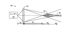
尚、以下の説明で参照する各図面において、類似又は同一の要素を同一の参照符号で示している。図1は、本発明の実施例による光カプラ100のブロックダイアグラムである。光カプラ100は、光源110、レンズ素子120、及び光ファイバ130を含んでいる。尚、この光カプラ100には、従来の光トランスミッタに使用されているものなどのマウント又はパッケージ構造も含まれている(図示されていない)。このマウントにより、後述するように、光源110、レンズ要素120、及び光ファイバ130を適切な向きに保持し、位置決めする。光カプラに適するいくつかの既存のマウント又はパッケージ構造の例としては、「半導体レーザー源からの光ビームをシングルモードの光導波路又はファイバと光学的に接続する光カプラ(Optical Coupler Optically Coupling a Light Beam of a Semiconductor Laser Source with a Single Mode Optical Waveguide or Fiber)」という名称の米国特許第6,112,002号の明細書、「光カプラとその製造方法(Optical Coupler and Method of Producing It)」という名称の米国特許第6,112,001号の明細書、及び「光カプラ(Optical Coupler)」という名称の米国特許第5,680,493号の明細書に開示されている。但し、本発明の実施例は、アライメント公差を緩和して、従来の光カプラやトランスミッタに要求された安定性や精度を有しないようなマウント又はパッケージシステムを使用することが可能であるため、光源110、レンズ素子120、及び光ファイバ130を保持するために用いる光カプラ100の構造は、本発明にとって重要なものではない。
In the drawings referred to in the following description, similar or identical elements are denoted by the same reference numerals. FIG. 1 is a block diagram of an
光源110は、通常、放射光の分布角度が比較的大き端面発光型半導体レーザーなどの装置であるが、垂直空洞面発光レーザー(VCSEL)や発光ダイオード(LED)などのその他の発光装置も使用可能である。更には、光源110は、遠隔地のレーザーやその他の光源から光を導く光ファイバや導波路(図示せず)であってもよい。
The
図1のレンズ素子120は、回折2焦点レンズである。単一の焦点を有する回折レンズ素子の製造技法と構造については周知であり、それらは2焦点回折レンズ120にも使用することができる。図1に示されているように、回折レンズ120は、2焦点レンズを作成するのに必要な形状に形成された(又は、パターン化された)1つの面を有している。尚、回折レンズは、これ以外にも、反対側の面に形状を形成したり、或いは入射光を所望の像面上に回折させるべく作用する開口部を有する不透明なパターンを形成することによって作成することもできる。更に回折レンズのその他の構造としては、電気的にプログラム可能なパターンを有する空間変調器、屈折率分布の傾斜パターンを有するようにドーピングされた基板、又は回折及び屈折機能の組み合わせを有する構造を備えたものが含まれるが、これらに限定されるものではない。
レ ン ズ The
図2は、単色光に対して単一の焦点距離f1を有する従来の回折レンズ200の表面形状を部分的に示している。具体的には、回折レンズ200は、回折レンズ200に平行光束として入射する単色光の回折によって入射光の一部が回折レンズ200の焦点距離f1において集光するよう、間隔と形状が選択されたリッジ部210を有している。一般的に、リッジ部210の高さと形状を調節し、焦点距離f1において集光される入射光のパーセンテージと、集光されることなく回折レンズ200を通過する光のパーセンテージとを設定することができる。
FIG. 2 partially shows the surface shape of a conventional
図3は、2つの焦点距離f1及びf2を提供するリッジ部310を有する面を備えた2焦点回折レンズ300の表面形状を部分的に示している。2焦点回折レンズ300の設計プロセスは、焦点距離f1を有する一般的な回折レンズ200の表面形状を定義する第1位相関数を決定することから始まる。回折レンズ設計用の従来技法を使用することができる。特に、アプライド・オプティクス・リサーチ社(Applied Optics Research, Inc.)のGLADやエムエム・リサーチ社(MM Research, Inc.)のDIFFRACTなどの市販ソフトウェアを使用すれば、回折素子の位相関数を分析することができる。同様に第2位相関数も生成されるが、この第2位相関数は、第1位相関数と組み合わされたときに、その組み合わせが第2の焦点距離f2を有する回折レンズを提供するようになっている。その後、入射光の一定のパーセンテージ(例:50%)を集光させると共に入射光の残り(例:50%)をそのまま通過させる部分的に有効な回折レンズを提供するべく、第2位相関数をスケーリングする。そして、第1位相関数とスケーリングされた第2位相関数を組み合わせ、最終的な2焦点レンズ設計が行われる。
FIG. 3 partially shows a surface shape of a
従来のフォトリソグラフィによるエッチング技法によれば、基板をエッチングし、2焦点回折レンズを形成する所望の表面形状を形成、或いは近似することができる。図1の光カプラ100の実施例においては、光源110は、波長が約1310nmの光を生成し、レンズ素子120は、この1310nmの光に対して透明なシリコンから形成されている。尚、シリコン基板を正確にエッチングする方法は集積回路の製造分野において周知であり、必要に応じて、複数段の段階形状を使用して所望の傾斜形状を近似することができる。
According to a conventional photolithographic etching technique, a substrate can be etched to form or approximate a desired surface shape for forming a bifocal diffraction lens. In the embodiment of the
図4は、光ファイバ130と2焦点レンズ120と間の、軸方向距離DFの関数として、図1の光カプラ100のパワー分布と結合(伝達)効率を示している。例としては、2焦点レンズ120は、約700μmの第1焦点距離f1と1400μmの第2焦点距離f2を有している。光源110は、2焦点レンズ120に対して約200μmの物体距離DOに位置している。この構成により、約5倍の平均倍率と、それに対応して両像面における光の角度分布(ビーム・アングル)の減少が達成できる。
FIG. 4 shows the power distribution and coupling (transmission) efficiency of the
図4の空間150は、許容不能な結合(伝達)効率の変動を引き起こすことなく、光ファイバ130の入射面を配置可能な位置の範囲を表している。この空間150内では、光のパワー分布410は、前方と後方の像面の位置DI1及びDI2(図1参照)でシャープに集光された状態と、前方と後方の像面間で広がった状態との間で変化している。図4のパワー分布410は、少なくとも光ファイバ130への最小限の所望のパワー結合が提供されるしきい値レベルを上回る光の放射照度を含む断面領域を表している。又、好都合なことに、回折レンズ120は、楕円形の分布形状を有するパワー分布410の程度が光源110のオリジナルの光分布と比べて軽度になるよう、光分布のひずみをフィルタ処理(即ち、除去)する。従って、回折レンズ120は、光の楕円形形状の分布を生成する傾向がある端面発光型半導体レーザーなどの光源によって発生する結合(伝達)効率の変動をも軽減している。
4 The
図示されている光軸に沿った分布410の直径は、光ファイバ130の横方向の(即ち、光軸からずれる方向の)ミスアライメント又は動きに対する許容値を示している。更に、プロット420上のエラーバー(誤差指示線)422は、光ファイバ130を軸方向の様々な位置に配置した場合の±5μmの横方向のシフトが結合(伝達)効率に与える影響の大きさを示している。本実施例では、光の分布410の強度は、軸方向に沿う2つの焦点間の範囲425において少なくとも25μmの直径の空間内でゆっくりとした変化を示している。
The diameter of the
このプロット420は、光ファイバ130の入射面の軸方向の位置が光軸上であって且つ範囲425内に存在していれば、結合(伝達)効率の変動が約2デシベル未満であることを示している。範囲425内の公称結合(伝達)効率は約17%であり、従来の突き当て接続技法を使用した場合に実現可能な10%未満の結合(伝達)効率と比べて改善されている。無論、この実施例における光カプラ100の結合(伝達)効率は、光ファイバの入射面上に光をシャープに集束するレンズによって理論的に実現可能な略100%のピーク結合(伝達)効率と比べれば低くなっている。しかしながら、単一のシャープな焦点の場合には、光ファイバの5μmのミスアライメント(又は、シフト)によって結合(伝達)効率が大幅に低下する(例:−7dB)。それに比べ、2焦点レンズ120に対する光ファイバ130のアライメント公差は、従来の光カプラに許容される値の何倍にもなっており、本実施例の場合には、光ファイバ130の5μmのミスアライメント(又は、シフト)による結合(伝達)効率の低下は、わずかに約−0.7dBである。
This
図5は、光源110のミスアライメントが図1に示す実施例光カプラ100の結合(伝達)効率に与える変化を示している。この図5のプロット510は、光源110の軸方向のミスアライメントに対する結合(伝達)効率の依存性を示しており、エラーバー520は、光源110の軸方向の様々な位置でのファイバ130の5μmの横方向のミスアライメントによって発生する結合(伝達)効率の変化を示している。
FIG. 5 shows the change that the misalignment of the
光源110の位置がシフト(即ち、ミスアライメント)すると、通常、光カプラ100の倍率に応じて空間150の位置にも拡大したシフトが発生する。倍率が5倍の場合には、光源110が光軸に対して距離Yだけ横方向にシフト(即ち、ミスアライメント)すると、空間150は約5Yの距離だけ横方向にシフトし、光源110が軸方向に距離Zだけシフト(又は、ミスアライメント)すると、空間150は軸方向に約25Zの距離だけシフトする。この倍率においても、空間150の長さは、光源110の最大5μmの軸方向のミスアライメントによる結合(伝達)効率の変化が約0.7dB未満になるようになっている。光ファイバ130を光源110の位置に対して横方向(光ファイバ130の光軸と直交する方向)にアライメントする能動的なアライメントプロセスによって光源110の横方向の位置の影響を除去することが可能であり、この結果、横方向のミスアライメントによる結合(伝達)効率の変動は光ファイバ130の横方向のアライメント精度によってのみ制限される。従って、能動的な横方向のアライメントプロセスにより、±5μmものアライメント公差を設定しても結合(伝達)効率の変動は約0.7dB未満に収まる。
When the position of the
このようにミスアライメント公差が緩和された結果、単純且つ大量の生産プロセスを使用した光カプラ100の製造が可能となる。特に、光源110、レンズ素子120、及び光学素子130は、それぞれの要素110、120、及び130の相対的な位置を制御するためのアライメントマーク又はその他の可視標識を使用して機械的にアライメントすることができる。この機械的なアライメントの後に、能動的な微調整プロセスにより、光源110を作動させ、光ファイバ130上で伝播する観測光のパワーに基づいて光ファイバ130を横方向にアライメントする。本発明の実施例においては、この能動的なアライメントに要求される精度は、シングルモード光ファイバ用の従来の光カプラのアライメントに必要とされている±1μm以下に対して、±5μm以下にも拡げられる。更に、光ファイバ130の軸方向のアライメントについても、光ファイバに結合された光の放射照度を計測した後にこの計測値に従って光ファイバの軸方向の位置を調節するという時間のかかる能動的なプロセスが不要であり、視覚的な或いは機械的なアライメント技法のみによって実行可能である。
結果 As a result of the reduction of the misalignment tolerance, the
図1に示す例においては、回折2焦点素子120を使用して、照射光の角度が狭められた分布と、光ファイバ130への均一なパワーの結合と、ミスアライメントに対する公差の緩和とを提供する所望の空間150を生成している。しかしながら、その他の光学素子によっても、同様に光源からの光を広げ、ミスアライメントの許容値を緩和することが可能であり、例えば、屈折2焦点又は多焦点レンズによって光源110からの光の放射照度を均一に広げることができる。屈折レンズには、例えば、焦点距離が異なる複数の輪帯状レンズによって取り囲まれた円形のレンズが含まれている。或いはこの代わりに、屈折レンズは、上半分及び下半分に分割したハーフレンズ、或いは(菓子の)パイを放射状に分割したパイピースのような形状(扇形)のレンズ片を組み合わせたものを含んでもよい。但し、様々なレンズセクションからのコヒーレント光間の干渉を考慮し、ミスアライメントの許容値を定義する空間内に許容不能な変動(即ち、明確な干渉の極大と極小)を生成する干渉現象を回避しなければならない。又、光源110から出射される光のパターンのサイズや形状の変動に結合(伝達)効率が依存しないように注意しなければならない。回折レンズの場合には、レンズセクションや領域ごとに異なる焦点を有してはおらず、すべての入射光を均等に広げる望ましい特性を有している。
In the example shown in FIG. 1, a diffractive
図6は、ハイブリッド回折/屈折素子620を有する光カプラ600を示している。このハイブリッド回折/屈折素子620は、光源110からの光を空間150内に広げ、前述のように光ファイバ130に対するアライメント公差を拡大する。一実施例において、ハイブリッド回折/屈折レンズ620は、1つの焦点距離(例:f2)用の曲面622を有する少なくとも1つの表面を備えている。更に、部分的に有効な回折レンズの回折機能624がハイブリッド回折/屈折レンズ620の1つ又は両方の表面に重ね合わせられている。その結果、この組み合わせが入射光の別個の部分に対して2つの焦点距離f1及びf2を提供するようになっている。尚、この図6では、回折機能624が曲面622上に位置しているが、多くのその他の構成が可能であり、例えば、回折及び屈折面が互いに反対側に位置したり、或いは別個の素子である回折素子と屈折素子を組み合わせたりしてハイブリッド回折/屈折2焦点レンズを形成することも可能である。
FIG. 6 shows an
単一チャンネル光カプラ100又は600に示されているものなどの本発明の原理は、マルチチャンネル光トランスミッタ及びカプラに対しても有益である。図7は、本発明の一実施例によるマルチチャンネル光トランスミッタ700を示している。この光トランスミッタ700には、モノリシックダイ上に配置された複数の端面発光型半導体レーザー715を含む一体型アレイ710、複数の2焦点回折レンズ725を含む光ダイ720、及び複数の光ファイバ735を含むファイバアセンブリ730が含まれている。一体型アレイ710及び光ダイ720の製造に使用される半導体プロセス技法により、一体型アレイ710内のレーザー715と光ダイ720内の2焦点回折レンズ725の相対的な位置又はピッチが正確に制御される。或いはこの代わりに、アライメント公差が緩和されたことにより、モノリシックダイ上に複数のコンポーネントを配置するのに代えて、個別のダイを組み立ててマルチチャンネルトランスミッタを形成することも可能である。又、ファイバアセンブリ730用の代表的な構造として、V字型溝の中に光ファイバ735を取り付けるが、このV字型溝は、フォトリソグラフのパターニング及びエッチング或いは精密機械加工により、間隔を正確に制御して基板内に形成することができる。
The principles of the present invention, such as those shown in single-channel
コンポーネント710、720、及び730のアライメントが各チャンネルに提供するのは最善でも平均的なアライメントであり、それぞれのチャンネルに含まれているレーザー715、回折2焦点レンズ725、及び光ファイバ735が最適にはアライメントされないため、複数のレーザー715、レンズ725、及び光ファイバ735をマルチチャンネル光トランスミッタ700内に一体化すると、ミスアライメントが増大する。本発明の一態様によれば、この平均的なアライメントは1つ又は複数のチャンネルにとっては最適なものではないであろうが、アライメント公差を緩和可能な2焦点レンズ725を用いることにより、それぞれのチャンネルは一貫性のある(チャンネル間でばらつきの少ない、あるいは安定した)パワー結合を提供することができる。
The alignment of
以上、特定の実施例を参照して本発明について説明したが、上述の説明は、本発明の一応用例に過ぎず、本発明を限定するものではない。特に、2焦点レンズを含む本発明の模範的な実施例について説明しているが、本発明のその他の実施例においては、3つ以上の焦点距離を備えるマルチ焦点光学系によって同様に光の放射照度を広げ、アライメント公差を緩和することができる。従って、開示した実施例の特徴の様々なその他の適合及び組み合わせも添付の請求項によって定義される本発明の範囲内である。 Although the present invention has been described with reference to the specific embodiments, the above description is merely an application of the present invention and does not limit the present invention. In particular, while an exemplary embodiment of the invention including a bifocal lens is described, in other embodiments of the invention, light emission is likewise achieved by a multifocal optic with three or more focal lengths. Illuminance can be increased and alignment tolerances can be relaxed. Accordingly, various other adaptations and combinations of features of the embodiments disclosed are within the scope of the invention as defined by the appended claims.
なお、本発明は、例として以下の実施態様を含む。
[1] 光源(110)と、前記光源からの光を入射可能な入射面を備える光ファイバ(130)と、前記光源(110)からの光を成形するべく配置され、前記入射面を収容する空間(150)を形成するべく前記空間(150)内に前記光を均一に広げる光学系(120)とを有することを特徴とする装置。
[2] 前記光学系(120)は、前記光源(110)からの光の第1の部分用の第1焦点と前記光源(110)からの光の第2の部分用の第2焦点を備える多焦点レンズ(300)を有することを特徴とする[1]記載の装置。
[3] 前記光学系(120)は、回折レンズ(300)を有することを特徴とする[1]又は[2]に記載の装置。
[4] 前記光学系(120)は、ハイブリッド回折/屈折レンズを有することを特徴とする[1]又は[2]に記載の装置。
[5] 前記光ファイバ(130)は、シングルモード光ファイバであることを特徴とする[1]から[4]のいずれか一つに記載の装置。
[6] 第2光源(715)と、前記第2光源(715)からの光を入射可能な入射面を備える第2光ファイバ(735)と、前記第2光源(715)からの光を成形するべく配置され、前記第2光ファイバ(735)の入射面を収容する第2空間を形成するべく前記第2空間内に前記第2光源からの光を均一に広げる第2光学系(725)とを更に有することを特徴とする[1]から[5]のいずれか一つに記載の装置。
[7] 前記光学系(120)は、前記光源からの光の第1の部分を前記ファイバ(130)の入射面の前方に位置する第1像面上に集束させると共に、前記光の第2部分を前記ファイバ(130)の入射面の後方に位置する第2像面上に集束させることを特徴とする[1]から[6]のいずれか一つに記載の装置。
[8] 光を光ファイバ内に導く方法であって、前記光ファイバ(130)のアライメント精度を上回る寸法を備える空間(150)内に前記光を広げることにより、前記空間のそれぞれの断面において均一で一貫性のある光の放射照度を提供する段階と、前記空間内に前記光ファイバ(130)の入射面を配置する段階とを有することを特徴とする方法。
[9] 前記光を広げる段階は、前記光が2焦点レンズ(300又は620)を通過するように導く段階を有することを特徴とする[8]に記載の方法。
[10] 前記2焦点レンズ(300)は回折レンズを有することを特徴とする[9]に記載の方法。
The present invention includes the following embodiments as examples.
[1] A light source (110), an optical fiber (130) having an incident surface to which light from the light source can enter, and an optical fiber (130) arranged to shape the light from the light source (110) and accommodating the incident surface. An optical system (120) for uniformly spreading the light within the space (150) to form a space (150).
[2] The optical system (120) includes a first focal point for a first part of the light from the light source (110) and a second focal point for a second part of the light from the light source (110). The device according to [1], further comprising a multifocal lens (300).
[3] The device according to [1] or [2], wherein the optical system (120) has a diffractive lens (300).
[4] The apparatus according to [1] or [2], wherein the optical system (120) has a hybrid diffraction / refraction lens.
[5] The apparatus according to any one of [1] to [4], wherein the optical fiber (130) is a single mode optical fiber.
[6] A second light source (715), a second optical fiber (735) having an incident surface capable of receiving light from the second light source (715), and shaping light from the second light source (715) A second optical system (725) for uniformly spreading the light from the second light source in the second space to form a second space for receiving the entrance surface of the second optical fiber (735). The device according to any one of [1] to [5], further comprising:
[7] The optical system (120) focuses a first portion of the light from the light source on a first image plane located in front of an incidence surface of the fiber (130), and further includes a second portion of the light. Apparatus according to any one of [1] to [6], characterized in that the part is focused on a second image plane located behind the plane of incidence of the fiber (130).
[8] A method for guiding light into an optical fiber, wherein the light is spread in a space (150) having a dimension exceeding the alignment accuracy of the optical fiber (130), so that the light is uniform in each cross section of the space. Providing a consistent light irradiance at the same time, and locating the entrance surface of the optical fiber (130) in the space.
[9] The method of [8], wherein spreading the light comprises directing the light to pass through a bifocal lens (300 or 620).
[10] The method according to [9], wherein the bifocal lens (300) has a diffractive lens.
110 光源
120 光学系
130 光ファイバ
150 空間
300 多焦点レンズ
620 ハイブリッド回折/屈折レンズ
715 第2光源
725 第2光学系
735 第2光ファイバ
110
Claims (1)
前記光源からの光を入射可能な入射面を備える光ファイバと、
前記光源からの光を成形するべく配置され、前記入射面を収容する空間を形成するべく前記空間内に前記光源からの光を均一に広げる光学系と、
を有することを特徴とする装置。 A light source,
An optical fiber having an incident surface capable of receiving light from the light source,
An optical system that is arranged to shape light from the light source and uniformly spreads light from the light source in the space to form a space that houses the incident surface;
An apparatus comprising:
Applications Claiming Priority (1)
| Application Number | Priority Date | Filing Date | Title |
|---|---|---|---|
| US10/210,598 US6956992B2 (en) | 2002-07-31 | 2002-07-31 | Optical fiber coupler having a relaxed alignment tolerance |
Publications (2)
| Publication Number | Publication Date |
|---|---|
| JP2004070339A true JP2004070339A (en) | 2004-03-04 |
| JP2004070339A5 JP2004070339A5 (en) | 2006-08-31 |
Family
ID=27804777
Family Applications (1)
| Application Number | Title | Priority Date | Filing Date |
|---|---|---|---|
| JP2003273500A Withdrawn JP2004070339A (en) | 2002-07-31 | 2003-07-11 | Optical fiber coupler for relieving alignment tolerance |
Country Status (4)
| Country | Link |
|---|---|
| US (2) | US6956992B2 (en) |
| JP (1) | JP2004070339A (en) |
| DE (1) | DE10320152B4 (en) |
| GB (1) | GB2392993B (en) |
Cited By (2)
| Publication number | Priority date | Publication date | Assignee | Title |
|---|---|---|---|---|
| JP2009258154A (en) * | 2008-04-11 | 2009-11-05 | Sumitomo Electric Ind Ltd | Optical transmission module and manufacturing method therefor |
| JP2010530715A (en) * | 2007-06-18 | 2010-09-09 | ヒューレット−パッカード デベロップメント カンパニー エル.ピー. | Misalignment-resistant free-space optical transceiver |
Families Citing this family (16)
| Publication number | Priority date | Publication date | Assignee | Title |
|---|---|---|---|---|
| US7343535B2 (en) * | 2002-02-06 | 2008-03-11 | Avago Technologies General Ip Dte Ltd | Embedded testing capability for integrated serializer/deserializers |
| US6956992B2 (en) * | 2002-07-31 | 2005-10-18 | Agilent Technologies, Inc. | Optical fiber coupler having a relaxed alignment tolerance |
| WO2004077119A1 (en) * | 2003-02-25 | 2004-09-10 | Digital Optics Corporation | Diffractive coupler optimized for alignment tolerances |
| US20050063431A1 (en) * | 2003-09-19 | 2005-03-24 | Gallup Kendra J. | Integrated optics and electronics |
| US7520679B2 (en) * | 2003-09-19 | 2009-04-21 | Avago Technologies Fiber Ip (Singapore) Pte. Ltd. | Optical device package with turning mirror and alignment post |
| US6953990B2 (en) * | 2003-09-19 | 2005-10-11 | Agilent Technologies, Inc. | Wafer-level packaging of optoelectronic devices |
| JP2005175842A (en) * | 2003-12-10 | 2005-06-30 | Canon Inc | Photodetector and optical space transmission apparatus |
| US20050213995A1 (en) * | 2004-03-26 | 2005-09-29 | Myunghee Lee | Low power and low jitter optical receiver for fiber optic communication link |
| US6975784B1 (en) * | 2004-09-10 | 2005-12-13 | Intel Corporation | Singulated dies in a parallel optics module |
| US20080170826A1 (en) * | 2007-01-16 | 2008-07-17 | Applied Optical Materials | Misalignment-tolerant optical coupler/connector |
| US20120294568A1 (en) * | 2011-05-18 | 2012-11-22 | Agency For Science, Technology And Research | Alignment Method for a Silicon Photonics Packaging |
| US8714834B2 (en) * | 2011-11-30 | 2014-05-06 | The United States Of America As Represented By The Secretary Of The Navy | Multichannel optical data coupler |
| US9946040B2 (en) * | 2014-01-17 | 2018-04-17 | Empire Technology Development Llc | Optical fibers without cladding |
| US9453967B2 (en) | 2014-10-17 | 2016-09-27 | Lumentum Operations Llc | High power misalignment-tolerant fiber assembly |
| WO2016187330A1 (en) * | 2015-05-18 | 2016-11-24 | Lasermotive, Inc. | Diffusion safety system |
| US11480495B2 (en) * | 2017-08-07 | 2022-10-25 | Jenoptik Optical Systems Gmbh | Position-tolerance-insensitive contacting module for contacting optoelectronic chips |
Family Cites Families (27)
| Publication number | Priority date | Publication date | Assignee | Title |
|---|---|---|---|---|
| US4732448A (en) | 1984-12-07 | 1988-03-22 | Advanced Interventional Systems, Inc. | Delivery system for high-energy pulsed ultraviolet laser light |
| JP2508219B2 (en) * | 1988-10-11 | 1996-06-19 | 日本電気株式会社 | Semiconductor laser module |
| JPH04273206A (en) * | 1991-02-28 | 1992-09-29 | Nec Corp | Semiconductor laser array module |
| US5370643A (en) | 1992-07-06 | 1994-12-06 | Ceramoptec, Inc. | Multiple effect laser delivery device and system for medical procedures |
| JP2839807B2 (en) | 1992-10-02 | 1998-12-16 | アルプス電気株式会社 | Assembly method of optical coupling device |
| US5555333A (en) * | 1993-07-12 | 1996-09-10 | Ricoh Company, Ltd. | Optical module and a fabrication process thereof |
| JP3282889B2 (en) | 1993-08-04 | 2002-05-20 | 古河電気工業株式会社 | Optical fiber with lens |
| GB9407893D0 (en) | 1994-04-21 | 1994-06-15 | British Nuclear Fuels Plc | Radiation coupling arrangements |
| US5606434A (en) | 1994-06-30 | 1997-02-25 | University Of North Carolina | Achromatic optical system including diffractive optical element |
| US5511140A (en) | 1994-10-13 | 1996-04-23 | International Business Machines Corporation | Molded plastic optical fiber-optoelectronic converter subassembly |
| US5557693A (en) * | 1994-10-21 | 1996-09-17 | Unisys Corporation | Apparatus and method for transmitting optical data |
| JPH08338927A (en) | 1995-06-13 | 1996-12-24 | Oki Electric Ind Co Ltd | Optical coupler and its assembling method |
| JP3472660B2 (en) * | 1995-06-22 | 2003-12-02 | 日本オプネクスト株式会社 | Optical semiconductor array module, assembling method thereof, and external substrate mounting structure |
| US5687264A (en) * | 1995-08-24 | 1997-11-11 | Sandia Corporation | Apparatus for injecting high power laser light into a fiber optic cable |
| US5744239A (en) * | 1996-09-27 | 1998-04-28 | Minnesota Mining And Manufacturing Company | Addition of antimicrobial agents to pavement marking materials |
| US5892866A (en) * | 1996-10-01 | 1999-04-06 | Honeywell Inc. | Fiber optic mode scrambler |
| US6112002A (en) | 1996-11-29 | 2000-08-29 | Fujitsu Limited | Optical coupler optically coupling a light beam of a semiconductor laser source with a single mode optical waveguide or fiber |
| GB9703156D0 (en) * | 1997-02-15 | 1997-04-02 | Univ Strathclyde | Optical element |
| US6120191A (en) | 1997-02-26 | 2000-09-19 | Matsushita Electric Industrial Co., Ltd. | Laser diode module |
| JP3792358B2 (en) | 1997-07-30 | 2006-07-05 | 京セラ株式会社 | Optical connection component and manufacturing method thereof |
| KR100450577B1 (en) * | 1998-09-17 | 2004-09-30 | 마쯔시다덴기산교 가부시키가이샤 | Coupling lens and semiconductor laser module |
| US6272269B1 (en) * | 1999-11-16 | 2001-08-07 | Dn Labs Inc. | Optical fiber/waveguide illumination system |
| CN1311566C (en) * | 1999-11-30 | 2007-04-18 | 欧姆龙株式会社 | Optical device and apparatus comprising said optical device |
| US6511140B2 (en) * | 2000-06-06 | 2003-01-28 | Fulterer Gesellschaft M.B.H. | Pull-out device for a tall cupboard drawer |
| DE10056861C1 (en) * | 2000-11-16 | 2002-08-08 | Siemens Ag | Mode exciting device for optical waveguide, uses reflector that deflects reflected edge beam of coherent beam onto entry face onto which edge beams of coherent beam are directed |
| US6822794B2 (en) | 2000-12-15 | 2004-11-23 | Agilent Technologies, Inc. | Diffractive optical element for providing favorable multi-mode fiber launch and reflection management |
| US6956992B2 (en) * | 2002-07-31 | 2005-10-18 | Agilent Technologies, Inc. | Optical fiber coupler having a relaxed alignment tolerance |
-
2002
- 2002-07-31 US US10/210,598 patent/US6956992B2/en not_active Expired - Lifetime
-
2003
- 2003-05-06 DE DE10320152A patent/DE10320152B4/en not_active Expired - Fee Related
- 2003-07-11 JP JP2003273500A patent/JP2004070339A/en not_active Withdrawn
- 2003-07-29 GB GB0317738A patent/GB2392993B/en not_active Expired - Fee Related
-
2005
- 2005-06-17 US US11/155,156 patent/US7308170B2/en not_active Expired - Lifetime
Cited By (3)
| Publication number | Priority date | Publication date | Assignee | Title |
|---|---|---|---|---|
| JP2010530715A (en) * | 2007-06-18 | 2010-09-09 | ヒューレット−パッカード デベロップメント カンパニー エル.ピー. | Misalignment-resistant free-space optical transceiver |
| US8315526B2 (en) | 2007-06-18 | 2012-11-20 | Hewlett-Packard Development Company, L.P. | Misalignment tolerant free space optical transceiver |
| JP2009258154A (en) * | 2008-04-11 | 2009-11-05 | Sumitomo Electric Ind Ltd | Optical transmission module and manufacturing method therefor |
Also Published As
| Publication number | Publication date |
|---|---|
| US6956992B2 (en) | 2005-10-18 |
| DE10320152B4 (en) | 2006-07-13 |
| GB0317738D0 (en) | 2003-09-03 |
| DE10320152A1 (en) | 2004-02-26 |
| US20050259918A1 (en) | 2005-11-24 |
| GB2392993B (en) | 2005-07-06 |
| US7308170B2 (en) | 2007-12-11 |
| GB2392993A (en) | 2004-03-17 |
| US20040022488A1 (en) | 2004-02-05 |
Similar Documents
| Publication | Publication Date | Title |
|---|---|---|
| US7308170B2 (en) | Optical fiber coupler having a relaxed alignment tolerance | |
| JP3886542B2 (en) | Fiber integrated microlens, fiber optic Bragg grating coupler, and spectrometer and multiplexer formed thereby | |
| JP2022180575A (en) | Optical system manufacturing method and optical system | |
| US7920763B1 (en) | Mode field expanded fiber collimator | |
| EP1033597A1 (en) | Coupling lens and semiconductor laser module | |
| KR101416792B1 (en) | Optical element for free-space propagation between an optical waveguide and another optical waveguide, component, or device | |
| US4830453A (en) | Device for optically coupling a radiation source to an optical transmission fiber | |
| US6606432B2 (en) | Phase mask consisting of an array of multiple diffractive elements for simultaneous accurate fabrication of large arrays of optical couplers and method for making same | |
| JP2004053992A (en) | Diffraction grating, wavelength multiplexer/demultiplexer and wavelength multiplex signal optical transmission module using them | |
| JP2004279618A (en) | Optical collimator structure | |
| US6625353B2 (en) | Optical module, alignment method of optical module, and alignment device of optical module | |
| JP5725176B2 (en) | Light guide device and light guide method | |
| WO2012118021A1 (en) | Optical waveguide, laser light irradiation device, and method for assembling laser light irradiation device | |
| JP2008203598A (en) | Laser beam condensing unit | |
| US6870195B2 (en) | Array of discretely formed optical signal emitters for multi-channel communication | |
| JP6714555B2 (en) | Optical waveguide component, core alignment method, and optical element mounting method | |
| CN115413326A (en) | Optical coupling and mode selective splitting or superimposing of optical fields | |
| JP2017134228A (en) | Optical waveguide | |
| GB2338569A (en) | Fixing plate for optic fibres and lens array | |
| JPS5973712A (en) | Flatness measuring device | |
| WO1998047032A2 (en) | Optical transmission systems including optical rods with three-dimensional patterns thereon and related structures | |
| KR100968942B1 (en) | Apparatus for locking optical fiber | |
| TW200408841A (en) | Optical waveguide apparatus | |
| JPS6049882B2 (en) | Optical multiplexing/demultiplexing circuit for optical beams | |
| JP4696521B2 (en) | Demultiplexer, optical waveguide, and wavelength division multiplexing optical transmission module |
Legal Events
| Date | Code | Title | Description |
|---|---|---|---|
| A521 | Written amendment |
Free format text: JAPANESE INTERMEDIATE CODE: A523 Effective date: 20060710 |
|
| A621 | Written request for application examination |
Free format text: JAPANESE INTERMEDIATE CODE: A621 Effective date: 20060710 |
|
| A711 | Notification of change in applicant |
Free format text: JAPANESE INTERMEDIATE CODE: A711 Effective date: 20070320 |
|
| RD03 | Notification of appointment of power of attorney |
Free format text: JAPANESE INTERMEDIATE CODE: A7423 Effective date: 20070411 |
|
| A761 | Written withdrawal of application |
Free format text: JAPANESE INTERMEDIATE CODE: A761 Effective date: 20070501 |