JP2004040768A - Lumped constant element hybrid circuit - Google Patents
Lumped constant element hybrid circuit Download PDFInfo
- Publication number
- JP2004040768A JP2004040768A JP2003099547A JP2003099547A JP2004040768A JP 2004040768 A JP2004040768 A JP 2004040768A JP 2003099547 A JP2003099547 A JP 2003099547A JP 2003099547 A JP2003099547 A JP 2003099547A JP 2004040768 A JP2004040768 A JP 2004040768A
- Authority
- JP
- Japan
- Prior art keywords
- inductor
- hybrid
- capacitor
- winding
- balun
- Prior art date
- Legal status (The legal status is an assumption and is not a legal conclusion. Google has not performed a legal analysis and makes no representation as to the accuracy of the status listed.)
- Pending
Links
- 239000003990 capacitor Substances 0.000 claims abstract description 86
- 239000000758 substrate Substances 0.000 claims abstract description 34
- 238000004804 winding Methods 0.000 claims description 50
- 230000000903 blocking effect Effects 0.000 claims description 10
- 238000001465 metallisation Methods 0.000 abstract description 13
- 238000013461 design Methods 0.000 abstract description 12
- 239000002184 metal Substances 0.000 description 14
- 230000008878 coupling Effects 0.000 description 11
- 238000010168 coupling process Methods 0.000 description 11
- 238000005859 coupling reaction Methods 0.000 description 11
- 238000004891 communication Methods 0.000 description 10
- 230000008901 benefit Effects 0.000 description 4
- 238000010586 diagram Methods 0.000 description 4
- 230000003071 parasitic effect Effects 0.000 description 4
- 230000009977 dual effect Effects 0.000 description 3
- 238000000059 patterning Methods 0.000 description 2
- 230000010363 phase shift Effects 0.000 description 2
- 229910001218 Gallium arsenide Inorganic materials 0.000 description 1
- 230000005540 biological transmission Effects 0.000 description 1
- 230000001934 delay Effects 0.000 description 1
- 238000005137 deposition process Methods 0.000 description 1
- 238000010292 electrical insulation Methods 0.000 description 1
- 230000001939 inductive effect Effects 0.000 description 1
- 239000000463 material Substances 0.000 description 1
- 238000000034 method Methods 0.000 description 1
- 238000012986 modification Methods 0.000 description 1
- 230000004048 modification Effects 0.000 description 1
- 235000014366 other mixer Nutrition 0.000 description 1
- 238000012545 processing Methods 0.000 description 1
- 230000001902 propagating effect Effects 0.000 description 1
- 230000004044 response Effects 0.000 description 1
- 229910052594 sapphire Inorganic materials 0.000 description 1
- 239000010980 sapphire Substances 0.000 description 1
Images
Classifications
-
- H—ELECTRICITY
- H04—ELECTRIC COMMUNICATION TECHNIQUE
- H04B—TRANSMISSION
- H04B1/00—Details of transmission systems, not covered by a single one of groups H04B3/00 - H04B13/00; Details of transmission systems not characterised by the medium used for transmission
- H04B1/38—Transceivers, i.e. devices in which transmitter and receiver form a structural unit and in which at least one part is used for functions of transmitting and receiving
- H04B1/40—Circuits
- H04B1/50—Circuits using different frequencies for the two directions of communication
- H04B1/52—Hybrid arrangements, i.e. arrangements for transition from single-path two-direction transmission to single-direction transmission on each of two paths or vice versa
-
- H—ELECTRICITY
- H03—ELECTRONIC CIRCUITRY
- H03H—IMPEDANCE NETWORKS, e.g. RESONANT CIRCUITS; RESONATORS
- H03H7/00—Multiple-port networks comprising only passive electrical elements as network components
- H03H7/42—Networks for transforming balanced signals into unbalanced signals and vice versa, e.g. baluns
Landscapes
- Engineering & Computer Science (AREA)
- Computer Networks & Wireless Communication (AREA)
- Signal Processing (AREA)
- Semiconductor Integrated Circuits (AREA)
- Coils Or Transformers For Communication (AREA)
Abstract
Description
【0001】
【発明の属する技術分野】
本発明は、一般に、リング・ミクサ用の集中定数素子バランに関し、より詳細には、空間を節約して使い、寄生インダクタンスを最小限に抑える形で、バラン回路素子がモノリシック基板上に構成された集中定数素子リング・バランの回路レイアウトに関する。
【0002】
【従来の技術】
近代の通信システムは、様々な通信チャネルに関連付けられた割当て周波数帯域幅を、最大限に利用しようと試みる送信器設計および受信器設計を使用している。なぜならば、システムの提供者にとって信号の帯域幅は、コストのかかる投資となるためである。割当て帯域幅を最大限に利用することは、極めて高性能の送信器および受信器を提供することになる。しかし、送信器と受信器は、低コストでなければならない。通信システムにおける無線周波数(RF)装置は、一般的に注文設計素子であり、大量生産されないため、通常、最も費用のかかる物品になっている。
【0003】
このカテゴリの範疇であるRF装置の1つは、周波数ミクサである。周波数ミクサは、2つのRF周波数信号又は2つの中間周波数(IF)信号を混合し、和周波数及び差周波数を生成して、周波数をダウン変換し、あるいはアップ変換する。例えば、受信器内で受信される信号は、局部発振器(LO)信号と混合され、後続する信号処理に適したIF信号が、生成される。通常、ミクサは、RF信号チェインの性能を設定するためには不可欠である。したがって、RF集積回路(IC)内のセルとして具体化することができる、相互変調積がより小さく、かつ、ダイナミックレンジの広いミクサが、必要とされる。
【0004】
本明細書において考察するタイプのRF通信システムに使用されている周知のミクサの1つは、当分野でリング・ミクサ(ring mixer)と呼ばれている。リング・ミクサは、リング構成で接続され、IF信号を生成するためのRF信号及びLO信号を混合する4つのダイオードを、採用している。このリング・ミクサは、RF信号およびLO信号を、互いに180°位相がずれた信号に分割するハイブリッド又はバランを、採用している。リング・ミクサ・バランは、Sturdivant,Rick,“Balun Designs for Wireless,...Mixers,Amplifiers and Antennas,”Applied Microwave,Summer 1993,pps.34−44に、開示されている。分割されたRF信号およびLO信号は、リングの対向するコーナにおけるダイオード間のミクサに、印加される。ダイオードは、変調を行うために、RF信号の正の部分および負の部分に応答して、スイッチオンおよびスイッチオフされる。IF信号は、リングのもう一方の対向するコーナのダイオード間で生成される。
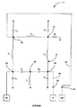
【0005】
図1は、既知の集中定数素子リング・バラン回路10の略図を示したものである。リング・バラン回路10は、コーナ・ノード14、16、18および20を画定している4つの辺を有する電気リング12を備えている。リング・バラン回路10は、コンデンサ(容量子)C1〜C6、インダクタ(誘導子)L1〜L4、および抵抗R1からなる電気的な構成を備えている。リング12の各辺は、伝搬する信号を遅延させる集中定数素子伝送線路を形成する高域通過フィルタを提供するように結合するコンデンサ及びインダクタを備えている。当分野で知られているように、コンデンサ上で電流が電圧を導き、インダクタ上で電圧が電流を導く。したがって、直列コンデンサおよびシャント・インダクタは、信号の位相を進ませ、また、直列インダクタおよびシャント・コンデンサは、信号の位相を遅らせる。
【0006】
RF入力信号は、ノード14にRFに印加され、フィルタは、ノード14における信号に対して位相が90°ずれたノード20におけるRF信号を提供し、また、ノード14における信号に対して位相が180°ずれたノード18におけるRF信号を提供し、さらに、ノード14における信号に対して位相が270°ずれたノード16におけるRF信号を提供する。出力線路54および56が、それぞれ、ノード20および16と結合し、互いに位相が180°ずれた出力信号が、提供される。直流阻止コンデンサ24および26は、出力線路54および56中に設けられ、リング・バラン回路10へのミクサからの直流信号の進入を防止している。
【0007】
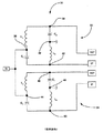
リング・バラン回路10をリング・ミクサに適用することはできるが、二重バランのリング設計は複雑であるため、例えば、星形ミクサ、ダブル・ダブリ平衡ミクサなどの他のタイプのミクサへの使用には限界がある。したがって、当分野において、他のバラン設計が、他のタイプのミクサに使用されている。図2は、集中定数素子二重バラン回路30の略図を示し、その集中定数素子二重バラン回路30は、星形ミクサまたはモノリシック・マイクロ波集積回路(MMIC:Monolithic Microwave Integrated Circuit)ダブル・ダブリ平衡ミクサ(DDBM:Double Doubly Balanced Mixer)と組み合わせて使用するための特定の用途を有する第1バラン32及び第2バラン34を備えている。二重バラン回路30は、RF入力信号を受信し、第1のバラン32は、互いに180°位相がずれた2つの信号を出力し、第2のバラン34は、互いに180°位相がずれた2つのRF信号を出力している。このタイプの二重バラン構造は、Chiou,Hwann−Keo,et al.,“Miniature MMIC Star Double Balanced Mixer Using Lumped Dual Balun,”Electronics Letters,Vol.33,No.6,March 13,1997,pps.503−505、およびChiou,Hwann−Keo,et al.,“A Miniature MMICDouble Doubly Balanced Mixer Using Lumped Dual Balun for High Dynamic Receiver Application,”IEEE,Microwave and Guided Wave Letters,Vol.7,No.8,August 1997,pps.227−229に、開示されている。
【0008】
二重バラン回路30は、上で考察したバラン回路10と同様に、互いに180°位相がずれたRF信号を提供するために、インダクタおよびコンデンサ・フィルタ回路網を採用する。バラン32は、インダクタL1およびコンデンサC1からなるフィルタと、インダクタL2およびコンデンサC2からなるフィルタと、を備えている。同様に、バラン34は、インダクタL3およびコンデンサC3からなるフィルタと、インダクタL4およびコンデンサC4からなるフィルタと、を備えている。バラン32において、インダクタL1は、ノード36でコンデンサC1と結合し、インダクタL1は、ノード38でコンデンサC2と結合している。そのコンデンサC2は、ノード40でインダクタL2と結合し、インダクタL2は、ノード42でコンデンサC1と結合している。バラン34において、インダクタL3は、ノード44でコンデンサC3と結合し、インダクタL3は、ノード46でコンデンサC4と結合している。そのコンデンサC4は、ノード48でインダクタL4と結合し、インダクタL4は、ノード50でコンデンサC3と結合している。RF入力信号は、ノード36および44に印加されている。RF入力信号と同相のRF出力信号は、ノード42および50に提供され、そのRF入力信号に対して180°位相がずれたRF出力信号は、ノード38および46に提供されている。
【0009】
【非特許文献1】
スターディバント・リック(Sturdivant,Rick)著、「ワイヤレス、・・・、ミクサ、アンプ及びアンテナ用のバラン設計(Balun Designs for Wireless,...Mixers,Amplifiers and Antennas)」、応用マイクロ派(Applied Microwave)、1993年 夏(Summer 1993)、p.34−44
【非特許文献2】
キオス・ホアン・キオ(Chiou,Hwann−Keo)ら著、「集中定数二重バランを用いる小型MMIC星形タブル平衡ミクサ(Miniature MMIC Star Double Balanced Mixer Using Lumped Dual Balun)」、エレクトロニクス・レター(Electronics Letters)、第33巻、第6号、1997年3月13日、p.503−505
【非特許文献3】
キオス・ホアン・キオ(Chiou,Hwann−Keo)ら著、「高動力受信用途用の集中定数二重バランを用いる小型MMICダブル・ダブリ平衡ミクサ(A Miniature MMIC Double Doubly Balanced Mixer Using Lumped Dual Balun for High Dynamic Receiver Application)」、IEEE、マイクロ波&誘導波レター(Microwave and Guided Wave Letters)、第7巻、第8号、1997年8月、p.227−229
【0010】
【発明の概要】
本発明の教示によれば、集中定数素子リング・バランのための回路レイアウトが開示され、そこでは、バランの素子が、コンパクトな設計でモノリシック基板上にパターン化される。バランは、RF入力信号をフィルタリングし、かつ、遅延させるために、一体に電気結合された4つのインダクタおよび複数のコンデンサを備えており、それにより、対応する互いに位相がずれたRF出力信号が提供される。インダクタは、基板上の矩形領域に、対称配置される。インダクタの第1の対は、矩形領域の一方の端部に、互いに隣り合って配置される。インダクタの第2の対は、矩形領域の対向する端部に、互いに隣り合って配置される。コンデンサはすべて、インダクタの第1対と第2対との間の中央回路領域の基板上に形成される。
【0011】
設計には、基板上にパターン化された金属化トレースが使用され、インダクタとコンデンサの間の電気結合を提供している。また、トレースは、基板中に異なるレベルで提供されている。インダクタの各々は、回路領域中の回路素子と電気結合された、内側端および外側端を有する巻線を、備えている。各巻線の内側端は、巻線から電気的に分離しているエアブリッジを貫通して巻線の下側に延びるトレースと結合している。寄生インダクタンスを小さくするために、コンデンサまでの電気接続の長さは、最短化されている。接地ビアは、基板を貫通して延び、その基板の反対側で、金属化接地平面に電気接続されている。
【0012】
本発明の他の目的、利点および特徴については、添付の図面と共に、以下の詳細説明および特許請求の範囲の各請求項から明らかになるであろう。
【0013】
【発明の実施の形態】
モノリシック基板上のバランの専用回路レイアウトを対象とした本発明についての以下の考察は、単に例示的な性質のものに過ぎず、本発明またはその用途ないし用法を、何ら限定するものではない。
【0014】
本発明により、空間を節約して使い、寄生キャパシタンスおよび寄生インダクタンスを小さくし、消費電力が少なく、かつ、低コストである、モノリシック基板上のバラン回路10および二重バラン回路30に関する誘導素子および容量素子の配列が提供される。バラン回路10は、リング・ミクサとの使用を意図したものであり、二重バラン回路30は、星形ミクサまたはDDBMとの使用を意図したものである。しかしながら、これは、何ら制限されることのない実施例であり、以下で考察する本発明のバラン構成は、他のシステム(他のミクサ、増幅器、アンテナ等を含む)に対する用途を有している。さらに、本発明は、180°の位相ずれ以外の他の位相ずれの信号を提供するように、構成することもできる。また、このレイアウト設計を、他のタイプの回路(例えば、集積回路基板上の集積回路など)に使用することもできる。
【0015】
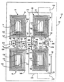
図3は、上で考察したバラン回路10と同じ電気素子を備えたリング・バラン60の回路レイアウトの平面図を示したものである。電気素子は、素子を画定するための導電領域および誘電領域を提供する適切な任意の金属化プロセスおよび蒸着プロセスによって、モノリシック基板62(例えば、MMICなど)上にパターン化されている。基板62は、適切な任意の材料とすることができ、例えば、InP、GaAs、サファイア等である。以下で考察される、トレース中の矩形領域および金属化領域は、電気結合を提供するための垂直拡張領域または重畳金属領域を表している。インダクタを、モノリシック基板上に金属化トレースまたは巻線としてパターン化するため、及び、コンデンサを、対向するプレートを有し、かつ、その間に誘電体が形成された金属化パッチとしてパターン化するための、多くの技法が知られている。本発明は、基板62上のインダクタおよびコンデンサの配置を対象としたものである。この点に関して、バラン60の様々な電気素子を、図1に示す電気素子の簡易表現を参照して考察する。
【0016】
バラン60は、対称に配置されたインダクタを備えており、それらのインダクタは、インダクタL1を表す第1のインダクタ64と、インダクタL2を表す第2のインダクタ66と、インダクタL3を表す第3のインダクタ68と、インダクタL4を表す第4のインダクタ70と、を備える。以下で考察するように、様々なコンデンサC1〜C6と、そのコンデンサC1〜C6とインダクタL1〜L4との間の相互接続とは、中央回路領域72内に提供されており、その中央回路領域72は、インダクタ64および66の対とインダクタ68および70の対との間に画定されている。この方法でインダクタ64〜70を基板62上に対称に配置し、かつ、他の回路素子をその間の中央位置に閉じ込めることにより、バラン60に必要な空間を制限する際に、大きな利点が提供される。
【0017】
インダクタ64は、内側端76および外側端78を有する巻線74を画定している金属化トレースを備えている。インダクタ66は、内側端92および外側端94を有する巻線90を画定している金属化トレースを備えている。インダクタ68は、内側端98および外側端100を有する巻線96を画定している金属化トレースを備えている。インダクタ70は、内側端106および外側端108を有する巻線104を画定している金属化トレースを備えている。インダクタ64〜70は、矩形の態様で示されているが、本発明の範囲に合致する他の設計は、例えば、六角形、円形、楕円形等を始めとする他の形状を含む。
【0018】
内側端76、92、98および106の各々は、回路領域72内の回路素子と電気結合している。必要な電気絶縁を伴うこの電気結合を提供するために、エアブリッジが、巻線74、90、96および104の一部分の真下に形成されている。このエアブリッジは、巻線の隆起部分によって形成され、その結果、巻線が、トレースと電気接続することなく、かつ、最小の電気結合を有する。本明細書において考察するように、相互接続ビアは、2つのトレースを電気接続させるための金属化領域であるか、あるいは2つのトレースがオーバラップした領域である。
【0019】
巻線74の端部76は、相互接続ビア122によって、金属トレース120と電気結合している。トレース120は、巻線74から電気絶縁されており、巻線74によって形成されたエアブリッジ124を貫通して延びており、相互接続ビア128によって、ノード14を画定している金属化領域130と結合している。巻線90の端部92は、相互接続ビア138によって、金属トレース136と電気結合している。トレース136は、巻線90から電気絶縁されており、巻線90によって形成されたエアブリッジ140を貫通して延びており、相互接続ビア142によって、ノード18を画定している金属化領域144と結合している。巻線96の端部98は、相互接続ビア152によって、金属トレース150と電気結合している。トレース150は、巻線96から電気絶縁されており、巻線96によって形成されたエアブリッジ154を貫通して延びており、相互接続ビア156によって、同様にノード18を表す金属化領域158と結合している。巻線104の端部106は、相互接続ビア172によって、金属トレース170と電気結合している。トレース170は、巻線104から電気絶縁されており、巻線104によって形成されたエアブリッジ174を貫通して延びており、相互接続ビア176によって金属化領域182と結合している。
【0020】
コンデンサC1を表すコンデンサ190の頂部プレートは、金属化領域130と電気結合し、コンデンサ190の底部プレートは、接地ビア180と結合している。接地ビア180は、基板62を貫通して延びており、基板62の反対側の表面上の金属化接地平面(図示せず)と電気結合している。接地ビア180は、モノリシック基板62上の頂部表面の接地パッチとして作用する金属化領域178と電気結合している。金属化領域178は、金属化領域182と結合し、それにより、巻線104の端部106が接地と結合している。
【0021】
コンデンサC6を表すコンデンサ192の頂部プレートは、金属化領域130と電気結合し、それにより、インダクタ64とコンデンサ192が電気結合している。コンデンサ192の底部プレートは、ノード22を表す金属化領域194と電気結合している。コンデンサC5を表すコンデンサ198の頂部プレートは、金属化領域194と電気結合し、かつ、巻線104の端部108と電気結合している。コンデンサ198の底部プレートは、巻線96の端部100と電気結合し、かつ、ノード20を表す金属化領域200と電気結合している。コンデンサC4を表すコンデンサ202の頂部プレートは、金属化領域200と電気結合し、コンデンサ202の底部プレートは、金属化領域206と電気結合している。コンデンサC2を表すコンデンサ226の底部プレートも、金属化領域206と電気結合している。コンデンサ226の頂部プレートは、巻線74の端部78および巻線90の端部94と電気結合している。この接続ポイントは、ノード16を表している。
【0022】
モノリシック基板62の頂部表面の金属化領域210は、接地平面と電気結合した接地ビア208と電気結合している。また、金属化領域206も、接地ビア208と電気結合している。コンデンサC3を表すコンデンサ214の底部プレートは、金属化領域210と電気結合している。コンデンサ214の頂部プレートは、金属化領域144および158と電気結合し、インダクタ66および68をコンデンサ214に結合している。また、コンデンサ214の頂部プレートは、抵抗R1を表す金属化領域216と結合している。この金属化領域216は、接地ビア220と電気結合した金属化領域218と結合している。接地ビア220は、モノリシック基板62を貫通して延び、接地平面と電気結合している。
【0023】
ノード14に印加されるRF入力信号は、金属化領域230に印加される。金属化領域230は、コンデンサ190の頂部プレートと電気結合している。180°位相出力トレース232は、コンデンサ226の頂部プレートと電気結合し、図に示すようにインダクタ64と66との間を延びている。コンデンサ24を表す直流阻止コンデンサ234は、出力トレース232と結合している。ゼロ位相出力トレース236は、コンデンサ198の頂部プレートと電気結合し、図に示すようにインダクタ68と70との間を延びている。直流阻止コンデンサ238は、出力トレース236と結合している。
【0024】
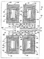
図4は、図2に示す二重バラン回路30と同じ素子を備えた二重バラン248の回路レイアウトの平面図を示したものである。二重バラン248の素子は、モノリシック基板250上に形成されている。二重バラン248は、インダクタL1を表す第1のインダクタ252と、インダクタL2を表す第2のインダクタ254と、インダクタL3を表す第3のインダクタ256と、インダクタL4を表す第4のインダクタ258とを備えている。以下で考察するように、様々なコンデンサC1〜C4と、そのコンデンサC1〜C4とインダクタL1〜L4との間の相互接続とが、インダクタ252および254の対とインダクタ256および258の対との間に画定された中央回路領域260内に提供されている。
【0025】
インダクタ252は、内側端264および外側端266を有する巻線262を画定している金属化トレースを備えている。内側端264は、相互接続ビア270によって、金属トレース268と電気結合している。金属トレース268は、巻線262によって形成されたエアブリッジ274を貫通して延びており、相互接続ビア276と電気結合している。相互接続ビア276は、ノード36を表す金属化領域278と電気結合している。
【0026】
インダクタ254は、内側端284および外側端286を有する巻線282を画定している金属化トレースを備えている。内側端284は、相互接続ビア290によって、金属トレース288と電気結合している。金属トレース288は、巻線282によって形成されたエアブリッジ292を貫通して延びており、相互接続ビア294と電気結合している。相互接続ビア294は、ノード40を表す金属化領域296と電気結合している。
【0027】
インダクタ256は、内側端302および外側端304を有する巻線300を画定している金属化トレースを備えている。内側端302は、相互接続ビア308によって、金属トレース306と電気結合している。金属トレース306は、巻線300によって形成されたエアブリッジ310を貫通して延びており、相互接続ビア312と電気結合している。相互接続ビア312は、ノード44を表す金属化領域314と電気結合している。
【0028】
インダクタ258は、内側端322および外側端324を有する巻線320を画定している金属化トレースを備えている。内側端322は、相互接続ビア328によって、金属トレース326と電気結合している。金属トレース326は、巻線320によって形成されたエアブリッジ330を貫通して延びており、相互接続ビア332と電気結合している。相互接続ビア332は、ノード48を表す金属化領域334と電気結合している。
【0029】
コンデンサC1を表すコンデンサ340の頂部プレートは、金属化領域278と電気結合し、それにより、コンデンサ340とインダクタ252が電気結合している。同様に、コンデンサ342の頂部プレートは、金属化領域314と電気結合し、それにより、コンデンサ342とインダクタ256が電気結合している。金属化領域344は、金属化領域278および314と結合し、入力RF信号を受信するための入力ポートを表している。したがって、入力RF信号は、二重バラン回路30の入力信号と同じ方法で、コンデンサ340および342とインダクタ252および256とに印加される。
【0030】
コンデンサ340の底部プレートは、ゼロ位相出力線路350と電気結合した、ノード42を表す金属化領域348と電気結合している。また、巻線282の外側端286も、出力線路350と結合している。同様に、コンデンサ342の底部プレートは、ゼロ位相出力線路354と電気結合した、ノード50を表す金属化領域352と電気結合している。巻線320の外側端324も、出力線路354と結合している。
【0031】
コンデンサC2を表すコンデンサ360の底部プレートは、金属化領域296と電気結合している。金属化領域296は、接地ビア364と電気結合した金属化領域362と電気結合している。接地ビア364は、基板250を貫通して延び、基板250の反対側の表面の接地平面(図示せず)と電気結合している。したがって、インダクタ254およびコンデンサ360は、接地と電気結合している。コンデンサ360の頂部プレートは、金属化領域370と電気結合している。巻線262の端部266および金属化領域370は、180°位相出力トレース372と電気結合し、それにより、インダクタ254およびコンデンサ360を結合している。誘電体領域374は、出力トレース350および372を電気絶縁している。
【0032】
コンデンサC4を表すコンデンサ380の底部プレートは、金属化領域334と電気結合している。金属化領域334は、接地ビア384と電気結合した金属化領域382と電気結合している。接地ビア384は接地平面と電気結合し、それにより、インダクタ258およびコンデンサ380を接地に結合している。コンデンサ380の頂部プレートは、金属化領域386と電気結合している。巻線300の端部304および金属化領域386は、180°位相出力線路390と電気結合し、それにより、インダクタ256およびコンデンサ380を結合している。誘電体領域392は、出力トレース354および390を絶縁している。
【0033】
二重バラン248の対称設計により、出力トレース350、354、372および390を、インダクタ254と258との間の回路領域260を通して互いに平衡に延ばすことができる。この対称設計は、コンパクト設計のバランの性能に、重要な利点を提供している。加えて、回路素子とコンデンサを結合している様々な金属化領域のサイズおよび長さを最小化することにより、コンデンサ上の寄生インダクタンスが最小化されている。
【0034】
以上の考察は、単に本発明の例示的実施形態を開示し、説明したものに過ぎない。以上の考察、添付の図面、および特許請求の範囲の各請求項から、特許請求の範囲の各請求項に定義されている本発明の精神および範囲を逸脱することなく、様々な変更、改変および変形形態を加えることができることは、当分野の技術者には容易に認識されよう。
【図面の簡単な説明】
【図1】リング・ミクサ用の既知のリング・バランの略図である。
【図2】星形ミクサまたはダブル・ダブリ平衡ミクサ用の既知の二重バランの略図である。
【図3】本発明の一実施形態による、図1に示すタイプのリング・バランの素子用のモノリシック基板上のレイアウトを示す平面図である。
【図4】本発明の他の実施形態による、図2に示すタイプの二重バランの素子用のモノリシック基板上のレイアウトを示す平面図である。
【符号の説明】
10 集中定数素子リング・バラン回路
12 電気リング
14、16、18、20、22、36、38、40、42、44、46、48、50 ノード
24、26、234、238 直流阻止コンデンサ
30 集中定数素子二重バラン回路
32、34 バラン
54、56、232、236、350、354、372、390 出力線路(出力トレース)
60 リング・バラン
62、250 モノリシック基板
64、66、68、70、252、254、256、258、L1〜L4 インダクタ
72、260 中央回路領域
74、90、96、104、262、282、300、320 巻線
76、92、98、106、264、284、302、322 巻線の内側端
78、94、100、108、266、286、304、324 巻線の外側端
120、136、150、170、268、288、306、326 金属トレース
122、128、138、142、152、156、172、176、270、276、290、294、308、312、328、332 相互接続ビア
124、140、154、174、274、292、310、330 エアブリッジ
130、144、158、178、182、194、200、206、210、216、218、230、278、296、314、334、344、348、352、362、370、382、386 金属化領域
180、208、220、364、384 接地ビア
190、192、198、202、214、226、340、342、360、380、C1〜C6 コンデンサ
248 二重バラン
374、392 誘電体領域
R1 抵抗[0001]
TECHNICAL FIELD OF THE INVENTION
The present invention relates generally to lumped element baluns for ring mixers, and more particularly, balun circuit elements are configured on a monolithic substrate in a manner that saves space and uses and minimizes parasitic inductance. The present invention relates to a circuit layout of a lumped element ring / balun.
[0002]
[Prior art]
Modern communication systems use transmitter and receiver designs that attempt to take full advantage of the allocated frequency bandwidth associated with various communication channels. This is because signal bandwidth is a costly investment for the system provider. Making the best use of the allocated bandwidth will provide very high performance transmitters and receivers. However, the transmitter and receiver must be low cost. Radio frequency (RF) devices in communication systems are typically the most costly items because they are typically custom designed elements and are not mass-produced.
[0003]
One RF device that falls into this category is the frequency mixer. The frequency mixer mixes two RF frequency signals or two intermediate frequency (IF) signals to generate a sum frequency and a difference frequency to down-convert or up-convert the frequency. For example, the signal received in the receiver is mixed with a local oscillator (LO) signal to generate an IF signal suitable for subsequent signal processing. Usually, a mixer is essential to set the performance of the RF signal chain. Therefore, there is a need for a mixer with a smaller intermodulation product and a wider dynamic range, which can be embodied as a cell in an RF integrated circuit (IC).
[0004]
One well-known mixer used in RF communication systems of the type discussed herein is called a ring mixer in the art. The ring mixer employs four diodes connected in a ring configuration to mix the RF and LO signals to generate an IF signal. The ring mixer employs a hybrid or balun that splits the RF and LO signals into signals that are 180 degrees out of phase with each other. Ring Mixer Balun is described in Sturdivant, Rick, "Barun Designs for Wireless, ... Mixers, Amplifiers and Antennas," Applied Microwave, Summer 1993, pps. 34-44. The split RF and LO signals are applied to a mixer between the diodes at opposite corners of the ring. The diode is switched on and off in response to the positive and negative portions of the RF signal to perform the modulation. An IF signal is generated between the diodes at the other opposing corner of the ring.
[0005]
FIG. 1 shows a schematic diagram of a known lumped element ring-
[0006]
The RF input signal is applied to
[0007]
The
[0008]
[0009]
[Non-patent document 1]
"Balance Designs for Wireless, ... Mixers, Amplifiers and Antennas," Applied Micro, by Sturdivant, Rick, "Wireless, ..., Mixers, Amplifiers and Antennas." Microwave), Summer 1993 (Summer 1993), p. 34-44
[Non-patent document 2]
Chios, Hwann-Keo, et al., "Miniature MMIC Star Double Balanced Mixed Lumped Dual Letter Electronics (Electronic Electronics)", "Miniature MMIC Star Double Balanced Mixer Using Double Balloon Electronics". Letters), Vol. 33, No. 6, March 13, 1997, p. 503-505
[Non-Patent Document 3]
Chios, Hwann-Keo, et al., "A Miniature MMIC Double Double Balanced Mixed Lumped Mixing Using a Lumped-Constant Double Balun for High Power Reception Applications. High Dynamic Receiver Application), IEEE, Microwave and Guided Wave Letters, Vol. 7, No. 8, August 1997, p. 227-229
[0010]
Summary of the Invention
In accordance with the teachings of the present invention, a circuit layout for a lumped element ring balun is disclosed, where the elements of the balun are patterned on a monolithic substrate in a compact design. The balun comprises four inductors and multiple capacitors electrically coupled together to filter and delay the RF input signal, thereby providing a corresponding out-of-phase RF output signal. Is done. The inductors are symmetrically arranged in a rectangular area on the substrate. A first pair of inductors are located adjacent to each other at one end of the rectangular area. A second pair of inductors are located adjacent to each other at opposite ends of the rectangular area. All capacitors are formed on the substrate in the central circuit area between the first and second pairs of inductors.
[0011]
The design uses patterned metallized traces on the substrate to provide electrical coupling between the inductor and the capacitor. Also, traces are provided at different levels in the substrate. Each of the inductors includes a winding having an inner end and an outer end electrically coupled to circuit elements in the circuit area. The inner end of each winding is coupled to a trace that extends below the winding through an air bridge that is electrically isolated from the winding. To reduce parasitic inductance, the length of the electrical connection to the capacitor is minimized. A ground via extends through the substrate and is electrically connected to a metallized ground plane on the opposite side of the substrate.
[0012]
Other objects, advantages and features of the present invention will become apparent from the following detailed description and claims, taken in conjunction with the accompanying drawings.
[0013]
BEST MODE FOR CARRYING OUT THE INVENTION
The following discussion of the present invention directed to a dedicated circuit layout of a balun on a monolithic substrate is merely exemplary in nature and is not intended to limit the invention or its use or use in any way.
[0014]
According to the present invention, inductive elements and capacitances for a
[0015]
FIG. 3 shows a plan view of a circuit layout of a ring balun 60 having the same electrical elements as the
[0016]
The balun 60 includes inductors that are symmetrically arranged, and the inductors include inductors L 1 And a
[0017]
[0018]
Each of the inner ends 76, 92, 98 and 106 is in electrical communication with a circuit element in the
[0019]
[0020]
Capacitor C 1 Is electrically coupled to the metallized
[0021]
Capacitor C 6 Is electrically coupled to the metallized
[0022]
[0023]
The RF input signal applied to
[0024]
FIG. 4 is a plan view showing a circuit layout of a
[0025]
[0026]
[0027]
[0028]
[0029]
Capacitor C 1 Is electrically coupled to the metallized
[0030]
The bottom plate of
[0031]
Capacitor C 2 Is electrically coupled to the
[0032]
Capacitor C 4 Is electrically coupled to the
[0033]
The symmetrical design of the
[0034]
The foregoing discussion discloses and describes merely exemplary embodiments of the present invention. From the above considerations, the accompanying drawings and the appended claims, various changes, modifications and changes may be made without departing from the spirit and scope of the invention as defined in the appended claims. It will be readily appreciated by those skilled in the art that variations can be made.
[Brief description of the drawings]
FIG. 1 is a schematic diagram of a known ring balun for a ring mixer.
FIG. 2 is a schematic diagram of a known double balun for a star mixer or a double double balanced mixer.
3 is a plan view showing a layout on a monolithic substrate for a ring balun device of the type shown in FIG. 1, according to one embodiment of the present invention.
FIG. 4 is a plan view showing a layout on a monolithic substrate for a double balun device of the type shown in FIG. 2, according to another embodiment of the present invention.
[Explanation of symbols]
10 Lumped element ring / balun circuit
12 Electric ring
14, 16, 18, 20, 22, 36, 38, 40, 42, 44, 46, 48, 50 nodes
24, 26, 234, 238 DC blocking capacitors
30 Lumped element double balun circuit
32, 34 Balun
54, 56, 232, 236, 350, 354, 372, 390 Output line (output trace)
60 Ring Balun
62, 250 monolithic substrate
64, 66, 68, 70, 252, 254, 256, 258, L 1 ~ L 4 Inductor
72, 260 Central circuit area
74, 90, 96, 104, 262, 282, 300, 320 winding
76, 92, 98, 106, 264, 284, 302, 322
78, 94, 100, 108, 266, 286, 304, 324
120, 136, 150, 170, 268, 288, 306, 326 Metal trace
122,128,138,142,152,156,172,176,270,276,290,294,308,312,328,332 Interconnect via
124, 140, 154, 174, 274, 292, 310, 330 Air bridge
130, 144, 158, 178, 182, 194, 200, 206, 210, 216, 218, 230, 278, 296, 314, 334, 344, 348, 352, 362, 370, 382, 386
180, 208, 220, 364, 384 Ground via
190, 192, 198, 202, 214, 226, 340, 342, 360, 380, C 1 ~ C 6 Capacitor
248 Double balun
374, 392 Dielectric region
R 1 resistance
Claims (10)
前記基板上の矩形領域に対称に配置された4つのインダクタであって、前記インダクタのそれぞれが、第1端部および第2端部を有する電気巻線を備えており、第1インダクタおよび第2インダクタが、前記矩形領域の一方の側に互いに隣り合って配置され、第3インダクタおよび第4インダクタが、前記矩形領域の反対側に互いに隣り合って配置され、それにより、回路領域が、前記第1インダクタおよび前記第2インダクタの対と、前記第3インダクタおよび前記第4インダクタの対との間で、前記矩形領域の中央部分に、画定される、4つのインダクタと、
前記基板上の前記回路領域に配置された複数のコンデンサであって、前記インダクタおよび前記コンデンサが、電気的に共に結合して集中定数素子ハイブリッドを画定し、すべての前記インダクタの前記電気巻線の前記第1端部および前記第2端部が、前記回路領域の回路素子と電気結合される、複数のコンデンサと、
を備えたハイブリッド。A lumped element hybrid formed on a substrate, the hybrid comprising:
Four inductors symmetrically arranged in a rectangular area on the substrate, wherein each of the inductors comprises an electrical winding having a first end and a second end; An inductor is arranged adjacent to one side of the rectangular area and a third inductor and a fourth inductor are arranged adjacent to each other on the opposite side of the rectangular area, whereby the circuit area is Four inductors defined in a central portion of the rectangular region between a pair of one inductor and the second inductor, and a pair of the third inductor and the fourth inductor;
A plurality of capacitors disposed in the circuit area on the substrate, wherein the inductor and the capacitor are electrically coupled together to define a lumped element hybrid, A plurality of capacitors, wherein the first end and the second end are electrically coupled to circuit elements in the circuit area;
Hybrid with.
該ハイブリッドはさらに、前記第1インダクタと前記第2インダクタとの間で延びる第1出力トレースと、前記第3インダクタと前記第4インダクタとの間で延びる第2出力トレースと、を備え、
前記第1出力トレース上の出力信号が、前記第2出力トレース上の出力信号に対して、位相が180°ずれている、ハイブリッド。In the hybrid according to claim 1,
The hybrid further comprises a first output trace extending between the first and second inductors, and a second output trace extending between the third and fourth inductors;
A hybrid, wherein the output signal on the first output trace is 180 ° out of phase with the output signal on the second output trace.
該ハイブリッドはさらに、第1直流阻止コンデンサと第2直流阻止コンデンサとを備え、
前記第1直流阻止コンデンサが、前記第1出力トレースと結合され、前記第2直流阻止コンデンサが、前記第2出力トレースと結合される、ハイブリッド。In the hybrid according to claim 5,
The hybrid further includes a first DC blocking capacitor and a second DC blocking capacitor,
The hybrid, wherein the first DC blocking capacitor is coupled to the first output trace, and the second DC blocking capacitor is coupled to the second output trace.
Applications Claiming Priority (1)
| Application Number | Priority Date | Filing Date | Title |
|---|---|---|---|
| US10/114,166 US6693499B2 (en) | 2002-04-02 | 2002-04-02 | Compact lumped element ring balun layout |
Publications (1)
| Publication Number | Publication Date |
|---|---|
| JP2004040768A true JP2004040768A (en) | 2004-02-05 |
Family
ID=28453749
Family Applications (1)
| Application Number | Title | Priority Date | Filing Date |
|---|---|---|---|
| JP2003099547A Pending JP2004040768A (en) | 2002-04-02 | 2003-04-02 | Lumped constant element hybrid circuit |
Country Status (3)
| Country | Link |
|---|---|
| US (1) | US6693499B2 (en) |
| EP (1) | EP1376854A3 (en) |
| JP (1) | JP2004040768A (en) |
Families Citing this family (6)
| Publication number | Priority date | Publication date | Assignee | Title |
|---|---|---|---|---|
| US7468640B2 (en) * | 2004-02-06 | 2008-12-23 | Murata Manufacturing Co., Ltd. | Balanced splitter |
| US7307331B2 (en) * | 2004-03-31 | 2007-12-11 | Intel Corporation | Integrated radio front-end module with embedded circuit elements |
| US7199679B2 (en) * | 2004-11-01 | 2007-04-03 | Freescale Semiconductors, Inc. | Baluns for multiple band operation |
| JP4401981B2 (en) * | 2005-02-16 | 2010-01-20 | 双信電機株式会社 | filter |
| US8547185B2 (en) | 2010-07-19 | 2013-10-01 | MindTree Limited | Center-tapped inductor balun |
| JP6221736B2 (en) * | 2013-12-25 | 2017-11-01 | 三菱電機株式会社 | Semiconductor device |
Family Cites Families (4)
| Publication number | Priority date | Publication date | Assignee | Title |
|---|---|---|---|---|
| US4685197A (en) * | 1986-01-07 | 1987-08-11 | Texas Instruments Incorporated | Fabricating a stacked capacitor |
| US5304961A (en) * | 1992-03-30 | 1994-04-19 | Motorola, Inc. | Impedance transforming directional coupler |
| US5748056A (en) * | 1996-10-02 | 1998-05-05 | Itt Industries, Inc. | Compact 90° monolithic GaAs coupler for wireless applications |
| US5929729A (en) * | 1997-10-24 | 1999-07-27 | Com Dev Limited | Printed lumped element stripline circuit ground-signal-ground structure |
-
2002
- 2002-04-02 US US10/114,166 patent/US6693499B2/en not_active Expired - Lifetime
-
2003
- 2003-03-31 EP EP03006893A patent/EP1376854A3/en not_active Withdrawn
- 2003-04-02 JP JP2003099547A patent/JP2004040768A/en active Pending
Also Published As
| Publication number | Publication date |
|---|---|
| US6693499B2 (en) | 2004-02-17 |
| EP1376854A2 (en) | 2004-01-02 |
| EP1376854A3 (en) | 2004-10-20 |
| US20030184408A1 (en) | 2003-10-02 |
Similar Documents
| Publication | Publication Date | Title |
|---|---|---|
| US5774801A (en) | High dynamic range mixer having low conversion loss, low local oscillator input power, and high dynamic range and a method for designing the same | |
| US6871059B1 (en) | Passive balun FET mixer | |
| US5003622A (en) | Printed circuit transformer | |
| US6653910B2 (en) | Spiral balun | |
| US6661306B2 (en) | Compact lumped element dual highpass/lowpass balun layout | |
| US8299869B2 (en) | Setting of a balun | |
| US8299838B2 (en) | Combined mixer and balun design | |
| Nasr et al. | A 70–90-GHz High-Linearity Multi-Band Quadrature Receiver in ${\hbox {0.35-}}\mu {\hbox {m}} $ SiGe Technology | |
| Carpenter et al. | A fully integrated D-band direct-conversion I/Q transmitter and receiver chipset in SiGe BiCMOS technology | |
| JP3387931B2 (en) | Compensated ring mixer | |
| US6094570A (en) | Double-balanced monolithic microwave integrated circuit mixer | |
| US7095998B2 (en) | Mixer and converter using same | |
| JP2004166204A (en) | Frequency converter and wireless transceiver | |
| US6714088B2 (en) | Low-phase-noise oscillator with a microstrip resonator | |
| US5339462A (en) | Broadband mixer circuit and method | |
| US20060105732A1 (en) | Wideband image rejection mixer | |
| JP2004040768A (en) | Lumped constant element hybrid circuit | |
| US20040041650A1 (en) | Compact balun for 802.11a applications | |
| EP1252707B1 (en) | Multifunction high frequency integrated circuit structure | |
| KR19990000905A (en) | Frequency converters for use in microwave systems | |
| US5265269A (en) | Intermediate frequency independent star mixer | |
| JP3560774B2 (en) | Even harmonic mixer, quadrature mixer, image rejection mixer, receiver, and phase locked oscillator | |
| JP3481459B2 (en) | Mixer, transmitting device and receiving device | |
| JPH0774546A (en) | Mixer circuit | |
| US20030228859A1 (en) | High isolation mixer |
Legal Events
| Date | Code | Title | Description |
|---|---|---|---|
| A621 | Written request for application examination |
Free format text: JAPANESE INTERMEDIATE CODE: A621 Effective date: 20060223 |
|
| A131 | Notification of reasons for refusal |
Free format text: JAPANESE INTERMEDIATE CODE: A131 Effective date: 20081105 |
|
| A02 | Decision of refusal |
Free format text: JAPANESE INTERMEDIATE CODE: A02 Effective date: 20090401 |