【0001】
【発明の属する技術分野】
本発明は、半導体製造方法および面発光型半導体レーザの製造方法および面発光型半導体レーザ素子および光送信モジュールおよび光送受信モジュールおよび光通信システムに関する。
【0002】
【従来の技術】
面発光型半導体レーザ(VCSEL:Vertical Cavity Surface Emitting Laser)は、端面発光型半導体レーザに比べて、製造コストが低く、アレイによる集積化が容易であるなどの多くの利点を有していることから、光通信,光インターコネクション,光記録などの多くの分野で用いられることが期待されている。
【0003】
面発光型半導体レーザの中で、しきい電流値,消費電力等の、レーザ特性の観点から最も有望視されているものに、選択酸化型VCSELと呼ばれるものがある。これは、結晶成長の際に、AlAs層(あるいはAl組成が極めて1に近いAlGaAs層)を分布ブラッグ反射鏡(DBR:Distributed Bragg Reflector)の一部として成長し、このAlAs層を選択酸化することで電流狭窄構造をVCSEL構造の中に作りこんだものである。選択酸化型VCSELは、結晶成長後にAlAsあるいはAlGaAsの選択酸化プロセスを用いて電流狭窄構造が作製されるものであり、インプラ型で電流狭窄構造を作製した場合に発生しやすい活性層に与えるダメージの心配はない。
【0004】
例えば酸化されずに残ったAlAsの開口部(アパーチャ)の径が数μm程度である場合、面発光型半導体レーザに両面の電極を通して電流を注入すると、注入された電流は、酸化されなかったメサ形状の中心の数μmだけに狭窄され、低しきい電流値を示すなど、選択酸化型VCSELは優れたレーザ特性を有している。
【0005】
この時のしきい電流値などのレーザ特性は、このアパーチャの径により大きく左右される。最も良く用いられる選択酸化の方法はウェット酸化法である。これは、窒素をキャリアガスに用いて、80〜100℃に加熱された純水をバブリングし、その水蒸気を炉に輸送してAlAsあるいはAlGaAs層の一部だけを選択的に酸化する方法で、酸化炉の温度は通常400から500℃である。従来は、実際に使用する酸化炉を用いて種々の条件でこの酸化プロセスによる酸化実験を繰り返し行い、得られた結果を基に最適化した条件で酸化を行い、選択酸化型VCSELを作製していた。
【0006】
この選択酸化のプロセスを再現性良く、安定に行なうための方法としては、特開2001−93897に記載されているような方法がある。これは、酸化炉内に光を照射するための光源と反射光を検出する手段とを設け、酸化反応に伴い被酸化層(例えばAlAs)の屈折率が変化することにより特定の波長域で反射率が変化することを利用し、酸化反応の進行度合いを判定し、制御するというものである。
【0007】
【発明が解決しようとする課題】
しかしながら、選択酸化のプロセスを再現性良く、安定に行なうための上述した従来の方法には、以下のような問題点がある。すなわち、AlAs層は酸化されることでAlOxへと変化するが、この時に体積が膨張する。この体積の膨張は、当然層の厚さが厚いほど大きいが、体積膨張が大きすぎる場合は、結晶中へ欠陥が導入されやすくなり、信頼性の面で好ましくない。そのため、AlAs層をあまり厚くすることは通常好ましくないこととされている。また、酸化速度は通常層厚が厚いほど速くなるため、特に酸化狭窄によるアパーチャの径を絞りたい場合には制御性を上げるために、ある程度層厚を薄くして酸化速度を抑えることが良く行なわれている。
【0008】
このようにAlAs層の厚さをあまり厚くしたくない場合、特に発振波長が1200nm以上の長波長において各低屈折率層の厚さが厚くなり、すべてをAlAs層とすることが好ましくない場合には、AlAsの層厚を例えば50nm以下程度の比較的薄い厚さにし、AlAsを面発光型半導体レーザのDBRにおける低屈折率層の一部として例えばAlGaAs層に挟まれた形で用いたりする(図1を参照)。この場合、低屈折率層の一部であるAlAs層の酸化によるVCSEL構造全体の反射率の変化は、AlAsの厚さを薄くするにつれて小さくなってしまう(図2を参照)。このように、AlAs層の厚さが薄い場合には、反射率の変化が小さくなるに伴い、制御を行なうためのエンドポイントの見極めがしにくくなるという問題点があった。
【0009】
本発明は、AlAs層の厚さが比較的薄い場合にも、反射率変化に基づく酸化狭窄の制御を良好に行なうことの可能な半導体製造方法および面発光型半導体レーザの製造方法および面発光型半導体レーザ素子および光送信モジュールおよび光送受信モジュールおよび光通信システムを提供することを目的としている。
【0010】
【課題を解決するための手段】
上記目的を達成するために、請求項1記載の発明は、酸化炉内において、半導体多層膜構造に被酸化層を含む被測定物に光を照射し、酸化反応中の被測定物からの反射光を検出し、前記反射光の反射率、平均反射率、反射率の変化率、平均反射率の変化率を演算し、該演算結果に基づき酸化反応の進行を検出し、酸化反応の制御を行なう半導体製造方法であって、前記被測定物は、半導体基板上のモニターサンプルであり、かつ半導体多層膜構造の被酸化層よりも上部の少なくとも一部がエッチングにより除去されていることを特徴としている。
【0011】
また、請求項2記載の発明は、請求項1記載の半導体製造方法において、半導体多層膜中の被酸化層よりも上部にエッチングストップ層を設け、モニターサンプルにおいてはエッチングストップ層によりエッチング深さを一定とすることを特徴としている。
【0012】
また、請求項3記載の発明は、酸化炉内において、半導体多層膜構造に被酸化層を含む被測定物に光を照射し、酸化反応中の被測定物からの反射光を検出し、前記反射光の反射率、平均反射率、反射率の変化率、平均反射率の変化率を演算し、該演算結果に基づき酸化反応の進行を検出し、酸化反応の制御を行なう面発光型半導体レーザの製造方法において、被酸化層として電流狭窄構造を選択酸化によって形成するためのAlAs層が設けられていることを特徴としている。
【0013】
また、請求項4記載の発明は、請求項3記載の面発光型半導体レーザの製造方法において、半導体多層膜構造にAlGaAs/GaAsの積層による分布ブラッグ反射鏡を含み、被酸化層であるAlAs層よりも上部にエッチングストップ層としてGaInP,GaInP,AlInP,GaInAsP,AlInAsP,AlGaInP,AlGaInAsP層のいずれかを設けたことを特徴としている。
【0014】
また、請求項5記載の発明は、請求項3または請求項4記載の面発光型半導体レーザの製造方法において、発振波長が1200nm以上であり、かつ、AlAs層の厚さが50nm以下であるを特徴としている。
【0015】
また、請求項6記載の発明は、請求項3乃至請求項5のいずれか一項に記載の面発光型半導体レーザの製造方法により作製されたことを特徴としている。
【0016】
また、請求項7記載の発明は、請求項6記載の面発光型半導体レーザ素子において、活性層がGaInNAsであることを特徴としている。
【0017】
また、請求項8記載の発明は、請求項7記載の面発光型半導体レーザ素子を用いたことを特徴とする光送信モジュールである。
【0018】
また、請求項9記載の発明は、請求項7記載の面発光型半導体レーザ素子を用いたことを特徴とする光送受信モジュールである。
【0019】
また、請求項10記載の発明は、請求項7記載の面発光型半導体レーザ素子を用いたことを特徴とする光通信システムである。
【0020】
【発明の実施の形態】
以下、本発明の実施形態を図面に基づいて説明する。
【0021】
第1の実施形態
本発明の第1の実施形態の半導体製造方法は、酸化炉内において、半導体多層膜構造に被酸化層を含む被測定物に光を照射し、酸化反応中の被測定物からの反射光を検出し、前記反射光の反射率、平均反射率、反射率の変化率、平均反射率の変化率を演算し、該演算結果に基づき酸化反応の進行を検出し、酸化反応の制御を行なう半導体製造方法であって、前記被測定物は、半導体基板上のモニターサンプルであり、かつ半導体多層膜構造の被酸化層よりも上部の少なくとも一部がエッチングにより除去されていることを特徴としている。
【0022】
このように、本発明の第1の実施形態では、酸化炉内において、半導体多層膜構造に被酸化層を含む被測定物に光を照射し、酸化反応中の被測定物からの反射光を検出し、前記反射光の反射率、平均反射率、反射率の変化率、平均反射率の変化率を演算し、該演算結果に基づき酸化反応の進行を検出し、酸化反応の制御を行なう半導体製造方法において、前記被測定物は、半導体基板上のモニターサンプルであり、かつ半導体多層膜構造の被酸化層よりも上部の少なくとも一部がエッチングにより除去されていることで、被酸化層の酸化によるモニターサンプルの反射率の変化を大きくし、酸化反応の制御性を向上させることができる。
【0023】
また、この第1の実施形態の半導体製造方法において、半導体多層膜中の被酸化層よりも上部にエッチングストップ層を設け、モニターサンプルにおいてはエッチングストップ層によりエッチング深さを一定とすることができる。
【0024】
このように、半導体多層膜中の被酸化層よりも上部にエッチングストップ層を設け、モニターサンプルにおいてはエッチングストップ層によりエッチング深さを一定とすることで、反射率の変化をあらかじめ予想し計測できるようになり、一定の条件で制御ができ、酸化反応の制御性を向上させることができる。
【0025】
第2の実施形態
本発明の第2の実施形態の面発光型半導体レーザの製造方法は、酸化炉内において、半導体多層膜構造に被酸化層を含む被測定物に光を照射し、酸化反応中の被測定物からの反射光を検出し、前記反射光の反射率、平均反射率、反射率の変化率、平均反射率の変化率を演算し、該演算結果に基づき酸化反応の進行を検出し、酸化反応の制御を行なう面発光型半導体レーザの製造方法において、被酸化層として電流狭窄構造を選択酸化によって形成するためのAlAs層を設けたことを特徴としている。
【0026】
このように、本発明の第2の実施形態では、酸化炉内において、半導体多層膜構造に被酸化層を含む被測定物に光を照射し、酸化反応中の被測定物からの反射光を検出し、前記反射光の反射率、平均反射率、反射率の変化率、平均反射率の変化率を演算し、該演算結果に基づき酸化反応の進行を検出し、酸化反応の制御を行なう面発光型半導体レーザの製造方法において、被酸化層として電流狭窄構造を選択酸化によって形成するためのAlAs層を設けたことで、GaAs基板上にAlGaAs/GaAs系DBRを採用した面発光型半導体レーザの製造において酸化反応の制御性を向上できるようになる。
【0027】
この第2の実施形態の面発光型半導体レーザの製造方法において、半導体多層膜構造にAlGaAs/GaAsの積層による分布ブラッグ反射鏡を含み、被酸化層であるAlAs層よりも上部にエッチングストップ層としてGaInP,GaInP,AlInP,GaInAsP,AlInAsP,AlGaInP,AlGaInAsP層のいずれかを設けることかできる。
【0028】
このように、第2の実施形態の面発光型半導体レーザの製造方法において、半導体多層膜構造にAlGaAs/GaAsの積層による分布ブラッグ反射鏡を含み、被酸化層であるAlAs層よりも上部にエッチングストップ層としてGaInP,GaInP,AlInP,GaInAsP,AlInAsP,AlGaInP,AlGaInAsP層のいずれかを設けたことで、反応性イオンエッチング等のドライエッチングにおいて、制御性良くエッチングストップを行なえるようになり、その結果、反射率の変化をあらかじめ予想し計測できるようになり、一定の条件で制御ができ、酸化反応の制御性を向上させることができる。
【0029】
また、第2の実施形態では、面発光型半導体レーザの発振波長が1200nm以上であり、かつ、AlAs層の厚さが50nm以下である場合においても、より制御性の高い酸化の制御を有効に行なって選択酸化を行ない、面発光型半導体レーザを製造できる。
【0030】
第3の実施形態
本発明の第3の実施形態は、第2の実施形態の面発光型半導体レーザの製造方法によって作製された面発光型半導体レーザ素子である。
【0031】
この第3の実施形態の面発光型半導体レーザ素子は、第2の実施形態の面発光型半導体レーザの製造方法によって作製された面発光型半導体レーザ素子であるので、より酸化の制御性が向上され、歩留まり良く、特性の安定した面発光型半導体レーザ素子を提供することができる。
【0032】
なお、この第3の実施形態の面発光型半導体レーザ素子において、活性層をGaInNAsにすることができる。
【0033】
このように、第3の実施形態の面発光型半導体レーザ素子において、活性層がGaInNAsである場合には、選択酸化の制御性を良くすることができ、歩留まり良く特性のそろった1.2−1.3μm帯での発振が得られる面発光型半導体レーザ素子を提供することができる。
【0034】
第4の実施形態
本発明の第4の実施形態は、第3の実施形態の面発光型半導体レーザ素子を用いたことを特徴とする光送信モジュールである。
【0035】
この第4の実施形態では、第3の実施形態の面発光型半導体レーザ素子を用いたことで(すなわち、歩留まり良く、特性のそろった1.2−1.3μm帯での発振を得られる面発光型半導体レーザ素子を用いたことで)、低コストで特性の優れた小型の光送信モジュールを提供することができる。
【0036】
第5の実施形態
本発明の第5の実施形態は、第3の実施形態の面発光型半導体レーザ素子を用いたことを特徴とする光送受信モジュールである。
【0037】
この第5の実施形態では、第3の実施形態の面発光型半導体レーザ素子を用いたことで(すなわち、歩留まり良く、特性のそろった1.2−1.3μm帯での発振を得られる面発光型半導体レーザ素子を用いたことで)、低コストで特性の優れた小型の光送受信モジュールを提供することができる。
【0038】
第6の実施形態
本発明の第6の実施形態は、第3の実施形態の面発光型半導体レーザ素子を用いたことを特徴とする光通信システムである。
【0039】
この第6の実施形態では、第3の実施形態の面発光型半導体レーザ素子を用いたことで(すなわち、歩留まり良く、特性のそろった1.2−1.3μm帯での発振を得られる面発光型半導体レーザ素子を用いたことで)、低コストで小型の光通信システムを提供できる。
【0040】
【実施例】
以下、本発明の実施例について説明する。
【0041】
実施例1
図3は本発明の半導体製造方法によって作製された半導体分布ブラッグ反射鏡を含む面発光型半導体レーザの一例を示す図である。
【0042】
図3の面発光型半導体レーザでは、n型GaAs基板上に、n型半導体多層膜反射鏡、GaAs下部スペーサ層、GaInNAs/GaAs多重量子井戸活性層、GaAs上部スペーサ層、AlAs層を含む低屈折率層、p型半導体多層膜反射鏡が順次に形成されている。
【0043】
ここで、AlAs層を含む低屈折率層は、図4に示すように、全体で光学長が3/4λとなるように作られている。なお、この低屈折率層の厚さは、1/4λの奇数倍であれば良く、必ずしも3/4λでなければならないわけではない。この低屈折率層は、Al0.9Ga0.1As層とAlAs層とからなっており、AlAs層は例えば30nmの厚さになっている。
【0044】
また、図3の面発光型半導体レーザでは、AlAs層を含む低屈折率層の上部に、1/4λの厚さのGaAs高屈折率層があり、その上には、例えばGaInP低屈折率層が1/4λの厚さで設けられている。
【0045】
この面発光型半導体レーザを作製する工程は以下のようになる。
【0046】
すなわち、まず、有機金属化学気相成長(MOCVD)法により、n型GaAs基板上に、GaAsとAl0.9Ga0.1Asをそれぞれレーザの発振波長に対して光学長が1/4λとなるような厚さで交互に積層(例えば35周期)して下部DBR(n型半導体多層膜反射鏡)とし、その上部に、GaInNAs層からなる量子井戸活性層をGaAsスペーサ層で挟んだ光学長λの共振器構造を作製し、さらにその上に、AlAs層を含む低屈折率層から始まる上部DBR(p型半導体多層膜反射鏡)(例えば25周期)を形成する。
【0047】
次に、上記積層構造を反応性イオンエッチングにより活性層下までエッチングし、例えば約50μmφのポスト状のメサに加工する。このとき、例えば同じ形状でデバイスの近傍にモニター用のメサを形成しておく。次に同じく反応性イオンエッチングを用いてモニター用のメサのみ、上部DBRの一部をエッチングする。この時、GaInP低屈折率層においてはInを含むことによりドライエッチング時にエッチングレートが大きく低下する。そのため時間管理と併用することでGaInP層において反応性イオンエッチングをストップすることが容易になっている。この結果、モニター用サンプルは、AlAs層を含む低屈折率層から見て1周期上のGaInP層までエッチングされることになる(図5を参照)。
【0048】
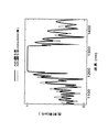
図6には、このようにエッチングされたモニターサンプルにおいてAlAs層が酸化される前後におけるサンプルの反射率の変化が示されている。また、比較のために、図7には、上部DBRをエッチングしなかった場合でのAlAs層が酸化される前後におけるサンプルの反射率の変化が示されている。この時、AlOxの屈折率はおよそ1.76程度として計算した。また、この実施例1では、DBRや共振器は波長1270nmを発振波長として設計されている。
【0049】
図6を図7と比べると分かるように、いずれの場合も、メインローブにおいては反射率はほとんど変化せず、サイドロ−ブにおいて反射率が変化している様子がわかる。DBRをエッチングしないサンプルでの反射率の変化は、AlAs層の厚さが薄いこともあり、その変化は比較的小さく、かつ、反射率が高くなる部分と低くなる部分とが比較的短周期(数十nm周期)に現れているのが分かる。それに対して、AlAs層から1周期上部のGaInP層までエッチングしてある場合は、例えば1050−1150nmや1350−1450nmの範囲で比較するとはっきり分かるが、反射率の変化も大きくなり、また反射率の高くなる部分と低くなる部分の周期も長くなる(100nm以上の周期となる)。
【0050】
反射率を用いてアパーチャ径を制御する方法は以下のようなものである。
【0051】
すなわち、上記のモニターサンプルと同じ構造で作成したサンプルにおいて、この反射率変化の大きい波長域の光(例えばこの実施例1では1350−1450nmの範囲)を用いてモニターサンプル上に照射した光の平均反射率を計測しながらあらかじめ酸化反応を行なう時間をある程度の幅でふって、選択酸化を行なっておく。これにより、酸化を終わったサンプルのアパーチャ径と平均反射率の変化との相関をあらかじめ計測しておくことができる。この時、相関は、例えば図8に示すような関係となる。この関係は、光の照射条件、照射範囲、メサ形状、積層構造が同一であれば、アパーチャ径に対して一意に決まるため、この相関に基づいてあらかじめ希望のアパーチャ径に達した時の平均反射率の値を求めておき、本番の反応においてはその値をもってエンドポイントを確認することで、アパーチャ径を制御して酸化を行なうことが可能になる。
【0052】
あるいは別の方法としては、実際のデバイスよりもわずかにメサの径が小さいモニターサンプルを用意しておき、選択酸化の際に平均反射率を、この実施例1のサンプルにおいては例えば1350−1450nmの範囲の光を用いて計測しつつ、酸化を行ない、平均反射率の値が、あらかじめ求めておいた完全に酸化された時の平均反射率の値と一致したときに酸化反応を止めることで、実デバイスではある一定のアパーチャ径を残して酸化をストップすることができる。当然モニターサンプルのメサ径を調整することで、任意のアパーチャ径に対してエンドポイントを判定するためのモニターサンプルを設定することができる。さらに別の方法としては平均反射率の変化率を用いる方法がある。当然、モニターサンプルがすべて酸化されれば、その時の平均反射率の変化率は0となるので、これをもってモニターサンプルの酸化反応のエンドポイントを知ることもできる。
【0053】
平均反射率の変化率をもって酸化反応のエンドポイントを知る方法は、何も変化率が0となる点を利用するものとは限らない。例えば、この実施例1のように円形のメサ状のモニターサンプルの場合、図8に示すような平均反射率とアパーチャ径との相関を持つわけであるが、この場合、ある程度アパーチャ径が残っていた方が平均反射率の変化率が大きいことが分かる。そのため、モニターサンプルに実デバイスより大きなメサ径を持たせておくことで、エンドポイント見極め時の平均反射率の変化率を大きくすることができる。あらかじめ相関さえ把握しておけば、平均反射率の変化を測定しやすくなる分、制御が行ないやすくなる。
【0054】
このように、実デバイスとモニターサンプルとの間で、酸化反応時に、モニターサンプルの平均反射率と実デバイスのアパーチャ径との相関が一意に決まるようなものであれば、上記のように例えばメサ径や形状が実デバイスとモニターサンプルとである程度異なっていてもかまわない。
【0055】
以上のような方法により酸化の制御を行なう場合には、例えばグレーティングなどを用いて白色光源から反射率の変化が大きくなる部分の波長の光を取り出して反射率を測定することでS/N比を高くすることが考えられるが、上記のように上部DBRの一部をエッチングしたサンプルでは、反射率の変化する部分において、その変化量がエッチングしないサンプルに比べて大きい。また、反射率の増減の周期も長いので、バンドパスフィルタなどにより反射率が増加する(あるいは減少する)波長域の光を取り出してモニターサンプルへ照射し、平均反射率を求めるような場合においても、比較的広い範囲の波長を選択して用いることができるため、より望ましいといえる。
【0056】
また、メサ径が小さいサンプルでメサあたりの反射光が少なくなり計測しにくいような場合には、複数のモニターサンプル用のメサを隣接してある程度の範囲を持って形成し、その範囲での反射率を計測するようにすることで、S/N比を向上させることができる。
【0057】
以上のことから、選択酸化においてアパーチャ径の制御を行なうに際して、上記のような上部DBRの一部をエッチングしたモニターサンプルを設けて上記のような方法によりモニターすることで、選択酸化の制御性を上げることができ、アパーチャ径を絞り、特性の優れた面発光型半導体レーザを歩留まり良く作製することが可能になる。
【0058】
また、GaInPのようにInを含む層をエッチングストップ層として用いることで、反応性イオンエッチングのようなドライエッチングにおいて、比較的制御性良くエッチングストップを行なえるため、あらかじめ反射率の変化を予想できることから、より好ましい波長範囲を予想して、選択酸化制御時の反射率測定を行なうことができ、これにより正確な制御が行なえるようになる。
【0059】
さらに、選択酸化の際の被酸化層としてAlAs層を用いることで、GaAs基板上でのAlGaAs/GaAs系のDBRと被酸化層を同一の結晶成長過程で成長できる。AlGaAs/GaAs系のDBRは、AlGaAsが任意のAl組成においてGaAs基板上で格子整合し、熱伝導も比較的良好で屈折率差も大きく取れるため良好なDBRを得ることができる。実際、0.85μm帯および0.98μm帯の面発光型半導体レーザは、AlGaAs/GaAs積層型のDBRを用いて実際に製造販売されており、GaAs基板上の面発光型半導体レーザにおいては、このAlGaAs/GaAs積層型のDBRは必須ともいえるものである。よって、AlAs酸化層を用いることで良好な制御性で酸化狭窄を行なって、GaAs基板上に面発光型半導体レーザを得ることが可能になる。
【0060】
この実施例1では、1270nmの発振波長を持つ面発光型半導体レーザについて示したが、必ずしもこの波長に限定されるものではなく、より短波の面発光型半導体レーザについても適用される。
【0061】
しかしながら、1200nm以上の長波長においては、DBRの1/4λ低屈折率層としてすべてをAlAs層とするような場合は、層の厚さが100nmを越えてしまう。そのため、信頼性,酸化速度の制御性等の点からは、上記実施例1のようにAlAs層を50nm以下にし、AlGaAs層との積層にして低屈折率層の一部としてしまうことが通常良く行なわれる。すなわち1200nm以上の発振波長を持つ面発光型半導体レーザにおいては、AlAs層の含まれる低屈折率層においてAlAsの占める厚さの割合が必然的に小さくなる。そのような場合でも、本発明を用いることで、1200nm以上の発振波長をもちAlAs層の厚さを50nm以下にしたような場合でも、反射率の変化から制御性良く選択酸化をコントロールできるようになる。
【0062】
実施例2
図9は実施例2の半導体製造装置を示す図である。図9の半導体製造装置では、グレーティングにより白色光源から特定波長の光を光ファイバーに導入して酸化炉内のモニターサンプルへ照射できるようになっており、また、モニターサンプルからの反射光は、光ファイバーで光検出器へと送られるようになっている。この時、光照射の範囲を絞るためのレンズを設けたりしてももちろんかまわない。モニターサンプルは、あらかじめ上部DBRの一部をエッチングしてあり、あらかじめ反射率が酸化によって大きく変化する波長を求めておき、その波長の光をグレーティングにより選択し、光ファイバーを通して酸化炉内のモニターサンプルへ照射できるようになっている。
【0063】
モニターサンプルから反射した光は、光ファイバーを通して光検出器へと導かれる。光検出器としては、例えば測定波長に対して感度を有するフォトディテクタを用いることができる。このフォトディテクタは、例えば増幅器などを介してA/Dコンバータなどに接続され、その値をデジタル変換し、表示器に表示したり、コンピューター上で処理したりすることができるようになっている。当然この測定した値から反射率を求めてコンピュータ上で制御を行なうことも可能である。
【0064】
また、光の照射範囲をコントロールしたり、より効率的に反射光を取りこむために光ファイバーの先端にレンズを組み合わせることも可能である。
【0065】
以上のような構成により、酸化反応を行ないながらモニターサンプルに特定波長の光を照射し、その反射率を測定することが可能になる。
【0066】
図9のような装置で選択酸化を行ない、実施例1で示したような方法を用いれば制御性良く選択酸化を行なうことができる。
【0067】
実施例3
図10は実施例3の半導体製造装置を示す図である。図10の半導体製造装置の基本構成は、実施例2の半導体製造装置と同じであるが、この実施例3では、照射する光の波長を選択する方法として、バンドパスフィルタを用いている。この実施例3では、例えば計算であらかじめ求めておいた、反射率が酸化によって大きく変化する波長域を透過するフィルターを用いてその波長範囲の平均反射率を求めて、選択酸化の際の制御を行なうことができる。この時、例えば酸化によって反射率が高くなるような波長域を透過する複数の種類のバンドパスフィルタ(図6に示したようなサンプルの場合、例えば1350nm−1450nm範囲の複数のフィルタ)を用意しておき、これを短時間で切り替えながら光を照射し、その平均反射率の変化を求めることで、より広い波長範囲での反射率変化を利用することが可能になる。そのため、アパーチャ径と平均反射率との相関をより精度良く求めることが可能になり、より選択酸化を厳密に制御することが可能になる。
【0068】
実施例4
図11は本発明のGaInNAs活性層を有する面発光型半導体レーザ素子の一例を示す図である。図11に示すように、本発明は、酸化狭窄によるアパーチャ径を3μm程度へ絞るようなきわめて制御が難しいような場合においても歩留まりを上げるのに効果を発揮する。このようにシングルモードで発振する面発光型半導体レーザは光通信の分野では非常に望まれるものである。特にGaInNAsを用いた面発光型半導体レーザは、1.2−1.3μm帯での発振を得られる素子であり、これらの波長では石英系の光ファイバに対しての損失が少ないなどの理由により、通信用の光源として好適であるとされている。
【0069】
本発明では、制御性良く選択酸化を行ないアパーチャ径をシングルモード発振に必要な小さい径に絞るような場合でも、面発光型半導体レーザ素子の特性を制御性良く安定に作ることができる。
【0070】
また、GaInNAs活性層を用いることで、石英系の光ファイバに対しての損失が少ない面発光型半導体レーザをより安定な特性で得ることが可能になる。
【0071】
実施例5
図12は本発明の光送受信モジュールの一例を示す図である。図12の光送受信モジュールは、実施例4の面発光型半導体レーザ素子と受信用フォトダイオードと光ファイバーとを組み合わせたものとなっている。
【0072】
本発明による面発光型半導体レーザ素子を光通信システムに用いる場合、面発光型半導体レーザ素子は低コストであるので、図12に示すように送信用の面発光型半導体レーザ素子(例えば1.3μm帯GaInNAs面発光型半導体レーザ素子)と、受信用フォトダイオードと、光ファイバーとを組み合わせた光送信モジュールを低コストで得られる。
【0073】
GaInNAsを用いた面発光型半導体レーザは、1.2−1.3μm帯での発振を得られる素子として知られており、これらの波長では石英系の光ファイバに対しての損失が少ないなどの理由により、通信用の光源として有望視されている。さらには、特に1.3μm等の長波長帯で低損失となるフッ素添加POF(プラスチックファイバ)とGaInNAsを活性層に用いた面発光型レーザとを組み合わせるとファイバが低コストであること、ファイバの径が大きくてファイバとのカップリングが容易で実装コストを低減できることから、極めて低コストのモジュールを実現できる。また、GaInNAsはその優れた温度特性から、強力な冷却用の構成を必要としない。そのため、冷却用のコストが削減でき、小型で安価な光通信モジュールを得られる。
【0074】
本発明によれば、AlAs層を制御良く選択酸化することで、シングルモード発振に必要な酸化狭窄径を有する面発光型半導体レーザを歩留まり良く得ることができるため、光通信に好適な面発光型半導体レーザ素子を製造することがより容易に行なえるようになり、高性能の通信用長波長帯面発光型半導体レーザ素子を実現でき、さらにこれらの素子を用いると、低コストの光ファイバー通信システム,光インターコネクションシステムなどの光通信システムを実現することができる。
【0075】
【発明の効果】
以上に説明したように、請求項1記載の発明によれば、酸化炉内において、半導体多層膜構造に被酸化層を含む被測定物に光を照射し、酸化反応中の被測定物からの反射光を検出し、前記反射光の反射率、平均反射率、反射率の変化率、平均反射率の変化率を演算し、該演算結果に基づき酸化反応の進行を検出し、酸化反応の制御を行なう半導体製造方法において、前記被測定物は、半導体基板上のモニターサンプルであり、かつ半導体多層膜構造の被酸化層よりも上部の少なくとも一部がエッチングにより除去されていることで、被酸化層の酸化によるモニターサンプルの反射率の変化を大きくし、酸化反応の制御性を向上させることができる。
【0076】
また、請求項2記載の発明によれば、請求項1記載の半導体製造方法において、半導体多層膜中の被酸化層よりも上部にエッチングストップ層を設け、モニターサンプルにおいてはエッチングストップ層によりエッチング深さを一定とすることで、反射率の変化をあらかじめ予想し計測できるようになり、一定の条件で制御ができ、酸化反応の制御性を向上させることができる。
【0077】
また、請求項3記載の発明によれば、酸化炉内において、半導体多層膜構造に被酸化層を含む被測定物に光を照射し、酸化反応中の被測定物からの反射光を検出し、前記反射光の反射率、平均反射率、反射率の変化率、平均反射率の変化率を演算し、該演算結果に基づき酸化反応の進行を検出し、酸化反応の制御を行なう面発光型半導体レーザの製造方法において、被酸化層として電流狭窄構造を選択酸化によって形成するためのAlAs層を設けたことで、GaAs基板上にAlGaAs/GaAs系DBRを採用した面発光型半導体レーザの製造において酸化反応の制御性を向上できるようになる。
【0078】
また、請求項4記載の発明によれば、請求項3記載の面発光型半導体レーザの製造方法において、半導体多層膜構造にAlGaAs/GaAsの積層による分布ブラッグ反射鏡を含み、被酸化層であるAlAs層よりも上部にエッチングストップ層としてGaInP,GaInP,AlInP,GaInAsP,AlInAsP,AlGaInP,AlGaInAsP層のいずれかを設けたことで、反応性イオンエッチング等のドライエッチングにおいて、制御性良くエッチングストップを行なえるようになり、その結果、反射率の変化をあらかじめ予想し計測できるようになり、一定の条件で制御ができ、酸化反応の制御性を向上させることができる。
【0079】
また、請求項5記載の発明によれば、請求項3または請求項4記載の面発光型半導体レーザの製造方法において、発振波長が1200nm以上であり、かつ、AlAs層の厚さが50nm以下である場合においても、より制御性の高い酸化の制御を有効に行なって選択酸化を行ない、面発光型半導体レーザを製造できる。
【0080】
また、請求項6記載の発明によれば、請求項3乃至請求項5のいずれか一項に記載の面発光型半導体レーザの製造方法により作製された面発光型半導体レーザ素子であるので、より酸化の制御性を向上し、歩留まり良く、特性の安定した面発光型半導体レーザ素子を提供することができる。
【0081】
また、請求項7記載の発明によれば、請求項6記載の面発光型半導体レーザ素子において、活性層がGaInNAsであることにより、選択酸化の制御性を良くすることができ、歩留まり良く特性のそろった1.2−1.3μm帯での発振が得られる面発光型半導体レーザ素子を提供することができる。
【0082】
また、請求項8記載の発明によれば、請求項7記載の面発光型半導体レーザ素子を用いたことで(すなわち、歩留まり良く、特性のそろった1.2−1.3μm帯での発振を得られる面発光型半導体レーザ素子を用いたことで)、低コストで特性の優れた小型の光送信モジュールを提供することができる。
【0083】
また、請求項9記載の発明によれば、請求項7記載の面発光型半導体レーザ素子を用いたことで(すなわち、歩留まり良く、特性のそろった1.2−1.3μm帯での発振を得られる面発光型半導体レーザ素子を用いたことで)、低コストで特性の優れた小型の光送受信モジュールを提供することができる。
【0084】
また、請求項10記載の発明によれば、請求項7記載の面発光型半導体レーザ素子を用いたことで(すなわち、歩留まり良く、特性のそろった1.2−1.3μm帯での発振を得られる面発光型半導体レーザ素子を用いたことで)、低コストで小型の光通信システムを提供できる。
【図面の簡単な説明】
【図1】AlAsの層厚を例えば50nm以下程度の比較的薄い厚さにし、AlAsを面発光型半導体レーザのDBRにおける低屈折率層の一部として例えばAlGaAs層に挟まれた形で用いる構成を示す図である。
【図2】図1の構成において、低屈折率層の一部であるAlAs層の酸化によるVCSEL構造全体の反射率の変化を示す図である。
【図3】本発明の半導体製造方法によって作製された半導体分布ブラッグ反射鏡を含む面発光型半導体レーザの一例を示す図である。
【図4】AlAs層を含む低屈折率層を示す図である。
【図5】モニター用サンプルを示す図である。
【図6】モニターサンプルにおいてAlAs層が酸化される前後におけるサンプルの反射率の変化を示す図である。
【図7】上部DBRをエッチングしなかった場合でのAlAs層が酸化される前後におけるサンプルの反射率の変化を示す図である。
【図8】平均反射率とアパーチャ径との相関を示すである。
【図9】実施例2の半導体製造装置を示す図である。
【図10】実施例2の半導体製造装置を示す図である。
【図11】本発明のGaInNAs活性層を有する面発光型半導体レーザ素子の一例を示す図である。
【図12】本発明の光送受信モジュールの一例を示す図である。[0001]
TECHNICAL FIELD OF THE INVENTION
The present invention relates to a semiconductor manufacturing method, a surface-emitting type semiconductor laser manufacturing method, a surface-emitting type semiconductor laser device, an optical transmission module, an optical transmission / reception module, and an optical communication system.
[0002]
[Prior art]
A surface emitting semiconductor laser (VCSEL: Vertical Cavity Surface Emitting Laser) has many advantages over an edge emitting semiconductor laser, such as low manufacturing cost and easy integration in an array. It is expected to be used in many fields such as optical communication, optical interconnection, and optical recording.
[0003]
Among the surface-emitting type semiconductor lasers, a selective oxidation type VCSEL is one of the most promising from the viewpoint of laser characteristics such as a threshold current value and power consumption. This means that during crystal growth, an AlAs layer (or an AlGaAs layer having an Al composition very close to 1) is grown as a part of a distributed Bragg reflector (DBR: Distributed Bragg Reflector), and this AlAs layer is selectively oxidized. The current confinement structure is formed in the VCSEL structure. In a selective oxidation type VCSEL, a current confinement structure is manufactured by using a selective oxidation process of AlAs or AlGaAs after crystal growth. Don't worry.
[0004]
For example, in the case where the diameter of the opening (aperture) of AlAs remaining without being oxidized is about several μm, when a current is injected into the surface-emitting type semiconductor laser through the electrodes on both sides, the injected current is reduced to the non-oxidized mesa. The selective oxidation type VCSEL has excellent laser characteristics, such as being confined to only a few μm at the center of the shape and exhibiting a low threshold current value.
[0005]
At this time, laser characteristics such as a threshold current value largely depend on the diameter of the aperture. The most frequently used selective oxidation method is a wet oxidation method. This is a method of bubbling pure water heated to 80 to 100 ° C. using nitrogen as a carrier gas, transporting the steam to a furnace, and selectively oxidizing only a part of the AlAs or AlGaAs layer. The temperature of the oxidation furnace is usually from 400 to 500 ° C. Conventionally, oxidation experiments by this oxidation process are repeatedly performed under various conditions using an oxidation furnace actually used, and oxidation is performed under optimized conditions based on the obtained results to produce a selective oxidation type VCSEL. Was.
[0006]
As a method for stably performing the selective oxidation process with good reproducibility, there is a method described in JP-A-2001-93897. In this method, a light source for irradiating light and a means for detecting reflected light are provided in an oxidation furnace, and the refractive index of a layer to be oxidized (for example, AlAs) is changed due to an oxidation reaction. Utilizing the fact that the rate changes, the degree of progress of the oxidation reaction is determined and controlled.
[0007]
[Problems to be solved by the invention]
However, the above-described conventional method for performing the selective oxidation process with good reproducibility and stability has the following problems. That is, the AlAs layer changes to AlOx by being oxidized, but at this time, the volume expands. This volume expansion is naturally larger as the thickness of the layer is larger. However, if the volume expansion is too large, defects are likely to be introduced into the crystal, which is not preferable in terms of reliability. For this reason, it is generally considered undesirable to make the AlAs layer too thick. In addition, since the oxidation rate generally increases as the layer thickness increases, especially when it is desired to reduce the diameter of the aperture due to oxidation constriction, the layer thickness is reduced to some extent to suppress the oxidation rate in order to improve controllability. Have been.
[0008]
In the case where the thickness of the AlAs layer is not desired to be too large as described above, particularly when the oscillation wavelength is longer than 1200 nm, the thickness of each low refractive index layer becomes large, and it is not preferable that all of the layers are AlAs layers. Is to make the layer thickness of AlAs relatively thin, for example, about 50 nm or less, and to use AlAs as a part of a low refractive index layer in a DBR of a surface emitting semiconductor laser, for example, sandwiched between AlGaAs layers ( See FIG. 1). In this case, the change in the reflectance of the entire VCSEL structure due to oxidation of the AlAs layer which is a part of the low refractive index layer becomes smaller as the thickness of the AlAs is reduced (see FIG. 2). As described above, when the thickness of the AlAs layer is small, there is a problem that it is difficult to determine an end point for performing control as the change in reflectance becomes small.
[0009]
The present invention relates to a method for manufacturing a semiconductor, a method for manufacturing a surface-emitting type semiconductor laser, and a method for manufacturing a surface-emitting type semiconductor laser capable of favorably controlling oxidation narrowing based on a change in reflectance even when the thickness of the AlAs layer is relatively small. It is an object of the present invention to provide a semiconductor laser device, an optical transmitting module, an optical transmitting / receiving module, and an optical communication system.
[0010]
[Means for Solving the Problems]
In order to achieve the above object, the invention according to claim 1 irradiates light to an object to be measured including a layer to be oxidized in a semiconductor multilayer film structure in an oxidation furnace, and reflects the light from the object during the oxidation reaction. Detect the light, calculate the reflectance of the reflected light, the average reflectance, the change rate of the reflectance, the change rate of the average reflectance, detect the progress of the oxidation reaction based on the calculation result, and control the oxidation reaction. In the semiconductor manufacturing method to be performed, the object to be measured is a monitor sample on a semiconductor substrate, and at least a part of an upper part of the oxidized layer of the semiconductor multilayer structure is removed by etching. I have.
[0011]
According to a second aspect of the present invention, in the method of manufacturing a semiconductor according to the first aspect, an etching stop layer is provided above the layer to be oxidized in the semiconductor multilayer film. It is characterized by being constant.
[0012]
Further, the invention according to claim 3 is characterized in that, in an oxidation furnace, the object to be measured including the layer to be oxidized in the semiconductor multilayer film structure is irradiated with light, and reflected light from the object to be measured during the oxidation reaction is detected. A surface-emitting type semiconductor laser that calculates the reflectance of reflected light, the average reflectance, the rate of change of the reflectance, and the rate of change of the average reflectance, detects the progress of the oxidation reaction based on the calculation result, and controls the oxidation reaction. Is characterized in that an AlAs layer for forming a current confinement structure by selective oxidation is provided as a layer to be oxidized.
[0013]
According to a fourth aspect of the present invention, in the method of manufacturing a surface emitting semiconductor laser according to the third aspect, the semiconductor multilayer film structure includes a distributed Bragg reflector formed by stacking AlGaAs / GaAs, and the AlAs layer serving as an oxidized layer. Any one of GaInP, GaInP, AlInP, GaInAsP, AlInAsP, AlGaInP, and AlGaInAsP layers is provided as an etching stop layer above.
[0014]
According to a fifth aspect of the present invention, in the method of manufacturing a surface emitting semiconductor laser according to the third or fourth aspect, the oscillation wavelength is 1200 nm or more and the thickness of the AlAs layer is 50 nm or less. Features.
[0015]
According to a sixth aspect of the present invention, there is provided a method of manufacturing a surface emitting semiconductor laser according to any one of the third to fifth aspects.
[0016]
According to a seventh aspect of the present invention, in the surface emitting semiconductor laser device according to the sixth aspect, the active layer is made of GaInNAs.
[0017]
An eighth aspect of the present invention is an optical transmission module using the surface emitting semiconductor laser device according to the seventh aspect.
[0018]
According to a ninth aspect of the present invention, there is provided an optical transceiver module using the surface emitting semiconductor laser device according to the seventh aspect.
[0019]
According to a tenth aspect of the present invention, there is provided an optical communication system using the surface emitting semiconductor laser device according to the seventh aspect.
[0020]
BEST MODE FOR CARRYING OUT THE INVENTION
Hereinafter, embodiments of the present invention will be described with reference to the drawings.
[0021]
First embodiment
In the semiconductor manufacturing method according to the first embodiment of the present invention, an object to be measured including a layer to be oxidized in a semiconductor multilayer film structure is irradiated with light in an oxidation furnace, and reflected light from the object to be measured during an oxidation reaction is emitted. A semiconductor for detecting and calculating the reflectance of the reflected light, the average reflectance, the rate of change of the reflectance, and the rate of change of the average reflectance, detecting the progress of the oxidation reaction based on the calculation result, and controlling the oxidation reaction In the manufacturing method, the object to be measured is a monitor sample on a semiconductor substrate, and at least a part of the semiconductor multilayer structure above the layer to be oxidized is removed by etching.
[0022]
As described above, in the first embodiment of the present invention, in the oxidation furnace, the object to be measured including the layer to be oxidized in the semiconductor multilayer film structure is irradiated with light, and the reflected light from the object to be measured during the oxidation reaction is emitted. A semiconductor for detecting and calculating the reflectance of the reflected light, the average reflectance, the rate of change of the reflectance, and the rate of change of the average reflectance, detecting the progress of the oxidation reaction based on the calculation result, and controlling the oxidation reaction In the manufacturing method, the object to be measured is a monitor sample on a semiconductor substrate, and at least a part of the semiconductor multilayer structure above the layer to be oxidized is removed by etching, thereby oxidizing the layer to be oxidized. , The change in the reflectance of the monitor sample caused by the reaction can be increased, and the controllability of the oxidation reaction can be improved.
[0023]
Further, in the semiconductor manufacturing method of the first embodiment, an etching stop layer is provided above the layer to be oxidized in the semiconductor multilayer film, and in the monitor sample, the etching depth can be made constant by the etching stop layer. .
[0024]
Thus, by providing the etching stop layer above the layer to be oxidized in the semiconductor multilayer film and making the etching depth constant by the etching stop layer in the monitor sample, it is possible to predict and measure the change in reflectance in advance. As a result, control can be performed under certain conditions, and controllability of the oxidation reaction can be improved.
[0025]
Second embodiment
The method for manufacturing a surface-emitting type semiconductor laser according to the second embodiment of the present invention includes the steps of: irradiating an object to be measured including a layer to be oxidized in a semiconductor multilayer film structure with light in an oxidation furnace; From the reflected light, calculate the reflectance of the reflected light, the average reflectance, the rate of change of the reflectance, the rate of change of the average reflectance, based on the calculation result, detect the progress of the oxidation reaction, In the method for manufacturing a surface-emitting type semiconductor laser which performs the above control, an AlAs layer for forming a current confinement structure by selective oxidation is provided as a layer to be oxidized.
[0026]
As described above, in the second embodiment of the present invention, the object to be measured including the layer to be oxidized in the semiconductor multilayer structure is irradiated with light in the oxidation furnace, and the reflected light from the object to be measured during the oxidation reaction is emitted. Detecting, calculating the reflectance of the reflected light, the average reflectance, the change rate of the reflectance, the change rate of the average reflectance, detecting the progress of the oxidation reaction based on the calculation result, and controlling the oxidation reaction. In the method of manufacturing a light emitting semiconductor laser, an AlAs layer for forming a current confinement structure by selective oxidation is provided as a layer to be oxidized, so that a surface emitting semiconductor laser employing an AlGaAs / GaAs DBR on a GaAs substrate. It becomes possible to improve the controllability of the oxidation reaction in the production.
[0027]
In the method for manufacturing a surface emitting semiconductor laser according to the second embodiment, the semiconductor multilayer film structure includes a distributed Bragg reflector formed by stacking AlGaAs / GaAs, and serves as an etching stop layer above the AlAs layer to be oxidized. Any one of GaInP, GaInP, AlInP, GaInAsP, AlInAsP, AlGaInP, and AlGaInAsP layers can be provided.
[0028]
As described above, in the method for manufacturing the surface emitting semiconductor laser according to the second embodiment, the semiconductor multilayer film structure includes the distributed Bragg reflector formed by stacking AlGaAs / GaAs, and is etched above the AlAs layer that is the layer to be oxidized. By providing any one of the GaInP, GaInP, AlInP, GaInAsP, AlInAsP, AlGaInP, and AlGaInAsP layers as the stop layer, it becomes possible to perform an etching stop with good controllability in dry etching such as reactive ion etching. In addition, a change in reflectance can be predicted and measured in advance, control can be performed under certain conditions, and controllability of the oxidation reaction can be improved.
[0029]
Further, in the second embodiment, even when the oscillation wavelength of the surface-emitting type semiconductor laser is 1200 nm or more and the thickness of the AlAs layer is 50 nm or less, it is possible to effectively control the oxidation with higher controllability. Then, selective oxidation is performed to manufacture a surface emitting semiconductor laser.
[0030]
Third embodiment
The third embodiment of the present invention is a surface-emitting type semiconductor laser device manufactured by the method for manufacturing a surface-emitting type semiconductor laser of the second embodiment.
[0031]
Since the surface-emitting type semiconductor laser device of the third embodiment is a surface-emitting type semiconductor laser device manufactured by the method of manufacturing the surface-emitting type semiconductor laser of the second embodiment, the controllability of oxidation is further improved. As a result, it is possible to provide a surface-emitting type semiconductor laser device with good yield and stable characteristics.
[0032]
In the surface emitting semiconductor laser device according to the third embodiment, the active layer can be made of GaInNAs.
[0033]
As described above, in the surface-emitting type semiconductor laser device of the third embodiment, when the active layer is made of GaInNAs, the controllability of selective oxidation can be improved, and the characteristics can be improved with a good yield. It is possible to provide a surface-emitting type semiconductor laser device which can oscillate in a 1.3 μm band.
[0034]
Fourth embodiment
The fourth embodiment of the present invention is an optical transmission module using the surface emitting semiconductor laser device of the third embodiment.
[0035]
In the fourth embodiment, by using the surface-emitting type semiconductor laser device of the third embodiment (that is, a surface capable of obtaining an oscillation in the 1.2-1.3 μm band with good yield and uniform characteristics). By using the light emitting semiconductor laser device), it is possible to provide a small-sized optical transmission module having excellent characteristics at low cost.
[0036]
Fifth embodiment
The fifth embodiment of the present invention is an optical transceiver module using the surface emitting semiconductor laser device of the third embodiment.
[0037]
In the fifth embodiment, the surface-emitting type semiconductor laser device of the third embodiment is used (that is, a surface which can obtain oscillation in the 1.2-1.3 μm band with good yield and uniform characteristics). By using the light emitting semiconductor laser device), it is possible to provide a small-sized optical transceiver module having excellent characteristics at low cost.
[0038]
Sixth embodiment
The sixth embodiment of the present invention is an optical communication system using the surface emitting semiconductor laser device of the third embodiment.
[0039]
In the sixth embodiment, by using the surface emitting semiconductor laser device of the third embodiment (that is, a surface capable of obtaining oscillation in the 1.2-1.3 μm band with good yield and uniform characteristics). By using the light emitting semiconductor laser device), it is possible to provide a low-cost and compact optical communication system.
[0040]
【Example】
Hereinafter, examples of the present invention will be described.
[0041]
Example 1
FIG. 3 is a diagram showing an example of a surface emitting semiconductor laser including a semiconductor distributed Bragg reflector manufactured by the semiconductor manufacturing method of the present invention.
[0042]
In the surface-emitting type semiconductor laser of FIG. 3, a low refractive index including an n-type semiconductor multilayer mirror, a GaAs lower spacer layer, a GaInNAs / GaAs multiple quantum well active layer, a GaAs upper spacer layer, and an AlAs layer on an n-type GaAs substrate. An index layer and a p-type semiconductor multilayer film reflecting mirror are sequentially formed.
[0043]
Here, as shown in FIG. 4, the low refractive index layer including the AlAs layer is formed so that the entire optical length is 3 / 4λ. The thickness of the low refractive index layer may be an odd multiple of 4λ, and does not necessarily have to be / λ. This low refractive index layer is made of Al0.9Ga0.1It is composed of an As layer and an AlAs layer, and the AlAs layer has a thickness of, for example, 30 nm.
[0044]
In the surface-emitting type semiconductor laser of FIG. 3, a GaAs high refractive index layer having a thickness of λλ is provided above the low refractive index layer including the AlAs layer, and, for example, a GaInP low refractive index layer is provided thereon. Are provided with a thickness of 1 / λ.
[0045]
The steps for fabricating this surface emitting semiconductor laser are as follows.
[0046]
That is, first, GaAs and Al are deposited on an n-type GaAs substrate by metal organic chemical vapor deposition (MOCVD).0.9Ga0.1As is alternately stacked (for example, 35 periods) with a thickness such that the optical length becomes 4λ with respect to the oscillation wavelength of the laser to form a lower DBR (n-type semiconductor multilayer film reflecting mirror). A resonator structure having an optical length of λ in which a quantum well active layer composed of a GaInNAs layer is sandwiched between GaAs spacer layers is formed, and an upper DBR (p-type semiconductor multilayer film reflection) starting from a low refractive index layer including an AlAs layer is further formed thereon. (Mirror) (for example, 25 periods).
[0047]
Next, the above laminated structure is etched to below the active layer by reactive ion etching, and is processed into a post-shaped mesa of, for example, about 50 μmφ. At this time, for example, a mesa for monitoring is formed near the device in the same shape. Next, a part of the upper DBR is etched only for the mesa for monitoring using the same reactive ion etching. At this time, since the GaInP low refractive index layer contains In, the etching rate is greatly reduced during dry etching. Therefore, it is easy to stop the reactive ion etching in the GaInP layer by using it together with time management. As a result, the monitor sample is etched up to the GaInP layer one cycle higher than the low refractive index layer including the AlAs layer (see FIG. 5).
[0048]
FIG. 6 shows a change in reflectance of the monitor sample thus etched before and after the AlAs layer is oxidized. For comparison, FIG. 7 shows a change in the reflectance of the sample before and after the AlAs layer was oxidized when the upper DBR was not etched. At this time, the calculation was performed on the assumption that the refractive index of AlOx was about 1.76. In the first embodiment, the DBR and the resonator are designed with the wavelength of 1270 nm as the oscillation wavelength.
[0049]
As can be seen from a comparison between FIG. 6 and FIG. 7, in any case, the reflectance is hardly changed in the main lobe, and the reflectance is changed in the side lobe. The change in the reflectance of the sample in which the DBR is not etched may be relatively small because the thickness of the AlAs layer may be small, and the portion where the reflectance is high and the portion where the reflectance is low may have a relatively short period ( It can be seen that it appears in a period of several tens of nm. On the other hand, when the etching is performed from the AlAs layer to the GaInP layer one cycle above, for example, when the comparison is made in the range of 1050 to 1150 nm or 1350 to 1450 nm, the change in the reflectivity becomes large, and the change in the reflectivity becomes large. The period of the higher portion and the lower portion also becomes longer (has a period of 100 nm or more).
[0050]
The method of controlling the aperture diameter using the reflectance is as follows.
[0051]
That is, in a sample prepared with the same structure as the above-mentioned monitor sample, the average of the light irradiated on the monitor sample using the light in the wavelength range where the reflectance change is large (for example, in the range of 1350-1450 nm in Example 1). While measuring the reflectance, the time for performing the oxidation reaction is varied in a certain range in advance to perform the selective oxidation. This makes it possible to measure in advance the correlation between the aperture diameter of the oxidized sample and the change in the average reflectance. At this time, the correlation is, for example, as shown in FIG. This relationship is uniquely determined with respect to the aperture diameter if the light irradiation condition, irradiation range, mesa shape, and lamination structure are the same, and based on this correlation, the average reflection when the desired aperture diameter is reached in advance is determined. By determining the value of the rate and confirming the end point with the value in the actual reaction, the oxidation can be performed by controlling the aperture diameter.
[0052]
Alternatively, as another method, a monitor sample having a mesa diameter slightly smaller than that of an actual device is prepared, and the average reflectance at the time of selective oxidation is set to, for example, 1350-1450 nm in the sample of Example 1. By oxidizing while measuring using light in the range, by stopping the oxidation reaction when the value of the average reflectance matches the value of the average reflectance when completely oxidized previously determined, In an actual device, oxidation can be stopped while leaving a certain aperture diameter. Of course, by adjusting the mesa diameter of the monitor sample, it is possible to set the monitor sample for determining the end point for an arbitrary aperture diameter. As still another method, there is a method using a change rate of the average reflectance. Naturally, if all the monitor samples are oxidized, the change rate of the average reflectance at that time becomes 0, so that the end point of the oxidation reaction of the monitor sample can be known from this.
[0053]
The method of knowing the end point of the oxidation reaction based on the change rate of the average reflectance does not always use the point where the change rate becomes zero. For example, in the case of a circular mesa-shaped monitor sample as in the first embodiment, there is a correlation between the average reflectance and the aperture diameter as shown in FIG. 8, but in this case, the aperture diameter remains to some extent. It can be seen that the change rate of the average reflectance is larger when the value is larger. Therefore, by giving the monitor sample a mesa diameter larger than that of the actual device, the rate of change of the average reflectance when determining the end point can be increased. If the correlation is grasped in advance, the change in the average reflectance becomes easier to measure, so that the control becomes easier.
[0054]
Thus, if the correlation between the average reflectance of the monitor sample and the aperture diameter of the actual device is uniquely determined during the oxidation reaction between the actual device and the monitor sample, for example, The diameter and shape may differ to some extent between the actual device and the monitor sample.
[0055]
When the oxidation is controlled by the method described above, the S / N ratio is measured by extracting light having a wavelength where the change in reflectance is large from a white light source using a grating or the like and measuring the reflectance. However, in the sample in which a part of the upper DBR is etched as described above, the amount of change in the portion where the reflectance changes is larger than that in the sample where no etching is performed. In addition, since the period of increase and decrease of the reflectance is long, light in a wavelength region where the reflectance increases (or decreases) by a band-pass filter or the like is taken out and irradiated on a monitor sample to obtain an average reflectance. This can be said to be more desirable because a relatively wide range of wavelengths can be selected and used.
[0056]
Also, if the reflected light per mesa is small and it is difficult to measure a sample with a small mesa diameter, a mesa for multiple monitor samples should be formed with a certain range adjacent to the mesa, and the reflection in that range By measuring the rate, the S / N ratio can be improved.
[0057]
From the above, when the aperture diameter is controlled in the selective oxidation, the controllability of the selective oxidation is improved by providing a monitor sample in which a part of the upper DBR is etched as described above and monitoring by the above method. As a result, the aperture diameter can be reduced, and a surface emitting semiconductor laser having excellent characteristics can be manufactured with high yield.
[0058]
In addition, by using a layer containing In such as GaInP as an etching stop layer, in dry etching such as reactive ion etching, etching can be stopped with relatively controllability, so that a change in reflectance can be predicted in advance. Therefore, the reflectance can be measured during the selective oxidation control in anticipation of a more preferable wavelength range, whereby accurate control can be performed.
[0059]
Further, by using the AlAs layer as the oxidized layer in the selective oxidation, the AlGaAs / GaAs DBR and the oxidized layer on the GaAs substrate can be grown in the same crystal growth process. In the AlGaAs / GaAs DBR, AlGaAs is lattice-matched on a GaAs substrate in an arbitrary Al composition, has relatively good heat conduction, and can obtain a large difference in refractive index, so that a good DBR can be obtained. In fact, surface emitting semiconductor lasers in the 0.85 μm band and 0.98 μm band are actually manufactured and sold using an AlGaAs / GaAs stacked DBR, and in a surface emitting semiconductor laser on a GaAs substrate, An AlGaAs / GaAs stacked DBR is essential. Therefore, by using an AlAs oxide layer, oxidation constriction can be performed with good controllability, and a surface-emitting type semiconductor laser can be obtained on a GaAs substrate.
[0060]
In the first embodiment, a surface-emitting type semiconductor laser having an oscillation wavelength of 1270 nm has been described. However, the present invention is not limited to this wavelength, and the present invention is also applicable to a short-wavelength surface-emitting type semiconductor laser.
[0061]
However, at a long wavelength of 1200 nm or more, when the AlAs layer is used as the Rλ low refractive index layer of the DBR, the thickness of the layer exceeds 100 nm. Therefore, from the viewpoints of reliability, controllability of the oxidation rate, and the like, it is usually good that the AlAs layer is made 50 nm or less as in the first embodiment, and is laminated with the AlGaAs layer to be a part of the low refractive index layer. Done. That is, in a surface emitting semiconductor laser having an oscillation wavelength of 1200 nm or more, the ratio of the thickness occupied by AlAs in the low refractive index layer including the AlAs layer is necessarily small. Even in such a case, by using the present invention, even when the AlAs layer has an oscillation wavelength of 1200 nm or more and the thickness of the AlAs layer is 50 nm or less, the selective oxidation can be controlled with good controllability from the change in the reflectance. Become.
[0062]
Example 2
FIG. 9 is a diagram illustrating a semiconductor manufacturing apparatus according to the second embodiment. In the semiconductor manufacturing apparatus of FIG. 9, light of a specific wavelength is introduced from a white light source into an optical fiber by a grating and can be irradiated on a monitor sample in an oxidation furnace, and reflected light from the monitor sample is transmitted through an optical fiber. It is sent to a photodetector. At this time, of course, a lens for narrowing the range of light irradiation may be provided. For the monitor sample, a part of the upper DBR has been etched in advance, and a wavelength at which the reflectance greatly changes due to oxidation is determined in advance. The light of that wavelength is selected by a grating, and the monitor sample in the oxidation furnace is passed through an optical fiber. Irradiation is possible.
[0063]
Light reflected from the monitor sample is guided through an optical fiber to a photodetector. As the photodetector, for example, a photodetector having sensitivity to a measurement wavelength can be used. The photodetector is connected to an A / D converter or the like via, for example, an amplifier or the like, so that the value can be converted into a digital value, displayed on a display device, or processed on a computer. Naturally, it is also possible to determine the reflectance from the measured value and control the same on a computer.
[0064]
It is also possible to combine a lens with the tip of the optical fiber in order to control the irradiation range of the light or to capture the reflected light more efficiently.
[0065]
With the above configuration, it is possible to irradiate the monitor sample with light of a specific wavelength while performing an oxidation reaction, and to measure the reflectance.
[0066]
When selective oxidation is performed by the apparatus as shown in FIG. 9 and the method described in the first embodiment is used, selective oxidation can be performed with good controllability.
[0067]
Example 3
FIG. 10 is a diagram illustrating a semiconductor manufacturing apparatus according to a third embodiment. The basic configuration of the semiconductor manufacturing apparatus of FIG. 10 is the same as that of the semiconductor manufacturing apparatus of the second embodiment. However, in the third embodiment, a band-pass filter is used as a method for selecting the wavelength of light to be applied. In the third embodiment, for example, the average reflectance in the wavelength range is determined using a filter that transmits the wavelength range in which the reflectance greatly changes due to oxidation, which is determined in advance by calculation, and the control at the time of selective oxidation is performed. Can do it. At this time, for example, a plurality of types of band-pass filters (for example, a plurality of filters in a range of 1350 nm to 1450 nm in the case of the sample shown in FIG. 6) that transmit a wavelength range in which the reflectance increases due to oxidation are prepared. In advance, by irradiating light while switching the light in a short time and calculating a change in the average reflectance, it is possible to use a change in the reflectance in a wider wavelength range. Therefore, the correlation between the aperture diameter and the average reflectance can be obtained with higher accuracy, and the selective oxidation can be more strictly controlled.
[0068]
Example 4
FIG. 11 is a view showing an example of a surface emitting semiconductor laser device having a GaInNAs active layer according to the present invention. As shown in FIG. 11, the present invention is effective in increasing the yield even in the case where it is extremely difficult to control the aperture diameter to about 3 μm due to the oxidized constriction. Such a surface-emitting type semiconductor laser oscillating in a single mode is very desirable in the field of optical communication. In particular, a surface emitting semiconductor laser using GaInNAs is an element capable of obtaining oscillation in the 1.2-1.3 μm band. At these wavelengths, the loss to a quartz-based optical fiber is small. It is said to be suitable as a light source for communication.
[0069]
According to the present invention, even when the aperture diameter is reduced to a small diameter required for single mode oscillation by performing selective oxidation with good controllability, the characteristics of the surface emitting semiconductor laser element can be stably manufactured with good controllability.
[0070]
In addition, by using the GaInNAs active layer, it becomes possible to obtain a surface emitting semiconductor laser with less loss to a quartz optical fiber with more stable characteristics.
[0071]
Example 5
FIG. 12 is a diagram showing an example of the optical transceiver module of the present invention. The optical transceiver module of FIG. 12 is a combination of the surface emitting semiconductor laser device of the fourth embodiment, a receiving photodiode, and an optical fiber.
[0072]
When the surface emitting semiconductor laser device according to the present invention is used in an optical communication system, the surface emitting semiconductor laser device is inexpensive. Therefore, as shown in FIG. 12, a surface emitting semiconductor laser device for transmission (for example, 1.3 μm) is used. An optical transmission module combining a band GaInNAs surface emitting semiconductor laser device), a receiving photodiode, and an optical fiber can be obtained at low cost.
[0073]
A surface emitting semiconductor laser using GaInNAs is known as an element capable of obtaining oscillation in the 1.2-1.3 μm band. At these wavelengths, loss to a quartz-based optical fiber is small. For a reason, it is regarded as a promising light source for communication. Furthermore, the combination of a fluorine-doped POF (plastic fiber), which has a low loss in a long wavelength band such as 1.3 μm, and a surface emitting laser using GaInNAs as an active layer makes the fiber low-cost. Since the diameter is large and coupling with the fiber is easy and the mounting cost can be reduced, an extremely low-cost module can be realized. GaInNAs does not require a powerful cooling structure due to its excellent temperature characteristics. Therefore, the cost for cooling can be reduced, and a small and inexpensive optical communication module can be obtained.
[0074]
According to the present invention, by selectively oxidizing the AlAs layer with good control, a surface-emitting type semiconductor laser having an oxidation confinement diameter required for single mode oscillation can be obtained with a high yield. Semiconductor laser devices can be manufactured more easily, and high-performance long-wavelength surface-emitting semiconductor laser devices for communication can be realized. Further, using these devices, low-cost optical fiber communication systems, An optical communication system such as an optical interconnection system can be realized.
[0075]
【The invention's effect】
As described above, according to the first aspect of the present invention, in an oxidation furnace, an object to be measured including a layer to be oxidized in a semiconductor multilayer film structure is irradiated with light, and the light from the object to be measured during the oxidation reaction is reduced. Detecting the reflected light, calculating the reflectance of the reflected light, the average reflectance, the rate of change of the reflectance, the rate of change of the average reflectance, detecting the progress of the oxidation reaction based on the calculation result, and controlling the oxidation reaction. The object to be measured is a monitor sample on a semiconductor substrate, and at least a part of the upper part of the oxidized layer of the semiconductor multilayer structure is removed by etching, so that The change in the reflectance of the monitor sample due to the oxidation of the layer can be increased, and the controllability of the oxidation reaction can be improved.
[0076]
According to a second aspect of the present invention, in the method of manufacturing a semiconductor according to the first aspect, an etching stop layer is provided above the oxidized layer in the semiconductor multilayer film. By setting the constant, the change in reflectance can be predicted and measured in advance, control can be performed under constant conditions, and controllability of the oxidation reaction can be improved.
[0077]
According to the third aspect of the present invention, in the oxidation furnace, the object to be measured including the layer to be oxidized in the semiconductor multilayer film structure is irradiated with light, and reflected light from the object to be measured during the oxidation reaction is detected. Calculating the reflectance of the reflected light, the average reflectance, the rate of change of the reflectance, and the rate of change of the average reflectance; detecting the progress of the oxidation reaction based on the calculation result; and controlling the oxidation reaction. In the method of manufacturing a semiconductor laser, by providing an AlAs layer for forming a current confinement structure by selective oxidation as a layer to be oxidized, it is possible to manufacture a surface emitting semiconductor laser employing an AlGaAs / GaAs DBR on a GaAs substrate. The controllability of the oxidation reaction can be improved.
[0078]
According to a fourth aspect of the present invention, in the method of manufacturing a surface-emitting type semiconductor laser according to the third aspect, the semiconductor multilayer film structure includes a distributed Bragg reflector formed by stacking AlGaAs / GaAs, and the oxidized layer. By providing any one of the GaInP, GaInP, AlInP, GaInAsP, AlInAsP, AlGaInP, and AlGaInAsP layers as an etching stop layer above the AlAs layer, the etching can be stopped with good control in dry etching such as reactive ion etching. As a result, a change in reflectance can be predicted and measured in advance, control can be performed under certain conditions, and controllability of the oxidation reaction can be improved.
[0079]
According to a fifth aspect of the present invention, in the method for manufacturing a surface emitting semiconductor laser according to the third or fourth aspect, the oscillation wavelength is 1200 nm or more, and the thickness of the AlAs layer is 50 nm or less. In some cases, surface oxidation type semiconductor lasers can be manufactured by performing selective oxidation by effectively controlling oxidation with higher controllability.
[0080]
According to a sixth aspect of the present invention, there is provided a surface-emitting type semiconductor laser device manufactured by the method of manufacturing a surface-emitting type semiconductor laser according to any one of the third to fifth aspects. It is possible to provide a surface-emitting type semiconductor laser device with improved controllability of oxidation, high yield, and stable characteristics.
[0081]
According to the invention of claim 7, in the surface-emitting type semiconductor laser device of claim 6, since the active layer is made of GaInNAs, the controllability of selective oxidation can be improved, and the characteristics can be improved with a high yield. It is possible to provide a surface-emitting type semiconductor laser device capable of obtaining a uniform oscillation in the 1.2-1.3 μm band.
[0082]
According to the eighth aspect of the present invention, the use of the surface-emitting type semiconductor laser device according to the seventh aspect (that is, the oscillation in the 1.2-1.3 μm band having a good yield and uniform characteristics). By using the obtained surface-emitting type semiconductor laser device), it is possible to provide a small-sized optical transmission module having excellent characteristics at low cost.
[0083]
According to the ninth aspect of the present invention, by using the surface-emitting type semiconductor laser device of the seventh aspect (that is, oscillation in the 1.2-1.3 μm band having a good yield and uniform characteristics is achieved). By using the obtained surface-emitting type semiconductor laser device), it is possible to provide a small-sized optical transceiver module having excellent characteristics at low cost.
[0084]
According to the tenth aspect of the present invention, by using the surface emitting semiconductor laser element according to the seventh aspect (that is, oscillation in the 1.2-1.3 μm band with good yield and uniform characteristics is achieved). By using the obtained surface-emitting type semiconductor laser device), a low-cost and compact optical communication system can be provided.
[Brief description of the drawings]
FIG. 1 shows a configuration in which the thickness of AlAs is made relatively thin, for example, about 50 nm or less, and AlAs is used as a part of a low refractive index layer in a DBR of a surface-emitting type semiconductor laser, for example, sandwiched between AlGaAs layers. FIG.
FIG. 2 is a diagram showing a change in reflectance of the entire VCSEL structure due to oxidation of an AlAs layer which is a part of a low refractive index layer in the configuration of FIG.
FIG. 3 is a diagram showing an example of a surface emitting semiconductor laser including a semiconductor distributed Bragg reflector manufactured by the semiconductor manufacturing method of the present invention.
FIG. 4 is a diagram showing a low refractive index layer including an AlAs layer.
FIG. 5 is a diagram showing a monitor sample.
FIG. 6 is a diagram showing a change in reflectance of a monitor sample before and after the AlAs layer is oxidized.
FIG. 7 is a diagram showing a change in reflectance of a sample before and after the AlAs layer is oxidized when the upper DBR is not etched.
FIG. 8 is a graph showing a correlation between an average reflectance and an aperture diameter.
FIG. 9 is a diagram illustrating a semiconductor manufacturing apparatus according to a second embodiment.
FIG. 10 is a diagram illustrating a semiconductor manufacturing apparatus according to a second embodiment.
FIG. 11 is a diagram showing an example of a surface emitting semiconductor laser device having a GaInNAs active layer of the present invention.
FIG. 12 is a diagram showing an example of the optical transceiver module of the present invention.