JP2004014777A - Stacked piezoelectric ceramic element - Google Patents
Stacked piezoelectric ceramic element Download PDFInfo
- Publication number
- JP2004014777A JP2004014777A JP2002165598A JP2002165598A JP2004014777A JP 2004014777 A JP2004014777 A JP 2004014777A JP 2002165598 A JP2002165598 A JP 2002165598A JP 2002165598 A JP2002165598 A JP 2002165598A JP 2004014777 A JP2004014777 A JP 2004014777A
- Authority
- JP
- Japan
- Prior art keywords
- piezoelectric ceramic
- insulating layer
- layer
- internal electrode
- multilayer
- Prior art date
- Legal status (The legal status is an assumption and is not a legal conclusion. Google has not performed a legal analysis and makes no representation as to the accuracy of the status listed.)
- Granted
Links
Images

Abstract
Description
【0001】
【発明の属する技術分野】
本発明は、外部からの応力を検知し電圧を発生する積層型圧電センサや電圧を加えて変位や力を発生する積層型圧電アクチュエータ等に用いられる積層型圧電セラミックス素子に関するものである。
【0002】
【従来の技術】
従来、外部からの応力で電圧を発生したり、電圧の印加により変形する圧電セラミックスは、圧力センサーや圧電アクチュエータ等に実用化されてきた。また、近年、センサーの感度向上やアクチュエータの変位特性向上のため、圧電セラミックス層と内部電極層を交互に積層一体化し、積層体の側面に露出した前記内部電極層上に一層おきに絶縁層を形成し、該絶縁層上に前記内部電極層に接続する一対の対向外部電極を形成した構造の積層型圧電セラミックス素子の普及が著しい。前記絶縁層は、内部電極と外部電極の電気的絶縁が主な目的であり、絶縁破壊しないこと、および変位を拘束しないことを要件としていた。
【0003】
係る構造体に関しては、公知文献として公開特許公報昭59―115579や特許出願公告平2―56830に開示された電歪効果素子がある。該電歪効果素子は、電歪材料の板と内部電極板が交互に積層され、側端面上の内部電極層の露出部とその近傍の電歪材料上のみに絶縁層や有機絶縁層またはフィラーを含む有機絶縁層を形成した構造で、前記電歪効果素子が伸縮しても、前記絶縁材料にクラックの発生が無く、絶縁性、信頼性が高い電歪効果素子である。
【0004】
しかしながら、前述の電歪効果素子では、電歪材料の板の厚さが薄くなり、高い電界強度で繰り返し電歪効果素子を伸縮させると、絶縁層にクラックが生じたり、絶縁層と電歪材料層が剥離し絶縁性を失うという問題があった。
【0005】
また、近年、自動車のエンジンルーム内や高温蒸着装置内等の100℃以上の高温雰囲気中で、積層型圧電セラミックス素子を使用する用途が増加し、熱履歴による圧電セラミックスと絶縁層の熱膨張係数の異なりが原因で、圧電セラミックス層と絶縁層の境界に応力が生じ、該応力により絶縁層にクラックが生じたり、絶縁層と圧電セラミックス層が剥離し絶縁性を失うという問題がある。
【0006】
【発明が解決しようとする課題】
そこで、本発明が解決しようとする課題は、セラミックス層と絶縁層との境界付近に生じる応力を減少し、セラミックス層と絶縁層の剥離およびクラックが発生しない、絶縁性に優れ、高信頼性の積層型圧電セラミックス素子を提供することである。
【0007】
【課題を解決するための手段】
本発明によれば、複数の圧電セラミックス層と内部電極層を交互に積層して一体化した積層体で、該積層体の側面に露出した前記内部電極層が対向電極となるように前記内部電極層の露出部上に1層おきに絶縁層を形成し、前記内部電極層の露出部に電気的に接続する一対の外部電極を形成した積層型圧電セラミックス素子において、前記絶縁層の熱膨張係数が前記圧電セラミックス層の熱膨張係数以下の絶縁材料で形成されていることを特徴とする積層型圧電セラミックス素子が得られる。
【0008】
また、本発明によれば、前記絶縁層を形成する材料が、圧電セラミックスであり、該圧電セラミックスが、前記積層型圧電セラミックス素子の圧電セラミックス層と同じ組成系の圧電セラミックスであり、かつ前記積層型圧電セラミックス素子の圧電セラミックス層の95〜60%の圧電歪定数d33値を有する圧電セラミックスであることを特徴とする積層型圧電セラミックス素子が得られる。
【0009】
また、本発明によれば、前記絶縁層を形成する圧電セラミックスが、低温焼結処理を施した粉末の焼き付け体であり、該粉末の粒子径が1μm以下であることを特徴とする積層型圧電セラミックス素子が得られる。
【0010】
また、本発明によれば、前記低温焼結処理を施す圧電セラミックス粉末は、ホウケイ酸系ガラスや、酸化鉛、ケイ酸鉛、ゲルマン酸鉛、ビスマス酸リチウムの低融点物質のうち少なくとも一種類を0.1〜20重量%含んだ混合体であることを特徴とする積層型圧電セラミックス素子が得られる。
【0011】
通常、積層型圧電セラミックス素子に用いられる圧電セラミックスの30℃〜500℃の温度範囲における熱膨張係数は、およそ40×10−7/deg程度であり、絶縁層には、ホウケイ酸亜鉛系ガラスやホウケイ酸鉛系ガラスが用いられ、これら絶縁ガラスの前記温度範囲における熱膨張係数は、40〜100×10−7/degである。この熱膨張係数の差が熱履歴による絶縁層とセラミックス層の境界に引張応力を発生させるので、絶縁層の剥離やクラックの原因となる。
【0012】
したがって、圧電セラミックスより熱膨張係数の小さな絶縁材料を用いることは、前記引張応力の低減になり、圧電セラミックス層と絶縁層の境界剥離や、絶縁層の破壊を防止し、また圧電セラミックス層の変位により生じる絶縁層の応力を低減し、絶縁層の破壊を防止することができる。また、絶縁層を圧電セラミックスで形成することで、電圧印加時に圧電セラミックス層と同様に絶縁層も変位し、セラミックス層の変位により生じる絶縁層の応力が低減し、絶縁層の破壊を防止することができるので、絶縁性に優れ、高信頼性の積層型圧電セラミックス素子を提供することが可能となる。
【0013】
【発明の実施の形態】
以下に、本発明の実施の形態を図を用いて説明する。
【0014】
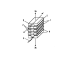
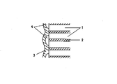
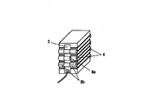
図1は、本発明における積層型圧電セラミックス素子の斜視図であり、図2は、図1のA−A´線断面図の一部である。図1は、例えば、チタン酸ジルコン酸鉛(PZT)、或いはチタン酸バリウムを主成分とする圧電セラミックス材料と銀/パラジウム合金電極材料を用いて、複数の圧電セラミックス層1と複数の内部電極層2を交互に積層してなる積層型圧電セラミックス素子の側面において、露出した前記内部電極層2の端部に対向電極となるように一層置きに絶縁体4を形成し、一層置きに露出している前記内部電極層2の端部は銀の外部電極3に接続し、該外部電極3には外部電源と電気的接続を行うためのリード線6が接続されている。該リード線6に電圧を印加すると、圧電セラミックス層は内部電極間距離で決まる電界強度に応じて変位方向7a−7bの方向に変位する。
【0015】
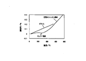
前記圧電セラミックスと従来絶縁層に使用していたガラスの熱膨張率の測定結果を図3に示した。図3から、圧電セラミックスの熱膨張率はキュリー温度前後で変化している。これは、結晶構造の変化による影響であり、圧電セラミックスであれば組成による影響はほとんどなく、キュリー温度に依存する。また、前述のとおり、従来、絶縁層に使用していたガラスの熱膨張率が圧電セラミックスより大きいことが分かる。圧電セラミックス層材料よりも熱膨張率の高いガラスを絶縁層に用いると、冷却中に引張応力が発生しガラスにクラックが生ずるので、絶縁層には圧電セラミッスク層材料と膨張率が同じか低い材料が必要である。
【0016】
また、絶縁層4を圧電セラミックスで形成する場合、焼き付け温度は700℃以上の高温になり、前記絶縁層4が圧電セラミックス層1に拡散し易く、該拡散の影響を回避するためには、前記絶縁層4には前記圧電セラミックス層1と同じ組成、もしくは、前記圧電セラミックス層と同じ元素を含有する組成系の圧電セラミックスを用いる必要がある。
【0017】
また、絶縁層4の焼き付け温度が、圧電セラミックス層1の焼結温度に近い場合、前記圧電セラミックス層1の粒成長や、圧電セラミックスの主成分である鉛が蒸発し、圧電特性が劣化し易いので、圧電セラミックス層の焼結温度よりも100℃以上低温で焼き付けする必要がある。
【0018】
本発明者等は、前記焼き付け温度の低温化を検討結果、絶縁材料の圧電セラミックス粉末の粒子径を1μm以下に微粉末化し、また低融点物質を混合することにより100℃〜200℃焼き付け温度の低温化が可能であることを見出した。
【0019】
図4に、絶縁層形成用の圧電セラミックスの平均粒径をパラメータとして、焼き付け温度と相対密度の測定結果を示した。前記圧電セラミックス粉末の粒子径を1μm以下の微粉末とすることで、圧電セラミックスを100℃以上低温で焼結することができ、平均粒子径0.1μmでは焼き付け温度900℃で緻密な焼結体を形成することができている。
【0020】
また、低融点物質の混合では、圧電セラミックスの圧電特性と絶縁性を劣化させないことが重要であり、ホウケイ酸系ガラス、酸化鉛、ケイ酸鉛、ゲルマニウム酸鉛、ビスマス酸リチウムなどの低融点絶縁物のうち少なくとも1種類を0.1〜20重量%含んだ混合体とすると、鉛系圧電セラミックスの圧電特性を劣化させずに焼き付け温度を100℃以上、下げられることを見出した。表1に、各低融点物質を添加した時の諸特性を示す。
【0021】
【表1】

また、図5には、絶縁層の圧電セラミックスの圧電歪定数d33値が積層型圧電セラミックス素子の圧電セラミックスの圧電歪定数d33値より高い場合の前記絶縁層の破壊モードを示した。絶縁層4を、圧電歪定数d33値が高い圧電セラミックスで形成すると、積層型圧電セラミックス素子に電圧を印加した時に、絶縁層4にクラック8aが発生する。これは、外部電極3の下の絶縁層4は、内部電極層2と外部電極3との間に電界が発生するため圧電効果で変位するが、外部電極3のない部分の絶縁層4は、電界が発生しないため変位せず、その結果、絶縁層4の変位部と非変位部の境界に応力が集中し、クラック8aが発生する。
【0023】
そこで、絶縁層4に用いる圧電セラミックスに圧電セラミックス層1よりも圧電歪定数d33値が95〜60%である低い圧電セラミックス材料を用いることにより、絶縁層4の変位部と非変位部の応力集中を緩和することができ、クラック8aの発生を防止することが可能である。しかし、圧電歪定数d33値が60%以下の圧電セラミックス材料を用いると、図5に示したように、クラック8bが発生するので、本発明の効果が得られず、絶縁層4に用いる圧電セラミックスの圧電歪定数d33値は、圧電セラミックス層1の圧電歪定数d33値の95〜60%であることが必要である。
【0024】
【発明の効果】
以上説明したように、本発明によれば、絶縁層を熱膨張係数の小さい圧電セラミックスで形成することにより、絶縁体層とセラミックス層の境界、またはセラミックス層の変位により生じる絶縁層の応力を低減し、絶縁層とセラミックス層の剥離や絶縁層の破壊を防止し、絶縁性に優れた高信頼性の積層型圧電セラミックス素子を提供することが可能である。
【図面の簡単な説明】
【図1】
本発明の積層型圧電セラミックス素子を示す斜視図。
【図2】
図1中のA−A´線の断面図の一部。
【図3】
圧電セラミックスとガラスの熱膨張率の測定結果を示す図。
【図4】
圧電セラミックスの平均粒径をパラメータとした焼き付け温度と相対密度を示す図。
【図5】圧電歪定数が異なる場合の絶縁層の破壊モードを示す図。
【符号の説明】
1 圧電セラミックス層
2 内部電極層
3 外部電極
4 絶縁層
5 圧電セラミックスの不活性層
6 リード線
7a 変位方向
7b 変位方向
8a 絶縁層のクラック
8b 絶縁層のクラック[0001]
TECHNICAL FIELD OF THE INVENTION
The present invention relates to a multilayer piezoelectric ceramic element used for a multilayer piezoelectric sensor that detects external stress to generate a voltage and a multilayer piezoelectric actuator that generates a displacement or a force by applying a voltage.
[0002]
[Prior art]
2. Description of the Related Art Conventionally, piezoelectric ceramics that generate a voltage by an external stress or deform by application of a voltage have been put to practical use in pressure sensors, piezoelectric actuators, and the like. In recent years, in order to improve the sensitivity of the sensor and the displacement characteristics of the actuator, the piezoelectric ceramic layers and the internal electrode layers are alternately laminated and integrated, and an insulating layer is formed every other layer on the internal electrode layers exposed on the side surfaces of the laminate. A laminated piezoelectric ceramic element having a structure in which a pair of opposed external electrodes connected to the internal electrode layer are formed on the insulating layer is remarkably popular. The main purpose of the insulating layer is to electrically insulate the internal electrode and the external electrode, and it is required that the insulating layer does not break down and does not restrict displacement.
[0003]
With respect to such a structure, there are electrostriction effect elements disclosed as publicly known documents in Japanese Patent Laid-Open Publication No. 59-115579 and Japanese Patent Application Publication No. 2-56830. The electrostrictive effect element has a structure in which an electrostrictive material plate and an internal electrode plate are alternately laminated, and an insulating layer, an organic insulating layer, or a filler is formed only on the exposed portion of the internal electrode layer on the side end surface and on the electrostrictive material in the vicinity thereof. This is a structure in which an organic insulating layer containing is formed, and even if the electrostrictive effect element expands and contracts, no crack occurs in the insulating material and the insulating property and the reliability are high.
[0004]
However, in the above-described electrostrictive effect element, the thickness of the electrostrictive material plate becomes thin, and when the electrostrictive effect element is repeatedly expanded and contracted with a high electric field strength, cracks may occur in the insulating layer, or the insulating layer and the electrostrictive material may be damaged. There was a problem that the layer was peeled off and the insulation was lost.
[0005]
In recent years, the use of laminated piezoelectric ceramic elements in a high-temperature atmosphere of 100 ° C. or higher, such as in an engine room of an automobile or in a high-temperature vapor deposition apparatus, has been increasing, and the thermal expansion coefficient between the piezoelectric ceramic and the insulating layer due to thermal history has increased. Due to this difference, stress is generated at the boundary between the piezoelectric ceramics layer and the insulating layer, and the stress causes cracks in the insulating layer, and the insulating layer and the piezoelectric ceramics layer are separated to lose insulation.
[0006]
[Problems to be solved by the invention]
Therefore, the problem to be solved by the present invention is to reduce the stress generated near the boundary between the ceramic layer and the insulating layer, to prevent peeling and cracking of the ceramic layer and the insulating layer, to provide an excellent insulating property and high reliability. An object of the present invention is to provide a laminated piezoelectric ceramic element.
[0007]
[Means for Solving the Problems]
According to the present invention, a plurality of piezoelectric ceramic layers and internal electrode layers are alternately laminated and integrated to form a laminated body, wherein the internal electrode layer exposed on the side surface of the laminated body serves as a counter electrode. A thermal expansion coefficient of the insulating layer in a laminated piezoelectric ceramic element in which an insulating layer is formed every other layer on the exposed portion of the layer and a pair of external electrodes electrically connected to the exposed portion of the internal electrode layer are formed. Are formed of an insulating material having a coefficient of thermal expansion equal to or less than the thermal expansion coefficient of the piezoelectric ceramic layer.
[0008]
Further, according to the present invention, the material forming the insulating layer is a piezoelectric ceramic, and the piezoelectric ceramic is a piezoelectric ceramic having the same composition as the piezoelectric ceramic layer of the multilayer piezoelectric ceramic element, and A multilayer piezoelectric ceramic device characterized by being a piezoelectric ceramic having a piezoelectric strain constant d33 value of 95 to 60% of the piezoelectric ceramic layer of the piezoelectric ceramic device of the present invention.
[0009]
According to the present invention, the piezoelectric ceramic forming the insulating layer is a baked body of a powder subjected to a low-temperature sintering process, and the particle size of the powder is 1 μm or less. A ceramic element is obtained.
[0010]
Further, according to the present invention, the piezoelectric ceramic powder to be subjected to the low-temperature sintering treatment is a borosilicate glass or at least one of low-melting substances of lead oxide, lead silicate, lead germanate, and lithium bismuthate. A multilayer piezoelectric ceramic element characterized by being a mixture containing 0.1 to 20% by weight is obtained.
[0011]
Normally, the coefficient of thermal expansion of a piezoelectric ceramic used for a laminated piezoelectric ceramic element in a temperature range of 30 ° C. to 500 ° C. is about 40 × 10 −7 / deg, and the insulating layer is made of zinc borosilicate glass or the like. Lead borosilicate glass is used, and the thermal expansion coefficient of the insulating glass in the above temperature range is 40 to 100 × 10 −7 / deg. This difference in the thermal expansion coefficient causes a tensile stress at the boundary between the insulating layer and the ceramic layer due to the thermal history, which causes peeling or cracking of the insulating layer.
[0012]
Therefore, the use of an insulating material having a smaller thermal expansion coefficient than that of the piezoelectric ceramic reduces the tensile stress, prevents separation between the piezoelectric ceramic layer and the insulating layer, prevents breakage of the insulating layer, and displaces the piezoelectric ceramic layer. The stress of the insulating layer caused by the above can be reduced, and breakdown of the insulating layer can be prevented. In addition, by forming the insulating layer of piezoelectric ceramic, the insulating layer is displaced in the same manner as the piezoelectric ceramic layer when a voltage is applied, thereby reducing the stress of the insulating layer caused by the displacement of the ceramic layer and preventing the insulating layer from being broken. Therefore, it is possible to provide a laminated piezoelectric ceramic element having excellent insulation properties and high reliability.
[0013]
BEST MODE FOR CARRYING OUT THE INVENTION
An embodiment of the present invention will be described below with reference to the drawings.
[0014]
FIG. 1 is a perspective view of a laminated piezoelectric ceramic element according to the present invention, and FIG. 2 is a part of a cross-sectional view taken along line AA ′ of FIG. FIG. 1 shows, for example, a plurality of piezoelectric
[0015]
FIG. 3 shows the measurement results of the coefficient of thermal expansion of the piezoelectric ceramic and the glass conventionally used for the insulating layer. From FIG. 3, the coefficient of thermal expansion of the piezoelectric ceramic changes before and after the Curie temperature. This is an effect due to a change in the crystal structure. In the case of piezoelectric ceramics, there is almost no effect due to the composition, and it depends on the Curie temperature. Further, as described above, it can be seen that the thermal expansion coefficient of the glass conventionally used for the insulating layer is larger than that of the piezoelectric ceramic. If glass with a higher coefficient of thermal expansion than the piezoelectric ceramic layer material is used for the insulating layer, a tensile stress will occur during cooling and cracks will occur in the glass, so the insulating layer will have a material with the same or lower expansion coefficient than the piezoelectric ceramic layer material. is necessary.
[0016]
Further, when the
[0017]
Further, when the baking temperature of the insulating
[0018]
The present inventors have studied the lowering of the baking temperature, and as a result, reduced the particle size of the piezoelectric ceramic powder of the insulating material to 1 μm or less, and mixed a low-melting substance to reduce the baking temperature to 100 ° C. to 200 ° C. It has been found that it is possible to lower the temperature.
[0019]
FIG. 4 shows the measurement results of the baking temperature and the relative density using the average particle size of the piezoelectric ceramic for forming the insulating layer as a parameter. By making the particle size of the piezoelectric ceramic powder into a fine powder having a particle size of 1 μm or less, the piezoelectric ceramic can be sintered at a low temperature of 100 ° C. or more. Can be formed.
[0020]
In addition, it is important that the mixing of low-melting substances does not degrade the piezoelectric properties and insulating properties of the piezoelectric ceramics. Low-melting insulating materials such as borosilicate glass, lead oxide, lead silicate, lead germanate, and lithium bismuthate are important. It has been found that when a mixture containing 0.1 to 20% by weight of at least one of the materials is used, the baking temperature can be lowered by 100 ° C. or more without deteriorating the piezoelectric characteristics of the lead-based piezoelectric ceramics. Table 1 shows various properties when each low melting point substance was added.
[0021]
[Table 1]
Further, in FIG. 5, showing the fracture mode of the insulating layer when the piezoelectric strain constant d 33 value of the piezoelectric ceramic of the insulating layer is higher than the piezoelectric strain constant d 33 value of the piezoelectric ceramic of the multilayer piezoelectric ceramic element. The insulating
[0023]
Therefore, by using a lower piezoelectric ceramic material piezoelectric strain constant d 33 value than that of the piezoelectric
[0024]
【The invention's effect】
As described above, according to the present invention, the stress of the insulating layer caused by the boundary between the insulator layer and the ceramic layer or the displacement of the ceramic layer is reduced by forming the insulating layer of the piezoelectric ceramic having a small coefficient of thermal expansion. In addition, it is possible to provide a highly reliable laminated piezoelectric ceramic element having excellent insulating properties by preventing peeling of the insulating layer and the ceramic layer and destruction of the insulating layer.
[Brief description of the drawings]
FIG.
FIG. 1 is a perspective view showing a laminated piezoelectric ceramic element of the present invention.
FIG. 2
FIG. 2 is a part of a cross-sectional view taken along line AA ′ in FIG. 1.
FIG. 3
The figure which shows the measurement result of the coefficient of thermal expansion of piezoelectric ceramics and glass.
FIG. 4
The figure which shows the baking temperature and relative density which made the average particle diameter of the piezoelectric ceramic a parameter.
FIG. 5 is a diagram showing a breakdown mode of an insulating layer when piezoelectric distortion constants are different.
[Explanation of symbols]
REFERENCE SIGNS
Claims (7)
Priority Applications (1)
| Application Number | Priority Date | Filing Date | Title |
|---|---|---|---|
| JP2002165598A JP3946580B2 (en) | 2002-06-06 | 2002-06-06 | Multilayer piezoelectric ceramic element |
Applications Claiming Priority (1)
| Application Number | Priority Date | Filing Date | Title |
|---|---|---|---|
| JP2002165598A JP3946580B2 (en) | 2002-06-06 | 2002-06-06 | Multilayer piezoelectric ceramic element |
Publications (2)
| Publication Number | Publication Date |
|---|---|
| JP2004014777A true JP2004014777A (en) | 2004-01-15 |
| JP3946580B2 JP3946580B2 (en) | 2007-07-18 |
Family
ID=30433399
Family Applications (1)
| Application Number | Title | Priority Date | Filing Date |
|---|---|---|---|
| JP2002165598A Expired - Lifetime JP3946580B2 (en) | 2002-06-06 | 2002-06-06 | Multilayer piezoelectric ceramic element |
Country Status (1)
| Country | Link |
|---|---|
| JP (1) | JP3946580B2 (en) |
-
2002
- 2002-06-06 JP JP2002165598A patent/JP3946580B2/en not_active Expired - Lifetime
Also Published As
| Publication number | Publication date |
|---|---|
| JP3946580B2 (en) | 2007-07-18 |
Similar Documents
| Publication | Publication Date | Title |
|---|---|---|
| EP1732146B1 (en) | Multilayer piezoelectric element | |
| EP1753039B1 (en) | Multilayer piezoelectric element | |
| JP5232167B2 (en) | Piezoceramic multilayer actuator | |
| US8339017B2 (en) | Multi-layer piezoelectric element and injection apparatus using the same | |
| EP1988586B1 (en) | Multi-layer piezoelectric device | |
| JP5522899B2 (en) | Multilayer piezoelectric ceramic actuator and method for manufacturing multilayer piezoelectric ceramic actuator | |
| EP2012374B1 (en) | Multi-layer piezoelectric element | |
| EP1677370B1 (en) | Multilayer piezoelectric device | |
| EP1686633B1 (en) | Multilayer piezoelectric device | |
| JP4802445B2 (en) | Multilayer piezoelectric element and manufacturing method thereof | |
| JP2008270738A (en) | Multilayer piezoceramic actuator and method for manufacturing multilayer piezoceramic actuator | |
| CN100448047C (en) | Laminate type electronic component and production method therefor, laminate type piezoelectric element and jet device | |
| JP2994492B2 (en) | Multilayer piezoelectric actuator and method of manufacturing the same | |
| JP4373643B2 (en) | LAMINATED PIEZOELECTRIC ELEMENT, ITS MANUFACTURING METHOD, AND INJECTION DEVICE | |
| JPH06140683A (en) | Stacked piezoelectric actuator and manufacture thereof | |
| JP2013518422A (en) | Piezoelectric element | |
| JP3946580B2 (en) | Multilayer piezoelectric ceramic element | |
| JP2004103621A (en) | Laminated piezoelectric element | |
| JP2000340849A (en) | Stacked piezoelectric actuator | |
| JP5153095B2 (en) | Multilayer piezoelectric element and jetting apparatus using the same | |
| JP2001102649A (en) | Laminated piezoelectric actuator | |
| JP4158886B2 (en) | Multilayer piezoelectric actuator element | |
| JPH0476969A (en) | Electrostrictive effect element | |
| JP4822664B2 (en) | Multilayer piezoelectric element, manufacturing method thereof, and injection apparatus | |
| JP4997942B2 (en) | Piezoelectric element |
Legal Events
| Date | Code | Title | Description |
|---|---|---|---|
| A977 | Report on retrieval |
Free format text: JAPANESE INTERMEDIATE CODE: A971007 Effective date: 20050502 |
|
| A131 | Notification of reasons for refusal |
Free format text: JAPANESE INTERMEDIATE CODE: A131 Effective date: 20070110 |
|
| A521 | Request for written amendment filed |
Free format text: JAPANESE INTERMEDIATE CODE: A523 Effective date: 20070307 |
|
| TRDD | Decision of grant or rejection written | ||
| A01 | Written decision to grant a patent or to grant a registration (utility model) |
Free format text: JAPANESE INTERMEDIATE CODE: A01 Effective date: 20070404 |
|
| A61 | First payment of annual fees (during grant procedure) |
Free format text: JAPANESE INTERMEDIATE CODE: A61 Effective date: 20070411 |
|
| R150 | Certificate of patent or registration of utility model |
Ref document number: 3946580 Country of ref document: JP Free format text: JAPANESE INTERMEDIATE CODE: R150 Free format text: JAPANESE INTERMEDIATE CODE: R150 |
|
| FPAY | Renewal fee payment (event date is renewal date of database) |
Free format text: PAYMENT UNTIL: 20110420 Year of fee payment: 4 |
|
| FPAY | Renewal fee payment (event date is renewal date of database) |
Free format text: PAYMENT UNTIL: 20120420 Year of fee payment: 5 |
|
| FPAY | Renewal fee payment (event date is renewal date of database) |
Free format text: PAYMENT UNTIL: 20120420 Year of fee payment: 5 |
|
| FPAY | Renewal fee payment (event date is renewal date of database) |
Free format text: PAYMENT UNTIL: 20130420 Year of fee payment: 6 |
|
| FPAY | Renewal fee payment (event date is renewal date of database) |
Free format text: PAYMENT UNTIL: 20130420 Year of fee payment: 6 |
|
| FPAY | Renewal fee payment (event date is renewal date of database) |
Free format text: PAYMENT UNTIL: 20140420 Year of fee payment: 7 |
|
| S533 | Written request for registration of change of name |
Free format text: JAPANESE INTERMEDIATE CODE: R313533 |
|
| R350 | Written notification of registration of transfer |
Free format text: JAPANESE INTERMEDIATE CODE: R350 |
|
| R250 | Receipt of annual fees |
Free format text: JAPANESE INTERMEDIATE CODE: R250 |
|
| R250 | Receipt of annual fees |
Free format text: JAPANESE INTERMEDIATE CODE: R250 |
|
| R250 | Receipt of annual fees |
Free format text: JAPANESE INTERMEDIATE CODE: R250 |
|
| EXPY | Cancellation because of completion of term |