JP2004001227A - Device and method for polishing - Google Patents
Device and method for polishing Download PDFInfo
- Publication number
- JP2004001227A JP2004001227A JP2003276542A JP2003276542A JP2004001227A JP 2004001227 A JP2004001227 A JP 2004001227A JP 2003276542 A JP2003276542 A JP 2003276542A JP 2003276542 A JP2003276542 A JP 2003276542A JP 2004001227 A JP2004001227 A JP 2004001227A
- Authority
- JP
- Japan
- Prior art keywords
- polishing
- polished
- film thickness
- turntable
- detecting means
- Prior art date
- Legal status (The legal status is an assumption and is not a legal conclusion. Google has not performed a legal analysis and makes no representation as to the accuracy of the status listed.)
- Withdrawn
Links
Images


Abstract
Description
本発明はポリッシング装置および方法に係り、特に半導体ウエハ等の被研磨物を研磨する際、被研磨物をトップリングに装着した状態で該被研磨物の研磨面を露出させることなく、被研磨物の膜厚をリアルタイムで連続的に検出することができるポリッシング装置および方法に関するものである。 The present invention relates to a polishing apparatus and method, particularly when polishing an object to be polished such as a semiconductor wafer, without exposing a polished surface of the object to be polished while the object to be polished is mounted on a top ring. The present invention relates to a polishing apparatus and a polishing method capable of continuously detecting the film thickness in real time.
近年、半導体デバイスの高集積化が進むにつれて回路の配線が微細化し、配線間距離もより狭くなりつつある。特に、0.5μm以下の光リソグラフィの場合は、焦点深度が浅くなるため、ステッパーの結像面の平坦度を必要とする。そこで、半導体ウエハ表面を平坦化することが必要となるが、この平坦化法の1手段として半導体ウエハの表面をポリッシング装置で研磨することが行われている。 、 In recent years, as the degree of integration of semiconductor devices has increased, circuit wiring has become finer, and the distance between wirings has become smaller. In particular, in the case of optical lithography of 0.5 μm or less, since the depth of focus becomes shallow, a flatness of the image formation surface of the stepper is required. Therefore, it is necessary to flatten the surface of the semiconductor wafer. As one of the flattening methods, the surface of the semiconductor wafer is polished by a polishing apparatus.
この種のポリッシング装置は、対向し各々独立して回転するターンテーブルとトップリングを具備し、トップリングが一定の圧力をターンテーブルに与え、ターンテーブルとトップリングの間に半導体ウエハを介在させて、該半導体ウエハの表面を平坦かつ鏡面に研磨している。 This type of polishing apparatus is provided with a turntable and a top ring which face each other and rotate independently, the top ring applies a constant pressure to the turntable, and a semiconductor wafer is interposed between the turntable and the top ring. The surface of the semiconductor wafer is polished flat and mirror-finished.
上記のようなポリッシング装置を用いて半導体ウエハを研磨する場合の問題点は、半導体ウエハの研磨面が所望の平坦度又は厚さに研磨されているかどうかを決定することにある。例えば、半導体ウエハ上に蒸着層を形成し、その上に種々の集積回路素子を形成し、酸化物材料の厚さを取り除きたいことがよくある。この酸化物材料の取り除きあるいは平坦化する際に、素子のどの部分も取り除くことなく、酸化物を種々の集積回路素子の頂部まで取り除くことが望ましい。 A problem when polishing a semiconductor wafer using the above polishing apparatus is to determine whether the polished surface of the semiconductor wafer is polished to a desired flatness or thickness. For example, it is often desirable to form a vapor deposited layer on a semiconductor wafer, form various integrated circuit elements thereon, and remove the thickness of the oxide material. In removing or planarizing this oxide material, it is desirable to remove the oxide to the top of various integrated circuit devices without removing any portion of the device.
従来、この平坦化のプロセスは、ターンテーブルとトップリングの回転速度、トップリングのターンテーブルに与える圧力、化学的スラリー及び平坦化プロセスの時間を制御することによって行われていた。そして、半導体ウエハの被研磨面の膜厚、平坦度等は、ポリッシング装置から半導体ウエハを機械的に取り外し、当該技術分野で公知の方法によって物理的に測定することによって確認していた。 Traditionally, this planarization process has been performed by controlling the rotation speed of the turntable and top ring, the pressure applied to the top ring turntable, the chemical slurry, and the time of the planarization process. The thickness, flatness, and the like of the polished surface of the semiconductor wafer were confirmed by mechanically removing the semiconductor wafer from the polishing apparatus and physically measuring the semiconductor wafer by a method known in the art.
ここで、ウエハが仕様に適合しない場合、当該ウエハをポリッシング装置に戻し、更に2度目の平坦化研磨工程を行っていた。即ち、研磨面の膜厚を検出するためには、ポリッシング装置から半導体ウエハを取り外し、更に研磨不足の場合は再び半導体ウエハをポリッシング装置にセットするという作業の反復が必要となり、この作業に費やす時間及び労力が問題となっていた。 Here, when the wafer does not conform to the specifications, the wafer is returned to the polishing apparatus, and the second flattening and polishing step is performed. That is, in order to detect the film thickness of the polished surface, it is necessary to repeat the work of removing the semiconductor wafer from the polishing apparatus and setting the semiconductor wafer again in the polishing apparatus when polishing is insufficient, and the time required for this work is required. And labor was a problem.
この問題に対して、半導体ウエハをトップリングに装着したまま、研磨途中にトップリングをターンテーブル外にずらして被研磨面を露出させた状態で膜厚を検出する方法が提案されている。この方法によれば、上記の時間及び労力の問題は大幅に解消されることになるが、膜厚を検出するには、一時的にトップリングをターンテーブル外にずらす工程が必要となるため、リアルタイムでの膜厚検出が不可能であること、また研磨時間が長くなるなどの問題がある。 To solve this problem, a method has been proposed in which the top ring is shifted out of the turntable during polishing while the semiconductor wafer is mounted on the top ring, and the film thickness is detected in a state where the surface to be polished is exposed. According to this method, the above-described problem of time and labor is largely solved.However, in order to detect the film thickness, a step of temporarily moving the top ring out of the turntable is required. There are problems such as the inability to detect the film thickness in real time and the increase in polishing time.
本発明は上述の事情に鑑みなされたもので、半導体ウエハをトップリングに装着したまま、該トップリングをターンテーブル外にずらすことなく、被研磨面の膜厚をリアルタイムで検出できるポリッシング装置および方法を提供することを目的とする。 The present invention has been made in view of the above circumstances, and has a polishing apparatus and method capable of detecting the thickness of a surface to be polished in real time without displacing the top ring out of a turntable while the semiconductor wafer is mounted on the top ring. The purpose is to provide.
上述した目的を達成するため、本発明のポリッシング装置の一態様は、ターンテーブルと、被研磨物を保持するトップリングとを有し、該トップリングによって保持された該被研磨物を該ターンテーブルの上面に押圧して該被研磨物の被研磨面を研磨するポリッシング装置であって、前記ターンテーブル内には前記被研磨面の膜厚を検出する複数の膜厚検出手段が配置され、前記複数の膜厚検出手段は連続的に前記被研磨面の膜厚検出を行うことを特徴とするものである。 In order to achieve the above-described object, one embodiment of the polishing apparatus of the present invention includes a turntable and a top ring for holding an object to be polished, wherein the object to be polished held by the top ring is attached to the turntable. A polishing apparatus for pressing the upper surface of the object to polish the surface to be polished of the object to be polished, wherein a plurality of film thickness detecting means for detecting the film thickness of the surface to be polished are arranged in the turntable, The plurality of film thickness detecting means continuously detects the film thickness of the surface to be polished.
前記ポリッシング装置は更に、前記ターンテーブルの上面に張り付けられ、前記被研磨面を研磨する研磨布を有し、前記研磨布は前記ターンテーブル内の膜厚検出手段の位置に対応して少なくとも一つの開孔部を有していることを特徴とする。
前記複数の膜厚検出手段は同時に前記被研磨面の膜厚検出を行うことを特徴とする。
前記複数の膜厚検出手段の少なくとも一つは光学式膜厚検出手段であることを特徴とする。
The polishing apparatus further includes a polishing cloth attached to an upper surface of the turntable and polishing the surface to be polished, wherein the polishing cloth has at least one polishing cloth corresponding to a position of a film thickness detecting means in the turntable. It is characterized by having an opening.
The plurality of film thickness detecting means may simultaneously detect the film thickness of the surface to be polished.
At least one of the plurality of film thickness detecting means is an optical film thickness detecting means.
本発明のポリッシング方法の一態様は、ターンテーブルとトップリングを有するポリッシング装置内にて、該ターンテーブルの研磨面に、該トップリングで保持した被研磨物を押圧し、該被研磨物の被研磨面を研磨するポリッシング方法であって、前記被研磨面の膜厚を複数の膜厚検出手段で検出し、該複数の膜厚検出手段から得られた強度を演算部にて算出し、前記算出された強度の加算値から膜厚を検出することを特徴とするものである。 In one embodiment of the polishing method of the present invention, in a polishing apparatus having a turntable and a top ring, an object to be polished held by the top ring is pressed against a polishing surface of the turntable, and the object to be polished is polished. A polishing method for polishing a polished surface, wherein the film thickness of the polished surface is detected by a plurality of film thickness detecting means, and the intensity obtained from the plurality of film thickness detecting means is calculated by an arithmetic unit, The film thickness is detected from the sum of the calculated intensities.
前記算出された強度の加算値から検出された前記膜厚をもとに前記ポリッシング装置の運転条件を制御することを特徴とする。
前記複数の膜厚検出手段は、同時に前記被研磨面の膜厚を検出することを特徴とする。
前記複数の膜厚検出手段は、連続的に前記被研磨面の膜厚を検出することを特徴とする。
前記加算値と、予め記憶されている初期値との差分から、研磨速度を算出し、該研磨速度から研磨の運転操作条件を制御することを特徴とする。
The operating condition of the polishing apparatus is controlled based on the film thickness detected from the sum of the calculated intensities.
The plurality of film thickness detecting means simultaneously detects the film thickness of the surface to be polished.
The plurality of film thickness detecting means continuously detects the film thickness of the surface to be polished.
A polishing speed is calculated from a difference between the added value and a previously stored initial value, and a polishing operation condition is controlled based on the polishing speed.
本発明のポリッシング装置の他の態様は、ターンテーブルと、被研磨物を保持する保持具とを有し、該保持具によって保持された該被研磨物を該ターンテーブルの上面に押圧して該被研磨物の被研磨面を研磨するポリッシング装置であって、前記ターンテーブルは該ターンテーブルの上面に張り付けられる研磨布を有し、前記研磨布には一部にシール材料が設けられ、該シール材料は研磨能力の低い材料であることを特徴とするものである。 Another embodiment of the polishing apparatus of the present invention has a turntable and a holder for holding the object to be polished, and presses the object to be polished held by the holder against the upper surface of the turntable to form the polishing object. A polishing apparatus for polishing a surface to be polished of an object to be polished, wherein the turntable has a polishing cloth attached to an upper surface of the turntable, wherein the polishing cloth is provided with a sealing material in a part thereof, The material is characterized by having a low polishing ability.
前記被研磨面の膜厚を測定するための膜厚検出手段を有することを特徴とする。
前記膜厚検出手段は、前記ターンテーブル内に設けられていることを特徴とする。
前記研磨布は、前記複数の膜厚検出手段が配置されている位置に対応して開孔部を有することを特徴とする。
前記膜厚検出手段は、投光部と受光部を有し、前記シール材料は、前記投光部と前記受光部が配置された部分に設けられていることを特徴とする。
It is characterized by having a film thickness detecting means for measuring the film thickness of the surface to be polished.
The film thickness detecting means is provided in the turntable.
The polishing pad has an opening corresponding to a position where the plurality of film thickness detecting means are arranged.
The film thickness detecting means has a light projecting portion and a light receiving portion, and the sealing material is provided at a portion where the light projecting portion and the light receiving portion are arranged.
本発明のポリッシング方法の他の態様は、ターンテーブルとトップリングを有するポリッシング装置内にて、該ターンテーブルの研磨面に、該トップリングで保持した被研磨物を押圧し、該被研磨物の被研磨面を研磨するポリッシング方法であって、前記被研磨面の半径位置が異なる複数点の膜厚時間変化を膜厚検出手段で検出し、該被研磨面の研磨プロファイルを被研磨面の背後からの圧力を用いて研磨中に制御することを特徴とするものである。 Another aspect of the polishing method of the present invention is that, in a polishing apparatus having a turntable and a top ring, an object to be polished held by the top ring is pressed against a polishing surface of the turntable, and A polishing method for polishing a surface to be polished, wherein a change in film thickness with time at a plurality of points at different radial positions of the surface to be polished is detected by a film thickness detecting means, and a polishing profile of the surface to be polished is measured behind the surface to be polished. The polishing is controlled during polishing using pressure from
本発明のポリッシング方法の他の態様は、ターンテーブルとトップリングを有するポリッシング装置内にて、該ターンテーブルの研磨面に、該トップリングで保持した被研磨物を押圧し、該被研磨物の被研磨面を研磨するポリッシング方法であって、前記被研磨面の特定点の膜厚時間変化を膜厚検出手段で検出し、研磨条件を研磨中に制御することを特徴とするものである。 Another aspect of the polishing method of the present invention is that, in a polishing apparatus having a turntable and a top ring, an object to be polished held by the top ring is pressed against a polishing surface of the turntable, and A polishing method for polishing a surface to be polished, characterized in that a change in film thickness with time at a specific point on the surface to be polished is detected by a film thickness detecting means, and polishing conditions are controlled during polishing.
本発明のポリッシング装置の好ましい態様は、対向し各々独立して回転するトップリングと研磨布を備えたターンテーブルを具備し、該ターンテーブルとトップリングの間に板状の被研磨物を介在させ、所定の力で該被研磨物を押圧し、該被研磨物の表面を研磨するポリッシング装置において、前記ターンテーブル上のトップリングの軌道上に、前記被研磨物の被研磨面に光を投光する投光部と該被研磨面で反射する光を受光する受光部とからなるセンサを具備した被研磨物膜厚検出手段を設け、前記トップリングに該被研磨物を装着した状態で該被研磨物を露出させることなく、前記受光部で受光する反射光から、研磨中の該被研磨物の膜厚をリアルタイムで連続的に検出することを可能にした。 A preferred embodiment of the polishing apparatus of the present invention includes a turntable having a top ring and a polishing cloth opposed to each other and independently rotating, and a plate-shaped object to be polished is interposed between the turntable and the top ring. In a polishing apparatus for pressing the object to be polished with a predetermined force and polishing the surface of the object to be polished, light is projected onto the surface to be polished of the object to be polished on a track of a top ring on the turntable. An object to be polished film thickness detecting means provided with a sensor comprising a light projecting portion that emits light and a light receiving portion that receives light reflected by the surface to be polished is provided, and the object to be polished is mounted on the top ring. Without exposing the object to be polished, the thickness of the object to be polished can be continuously detected in real time from the reflected light received by the light receiving section.
前記被研磨物膜厚検出手段は、被研磨物膜厚を前記受光部によって受光された光の反射光強度の変化より検出してもよい。 The thickness of the object to be polished may be detected from a change in the intensity of the reflected light of the light received by the light receiving section.
前記研磨物膜厚検出手段は、投光部と受光部とからなるセンサをターンテーブル上の半径方向に複数個配置して構成し、被研磨物の被研磨面全面の膜厚を同時にリアルタイムで検出可能としてもよい。 The polishing object film thickness detecting means is configured by arranging a plurality of sensors each including a light projecting unit and a light receiving unit in a radial direction on a turntable, and simultaneously measuring the film thickness of the entire surface of the object to be polished in real time. It may be detectable.
前記被研磨物膜厚検出手段は、前記ターンテーブルの中心と外周の弧によって囲まれる、前記センサを含む領域については、研磨能力の極めて低い研磨布あるいは研磨能力を有しない材料を設けてもよい。 The object-to-be-polished film thickness detecting means may be provided with a polishing cloth having an extremely low polishing ability or a material having no polishing ability in a region including the sensor, which is surrounded by the arc of the center and the outer periphery of the turntable. .
前記被研磨物膜厚検出手段は、前記受光部で受光した受光信号を増幅する増幅部と、該増幅部で増幅された受光信号からノイズを除去するアナログフィルタと、該ノイズが除去された受光信号をデジタル信号に変換するA/D変換部と、該デジタル信号化された前記受光信号と初期値との差の絶対値を算出し、該差の絶対値と所定の闘値とを比較演算する演算部からなるようにしてもよい。 The polished object film thickness detecting means includes an amplifier for amplifying a light reception signal received by the light receiver, an analog filter for removing noise from the light reception signal amplified by the amplifier, and a light receiver for removing the noise. An A / D converter for converting a signal into a digital signal; calculating an absolute value of a difference between the digitalized light receiving signal and an initial value; and comparing the absolute value of the difference with a predetermined threshold value It may be made up of an arithmetic unit that performs the calculation.
本発明は上記構成を採用することにより、研磨中に、投光部から該研磨面に光を投射し、該被研磨物で反射する光を受光部で受光し、該受光部で受光する反射光から該被研磨物の膜厚をリアルタイムで、かつ連続的に自動検出できる。したがって、従来のように、被研磨物の膜厚を検出するたびに被研磨物をトップリングから取り外す必要がないのは勿論、研磨途中で、トップリングをターンテーブル外までずらす必要もない。 The present invention adopts the above configuration, during polishing, projects light from the light projecting portion to the polishing surface, receives light reflected by the object to be polished by the light receiving portion, and receives light reflected by the light receiving portion. The thickness of the object to be polished can be automatically detected in real time and continuously from the light. Therefore, unlike the related art, it is not necessary to remove the object to be polished from the top ring every time the thickness of the object to be polished is detected, and it is not necessary to shift the top ring to outside the turntable during polishing.
本発明によれば、研磨中に、投光部から被研磨物の研磨面に光を投射し、被研磨面で反射する光を受光部で受光し、該受光部で受光する反射光から被研磨物の膜厚をリアルタイムで、かつ連続的に自動検出できる。したがって、従来のように、被研磨物の膜厚を検出するたびに被研磨物をトップリングから取り外す必要がないのは勿論、研磨途中で、トップリングをターンテーブル外までずらす必要もない。 According to the present invention, during polishing, light is projected from the light projecting portion to the polished surface of the object to be polished, light reflected on the surface to be polished is received by the light receiving portion, and light is reflected from the reflected light received by the light receiving portion. The film thickness of the polished object can be automatically detected in real time and continuously. Therefore, unlike the related art, it is not necessary to remove the object to be polished from the top ring every time the thickness of the object to be polished is detected, and it is not necessary to shift the top ring to outside the turntable during polishing.
以下、本発明に係るポリッシング装置の実施例を図面に基づいて説明する。本実施例においては、被研磨物として半導体ウエハを例に挙げて説明する。
図1は、本発明のポリッシング装置の全体構成を示す縦断面図である。図1に示されるように、ポリッシング装置は、ターンテーブル1と、半導体ウエハ2を保持しつつターンテーブル1に押付けるトップリング3とを具備している。前記ターンテーブル1はモータ(図示せず)に連結されており、矢印で示すようにその軸心まわりに回転可能になっている。また、ターンテーブル1の上面には、研磨布4が貼設されている。
Hereinafter, embodiments of a polishing apparatus according to the present invention will be described with reference to the drawings. In this embodiment, a semiconductor wafer will be described as an example of the object to be polished.
FIG. 1 is a longitudinal sectional view showing the overall configuration of the polishing apparatus of the present invention. As shown in FIG. 1, the polishing apparatus includes a turntable 1 and a
また、トップリング3は、モータ(図示せず)に連結されるとともに昇降シリンダ(図示せず)に連結されている。これによって、トップリング3は、矢印で示すように昇降可能かつその軸心まわりに回転可能になっており、半導体ウエハ2を研磨布4に対して任意の圧力で押圧することができるようになっている。なお、トップリング3の下部外周部には、半導体ウエハ2の外れ止めを行うガイドリング6が設けられている。
また、ターンテーブル1の上方には研磨砥液ノズル5が設置されており、研磨砥液ノズル5によってターンテーブル1に張り付けられた研磨布4上に研磨砥液Qが供給されるようになっている。
The
A polishing abrasive
上記構成のポリッシング装置において、トップリング3の下面に半導体ウエハ2を保持させ、半導体ウエハ2を回転しているターンテーブル1の上面の研磨布4に昇降シリンダにより押圧する。一方、研磨砥液ノズル5から研磨砥液Qを流すことにより、研磨布4に研磨砥液Qが保持されており、半導体ウエハ2の研磨される面(下面)と研磨布4の間に研磨砥液Qが存在した状態でポリッシングが行われる。
In the polishing apparatus having the above structure, the
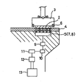
図2は本発明のポリッシング装置の要部詳細を示す図である。半導体ウエハ2には基板の表面にSiO2からなる酸化膜が形成されている。ポリッシング装置は、酸化膜の膜厚を研磨中に測定するための膜厚検出手段を備えている。トップリング3は研磨終了時点まで、半導体ウエハ2の被研磨面の全体がターンテーブル1の上面、すなわち研磨布4で覆われた状態となるような位置をとり、この状態のままで、膜厚検出手段によって、研磨中の被研磨面の酸化膜の膜厚をリアルタイムで、かつ連続的に検出する。
FIG. 2 is a diagram showing details of a main part of the polishing apparatus of the present invention. On the
膜厚検出手段は、図2に示すように半導体ウエハ2の被研磨面に光を投光する投光部7と被研磨面で反射する光を受光する受光部8とからなるセンサS、増幅部9、アナログフィルタ10、A/D変換部11、演算部12、制御部13を備えている。投光部7及び受光部8からなるセンサSはターンテーブル1上のトップリング3の軌道上に配置されており、かつ研磨布4の下方でターンテーブル1の内部に設けられている。センサSの投光部7及び受光部8は、それぞれ単一あるいは複数の投光素子、受光素子を具備し、該投光素子の各々から半導体ウエハ2の被研磨面に光を照射し、各々の反射光は受光素子で受光する。また、研磨布4には、センサSの光を通過させるように孔が設けられている。
As shown in FIG. 2, the film thickness detecting means includes a sensor S including a light projecting unit 7 for projecting light on the surface to be polished of the
なお、センサSの投光部7及び受光部8は、半導体ウエハ2の中心の位置する軌道上に配置すれば1組だけで、半導体ウエハ2の移動に伴なって被研磨面全面の膜厚検出が可能である。ただし、この場合は、検出時刻に多少のタイムラグが生ずるため、同一時刻での検出が必要とされる場合は、複数組の投光部7、受光部8が必要となる。
In addition, if the light projecting unit 7 and the light receiving unit 8 of the sensor S are arranged on a track located at the center of the
受光部8で受光された反射光は、各々の強度に比例した電気信号に変換されて増幅部9によって一定倍率で増幅され、アナログフィルタ10を通ってノイズが除去される。次に、各々の電気信号がA/D変換部11に送られ、アナログ信号がデジタル信号に変換され、一定間隔の信号としてサンプリングされる。
(4) The reflected light received by the light receiving unit 8 is converted into an electric signal proportional to each intensity, amplified by the amplification unit 9 at a fixed magnification, and passed through the
次に、各々のデジタル信号を演算部12に入力し、該演算部12で各々の信号の強度を算出し、各々の強度を加算して加算値を得る。この加算値から半導体ウエハ2の被研磨面の膜厚が算出される。また、該加算値と、予め記憶されている初期値(研磨開始前の反射光強度の加算値、即ち初期加算値)と比較演算し、加算値と初期値との差分絶対値から、研磨速度が算定される。ここで得られた、被研磨面全面の膜厚、研磨速度をもとにポリッシング装置の運転条件を演算し、この演算結果を制御部13に送り、ポリッシング装置の運転操作条件を制御し、被研磨面の平坦度向上をはかる。また、半導体ウエハの被研磨面上の各点で測定された膜厚を比較することによって被研磨面の平坦度を知ることができる。
Next, each digital signal is input to the
半導体ウエハ上の特定点の膜厚を時間経過に対して測定することで、研磨中の研磨速度の時間変化を捕らえることができる。この情報を用いれば、研磨条件(圧力、回転数など)を制御して、一定研磨速度を実現することが可能になるほか、研磨布の寿命の判定や予測や、適正なドレッシング条件の割り出しも可能となる。また半導体ウエハ上の半径位置が異なる複数の測定点の膜厚の時間変化を用いれば、ウエハの研磨プロファイルをバックサイドプレッシャーなどを用いて、研磨中に制御することも可能となる。 (4) By measuring the film thickness at a specific point on the semiconductor wafer with respect to the passage of time, it is possible to capture a change in polishing rate with time during polishing. Using this information, it is possible to control the polishing conditions (pressure, number of revolutions, etc.) to achieve a constant polishing rate, to determine and predict the life of the polishing cloth, and to determine appropriate dressing conditions. It becomes possible. Further, by using the time change of the film thickness at a plurality of measurement points having different radial positions on the semiconductor wafer, the polishing profile of the wafer can be controlled during polishing by using a backside pressure or the like.
また検出された膜厚が所定の膜厚にほぼ一致した時点で研磨動作を終了するようにポリッシング装置を制御することができる。
さらに検出された平坦度が所定の平坦度にほぼ一致した時点で研磨動作を終了するようにポリッシング装置を制御することができる。
Further, the polishing apparatus can be controlled so that the polishing operation is finished when the detected film thickness substantially matches the predetermined film thickness.
Further, the polishing apparatus can be controlled so as to end the polishing operation when the detected flatness substantially matches the predetermined flatness.
図3にターンテーブル1内に投光部7及び受光部8からなるセンサSを埋め込み配置した場合を示す。図3(a)は平面図、図3(b)は部分断面図である。半導体ウエハ2の中心の位置する軌道14上に該投光部7、受光部8を配置することで、1組のみで被研磨面全面の膜厚検出が可能である。ただし、この場合は、ウエハ面上を一定時間内で移動しながら膜厚を検出していくため、各膜厚の検出時刻に多少のタイムラグが生ずる。従って同一時刻での検出が必要な場合は、投光部7、受光部8からなるセンサSを複数個配置する必要がある。
FIG. 3 shows a case where the sensor S including the light projecting unit 7 and the light receiving unit 8 is embedded and arranged in the turntable 1. FIG. 3A is a plan view, and FIG. 3B is a partial sectional view. By arranging the light projecting unit 7 and the light receiving unit 8 on the
図4はターンテーブルの半径方向に複数のセンサSを配置した場合を示す図であり、図4(a)は平面図、図4(b)は部分断面図である。複数のセンサSは半径方向に所定間隔をおいて配置されている。この場合、いずれのセンサSも半導体ウエハ2の軌道内に位置している。
また、ターンテーブル1内に投光部7、受光部8を埋め込み配置した場合は、その領域には研磨布4が存在しないため、研磨布4全面でみると、半導体ウエハ2の研磨面に対する研磨強度にムラが生ずることになる。これを是正するために図3及び図4に示すように該投光部7、受光部8が配置された部分を含む、研磨布4の斜線部分(ターンテーブル中心Oと外周の弧によって囲まれる部分)Aの領域については、研磨能力の極めて低い研磨布または研磨能力を有しない材料(シール状のテープなど)を設けることとする。
4A and 4B are diagrams showing a case where a plurality of sensors S are arranged in the radial direction of the turntable. FIG. 4A is a plan view, and FIG. 4B is a partial sectional view. The plurality of sensors S are arranged at predetermined intervals in the radial direction. In this case, all the sensors S are located in the trajectory of the
When the light emitting unit 7 and the light receiving unit 8 are embedded in the turntable 1, the polishing
次の方法によって酸化膜の膜厚を測定することもできる。即ち、投光部から半導体ウエハに入射した光は、酸化膜に入射し、膜の上下面で反射する。この膜の上下面で反射した反射光は互いに干渉して干渉色を生ずる。この干渉色を受光部で測光することにより酸化膜の厚さを測定することができる。
尚、実施例においては、半導体ウエハの表面に形成される膜を酸化膜を例に挙げて説明したが、膜の種類は酸化膜に限られない。
The thickness of the oxide film can be measured by the following method. That is, the light incident on the semiconductor wafer from the light projecting part enters the oxide film and is reflected on the upper and lower surfaces of the film. The reflected lights reflected on the upper and lower surfaces of this film interfere with each other to generate an interference color. The thickness of the oxide film can be measured by measuring the interference color with the light receiving unit.
In the embodiments, the film formed on the surface of the semiconductor wafer has been described using an oxide film as an example, but the type of the film is not limited to the oxide film.
1 ターンテーブル
2 半導体ウエハ
3 トップリング
4 研磨布
5 研磨液ノズル
6 ガイドリング
S センサ
7 投光部
8 受光部
9 増幅部
10 アナログフィルタ
11 A/D変換部
12 演算部
13 制御部
DESCRIPTION OF SYMBOLS 1
Claims (16)
被研磨物を保持するトップリングとを有し、
該トップリングによって保持された該被研磨物を該ターンテーブルの上面に押圧して該被研磨物の被研磨面を研磨するポリッシング装置であって、
前記ターンテーブル内には前記被研磨面の膜厚を検出する複数の膜厚検出手段が配置され、
前記複数の膜厚検出手段は連続的に前記被研磨面の膜厚検出を行うことを特徴とするポリッシング装置。 Turntable,
And a top ring for holding the object to be polished,
A polishing apparatus for pressing the object to be polished held by the top ring against the upper surface of the turntable to polish the surface to be polished of the object to be polished,
A plurality of film thickness detecting means for detecting the film thickness of the surface to be polished is arranged in the turntable,
The polishing apparatus according to claim 1, wherein the plurality of film thickness detecting means continuously detect the film thickness of the surface to be polished.
前記研磨布は前記ターンテーブル内の膜厚検出手段の位置に対応して少なくとも一つの開孔部を有していることを特徴とする請求項1記載のポリッシング装置。 The polishing apparatus further includes a polishing cloth attached to the upper surface of the turntable, and polishing the surface to be polished,
2. The polishing apparatus according to claim 1, wherein the polishing cloth has at least one opening corresponding to a position of the film thickness detecting means in the turntable.
該ターンテーブルの研磨面に、該トップリングで保持した被研磨物を押圧し、
該被研磨物の被研磨面を研磨するポリッシング方法であって、
前記被研磨面の膜厚を複数の膜厚検出手段で検出し、
該複数の膜厚検出手段から得られた強度を演算部にて算出し、前記算出された強度の加算値から膜厚を検出することを特徴とするポリッシング方法。 In a polishing machine with a turntable and a top ring,
The object to be polished held by the top ring is pressed against the polishing surface of the turntable,
A polishing method for polishing a surface to be polished of the object to be polished,
The film thickness of the polished surface is detected by a plurality of film thickness detecting means,
A polishing method, comprising: calculating intensities obtained from the plurality of film thickness detecting means in a calculation unit; and detecting a film thickness from an added value of the calculated intensities.
前記ターンテーブルは該ターンテーブルの上面に張り付けられる研磨布を有し、前記研磨布には一部にシール材料が設けられ、該シール材料は研磨能力の低い材料であることを特徴とするポリッシング装置。 Polishing, having a turntable and a holder for holding the object to be polished, pressing the object to be polished held by the holder against the upper surface of the turntable to polish the surface to be polished of the object to be polished A device,
The polishing apparatus, wherein the turntable has a polishing cloth attached to an upper surface of the turntable, and the polishing cloth is partially provided with a sealing material, and the sealing material is a material having a low polishing ability. .
該ターンテーブルの研磨面に、該トップリングで保持した被研磨物を押圧し、
該被研磨物の被研磨面を研磨するポリッシング方法であって、
前記被研磨面の半径位置が異なる複数点の膜厚時間変化を膜厚検出手段で検出し、
該被研磨面の研磨プロファイルを被研磨面の背後からの圧力を用いて研磨中に制御することを特徴とするポリッシング方法。 In a polishing machine with a turntable and a top ring,
The object to be polished held by the top ring is pressed against the polishing surface of the turntable,
A polishing method for polishing a surface to be polished of the object to be polished,
The film thickness detecting means detects a time-dependent change in film thickness at a plurality of points at different radial positions of the polished surface,
A polishing method, wherein a polishing profile of the surface to be polished is controlled during polishing by using a pressure from behind the surface to be polished.
該ターンテーブルの研磨面に、該トップリングで保持した被研磨物を押圧し、
該被研磨物の被研磨面を研磨するポリッシング方法であって、
前記被研磨面の特定点の膜厚時間変化を膜厚検出手段で検出し、
研磨条件を研磨中に制御することを特徴とするポリッシング方法。 In a polishing machine with a turntable and a top ring,
The object to be polished held by the top ring is pressed against the polishing surface of the turntable,
A polishing method for polishing a surface to be polished of the object to be polished,
A change in film thickness with time at a specific point on the surface to be polished is detected by a film thickness detecting means,
A polishing method, wherein polishing conditions are controlled during polishing.
Priority Applications (1)
| Application Number | Priority Date | Filing Date | Title |
|---|---|---|---|
| JP2003276542A JP2004001227A (en) | 1995-07-20 | 2003-07-18 | Device and method for polishing |
Applications Claiming Priority (2)
| Application Number | Priority Date | Filing Date | Title |
|---|---|---|---|
| JP20659395 | 1995-07-20 | ||
| JP2003276542A JP2004001227A (en) | 1995-07-20 | 2003-07-18 | Device and method for polishing |
Related Parent Applications (1)
| Application Number | Title | Priority Date | Filing Date |
|---|---|---|---|
| JP20881496A Division JP3601910B2 (en) | 1995-07-20 | 1996-07-19 | Polishing apparatus and method |
Related Child Applications (2)
| Application Number | Title | Priority Date | Filing Date |
|---|---|---|---|
| JP2006322994A Division JP4451432B2 (en) | 1995-07-20 | 2006-11-30 | Polishing method |
| JP2007035070A Division JP4734269B2 (en) | 1995-07-20 | 2007-02-15 | Polishing method |
Publications (2)
| Publication Number | Publication Date |
|---|---|
| JP2004001227A true JP2004001227A (en) | 2004-01-08 |
| JP2004001227A5 JP2004001227A5 (en) | 2005-05-26 |
Family
ID=30445440
Family Applications (1)
| Application Number | Title | Priority Date | Filing Date |
|---|---|---|---|
| JP2003276542A Withdrawn JP2004001227A (en) | 1995-07-20 | 2003-07-18 | Device and method for polishing |
Country Status (1)
| Country | Link |
|---|---|
| JP (1) | JP2004001227A (en) |
Cited By (5)
| Publication number | Priority date | Publication date | Assignee | Title |
|---|---|---|---|---|
| JP2010010610A (en) * | 2008-06-30 | 2010-01-14 | Shin Etsu Handotai Co Ltd | Method of polishing wafer, and method of manufacturing semiconductor device |
| WO2015167790A1 (en) * | 2014-04-30 | 2015-11-05 | Applied Materials, Inc. | Serial feature tracking for endpoint detection |
| JP2016184770A (en) * | 2010-12-27 | 2016-10-20 | 株式会社荏原製作所 | Polishing apparatus |
| KR20190063417A (en) * | 2017-11-29 | 2019-06-07 | 가부시키가이샤 에바라 세이사꾸쇼 | Substrate processing apparatus |
| US11183435B2 (en) | 2005-08-22 | 2021-11-23 | Applied Materials, Inc. | Endpointing detection for chemical mechanical polishing based on spectrometry |
-
2003
- 2003-07-18 JP JP2003276542A patent/JP2004001227A/en not_active Withdrawn
Cited By (17)
| Publication number | Priority date | Publication date | Assignee | Title |
|---|---|---|---|---|
| US11715672B2 (en) | 2005-08-22 | 2023-08-01 | Applied Materials, Inc. | Endpoint detection for chemical mechanical polishing based on spectrometry |
| US11183435B2 (en) | 2005-08-22 | 2021-11-23 | Applied Materials, Inc. | Endpointing detection for chemical mechanical polishing based on spectrometry |
| JP2010010610A (en) * | 2008-06-30 | 2010-01-14 | Shin Etsu Handotai Co Ltd | Method of polishing wafer, and method of manufacturing semiconductor device |
| US9969048B2 (en) | 2010-12-27 | 2018-05-15 | Ebara Corporation | Polishing apparatus |
| JP2016184770A (en) * | 2010-12-27 | 2016-10-20 | 株式会社荏原製作所 | Polishing apparatus |
| US10343255B2 (en) | 2010-12-27 | 2019-07-09 | Ebara Corporation | Polishing apparatus |
| CN106463378B (en) * | 2014-04-30 | 2019-06-11 | 应用材料公司 | Sequence signature for end point determination tracks |
| CN106463378A (en) * | 2014-04-30 | 2017-02-22 | 应用材料公司 | Serial feature tracking for endpoint detection |
| KR20160148676A (en) * | 2014-04-30 | 2016-12-26 | 어플라이드 머티어리얼스, 인코포레이티드 | Serial feature tracking for endpoint detection |
| US9352440B2 (en) | 2014-04-30 | 2016-05-31 | Applied Materials, Inc. | Serial feature tracking for endpoint detection |
| KR102368644B1 (en) | 2014-04-30 | 2022-02-25 | 어플라이드 머티어리얼스, 인코포레이티드 | Serial feature tracking for endpoint detection |
| WO2015167790A1 (en) * | 2014-04-30 | 2015-11-05 | Applied Materials, Inc. | Serial feature tracking for endpoint detection |
| KR20190063417A (en) * | 2017-11-29 | 2019-06-07 | 가부시키가이샤 에바라 세이사꾸쇼 | Substrate processing apparatus |
| JP2019102518A (en) * | 2017-11-29 | 2019-06-24 | 株式会社荏原製作所 | Substrate processing apparatus |
| JP7012519B2 (en) | 2017-11-29 | 2022-01-28 | 株式会社荏原製作所 | Board processing equipment |
| US11883922B2 (en) | 2017-11-29 | 2024-01-30 | Ebara Corporation | Substrate processing apparatus |
| KR102644567B1 (en) | 2017-11-29 | 2024-03-08 | 가부시키가이샤 에바라 세이사꾸쇼 | Substrate processing apparatus |
Similar Documents
| Publication | Publication Date | Title |
|---|---|---|
| US5838447A (en) | Polishing apparatus including thickness or flatness detector | |
| JP3601910B2 (en) | Polishing apparatus and method | |
| JP6880019B2 (en) | Color imaging for CMP monitoring | |
| KR100254875B1 (en) | Polishing method and apparatus | |
| JP7088910B2 (en) | Substrate thickness measurement using color metrology | |
| US7008295B2 (en) | Substrate monitoring during chemical mechanical polishing | |
| KR100305537B1 (en) | Polishing method and polishing device using it | |
| KR100282680B1 (en) | Polishing method and polishing apparatus using the same | |
| JPH08174411A (en) | Polishing device | |
| KR101236472B1 (en) | Apparatus for polishing wafer bevel portion and method for detecting end point | |
| JPH1177525A (en) | Method and device monitoring thickness on the spot using multiplex wave length spectrometer during chemical and mechanical polishing | |
| JP2001223190A (en) | Method and device for evaluating surface state of polishing pad, and method and device for manufacturing thin-film device | |
| US5938502A (en) | Polishing method of substrate and polishing device therefor | |
| US7751609B1 (en) | Determination of film thickness during chemical mechanical polishing | |
| JP4451432B2 (en) | Polishing method | |
| US20040166773A1 (en) | Polishing apparatus | |
| JP2004001227A (en) | Device and method for polishing | |
| US20030049993A1 (en) | Semiconductor polishing apparatus and method of detecting end point of polishing semiconductor | |
| JP5254668B2 (en) | Polishing end point detection method | |
| JP4734269B2 (en) | Polishing method | |
| JPH11285968A (en) | Polishing device and method | |
| JPH09298176A (en) | Polishing method and device therefor | |
| US6913513B2 (en) | Polishing apparatus | |
| KR0186078B1 (en) | Marking method and recognition apparatus of wafer number | |
| KR20030024920A (en) | Method and apparatus for measuring a polishing condition |
Legal Events
| Date | Code | Title | Description |
|---|---|---|---|
| A521 | Written amendment |
Free format text: JAPANESE INTERMEDIATE CODE: A523 Effective date: 20040831 |
|
| A131 | Notification of reasons for refusal |
Free format text: JAPANESE INTERMEDIATE CODE: A131 Effective date: 20061003 |
|
| A521 | Written amendment |
Free format text: JAPANESE INTERMEDIATE CODE: A523 Effective date: 20061130 |
|
| A131 | Notification of reasons for refusal |
Free format text: JAPANESE INTERMEDIATE CODE: A131 Effective date: 20061226 |
|
| A521 | Written amendment |
Free format text: JAPANESE INTERMEDIATE CODE: A523 Effective date: 20070215 |
|
| A761 | Written withdrawal of application |
Free format text: JAPANESE INTERMEDIATE CODE: A761 Effective date: 20070312 |