EP4583639A1 - Printed circuit board, electronic device, and method for controlling propagation delay skew of differential pair - Google Patents
Printed circuit board, electronic device, and method for controlling propagation delay skew of differential pair Download PDFInfo
- Publication number
- EP4583639A1 EP4583639A1 EP23858842.0A EP23858842A EP4583639A1 EP 4583639 A1 EP4583639 A1 EP 4583639A1 EP 23858842 A EP23858842 A EP 23858842A EP 4583639 A1 EP4583639 A1 EP 4583639A1
- Authority
- EP
- European Patent Office
- Prior art keywords
- differential
- differential via
- periphery
- metallized
- around
- Prior art date
- Legal status (The legal status is an assumption and is not a legal conclusion. Google has not performed a legal analysis and makes no representation as to the accuracy of the status listed.)
- Pending
Links
Images




Classifications
-
- H—ELECTRICITY
- H05—ELECTRIC TECHNIQUES NOT OTHERWISE PROVIDED FOR
- H05K—PRINTED CIRCUITS; CASINGS OR CONSTRUCTIONAL DETAILS OF ELECTRIC APPARATUS; MANUFACTURE OF ASSEMBLAGES OF ELECTRICAL COMPONENTS
- H05K1/00—Printed circuits
- H05K1/02—Details
- H05K1/0213—Electrical arrangements not otherwise provided for
- H05K1/0237—High frequency adaptations
- H05K1/025—Impedance arrangements, e.g. impedance matching, reduction of parasitic impedance
- H05K1/0251—Impedance arrangements, e.g. impedance matching, reduction of parasitic impedance related to vias or transitions between vias and transmission lines
-
- H—ELECTRICITY
- H05—ELECTRIC TECHNIQUES NOT OTHERWISE PROVIDED FOR
- H05K—PRINTED CIRCUITS; CASINGS OR CONSTRUCTIONAL DETAILS OF ELECTRIC APPARATUS; MANUFACTURE OF ASSEMBLAGES OF ELECTRICAL COMPONENTS
- H05K1/00—Printed circuits
- H05K1/02—Details
- H05K1/0213—Electrical arrangements not otherwise provided for
- H05K1/0237—High frequency adaptations
- H05K1/0248—Skew reduction or using delay lines
-
- H—ELECTRICITY
- H05—ELECTRIC TECHNIQUES NOT OTHERWISE PROVIDED FOR
- H05K—PRINTED CIRCUITS; CASINGS OR CONSTRUCTIONAL DETAILS OF ELECTRIC APPARATUS; MANUFACTURE OF ASSEMBLAGES OF ELECTRICAL COMPONENTS
- H05K1/00—Printed circuits
- H05K1/02—Details
- H05K1/11—Printed elements for providing electric connections to or between printed circuits
- H05K1/115—Via connections; Lands around holes or via connections
- H05K1/116—Lands, clearance holes or other lay-out details concerning the surrounding of a via
-
- H—ELECTRICITY
- H05—ELECTRIC TECHNIQUES NOT OTHERWISE PROVIDED FOR
- H05K—PRINTED CIRCUITS; CASINGS OR CONSTRUCTIONAL DETAILS OF ELECTRIC APPARATUS; MANUFACTURE OF ASSEMBLAGES OF ELECTRICAL COMPONENTS
- H05K1/00—Printed circuits
- H05K1/02—Details
- H05K1/0213—Electrical arrangements not otherwise provided for
- H05K1/0237—High frequency adaptations
- H05K1/0245—Lay-out of balanced signal pairs, e.g. differential lines or twisted lines
-
- H—ELECTRICITY
- H05—ELECTRIC TECHNIQUES NOT OTHERWISE PROVIDED FOR
- H05K—PRINTED CIRCUITS; CASINGS OR CONSTRUCTIONAL DETAILS OF ELECTRIC APPARATUS; MANUFACTURE OF ASSEMBLAGES OF ELECTRICAL COMPONENTS
- H05K2201/00—Indexing scheme relating to printed circuits covered by H05K1/00
- H05K2201/09—Shape and layout
- H05K2201/09009—Substrate related
- H05K2201/09063—Holes or slots in insulating substrate not used for electrical connections
-
- H—ELECTRICITY
- H05—ELECTRIC TECHNIQUES NOT OTHERWISE PROVIDED FOR
- H05K—PRINTED CIRCUITS; CASINGS OR CONSTRUCTIONAL DETAILS OF ELECTRIC APPARATUS; MANUFACTURE OF ASSEMBLAGES OF ELECTRICAL COMPONENTS
- H05K2201/00—Indexing scheme relating to printed circuits covered by H05K1/00
- H05K2201/09—Shape and layout
- H05K2201/09209—Shape and layout details of conductors
- H05K2201/095—Conductive through-holes or vias
- H05K2201/09636—Details of adjacent, not connected vias
-
- H—ELECTRICITY
- H05—ELECTRIC TECHNIQUES NOT OTHERWISE PROVIDED FOR
- H05K—PRINTED CIRCUITS; CASINGS OR CONSTRUCTIONAL DETAILS OF ELECTRIC APPARATUS; MANUFACTURE OF ASSEMBLAGES OF ELECTRICAL COMPONENTS
- H05K2201/00—Indexing scheme relating to printed circuits covered by H05K1/00
- H05K2201/09—Shape and layout
- H05K2201/09209—Shape and layout details of conductors
- H05K2201/09654—Shape and layout details of conductors covering at least two types of conductors provided for in H05K2201/09218 - H05K2201/095
- H05K2201/0969—Apertured conductors
-
- H—ELECTRICITY
- H05—ELECTRIC TECHNIQUES NOT OTHERWISE PROVIDED FOR
- H05K—PRINTED CIRCUITS; CASINGS OR CONSTRUCTIONAL DETAILS OF ELECTRIC APPARATUS; MANUFACTURE OF ASSEMBLAGES OF ELECTRICAL COMPONENTS
- H05K2201/00—Indexing scheme relating to printed circuits covered by H05K1/00
- H05K2201/09—Shape and layout
- H05K2201/09209—Shape and layout details of conductors
- H05K2201/09654—Shape and layout details of conductors covering at least two types of conductors provided for in H05K2201/09218 - H05K2201/095
- H05K2201/09718—Clearance holes
-
- H—ELECTRICITY
- H05—ELECTRIC TECHNIQUES NOT OTHERWISE PROVIDED FOR
- H05K—PRINTED CIRCUITS; CASINGS OR CONSTRUCTIONAL DETAILS OF ELECTRIC APPARATUS; MANUFACTURE OF ASSEMBLAGES OF ELECTRICAL COMPONENTS
- H05K2201/00—Indexing scheme relating to printed circuits covered by H05K1/00
- H05K2201/09—Shape and layout
- H05K2201/09818—Shape or layout details not covered by a single group of H05K2201/09009 - H05K2201/09809
- H05K2201/09854—Hole or via having special cross-section, e.g. elliptical
Definitions
- the radius of the non-metallized holes 40 around the periphery of the first differential via 20 is different from the radius of the non-metallized holes 40 around the periphery of the second differential via 30, thereby achieving the asymmetric arrangement of the non-metallized holes 40 around the periphery of the first differential via 20 and the non-metallized holes 40 around the periphery of the second differential via 30.
- the radius of at least one of the at least one first non-metallized hole 41 is different from the radius of at least one of the at least one second non-metallized hole 42.
- Fig. 12 is an impedance diagram for a control group and the printed circuit board according to this embodiment of the present disclosure.
- a horizontal axis represents propagation time
- a vertical axis represents impedance of a differential pair.
- An embodiment of the present disclosure further provides a method for controlling a propagation delay skew of a differential pair on a printed circuit board, including: arranging at least one non-metallized hole 40 around a periphery of a first differential via 20 and/or a periphery of a second differential via 30, where the first differential via 20 and the second differential via 30 form a differential via pair, and the non-metallized holes 40 around the periphery of the first differential via 20 and the non-metallized holes 40 around the periphery of the second differential via 30 are asymmetrically arranged.
- the non-metallized holes 40 around the periphery of the first differential via 20 and/or the periphery of the second differential via 30, and asymmetrically arranging the non-metallized holes 40 around the periphery of the first differential via 20 and the non-metallized holes 40 around the periphery of the second differential via 30, an effective dielectric constant of media around the peripheries of the corresponding differential vias is reduced, thereby adjusting the propagation delay skew of differential signals of the differential vias, and then reducing the propagation delay skew of the differential signals of the differential pair; and by adjusting the impedance of the differential vias, impedance continuity of the differential pair is improved, and the transmission quality of the differential signals is improved.
- the printed circuit board includes the printed circuit board according to any one of the above embodiments.
- the printed circuit board and the method for controlling a propagation delay skew of a differential pair on a printed circuit board in the above embodiments may be applied to a multi-layer printed circuit board structure designed with BGA differential vias, high-speed connector crimp vias, high-speed layer-changing differential vias, etc., and is particularly suitable for a printed circuit board structure in a high-speed backpanel system with a rate of 112 Gbps or above.
- the common practice for fan-out differential lines from the BGA differential vias is to adjust the equal length at via positions.
- a pitch spacing of BGA differential signal holes may decrease to 0.6 mm, making it impossible to adjust fan-out lines from the differential vias to achieve the equal length for the fan-out differential lines from the BGA vias. Therefore, the differential lines need to be internally adjusted to be equal in length outside the BGA, which introduces additional impedance discontinuous points. Therefore, the skew of the differential vias may be adjusted and the impedance discontinuous points may be reduced by arranging a certain number of non-metallized holes 40 around a periphery of a via with a longer trace in a BGA fan-out differential pair. A drilling diameter and the number of the non-metallized holes 40 may be obtained through simulation, and placement positions need to satisfy manufacturability.
- the high-speed layer-changing differential vias are applied to a scenario where a high-speed link needs replacement of a routing layer, which are common in the printed circuit board.
- the non-metallized holes 40 may be arranged around one of signal holes of the high-speed layer-changing vias to adjust the skew value of a high-speed differential signal and reduce the discontinuous points in the system link.
- return ground vias are arranged around the high-speed layer-changing differential vias, allowing for the placement of more non-metallized holes 40 with larger diameters.
- the routing of nearby high-speed signals cannot be interfered.
- connection may be a fixed connection, a detachable connection, or an integral connection.
- connection may be a mechanical connection or an electrical connection.
- connection may be a direct connection, an indirect connection through an intermediary, or internal communication between two elements, or an interaction relationship between two elements.
- Mechanical coupling or coupling between two components includes direct coupling and indirect coupling, such as a direct fixed connection and a connection through a transmission mechanism.
Landscapes
- Engineering & Computer Science (AREA)
- Microelectronics & Electronic Packaging (AREA)
- Structure Of Printed Boards (AREA)
Abstract
Description
- This disclosure claims priority to the Chinese patent application No.
CN202211058162.1, entitled "PRINTED CIRCUIT BOARD, ELECTRONIC DEVICE, AND METHOD FOR CONTROLLING PROPAGATION DELAY SKEW OF DIFFERENTIAL PAIR", filed on August 30, 2022 - The present disclosure relates to the technical field of circuit boards, and in particular, to a printed circuit board, an electronic device, and a method for controlling a propagation delay skew of a differential pair.
- A printed circuit board (PCB) serves as a primary carrier for signal transmission in a communication device product. As signal rates continue to increase, long-distance and high-quality signal transmission has become a challenging problem in the industry. One of main factors affecting the signal quality in long-distance transmission is impedance mismatch in a link and the impact of crosstalk. During signal transmission, a via structure is a common structure causing impedance discontinuity in the link. Due to the robustness and strong anti-interference capability of differential signals, differential vias are basically used for signal transmission in a high-speed system. However, as system rates continue to rise, existing printed circuit boards including differential vias exhibit a significant propagation delay skew.
- The present disclosure provides a printed circuit board, an electronic device, and a method for controlling a propagation delay skew of a differential pair, to reduce a propagation delay skew of differential signals.
- According to a first aspect of the present disclosure, the present disclosure provides a printed circuit board, including a board body. The board body is provided with a first differential via, a second differential via, and at least one non-metallized hole, and the first differential via and the second differential via form a differential via pair.
- The at least one non-metallized hole is arranged around a periphery of the first differential via and/or a periphery of the second differential via, and the non-metallized holes around the periphery of the first differential via and the non-metallized holes around the periphery of the second differential via are asymmetrically arranged.
- According to a second aspect of the present disclosure, the present disclosure further provides a method for controlling a propagation delay skew of a differential pair on a printed circuit board, including:
arranging at least one non-metallized hole around a periphery of a first differential via and/or a periphery of a second differential via, the first differential via and the second differential via forming a differential via pair, and the non-metallized holes around the periphery of the first differential via and the non-metallized holes around the periphery of the second differential via being asymmetrically arranged. - According to a third aspect of the present disclosure, the present disclosure further provides an electronic device, including the above printed circuit board.
- In order to describe the technical solutions of the embodiments of the present disclosure more clearly, the accompanying drawings required for describing the embodiments will be briefly introduced below. Apparently, the accompanying drawings in the following description are some embodiments of the present disclosure, and those of ordinary skill in the art may also obtain other accompanying drawings according to these accompanying drawings without creative efforts.
-
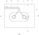
Fig. 1 is a schematic diagram of a structure of a printed circuit board according to an embodiment of the present disclosure; -
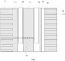
Fig. 2 is a cross-sectional view of the printed circuit board shown inFig. 1 ; -
Fig. 3 is a schematic diagram of a structure of a printed circuit board according to an embodiment of the present disclosure; -
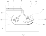
Fig. 4 is a schematic diagram of a structure of a printed circuit board according to an embodiment of the present disclosure; -
Fig. 5 is a schematic diagram of a structure of a printed circuit board according to an embodiment of the present disclosure; -
Fig. 6 is a schematic diagram of a structure of a printed circuit board according to an embodiment of the present disclosure; -
Fig. 7 is a schematic diagram of a structure of a printed circuit board according to an embodiment of the present disclosure; -
Fig. 8 is a cross-sectional view of the printed circuit board shown inFig. 7 ; -
Fig. 9 is a schematic diagram of a structure of a printed circuit board according to an embodiment of the present disclosure; -
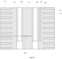
Fig. 10 is a cross-sectional view of the printed circuit board shown inFig. 9 ; -
Fig. 11 is a mode conversion diagram for a control group and a printed circuit board according to an embodiment of the present disclosure; and -
Fig. 12 is an impedance diagram for a control group and a printed circuit board according to an embodiment of the present disclosure. - Descriptions of reference numerals:
10-board body; 11-reference structure; 12-dielectric medium; 20-first differential via; 30-second differential via; 40-non-metallized hole; 41-first non-metallized hole; 42-second non-metallized hole; 50-differential line pair; 51-first differential line; and 52-second differential line. - The technical solutions in the embodiments of the present disclosure will be clearly and completely described below with reference to the accompanying drawings in the embodiments of the present disclosure, and it is apparent that the described embodiments are a part rather than all of the embodiments of the present disclosure. Based on the embodiments of the present disclosure, all other embodiments obtained by those of ordinary skill in art without creative work shall fall within the scope of protection of the present disclosure.
- In the description of the present disclosure, it should be understood that orientation or position relationships indicated by the terms such as "center", "longitudinal", "transverse", "length", "width", "thickness", "upper", "lower", "front", "back", "left", "right", "vertical", "horizontal", "top", "bottom", "inside", "outside", "clockwise", and "anticlockwise", are based on orientation or position relationships shown in the accompanying drawings, and are intended to facilitate the description of the present disclosure and simplify the description only, rather than indicate or imply that an apparatus or element referred needs to have a particular orientation or be constructed and operated in a particular orientation. Therefore, such terms should not be construed as limiting the present disclosure. Additionally, the terms "first" and "second" are used merely for the purpose of description, and should not be construed as indicating or implying relative importance or implying a quantity of indicated technical features. Therefore, features defined as "first" and "second" may explicitly or implicitly include one or more of the features. In the descriptions of the present disclosure, unless otherwise explicitly limited, "a plurality of" means two or more than two.
- It should also be understood that the terms used in the specification of the present disclosure are merely for the purpose of describing the specific embodiments and are not intended to limit the present disclosure. As used in the specification of the present disclosure and the appended claims, unless the context clearly indicates otherwise, the singular forms "a", "an", and "the" are intended to include the plural forms.
- It should be further understood that the term "and/or" used in the specification and the appended claims of the present disclosure refers to one of or any combination of more of associated listed items and all possible combinations thereof, and these combinations are included.
- A printed circuit board (PCB) serves as a primary carrier for signal transmission in a communication device product. During signal transmission, a via structure is a common structure causing impedance discontinuity in a link. Due to the robustness and strong anti-interference capability of differential signals, differential vias are basically used for signal transmission in a high-speed system.
- In the system link, a differential pair includes a differential via pair, a first transmission line, and a second transmission line. The differential via pair includes a differential via P and a differential via N. The first transmission line is connected with the differential via P, and the second transmission line is connected with the differential via N. Due to the layout of a chip, a connector, and other components, as well as a line-out method of a component pin, routing lengths of the first transmission line and the second transmission line are not consistent, leading to the existence of a propagation delay skew. A calculation formula of the differential pair skew is

- On the other hand, components such as a high-speed connector, a ball grid array (BGA) package, and a high-speed layer-changing via in the high-speed system are basically differential vias. A calculation formula for impedance of the differential via is as follows:

- In the above formula, Z denotes impedance of the differential via, S denotes a first spacing, d denotes a diameter of the differential via (i.e., a hole diameter of the differential via), and ε denotes a dielectric constant of the PCB. According to the calculation formula for the impedance of the differential via, it can be seen that the impedance may be increased by reducing the hole diameter of the differential via, upgrading the board, and increasing a distance between the differential via and a reference medium. However, taking a connector signal hole as an example, a via size cannot be changed for proper crimping. Additionally, upgrading a board grade will significantly increase product costs, and an excessive distance between the signal hole and the reference medium may cause some high-speed lines to lose reference, introducing additional crosstalk.
- In view of this, an embodiment of the present disclosure provides a printed circuit board, an electronic device, and a method for controlling a propagation delay skew of a differential pair, to reduce the propagation delay skew of differential signals.
- Referring to
Fig. 1 andFig. 2 , an embodiment of the present disclosure provides a printed circuit board, including aboard body 10. Theboard body 10 is provided with a first differential via 20, a second differential via 30, and at least onenon-metallized hole 40. The first differential via 20 and the second differential via 30 form a differential via pair. The at least onenon-metallized hole 40 is arranged around a periphery of the first differential via 20 and/or a periphery of the second differential via 30. Thenon-metallized holes 40 around the periphery of the first differential via 20 and thenon-metallized holes 40 around the periphery of the second differential via 30 are asymmetrically arranged. - According to the printed circuit board in the above embodiment, the
non-metallized holes 40 are arranged around the periphery of the differential via pair, and thenon-metallized holes 40 around the periphery of the first differential via 20 and thenon-metallized holes 40 around the periphery of the second differential via 30 are asymmetrically arranged, to reduce an effective dielectric constant of media around the peripheries of the corresponding differential vias, thereby adjusting the propagation delay skew of the differential signals of the differential vias, and then reducing the propagation delay skew of the differential signals of the differential pair; and by adjusting the impedance of the differential vias, impedance continuity of the differential pair is improved, and the transmission quality of the differential signals is improved. Additionally, the printed circuit board in this embodiment is simple in structure, easy to machine, high in operability, small in occupied space, and beneficial for high-density and high-speed routing. - It should be understood that the periphery of the differential via refers to an area surrounding the differential via, with a preset distance from the periphery of the differential via to a via wall of the differential via. The preset distance is designed according to actual requirements. This embodiment does not limit a specific value of the preset distance.
- Referring to
Fig. 1 , exemplarily, the differential pair includes the first differential via 20, a firstdifferential line 51, the second differential via 30, and a seconddifferential line 52. The firstdifferential line 51 and the first differential via 20 are connected. The seconddifferential line 51 and the second differential via 30 are connected. - It should be understood that the differential signal in the differential pair refers to a signal transmitted on the differential pair.
- Exemplarily, the
non-metallized hole 40 and the first differential via 20 are not interconnected. Thenon-metallized hole 40 and the second differential via 30 are not interconnected. - It should be understood that relative dielectric constants of the medium around the periphery of the first differential via 20 and the medium around the periphery of the second differential via 30 are greater than a relative dielectric constant of the
non-metalized holes 40, and therefore thenon-metallized holes 40 arranged around the periphery of the first differential via 20 and/or the periphery of the second differential via 30 can reduce the effective dielectric constant of the medium around the peripheries/periphery of the first differential via 20 and/or the second differential via 30.It should be understood that a metallized hole is formed in the medium to form the first differential via 20 or the second differential via 30. The medium is, for example, a dielectric medium 12 described below. - Exemplarily, a spacing distance between the
non-metallized holes 40 around the periphery of the first differential via 20 and the first differential via 20 is a first spacing. A spacing distance between thenon-metallized holes 40 around the periphery of the second differential via 20 and the second differential via 20 is a second spacing. When a routing length of the firstdifferential line 51 is greater than a routing length of the seconddifferential line 52, according to the above calculation formula for the skew of the differential pair, a first preset method is used to reduce the effective dielectric constant of the medium around the periphery of the first differential via 20; or, the first preset method is used to reduce the effective dielectric constant of the media around the peripheries of the first differential via 20 and the second differential via 30, and a reduction range of the effective dielectric constant of the medium around the periphery of the first differential via 20 is greater than a reduction range of the effective dielectric constant of the medium around the periphery of the second differential via 30.Therefore, the propagation delay skew of the differential signal of the first differential via 20 can be adjusted, thereby reducing the propagation delay skew of the differential signal of the differential pair. The first preset method includes at least one of the following: the number of thenon-metallized holes 40 around the periphery of the first differential via 20 is greater than the number of thenon-metallized holes 40 around the periphery of the second differential via 30; a radius of thenon-metallized holes 40 around the periphery of the first differential via 20 is greater than a radius of thenon-metallized holes 40 around the periphery of the second differential via 30; and the first spacing is smaller than the second spacing. - Exemplarily, when the routing length of the first
differential line 51 is less than the routing length of the seconddifferential line 52, according to the above calculation formula for the skew of the differential pair, a second preset method is used to reduce the effective dielectric constant of the medium around the periphery of the second differential via 20; or, the second preset method is used to reduce the effective dielectric constant of the media around the peripheries of the first differential via 20 and the second differential via 30, and the reduction range of the effective dielectric constant of the medium around the periphery of the first differential via 20 is less than the reduction range of the effective dielectric constant of the medium around the periphery of the second differential via 30.Therefore, the propagation delay skew of the differential signal of the second differential via 30 can be adjusted, thereby reducing the propagation delay skew of the differential signal of the differential pair. The second preset method includes at least one of the following: the number of thenon-metallized holes 40 around the periphery of the first differential via 20 is smaller than the number of thenon-metallized holes 40 around the periphery of the second differential via 30; the radius of thenon-metallized holes 40 around the periphery of the first differential via 20 is smaller than the radius of thenon-metallized holes 40 around the periphery of the second differential via 30; and the first spacing is greater than the second spacing. - Referring to
Fig. 1 andFig. 2 , in some embodiments, theboard body 10 includesreference structures 11 and the dielectric medium 12.Thedielectric medium 12 is filled between thereference structures 11, the first differential via 20, and the second differential via 30.Thenon-metallized hole 40 is arranged in thedielectric medium 12. Alternatively, thenon-metallized hole 40 is arranged in thedielectric medium 12 and thereference structures 11. - Exemplarily, a plurality of
reference structures 11 are included. A space between theadjacent reference structures 11 is filled with thedielectric medium 12. - Exemplarily, the relative dielectric constant of the dielectric medium 12 ranges from 2.9 to 4.5, such as 2.9, 3.0, 3.5, 4.0, 4.5, and any other suitable value within the range of 2.9 to 4.5.It should be understood that the
non-metallized hole 40 is filled with air and has the relative dielectric constant of 1, and therefore combined use of thedielectric medium 12 and thenon-metallized hole 40 can reduce the effective dielectric constant of the corresponding differential via reference structure, thereby increasing a signal transmission speed of the differential via, adjusting the problem about the inconsistent signal transmission speed of the differential pair, and reducing the propagation delay skew of the differential signals of the differential pair. - Exemplarily, both the first differential via 20 and the second differential via 30 are metallized holes.
- Exemplarily, the differential via pair is provided with a pair of differential lines, namely a
differential line pair 50. Thedifferential line pair 50 includes the firstdifferential line 51 and the second differential line 52.A line-outlet position of the first differential via 20 is connected with the first differential line 51.A line-outlet position of the second differential via 30 is connected with the seconddifferential line 52. - Referring to
Fig. 1 , exemplarily, the firstdifferential line 51 and the seconddifferential line 52 are differential lines of unequal lengths, with a propagation delay skew between them. By asymmetrically arranging thenon-metallized holes 40 around the periphery of the first differential via 20 and thenon-metallized holes 40 around the periphery of the second differential via 30, the propagation delay skew of the differential signals in the differential pair can be reduced. - Exemplarily, a via wall surface of the
non-metallized hole 40 is not plated, and the via is not plugged. Thenon-metallized hole 40 is completely filled with air. - The number of
non-metallized holes 40 may be designed according to actual requirements. Exemplarily, the number of thenon-metallized holes 40 is one or more, such as one, two, three, four, five, six, or more. Exemplarily, referring toFig. 1 andFig. 2 , onenon-metallized hole 40 is provided, and is arranged around the periphery of the first differential via 20 or the second differential via 30. Referring toFig.3 to Fig. 6 , exemplarily, a plurality ofnon-metallized holes 40 are included. - The radius and the position of the
non-metallized hole 40, as well as a spacing L1 (please refer toFig.1 ) between thenon-metallized hole 40 and the corresponding differential via, may all be designed according to simulation, manufacturer processing capabilities, etc. Referring toFig.3 to Fig. 6 , exemplarily, a plurality ofnon-metallized holes 40 are included, and the radii of thenon-metallized holes 40 may be all the same, partially the same, partially different, or completely different. The spacing L1 between eachnon-metallized hole 40 and the corresponding differential via may be the same, partially the same, partially different, or completely different. It should be understood that the smaller the spacing L1 between thenon-metallized hole 40 and the corresponding differential via, and the larger the radius of thenon-metallized hole 40, the faster the differential signal transmission speed of the differential via corresponding to thenon-metallized hole 40. - Exemplarily, at least three
non-metallized holes 40 are included. A spacing between the adjacentnon-metallized holes 40 is L2, and each L2 may be completely the same, partially the same, or completely different. - It should be understood that at least one
non-metallized hole 40 is arranged around the periphery of the first differential via 20 and/or the periphery of the second differential via 30. The asymmetric arrangement of the non-metallized holes 40 around the peripheries of the first differential via 20 and the second differential via 30 includes at least one of the following: the number of the non-metallized holes 40 around the periphery of the first differential via 20 is different from the number of the non-metallized holes 40 around the periphery of the second differential via 30; the radius of the non-metallized holes 40 around the periphery of the first differential via 20 is different from the radius of the non-metallized holes 40 around the periphery of the second differential via 30; and the positions of the non-metallized holes 40 around the periphery of the first differential via 20 are asymmetrically located relative to the positions of the non-metallized holes 40 around the periphery of the second differential via 30.Exemplarily, the number of the non-metallized holes 40 around the periphery of the first differential via 20 is different from the number of the non-metallized holes 40 around the periphery of the second differential via 30, including: arranging the non-metallized holes 40 only around the periphery one of the first differential via 20 and/or the second differential via 30; or, arranging the non-metallized holes 40 around the peripheries of both the first differential via 20 and the second differential via 30, and the non-metallized holes 40 around the periphery of the first differential via 20 and the non-metallized holes 40 around the periphery of the second differential via 30 being asymmetrically arranged. - Referring to
Fig. 1 to Fig. 3 , andFig. 5 , in some embodiments, at least onenon-metallized hole 40 is arranged around the periphery of the first differential via 20 or the second differential via 30. Exemplarily, the number of thenon-metallized holes 40 arranged around the periphery of one of the first differential via 20 and the second differential via 30 is zero, and allnon-metallized holes 40 are arranged around the periphery of the other one of the first differential via 20 and the second differential via 30, thereby achieving the asymmetric arrangement of thenon-metallized holes 40 around the periphery of the first differential via 20 and thenon-metallized holes 40 around the periphery of the second differential via 30. - Referring to
Fig. 4 andFig. 6 , in some embodiments, a part of the at least onenon-metallized hole 40 is arranged around the periphery of the first differential via 20, and the other part of the at least onenon-metallized hole 40 is arranged around the periphery of the second differential via 30. Thenon-metallized holes 40 around the periphery of the first differential via 20 and thenon-metallized holes 40 around the periphery of the second differential via 30 are asymmetrically arranged. - Referring to
Fig. 4 andFig. 6 , in some implementations, the at least onenon-metallized hole 40 includes at least one firstnon-metallized hole 41 and at least one secondnon-metallized hole 42. The at least one firstnon-metallized hole 41 is arranged around the periphery of the first differential via 20.The at least one secondnon-metallized hole 42 is arranged around the periphery of the second differential via 30.The at least one firstnon-metallized hole 41 and the at least one secondnon-metallized hole 42 are asymmetrically arranged. Therefore, the asymmetric arrangement of thenon-metallized holes 40 around the periphery of the first differential via 20 and thenon-metallized holes 40 around the periphery of the second differential via 30 can be achieved. - It should be understood that the number of the first
non-metallized holes 41 and the secondnon-metallized holes 42 may be designed according to actual requirements, such as one, two, three, or more. - Referring to
Fig.4 andFig. 6 , in some implementations, a plurality of firstnon-metallized holes 41 are included. The plurality of firstnon-metallized holes 41 are arranged around the periphery of the first differential via 20 at intervals in a circumferential direction of the first differential via 20. - Referring to
Fig. 4 andFig. 6 , in some implementations, the number of thenon-metallized holes 40 around the periphery of the first differential via 20 is different from the number of thenon-metallized holes 40 around the periphery of the second differential via 30, thereby achieving the asymmetric arrangement of thenon-metallized holes 40 around the periphery of the first differential via 20 and thenon-metallized holes 40 around the periphery of the second differential via 30.Exemplarily,the number of thenon-metallized holes 40 around the periphery of the first differential via 20 is greater than the number of thenon-metallized holes 40 around the periphery of the second differential via 30.Exemplarily, the number of thenon-metallized holes 40 around the periphery of the first differential via 20 is less than the number of thenon-metallized holes 40 around the periphery of the second differential via 30. - In some implementations, the radius of the
non-metallized holes 40 around the periphery of the first differential via 20 is different from the radius of thenon-metallized holes 40 around the periphery of the second differential via 30, thereby achieving the asymmetric arrangement of thenon-metallized holes 40 around the periphery of the first differential via 20 and thenon-metallized holes 40 around the periphery of the second differential via 30. Exemplarily, the radius of at least one of the at least one firstnon-metallized hole 41 is different from the radius of at least one of the at least one secondnon-metallized hole 42. - In some implementations, the position of at least one
non-metallized hole 40 around the periphery of the first differential via 20 is asymmetrical to the position of at least onenon-metallized hole 40 around the periphery of the second differential via 30, thereby achieving the asymmetric arrangement of thenon-metallized holes 40 around the periphery of the first differential via 20 and thenon-metallized holes 40 around the periphery of the second differential via 30. - Exemplarily, the number of the
non-metallized holes 40 around the periphery of the first differential via 20 is the same as the number of thenon-metallized holes 40 around the periphery of the second differential via 30, and the position of at least onenon-metallized hole 40 around the periphery of the first differential via 20 is asymmetrical to the position of at least onenon-metallized hole 40 around the periphery of the second differential via 30. - Referring to
Fig. 4 andFig. 6 , exemplarily, the number of thenon-metallized holes 40 around the periphery of the first differential via 20 is greater than the number of thenon-metallized holes 40 around the periphery of the second differential via 30, and the positions of the secondnon-metallized holes 42 around the periphery of the second differential via 30 are symmetrical to the positions of some of the firstnon-metallized holes 41 around the periphery of the first differential via 20. - Exemplarily, the number of the
non-metallized holes 40 around the periphery of the first differential via 20 is greater than the number of thenon-metallized holes 40 around the periphery of the second differential via 30, and the positions of the secondnon-metallized holes 42 around the periphery of the second differential via 30 are asymmetrical to the position of any one of the firstnon-metallized holes 41 around the periphery of the first differential via 20. - In some implementations, a minimum distance (e.g., L1 in
Fig. 1 ) between a via wall of the first differential via 20 or a via wall of the second differential via 30 and a hole wall of thenon-metallized hole 40 is 2 mil to 20 mil, such as 2 mil, 4 mil, 8 mil, 10 mil, 15 mil, 20 mil, and any other suitable value between 2 mil and 15 mil. Exemplarily, the minimum distance L1 between the via wall of the first differential via 20 and a hole wall of the firstnon-metallized hole 41 is 2 mil to 20 mil. Exemplarily, the minimum distance between the via wall of the second differential via 30 and a via wall of the secondnon-metallized hole 42 is 2 mil to 20 mil. - Referring to
Fig.1 ,Fig. 3 , andFig. 5 , in some embodiments, thenon-metallized hole 40 includes at least one of a circular hole, a kidney-shaped hole, a square hole, an arc hole, an oval hole, etc. Exemplarily, when thenon-metallized hole 40 is a non-circular hole, the radius of thenon-metallized hole 40 is equal to half of a width of thenon-metallized hole 40. - Referring to
Fig. 2 , andFig. 7 toFig. 10 , in some embodiments, thenon-metallized hole 40 includes a non-metallized through hole, a non-metallized blind hole, or a non-metallized buried hole. Exemplarily, considering the routing density in the printed circuit board and no damage to the integrity of a power plane, thenon-metallized hole 40 includes the non-metallized blind hole or the non-metallized buried hole, and a depth of thenon-metallized hole 40 may be set according to actual requirements. - The performance of a printed circuit board without non-metallized holes 40 (a control group, S0) and the performance of the printed circuit board (S1) in this embodiment of the present disclosure are compared below.
- Referring to
Fig. 11, Fig. 11 is a mode conversion diagram for the control group and the printed circuit board according to this embodiment of the present disclosure. InFig. 11 , a horizontal axis represents a signal frequency, and a vertical axis represents a signal amplitude.As can be seen fromFig. 11 , a skew (a propagation delay skew) value of a differential signal of a differential pair in the control group is 2.06 ps, while a skew value of the differential signal of the differential pair in the printed circuit board of this embodiment is 0.06 ps.lt can be inferred that according to the printed circuit board in this embodiment, by arranging the at least onenon-metallized hole 40 around the periphery of the first differential via 20 and/or the periphery of the second differential via 30 and asymmetrically arranging thenon-metallized holes 40 around the periphery of the first differential via 20 and thenon-metallized holes 40 around the periphery of the second differential via 30, the signal transmission speed of the differential vias can be increased, the skew value of the differential signals is reduced or improved, the signal transmission quality is improved, and the routing space is increased. - Referring to
Fig. 12, Fig. 12 is an impedance diagram for a control group and the printed circuit board according to this embodiment of the present disclosure. InFig. 12 , a horizontal axis represents propagation time, and a vertical axis represents impedance of a differential pair. As can be seen fromFig. 12 , according to the printed circuit board in this embodiment, by arranging the at least onenon-metallized hole 40 around the periphery of the first differential via 20 and/or the periphery of the second differential via 30 and asymmetrically arranging thenon-metallized holes 40 around the periphery of the first differential via 20 and thenon-metallized holes 40 around the periphery of the second differential via 30, the impedance can be increased, the impedance continuity of a system link is improved, insertion loss fluctuations are reduced, and signal reflections are reduced. - An embodiment of the present disclosure further provides an electronic device, including the printed circuit board according to any one of the above embodiments.
- An embodiment of the present disclosure further provides a method for controlling a propagation delay skew of a differential pair on a printed circuit board, including:
arranging at least onenon-metallized hole 40 around a periphery of a first differential via 20 and/or a periphery of a second differential via 30, where the first differential via 20 and the second differential via 30 form a differential via pair, and thenon-metallized holes 40 around the periphery of the first differential via 20 and thenon-metallized holes 40 around the periphery of the second differential via 30 are asymmetrically arranged. - According to the method for controlling a propagation delay skew of a differential pair on a printed circuit board in the above embodiment, by arranging the
non-metallized holes 40 around the periphery of the first differential via 20 and/or the periphery of the second differential via 30, and asymmetrically arranging thenon-metallized holes 40 around the periphery of the first differential via 20 and thenon-metallized holes 40 around the periphery of the second differential via 30, an effective dielectric constant of media around the peripheries of the corresponding differential vias is reduced, thereby adjusting the propagation delay skew of differential signals of the differential vias, and then reducing the propagation delay skew of the differential signals of the differential pair; and by adjusting the impedance of the differential vias, impedance continuity of the differential pair is improved, and the transmission quality of the differential signals is improved. - Exemplarily, the printed circuit board includes the printed circuit board according to any one of the above embodiments.
- The printed circuit board and the method for controlling a propagation delay skew of a differential pair on a printed circuit board in the above embodiments may be applied to a multi-layer printed circuit board structure designed with BGA differential vias, high-speed connector crimp vias, high-speed layer-changing differential vias, etc., and is particularly suitable for a printed circuit board structure in a high-speed backpanel system with a rate of 112 Gbps or above.
- It should be understood that the common practice for fan-out differential lines from the BGA differential vias is to adjust the equal length at via positions. As a signal rate increases, a pitch spacing of BGA differential signal holes may decrease to 0.6 mm, making it impossible to adjust fan-out lines from the differential vias to achieve the equal length for the fan-out differential lines from the BGA vias. Therefore, the differential lines need to be internally adjusted to be equal in length outside the BGA, which introduces additional impedance discontinuous points. Therefore, the skew of the differential vias may be adjusted and the impedance discontinuous points may be reduced by arranging a certain number of
non-metallized holes 40 around a periphery of a via with a longer trace in a BGA fan-out differential pair. A drilling diameter and the number of thenon-metallized holes 40 may be obtained through simulation, and placement positions need to satisfy manufacturability. - It should be understood that the skew of the system link may be adjusted through crimp via positions of a connector in a channel. Since the connector crimp vias are relatively far from surrounding signal holes or grounding shield holes, a larger number of
non-metallized holes 40 with larger diameters/slot widths may be placed to adjust the problem of inconsistent transmission speeds in the differential pair. Additionally, the drilling diameters of differential vias for the connector on the printed circuit board mostly range from 0.32 mm to 0.6 mm, and the hole diameters are relatively large, causing that the impedance of the differential vias is significantly lower than that of the system link. Moreover, the differential vias for the connector on the printed circuit board are the crimp holes required to mate with the connector for crimping, and therefore, modification cannot be achieved. By arranging thenon-metallized holes 40 around the differential via pair, the impedance of the differential vias can be increased to some extent while improving the skew, thereby enhancing the impedance continuity of the link. - It should be understood that the high-speed layer-changing differential vias are applied to a scenario where a high-speed link needs replacement of a routing layer, which are common in the printed circuit board. Similar to an application scenario of BGA fan-out differential vias, the
non-metallized holes 40 may be arranged around one of signal holes of the high-speed layer-changing vias to adjust the skew value of a high-speed differential signal and reduce the discontinuous points in the system link. Typically, only return ground vias are arranged around the high-speed layer-changing differential vias, allowing for the placement of morenon-metallized holes 40 with larger diameters. However, the routing of nearby high-speed signals cannot be interfered. - In the description of the embodiments of the present disclosure, it should be noted that, unless otherwise explicitly specified and limited, the terms "mounted", "connected", "linked", "mechanically coupled", and "coupled" are to be understood in a broad sense. For example, a connection may be a fixed connection, a detachable connection, or an integral connection. Alternatively, the connection may be a mechanical connection or an electrical connection. Alternatively, the connection may be a direct connection, an indirect connection through an intermediary, or internal communication between two elements, or an interaction relationship between two elements. Mechanical coupling or coupling between two components includes direct coupling and indirect coupling, such as a direct fixed connection and a connection through a transmission mechanism. Those of ordinary skill in the art may understand the specific meanings of the foregoing terms in the present disclosure according to specific situations.
- In the embodiments of the present disclosure, unless otherwise expressly specified and limited, a first feature being "above" or "below" a second feature may include direct contact of the first feature and the second feature, or may also include indirect contact of the first feature and the second feature through an additional feature therebetween. In addition, the first feature being "over", "above", and "on" the second feature includes the first feature being over and above the second feature, or merely indicates that a level of the first feature is higher than that of the second feature.The first feature being "under", "below", and "underneath" the second feature includes the first feature being under and below the second feature, or merely indicates that the level of the first feature is lower than that of the second feature.
- The above disclosure provides many different implementations or examples for implementing different structures of the present disclosure. To simplify the present disclosure, components and settings in particular examples are described above. Certainly, they are merely examples and are not intended to limit the present disclosure. Further, the embodiments of the present disclosure may reuse reference numerals and/or reference letters across different examples for simplicity and clarity, which does not indicate any relationship between the various implementations and/or settings discussed. Moreover, the embodiments of the present disclosure provide examples of various particular processes and materials, but those of ordinary skill in the art may be aware of applicability of another process and/or use of another material.
- In the descriptions of this specification, descriptions using reference terms "an implementation", "some implementations", "an exemplary implementation", "an example", "a specific example", or "some examples" mean that specific method steps, features, structures, materials, or characteristics described with reference to the implementations or examples are included in at least one implementation or example of the present disclosure. In this specification, illustrative expressions of the above terms do not necessarily refer to the same implementation or example. Moreover, the described specific method steps, features, structures, materials, or characteristics may be combined in a suitable manner in any one or more of the implementations or examples.
- The above contents are merely specific implementations of the present disclosure, but the scope of protection of the present disclosure is not limited thereto; and any technical personnel familiar with the technical field may easily think of various equivalent modifications or substitutions within the technical scope disclosed by the embodiments of the present disclosure, and these modifications or substitutions shall be included within the scope of protection of the present disclosure. Therefore, the scope of protection of the present disclosure should be based on the scope of protection of the claims.
Claims (10)
- A printed circuit board, comprising a board body, the board body being provided with a first differential via, a second differential via, and at least one non-metallized hole, and the first differential via and the second differential via forming a differential via pair;
wherein the at least one non-metallized hole is arranged around a periphery of the first differential via and/or a periphery of the second differential via, and the non-metallized holes around the periphery of the first differential via and the non-metallized holes around the periphery of the second differential via are asymmetrically arranged. - The printed circuit board according to claim 1, wherein the at least one non-metallized hole is arranged around the periphery of the first differential via or the periphery of the second differential via.
- The printed circuit board according to claim 1, wherein the at least one non-metallized hole comprises:at least one first non-metallized hole arranged around the periphery of the first differential via; andat least one second non-metallized hole, arranged around the periphery of the second differential via, and the at least one first non-metallized hole and the at least one second non-metallized hole are asymmetrically arranged.
- The printed circuit board according to claim 3, wherein a plurality of first non-metallized holes are comprised and arranged around the periphery of the first differential via at intervals in a circumferential direction of the first differential via.
- The printed circuit board according to claim 3, wherein the number of the non-metallized holes around the periphery of the first differential via is different from the number of the non-metallized holes around the periphery of the second differential via; and/or,
a radius of the non-metallized holes around the periphery of the first differential via is different from a radius of the non-metallized holes around the periphery of the second differential via. - The printed circuit board according to claim 3, wherein positions of at least one non-metallized hole around the periphery of the first differential via are asymmetrical to positions of at least one non-metallized hole around the periphery of the second differential via.
- The printed circuit board according to claim 1, wherein the non-metallized hole comprises at least one of a circular hole, a kidney-shaped hole, a square hole, an arc hole, and an oval hole.
- The printed circuit board according to any one of claims 1 to 7, wherein the board body comprises:a reference structure; anda dielectric medium, filled between the reference structure, the first differential via, and the second differential via; and the non-metallized hole is arranged on the dielectric medium, or the non-metallized hole is arranged on the dielectric medium and the reference structure.
- An electronic device, comprising the printed circuit board according to any one of claims 1 to 8.
- A method for controlling a propagation delay skew of a differential pair on a printed circuit board, comprising:
arranging at least one non-metallized hole around a periphery of a first differential via and/or a periphery of a second differential via, the first differential via and the second differential via forming a differential via pair, and the non-metallized holes around the periphery of the first differential via and the non-metallized holes around the periphery of the second differential via being asymmetrically arranged.
Applications Claiming Priority (2)
| Application Number | Priority Date | Filing Date | Title |
|---|---|---|---|
| CN202211058162.1A CN117440594A (en) | 2022-08-30 | 2022-08-30 | Printed circuit board, electronic device, and method of controlling propagation delay difference of differential pair |
| PCT/CN2023/102207 WO2024045803A1 (en) | 2022-08-30 | 2023-06-25 | Printed circuit board, electronic device, and method for controlling propagation delay skew of differential pair |
Publications (2)
| Publication Number | Publication Date |
|---|---|
| EP4583639A1 true EP4583639A1 (en) | 2025-07-09 |
| EP4583639A4 EP4583639A4 (en) | 2025-12-17 |
Family
ID=89557143
Family Applications (1)
| Application Number | Title | Priority Date | Filing Date |
|---|---|---|---|
| EP23858842.0A Pending EP4583639A4 (en) | 2022-08-30 | 2023-06-25 | Circuit board, electronic device and method for controlling the runtime delay shift of a differential pair |
Country Status (3)
| Country | Link |
|---|---|
| EP (1) | EP4583639A4 (en) |
| CN (1) | CN117440594A (en) |
| WO (1) | WO2024045803A1 (en) |
Family Cites Families (11)
| Publication number | Priority date | Publication date | Assignee | Title |
|---|---|---|---|---|
| US6503103B1 (en) * | 1997-02-07 | 2003-01-07 | Teradyne, Inc. | Differential signal electrical connectors |
| CN1799290A (en) * | 2003-06-02 | 2006-07-05 | 日本电气株式会社 | Compact via transmission line for printed circuit board and its designing method |
| CN100574552C (en) * | 2005-08-12 | 2009-12-23 | 鸿富锦精密工业(深圳)有限公司 | Printed circuit board (PCB) |
| CN102291929A (en) * | 2011-06-24 | 2011-12-21 | 福建星网锐捷网络有限公司 | Printed circuit board and method for controlling impedance of through hole structure on same |
| CN108336593B (en) * | 2012-06-29 | 2019-12-17 | 安费诺有限公司 | Low-cost high-performance radio frequency connector |
| CN203896579U (en) * | 2014-03-31 | 2014-10-22 | 深圳市兴森快捷电路科技股份有限公司 | Difference line structure for optimizing impedance |
| CN107155258B (en) * | 2017-04-25 | 2019-05-10 | 安徽宏鑫电子科技有限公司 | A kind of asymmetry via hole printed circuit board |
| CN109379832A (en) * | 2018-09-19 | 2019-02-22 | 中国电子科技集团公司第五十二研究所 | A Differential Line Compensation Method for Improving the Anti-interference Ability of Differential Signals |
| CN110536548A (en) * | 2019-09-20 | 2019-12-03 | 苏州浪潮智能科技有限公司 | A printed circuit board and electronic product |
| US11343905B2 (en) * | 2020-02-28 | 2022-05-24 | Hewlett Packard Enterprise Development Lp | Asymmetric differential via stubs for skew compensation |
| CN114143961B (en) * | 2021-11-29 | 2023-07-21 | 中汽创智科技有限公司 | Circuit board |
-
2022
- 2022-08-30 CN CN202211058162.1A patent/CN117440594A/en active Pending
-
2023
- 2023-06-25 WO PCT/CN2023/102207 patent/WO2024045803A1/en not_active Ceased
- 2023-06-25 EP EP23858842.0A patent/EP4583639A4/en active Pending
Also Published As
| Publication number | Publication date |
|---|---|
| CN117440594A (en) | 2024-01-23 |
| WO2024045803A1 (en) | 2024-03-07 |
| EP4583639A4 (en) | 2025-12-17 |
Similar Documents
| Publication | Publication Date | Title |
|---|---|---|
| US6372996B2 (en) | Circuit board having shielding planes with varied void opening patterns for controlling the impedance and the transmission time | |
| US6388208B1 (en) | Multi-connection via with electrically isolated segments | |
| US9137887B2 (en) | Via structure for transmitting differential signals | |
| US7448909B2 (en) | Preferential via exit structures with triad configuration for printed circuit boards | |
| US8440910B2 (en) | Differential signal transmission cable | |
| US20170181270A1 (en) | Circuit board via configurations for high frequency signaling | |
| US8049118B2 (en) | Printed circuit board | |
| US20050201065A1 (en) | Preferential ground and via exit structures for printed circuit boards | |
| US9554455B2 (en) | Method and apparatus for reducing far-end crosstalk in electrical connectors | |
| US6225568B1 (en) | Circuit board having shielding planes with varied void opening patterns for controlling the impedance and the transmission time | |
| JP2000507427A (en) | Bidirectional, non-solid, impedance-controlled reference plane | |
| CN203840633U (en) | Flexible circuit board and signal transmission device | |
| JP5320704B2 (en) | Multilayer printed circuit board, connection structure between multilayer printed circuit board and coaxial connector | |
| EP4583639A1 (en) | Printed circuit board, electronic device, and method for controlling propagation delay skew of differential pair | |
| CN117177435A (en) | Circuit board connector package | |
| CN110784995A (en) | Circuit board structure | |
| WO2025227983A1 (en) | Differential via hole structure, ball grid array assembly, printed circuit board, and communication device | |
| US7196906B1 (en) | Circuit board having segments with different signal speed characteristics | |
| CN220653612U (en) | Circuit board and electronic equipment | |
| US20240276634A1 (en) | Shielding structure and circuit board | |
| CN210328147U (en) | Millimeter wave active antenna unit and interconnection structure between PCB boards | |
| WO2025232394A1 (en) | Via structure of circuit board, circuit board and electronic device | |
| US20260032807A1 (en) | Pin arrangement structure, package substrate, and package structure | |
| US20250280493A1 (en) | Vertical conductive structure transition impedance optimization | |
| US12526912B2 (en) | Carrier structure |
Legal Events
| Date | Code | Title | Description |
|---|---|---|---|
| STAA | Information on the status of an ep patent application or granted ep patent |
Free format text: STATUS: THE INTERNATIONAL PUBLICATION HAS BEEN MADE |
|
| PUAI | Public reference made under article 153(3) epc to a published international application that has entered the european phase |
Free format text: ORIGINAL CODE: 0009012 |
|
| STAA | Information on the status of an ep patent application or granted ep patent |
Free format text: STATUS: REQUEST FOR EXAMINATION WAS MADE |
|
| 17P | Request for examination filed |
Effective date: 20250306 |
|
| AK | Designated contracting states |
Kind code of ref document: A1 Designated state(s): AL AT BE BG CH CY CZ DE DK EE ES FI FR GB GR HR HU IE IS IT LI LT LU LV MC ME MK MT NL NO PL PT RO RS SE SI SK SM TR |
|
| DAV | Request for validation of the european patent (deleted) | ||
| DAX | Request for extension of the european patent (deleted) | ||
| A4 | Supplementary search report drawn up and despatched |
Effective date: 20251118 |
|
| RIC1 | Information provided on ipc code assigned before grant |
Ipc: H05K 1/02 20060101AFI20251112BHEP Ipc: H05K 1/11 20060101ALI20251112BHEP |