EP4583404A1 - I2c interface circuit, corresponding electronic device and method of operation - Google Patents
I2c interface circuit, corresponding electronic device and method of operation Download PDFInfo
- Publication number
- EP4583404A1 EP4583404A1 EP24218805.0A EP24218805A EP4583404A1 EP 4583404 A1 EP4583404 A1 EP 4583404A1 EP 24218805 A EP24218805 A EP 24218805A EP 4583404 A1 EP4583404 A1 EP 4583404A1
- Authority
- EP
- European Patent Office
- Prior art keywords
- voltage
- pull
- value
- low
- threshold
- Prior art date
- Legal status (The legal status is an assumption and is not a legal conclusion. Google has not performed a legal analysis and makes no representation as to the accuracy of the status listed.)
- Granted
Links
Images

Classifications
-
- H—ELECTRICITY
- H03—ELECTRONIC CIRCUITRY
- H03K—PULSE TECHNIQUE
- H03K5/00—Manipulating of pulses not covered by one of the other main groups of this subclass
- H03K5/01—Shaping pulses
- H03K5/08—Shaping pulses by limiting; by thresholding; by slicing, i.e. combined limiting and thresholding
- H03K5/082—Shaping pulses by limiting; by thresholding; by slicing, i.e. combined limiting and thresholding with an adaptive threshold
-
- H—ELECTRICITY
- H03—ELECTRONIC CIRCUITRY
- H03K—PULSE TECHNIQUE
- H03K17/00—Electronic switching or gating, i.e. not by contact-making and –breaking
- H03K17/002—Switching arrangements with several input- or output terminals
- H03K17/005—Switching arrangements with several input- or output terminals with several inputs only
-
- G—PHYSICS
- G06—COMPUTING OR CALCULATING; COUNTING
- G06F—ELECTRIC DIGITAL DATA PROCESSING
- G06F13/00—Interconnection of, or transfer of information or other signals between, memories, input/output devices or central processing units
- G06F13/38—Information transfer, e.g. on bus
- G06F13/42—Bus transfer protocol, e.g. handshake; Synchronisation
- G06F13/4282—Bus transfer protocol, e.g. handshake; Synchronisation on a serial bus, e.g. I2C bus, SPI bus
-
- H—ELECTRICITY
- H03—ELECTRONIC CIRCUITRY
- H03K—PULSE TECHNIQUE
- H03K19/00—Logic circuits, i.e. having at least two inputs acting on one output; Inverting circuits
- H03K19/0175—Coupling arrangements; Interface arrangements
- H03K19/017581—Coupling arrangements; Interface arrangements programmable
-
- H—ELECTRICITY
- H03—ELECTRONIC CIRCUITRY
- H03K—PULSE TECHNIQUE
- H03K5/00—Manipulating of pulses not covered by one of the other main groups of this subclass
- H03K5/22—Circuits having more than one input and one output for comparing pulses or pulse trains with each other according to input signal characteristics, e.g. slope, integral
- H03K5/24—Circuits having more than one input and one output for comparing pulses or pulse trains with each other according to input signal characteristics, e.g. slope, integral the characteristic being amplitude
Definitions
- Switching converters with embedded I 2 C interface may be implemented, for instance, in class-D power amplifiers (audio amplifiers) used in car radio apparatuses.
- Switching devices such as class-D amplifiers and switching converters produce electronic noise that can propagate to the digital interfaces of the device itself and thus affect the proper operation of such interfaces.
- a digital interface that can be affected by noise is the I 2 C interface (see, as a reference, the User manual UM10204 by NXP, "I 2 C-bus specification and user manual", Rev. 7.0, 1 October 2021, available online at https://www.nxp.com/docs/en/user-guide/UM10204.pdf) .
- the input comparators of an I 2 C interface which are designed to discern between the high level and the low level of an input digital signal, are thus usually designed to have large hysteresis so as to be robust against noise (i.e., avoid spurious commutations due to noise).
- V pu a pin of the electronic device for receiving the external pull-up voltage V pu .
- the high threshold V IH and the low threshold V IL for the input comparators of the I 2 C interface can be generated within the device, and a wider range for hysteresis can be achieved.
- TAS2764 Digital Input Mono Class-D Audio Amplifier With Speaker IV Sense
- a drawback of the known solution discussed above is that a conductive trace has to be provided on the board (PCB) to route the pull-up voltage V pu to the electronic device, and a pin of the electronic device has to be used for receiving the external pull-up voltage V pu .
- the available pin count is limited and dedicating one pin to receiving the external pull-up voltage V pu is undesirable.
- One or more embodiments of the present disclosure contribute in providing improved I 2 C interface circuits.
- such an object can be achieved by an I 2 C interface circuit having the features set forth in the claims that follow.
- One or more embodiments may relate to a corresponding electronic device (e.g., a switching converter or switching power amplifier).
- a corresponding electronic device e.g., a switching converter or switching power amplifier.
- One or more embodiments may relate to a corresponding method of operation.
- an I 2 C interface circuit is operatable at a low pull-up voltage and at a high pull-up voltage.
- the I 2 C interface circuit includes a first pin configured to receive a clock signal and a second pin configured to receive a data signal.
- the I 2 C interface circuit includes a first comparator stage coupled to the first pin and configured to compare the received clock signal to a low threshold and a high threshold to produce an internal clock signal.
- the I 2 C interface circuit includes a second comparator stage coupled to the second pin and configured to compare the received data signal to the low threshold and the high threshold to produce an internal data signal.
- the first comparator stage and the second comparator stage are programmed by default to operate in a first operating mode.
- the low threshold is set to a first fractional value of the high pull-up voltage and the high threshold is set to a second fractional value of the low pull-up voltage (e.g., with the first fractional value lower than the second fractional value).
- the first comparator stage and the second comparator stage are switchable, upon reception via the I 2 C interface of a programming frame that conveys a current value of the pull-up voltage, to a second operating mode.
- the low threshold is set to the first fractional value of the current pull-up voltage and the high threshold is set to the second fractional value of the current pull-up voltage.
- One or more embodiments may thus provide an I 2 C interface circuit that is compatible with plural values of the pull-up voltage and is robust in terms of comparison hysteresis, without the need of routing the pull-up voltage to the interface itself.
- an electronic device includes an I 2 C interface circuit according to one or more embodiments, and a processing circuit.
- the processing circuit is configured to receive, via the I 2 C interface circuit, the programming frame that conveys the current value of the pull-up voltage, and switch the first comparator stage and the second comparator stage of the I 2 C interface circuit to the second operating mode as a function thereof.
- a method of operating an I 2 C interface circuit or an electronic device includes:
- references to "an embodiment” or “one embodiment” in the framework of the present description is intended to indicate that a particular configuration, structure, or characteristic described in relation to the embodiment is included in at least one embodiment.
- phrases such as “in an embodiment” or “in one embodiment” that may be present in one or more points of the present description do not necessarily refer to one and the same embodiment.
- particular configurations, structures, or characteristics may be combined in any adequate way in one or more embodiments.
- an I 2 C interface includes two (bidirectional) communication lines, in particular a serial data line (SDA) and a serial clock line (SCL) . Therefore, an I 2 C interface includes two I/O pins, each of which is connected to a respective comparator stage that is configured to discern between the high level and the low level of the respective input digital signal.
- SDA serial data line
- SCL serial clock line
- one or more embodiments relate to an I 2 C interface circuit where the input comparator stage(s) are programmable, via the I 2 C interface itself (i.e., without the need of resorting to additional I/O pins), so as to switch between:
- the comparator stages operate by default with small hysteresis and can operate at any one of the possible values V pu_low and V pu_high of the pull-up voltage (e.g., 1.8 V and 3.3 V) .
- V pu_low and V pu_high of the pull-up voltage e.g., 1.8 V and 3.3 V
- the I 2 C interface receives a frame indicating whether the actual pull-up voltage is equal to V pu_low (e.g., 1.8 V) or V pu_high (e.g., 3.3 V).
- V pu_low e.g., 1.8 V
- V pu_high e.g., 3.3 V
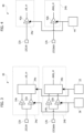
- FIG. 1 is a circuit block diagram exemplary of an I 2 C interface circuit 10 according to one or more embodiments of the present description.
- the I 2 C interface includes a first I/O pin 12a configured to receive a clock signal I2Cclk, and a second I/O pin 12b configured to receive a data signal I2Cdata.
- At least three comparators 14a, 16a and 18a are coupled to pin 12a to receive signal I2Cclk, and similarly at least three comparators 14b, 16b and 18b are coupled to pin 12b to receive signal I2Cdata.
- Comparators 14a and 14b are compatible with all the possible levels of the pull-up voltage (i.e., at least V pu_low and V pu_high ) that the I 2 C interface is expected to operate with (e.g., possible values of CMOS supply voltage).
- V pu_low may be equal to 1.8 V and V pu_high may be equal to 3.3 V, but other values are possible; for instance, the pull-up voltage may be equal to 5 V.
- comparators 14a and 14b have a small hysteresis but this is not an issue as long as there is no switching activity in the device (e.g., at start-up) and thus electronic noise is low.
- Comparators 16a and 16b are compatible with a specific one of the voltage levels of the pull-up voltage (e.g., specifically compatible with V pu_low ).
- comparators 18a and 18b are compatible with another specific one of the voltage levels of the pull-up voltage (e.g., specifically compatible with V pu_high ).
- a first multiplexer 20a is coupled to the output terminals of comparators 14a, 16a and 18a in the first communication line of the I 2 C interface, and a second multiplexer 20b is coupled to the output terminals of comparators 14b, 16b and 18b in the second communication line of the I 2 C interface.
- comparators 42a and 42b can be selectively configured (e.g., programmed) to operate as the "combi" comparators 14a and 14b or as the dedicated comparators 32a, 32b depending on the value of a selection signal provided by a programmable register 44.
- Configurability of comparators 42a and 42b may be obtained, for instance, implementing the comparators with pass gates, which allow to configure the thresholds.
- the embodiments of Figure 4 do not include multiplexers. Thus, comparators 42a makes up the first comparator stage 24a, while comparator 42b makes up the second comparator stage 24b.
Landscapes
- Physics & Mathematics (AREA)
- Engineering & Computer Science (AREA)
- Nonlinear Science (AREA)
- Computer Hardware Design (AREA)
- General Engineering & Computer Science (AREA)
- Theoretical Computer Science (AREA)
- Computing Systems (AREA)
- Mathematical Physics (AREA)
- General Physics & Mathematics (AREA)
- Manipulation Of Pulses (AREA)
- Electronic Switches (AREA)
Abstract
Description
- The description relates to electronic circuits (e.g., switching converters) provided with an I2C (Inter-Integrated Circuit) interface.
- Switching converters with embedded I2C interface may be implemented, for instance, in class-D power amplifiers (audio amplifiers) used in car radio apparatuses.
- Switching devices such as class-D amplifiers and switching converters produce electronic noise that can propagate to the digital interfaces of the device itself and thus affect the proper operation of such interfaces. Typically, the higher are the PWM switching frequency, the current and the voltage of the switching device, the higher is the associated electronic noise.
- A digital interface that can be affected by noise is the I2C interface (see, as a reference, the User manual UM10204 by NXP, "I2C-bus specification and user manual", Rev. 7.0, 1 October 2021, available online at https://www.nxp.com/docs/en/user-guide/UM10204.pdf) . The input comparators of an I2C interface, which are designed to discern between the high level and the low level of an input digital signal, are thus usually designed to have large hysteresis so as to be robust against noise (i.e., avoid spurious commutations due to noise). In this respect, the I2C specification defines an (external) pull-up voltage Vpu, and defines as well the high-level digital input logic voltage threshold VIH and the low-level digital input logic voltage threshold VIL of the input comparators according to the following constraints: VIH < 0.7*Vpu and VIL > 0.3*Vpu.
- At the same time, it is desirable that the input comparators of the I2C interface are compatible with at least two values of the pull-up voltage Vpu, such as 1.8 V and 3.3 V (which are conventional values of the supply voltage in CMOS technology).
- The requirements of large hysteresis on one hand, and compatibility with at least two different pull-up voltage levels on the other hand, are in conflict. In fact, considering an example where compatibility with both Vpu18 = 1.8 V and Vpu33 = 3.3 V is desired at the same time, the values of the comparator thresholds VIH and VIL would be constrained by the following values:


- The maximum difference VIH-VIL = 0.27 V between the high threshold and the low threshold is not sufficient for accommodating possible threshold mismatch, process variations and parasitic voltage drops while still providing sufficient hysteresis for noise rejection.
- A known solution to the issue discussed above is that of using a pin of the electronic device for receiving the external pull-up voltage Vpu. By receiving the pull-up voltage in the electronic device, the high threshold VIH and the low threshold VIL for the input comparators of the I2C interface can be generated within the device, and a wider range for hysteresis can be achieved. For instance, considering again an example where compatibility with both Vpu18 = 1.8 V and Vpu33 = 3.3 V is desired, the thresholds VIH and VIL could be generated as follows: if Vpu = 3.3 V, then VIL = 0.99 V and VIH = 2.31 V; if Vpu = 1.8 V, then VIL = 0.54 V and VIH = 1.26 V. Therefore, if Vpu = 3.3 V the difference between the thresholds (to be used for hysteresis and accommodating mismatches) would be equal to 1.32 V, while if Vpu = 1.8 V the difference would be equal to 0.72 V. Such a solution is known, for instance, from the datasheet of device TAS2764 by Texas Instruments, "TAS2764 Digital Input Mono Class-D Audio Amplifier With Speaker IV Sense", SLOS998A, December 2020, Revised September 2021, available online at https://www.ti.com/lit/ds/symlink/tas2764.pdf?ts=170073 8116569&ref_url=https%253A%252F%252Fwww.ti.com%252Fprod uct%252FTAS2764.
- However, a drawback of the known solution discussed above is that a conductive trace has to be provided on the board (PCB) to route the pull-up voltage Vpu to the electronic device, and a pin of the electronic device has to be used for receiving the external pull-up voltage Vpu. In particular for low-cost devices, the available pin count is limited and dedicating one pin to receiving the external pull-up voltage Vpu is undesirable.
- Another document possibly of interest in this technological field is document
US 10447269 B1 - Other documents possibly of interest in this technological field include:
CN 112650377 A ;WO 2020/218472 A1 ;CN 106788354 B ;US 5166550 A ;US 2007/0296478 A1 ; the document "TI Designs - Precision: Verified Design - Comparator with Hysteresis Reference Design" by Texas Instruments, TIDU020A, May 2013, Revised June 2014; the document "Analog Engineer's Circuit - Programmable comparator circuit with hysteresis or latching output" by Texas Instruments, SLAAE20, May 2021; and the document Y. Yao and M. Jiang, "Design of Hysteresis Comparator with Wide Common Mode Operating Range," 2022 IEEE 4th International Conference on Circuits and Systems (ICCS), Chengdu, China, 2022, pp. 91-94, doi: 10.1109/ICCS56666.2022.9936471. - None of these known solutions provides an I2C interface circuit compatible with two (or more) different pull-up voltage levels and suitable for large hysteresis at the same time.
- Therefore, there is a need in the art to provide improved I2C interface circuits that facilitate solving the issue mentioned above.
- One or more embodiments of the present disclosure contribute in providing improved I2C interface circuits.
- According to one or more embodiments, such an object can be achieved by an I2C interface circuit having the features set forth in the claims that follow.
- One or more embodiments may relate to a corresponding electronic device (e.g., a switching converter or switching power amplifier).
- One or more embodiments may relate to a corresponding method of operation.
- The claims are an integral part of the technical teaching provided herein in respect of the embodiments.
- According to an aspect of the present description, an I2C interface circuit is operatable at a low pull-up voltage and at a high pull-up voltage. The I2C interface circuit includes a first pin configured to receive a clock signal and a second pin configured to receive a data signal. The I2C interface circuit includes a first comparator stage coupled to the first pin and configured to compare the received clock signal to a low threshold and a high threshold to produce an internal clock signal. The I2C interface circuit includes a second comparator stage coupled to the second pin and configured to compare the received data signal to the low threshold and the high threshold to produce an internal data signal. The first comparator stage and the second comparator stage are programmed by default to operate in a first operating mode. In the first operating mode the low threshold is set to a first fractional value of the high pull-up voltage and the high threshold is set to a second fractional value of the low pull-up voltage (e.g., with the first fractional value lower than the second fractional value). The first comparator stage and the second comparator stage are switchable, upon reception via the I2C interface of a programming frame that conveys a current value of the pull-up voltage, to a second operating mode. In the second operating mode, the low threshold is set to the first fractional value of the current pull-up voltage and the high threshold is set to the second fractional value of the current pull-up voltage.
- One or more embodiments may thus provide an I2C interface circuit that is compatible with plural values of the pull-up voltage and is robust in terms of comparison hysteresis, without the need of routing the pull-up voltage to the interface itself.
- According to another aspect of the present description, an electronic device includes an I2C interface circuit according to one or more embodiments, and a processing circuit. The processing circuit is configured to receive, via the I2C interface circuit, the programming frame that conveys the current value of the pull-up voltage, and switch the first comparator stage and the second comparator stage of the I2C interface circuit to the second operating mode as a function thereof.
- According to another aspect of the present description, a method of operating an I2C interface circuit or an electronic device according to one or more embodiments includes:
- receiving a clock signal at the first pin and receiving a data signal at the second pin;
- comparing the received clock signal to a low threshold and a high threshold in the first comparator stage and producing an internal clock signal;
- comparing the received data signal to the low threshold and the high threshold in the second comparator stage and producing an internal data signal;
- programming by default the first comparator stage and the second comparator stage to operate in a first operating mode, wherein the low threshold is set to a first fractional value of the high pull-up voltage and the high threshold is set to a second fractional value of the low pull-up voltage; and
- switching, as a function of a programming frame received via the I2C interface that conveys a current value of the pull-up voltage, the first comparator stage and the second comparator stage to a second operating mode, wherein the low threshold is set to the first fractional value of the current pull-up voltage and the high threshold is set to the second fractional value of the current pull-up voltage.
- One or more embodiments will now be described, by way of example, with reference to the annexed figures, wherein:
-
Figure 1 is a circuit block diagram exemplary of an I2C interface circuit according to one or more embodiments of the present description; -
Figure 2 is a time diagram including waveforms exemplary of signals in an electronic device including an I2C interface circuit according to one or more embodiments of the present description; -
Figure 3 is a circuit block diagram exemplary of an I2C interface circuit according to further embodiments of the present description; and -
Figure 4 is a circuit block diagram exemplary of an I2C interface circuit according to yet further embodiments of the present description. - In the ensuing description, one or more specific details are illustrated, aimed at providing an in-depth understanding of examples of embodiments of this description. The embodiments may be obtained without one or more of the specific details, or with other methods, components, materials, etc. In other cases, known structures, materials, or operations are not illustrated or described in detail so that certain aspects of embodiments will not be obscured.
- Reference to "an embodiment" or "one embodiment" in the framework of the present description is intended to indicate that a particular configuration, structure, or characteristic described in relation to the embodiment is included in at least one embodiment. Hence, phrases such as "in an embodiment" or "in one embodiment" that may be present in one or more points of the present description do not necessarily refer to one and the same embodiment. Moreover, particular configurations, structures, or characteristics may be combined in any adequate way in one or more embodiments.
- The headings/references used herein are provided merely for convenience and hence do not define the extent of protection or the scope of the embodiments.
- Throughout the figures annexed herein, unless the context indicates otherwise, like parts or elements are indicated with like references/numerals and a corresponding description will not be repeated for the sake of brevity.
- As known, an I2C interface includes two (bidirectional) communication lines, in particular a serial data line (SDA) and a serial clock line (SCL) . Therefore, an I2C interface includes two I/O pins, each of which is connected to a respective comparator stage that is configured to discern between the high level and the low level of the respective input digital signal. In order to provide an I2C interface circuit compatible with at least two different pull-up voltage levels Vpu_low (low value of Vpu) and Vpu_high (high value of Vpu) - and thus, different levels of the input digital signals - and also having large hysteresis, one or more embodiments relate to an I2C interface circuit where the input comparator stage(s) are programmable, via the I2C interface itself (i.e., without the need of resorting to additional I/O pins), so as to switch between:
- a first operating mode, where the comparator stage operates with small hysteresis but can operate indiscriminately with any of values Vpu_low and Vpu_high of the pull-up voltage (e.g., 1.8 V or 3.3 V); and
- a second operating mode, where the comparator stage is programmed to operate expecting a specific one of values Vpu_low and Vpu_high of the pull-up voltage (e.g., 1.8 V or 3.3 V), with a larger hysteresis.
- In particular, at device start-up, the comparator stages operate by default with small hysteresis and can operate at any one of the possible values Vpu_low and Vpu_high of the pull-up voltage (e.g., 1.8 V and 3.3 V) . During the start-up phase, the device is idle, so it does not generate noise (e.g., because there is no ongoing switching activity) and a small hysteresis (obtained by setting VIH = 0.7*Vpu_low and VIL = 0.3*Vpu_high) is not an issue. In this phase, the I2C interface receives a frame indicating whether the actual pull-up voltage is equal to Vpu_low (e.g., 1.8 V) or Vpu_high (e.g., 3.3 V). Depending on this message, the comparator stages are programmed with the corresponding thresholds VIH and VIL (e.g., VIH = 0.7*Vpu_low and VIL = 0.3*Vpu_low if Vpu = Vpu_low, and VIH = 0.7*Vpu_high and VIL = 0.3*Vpu_high if Vpu = Vpu_high, which result respectively in VIH = 1.26 V and VIL = 0.54 V if Vpu = Vpu_low = 1.8 V, and VIH = 2.31 V and VIL = 0.99 V if Vpu = Vpu_high = 3.3 V). Therefore, after being programmed, the comparator stage operates with larger hysteresis, and provides good rejection against the noise generated by the switching components of the device.
- Operation as described above can be achieved by different architectures of the comparator stage of the I2C interface, as illustrated for instance in the example embodiments of
Figures 1 ,3 and 4 . -
Figure 1 is a circuit block diagram exemplary of an I2C interface circuit 10 according to one or more embodiments of the present description. The I2C interface includes a first I/O pin 12a configured to receive a clock signal I2Cclk, and a second I/O pin 12b configured to receive a data signal I2Cdata. At least threecomparators comparators Comparators comparators comparators Comparators comparators comparators comparators comparators comparators first multiplexer 20a is coupled to the output terminals ofcomparators second multiplexer 20b is coupled to the output terminals ofcomparators multiplexer 20a propagates to the internal circuits of the device, as internal clock signal clk_in, one of the output signals fromcomparators multiplexer 20b propagates to the internal circuits of the device, as internal data signal data_in, one of the output signals fromcomparators Multiplexers programmable register 22.Comparators multiplexer 20a make up afirst comparator stage 24a, whilecomparators multiplexer 20b make up asecond comparator stage 24b. - Operation of the I2
C interface circuit 10 as exemplified inFigure 1 may be additionally understood by referring toFigure 2 , which is a time diagram that exemplifies possible waveforms of an enable signal EN, of the I2C signals I2Cclk and I2Cdata (collectively referred to as signals I2Cs), of a selection signal REG, and of the output voltage Vsw of a switching power stage provided in the electronic device. By default, at start-up (indicated by assertion of the enable signal EN at instant t1), register 22 sets the value of the selection signal REG so thatmultiplexers comparators Figure 2 ). Once the programming frame is received, this is processed by the device and theregister 22 is programmed (see instant t3 inFigure 2 ) in such a way that it outputs the selection signal REG with a value that controlsmultiplexers comparators comparators C interface circuit 10 operates with sufficient hysteresis so that, even after the switching activity of signal Vsw begins (see instant t4 inFigure 2 ), further I2C frames can be received (see instant t5 inFigure 2 ) and correctly decoded by using the correct comparators. -
Figure 3 is a circuit block diagram exemplary of an I2C interface circuit 30 according to further embodiments of the present description. Elements identical or similar to those discussed with reference toFigure 1 are indicated by identical or similar references, and a corresponding description is not repeated for brevity. Differently from the embodiments ofFigure 1 , the embodiments ofFigure 3 include areconfigurable comparator 32a in the place ofcomparators reconfigurable comparator 32b in the place ofcomparators comparators Comparators programmable register 36. In other words, the comparison thresholds ofcomparators comparators Multiplexers multiplexers register 22, but can select from the output ofcomparators Comparators multiplexer 34a make up thefirst comparator stage 24a, whilecomparators multiplexer 34b make up thesecond comparator stage 24b. - Operation of the I2
C interface circuit 30 as exemplified inFigure 3 is substantially very similar to operation of the circuit ofFigure 1 , as discussed with reference toFigure 2 . At start-up, register 22 outputs a selection signal REG that controlsmultiplexers comparators registers multiplexers comparators comparators comparators C interface circuit 30 operates with sufficient hysteresis so that, even after the switching activity of signal Vsw begins, further I2C frames can be received and correctly decoded. -
Figure 4 is a circuit block diagram exemplary of an I2C interface circuit 40 according to further embodiments of the present description. Elements identical or similar to those discussed with reference toFigures 1 and3 are indicated by identical or similar references, and a corresponding description is not repeated for brevity. Differently from the embodiments ofFigures 1 and3 , the embodiments ofFigure 4 include a singlereconfigurable comparator 42a coupled to pin 12a to receive signal I2Cclk and produce signal clk_in, and a singlereconfigurable comparator 42b coupled to pin 12b to receive signal I2Cdata and produce signal data _ in. Substantially,comparators comparators dedicated comparators programmable register 44. In other words, depending on the value of the selection signal output byregister 44, the comparison thresholds ofcomparators comparators Figure 4 do not include multiplexers. Thus,comparators 42a makes up thefirst comparator stage 24a, whilecomparator 42b makes up thesecond comparator stage 24b. - Operation of the I2
C interface circuit 40 as exemplified inFigure 4 is substantially very similar to operation of the circuits ofFigures 1 and3 , as discussed with reference toFigure 2 . By default, at start-up, register 44 outputs a selection signal that controlscomparators register 44 is programmed. In particular, register 44 is programmed in such a way that it outputs a selection signal that controlscomparators comparators C interface circuit 40 operates with sufficient hysteresis so that, even after the switching activity of signal Vsw begins, further I2C frames can be received and correctly decoded. - With the novel architecture of the I2C interface disclosed herein, there is no need to bring the pull-up voltage Vpu to the device (insofar as the value of the pull-up voltage Vpu is communicated to the device via an I2C message during the start-up phase, when rejection to noise is not an issue), thus saving one conductive trace on the PCB and reducing the pin count of the integrated circuit.
- Without prejudice to the underlying principles, the details and embodiments may vary, even significantly, with respect to what has been described by way of example, without departing from the extent of protection.
- The extent of protection is determined by the annexed claims.
Claims (8)
- An I2C interface circuit (10; 30; 40) operatable at a low pull-up voltage and at a high pull-up voltage, the I2C interface circuit comprising:a first pin (12a) configured to receive a clock signal (I2Cclk) and a second pin (12b) configured to receive a data signal (I2Cdata);a first comparator stage (24a) coupled to said first pin (12a) and configured to compare the received clock signal (I2Cclk) to a low threshold (VIL) and a high threshold (VIH) to produce an internal clock signal (clk_in);a second comparator stage (24b) coupled to said second pin (12b) and configured to compare the received data signal (I2Cdata) to said low threshold (VIL) and said high threshold (VIH) to produce an internal data signal (data_in);wherein the first comparator stage (24a) and the second comparator stage (24b) are programmed by default to operate in a first operating mode, wherein said low threshold (VIL) is set to a first fractional value of said high pull-up voltage and said high threshold (VIH) is set to a second fractional value of said low pull-up voltage;and wherein the first comparator stage (24a) and the second comparator stage (24b) are switchable, upon reception via the I2C interface of a programming frame that conveys a current value of the pull-up voltage, to a second operating mode, wherein said low threshold (VIL) is set to said first fractional value of the current pull-up voltage and said high threshold (VIH) is set to said second fractional value of the current pull-up voltage.
- The I2C interface circuit (10) of claim 1, wherein each of said first (24a) and second (24b) comparator stages comprises:a first comparator (14a, 14b) having its low threshold (VIL) set to said first fractional value of said high pull-up voltage and its high threshold (VIH) set to said second fractional value of said low pull-up voltage;a second comparator (16a, 16b) having its low threshold (VIL) set to said first fractional value of said low pull-up voltage and its high threshold (VIH) set to said second fractional value of said low pull-up voltage; anda third comparator (18a, 18b) having its low threshold (VIL) set to said first fractional value of said high pull-up voltage and its high threshold (VIH) set to said second fractional value of said high pull-up voltage; anda multiplexer (20a, 20b) configured to propagate one of the outputs from said first (14a, 14b), second (16a, 16b) and third (18a, 18b) comparators as a function of the value of a programmable register (22);wherein said programmable register (22) is set by default to a first value that causes said multiplexers (20a, 20b) to propagate the outputs from said first comparators (14a, 14b), and is programmable by said programming frame to:a second value that causes said multiplexers (20a, 20b) to propagate the outputs from said second comparators (16a, 16b) if the current value of the pull-up voltage is equal to said low pull-up voltage, anda third value that causes said multiplexers (20a, 20b) to propagate the outputs from said third comparators (18a, 18b) if the current value of the pull-up voltage is equal to said high pull-up voltage.
- The I2C interface circuit (30) of claim 1, wherein each of said first (24a) and second (24b) comparator stages comprises:a first comparator (14a, 14b) having its low threshold (VIL) set to said first fractional value of said high pull-up voltage and its high threshold (VIH) set to said second fractional value of said low pull-up voltage; anda second comparator (32a, 32b) selectively switchable between a first comparison mode and a second comparison mode as a function of the value of a first programmable register (36), wherein in the first comparison mode the low threshold (VIL) is set to said first fractional value of said low pull-up voltage and the high threshold (VIH) is set to said second fractional value of said low pull-up voltage, and in the second comparison mode the low threshold (VIL) is set to said first fractional value of said high pull-up voltage and the high threshold (VIH) is set to said second fractional value of said high pull-up voltage; anda multiplexer (34a, 34b) configured to propagate one of the outputs from said first (14a, 14b) and second (32a, 32b) comparators as a function of the value of a second programmable register (22);wherein said second programmable register (22) is set by default to a first value that causes said multiplexers (34a, 34b) to propagate the outputs from said first comparators (14a, 14b), and is programmable, in response to said programming frame being received, to a second value that causes said multiplexers (34a, 34b) to propagate the outputs from said second comparators (32a, 32b);and wherein said first programmable register (36) is programmable by said programming frame to:a first value that causes the second comparators (32a, 32b) to operate in the first comparison mode, if the current value of the pull-up voltage is equal to said low pull-up voltage, anda second value that causes the second comparators (32a, 32b) to operate in the second comparison mode, if the current value of the pull-up voltage is equal to said high pull-up voltage.
- The I2C interface circuit (40) of claim 1, wherein each of said first (24a) and second (24b) comparator stages comprises a comparator (42a, 42b) selectively switchable between a first, a second and a third comparison mode as a function of the value of a programmable register (44), wherein:in the first comparison mode the low threshold (VIL) is set to said first fractional value of said high pull-up voltage and the high threshold (VIH) is set to said second fractional value of said low pull-up voltage;in the second comparison mode the low threshold (VIL) is set to said first fractional value of said low pull-up voltage and the high threshold (VIH) is set to said second fractional value of said low pull-up voltage; andin the third comparison mode the low threshold (VIL) is set to said first fractional value of said high pull-up voltage and the high threshold (VIH) is set to said second fractional value of said high pull-up voltage;wherein said programmable register (44) is set by default to a first value that causes said comparators (42a, 42b) to operate in the first comparison mode, and is programmable by said programming frame to:a second value that causes the comparators (42a, 42b) to operate in the second comparison mode, if the current value of the pull-up voltage is equal to said low pull-up voltage, anda third value that causes the comparators (42a, 42b) to operate in the third comparison mode, if the current value of the pull-up voltage is equal to said high pull-up voltage.
- The I2C interface circuit (10; 30; 40) of any of the previous claims, wherein said low pull-up voltage is equal to about 1.8 V and said high pull-up voltage is equal to about 3.3 V.
- The I2C interface circuit (10; 30; 40) of any of the previous claims, wherein said first fractional value is equal to about 0.3 and said second fractional value is equal to about 0.7.
- An electronic device, comprising:an I2C interface circuit (10; 30; 40) according to any of the previous claims; anda processing circuit configured to:receive, via the I2C interface circuit, said programming frame that conveys the current value of the pull-up voltage; andswitch said first comparator stage (24a) and said second comparator stage (24b) of the I2C interface circuit (10; 30; 40) to said second operating mode as a function of said programming frame.
- A method of operating an I2C interface circuit (10; 30; 40) according to any of claims 1 to 6 or an electronic device according to claim 7, the method comprising:receiving a clock signal (I2Cclk) at said first pin (12a) and receiving a data signal (I2Cdata) at said second pin (12b);comparing the received clock signal (I2Cclk) to a low threshold (VIL) and a high threshold (VIH) in said first comparator stage (24a) and producing an internal clock signal (clk_in);comparing the received data signal (I2Cdata) to said low threshold (VIL) and said high threshold (VIH) in said second comparator stage (24b) and producing an internal data signal (data _ in);programming by default the first comparator stage (24a) and the second comparator stage (24b) to operate in a first operating mode, wherein said low threshold (VIL) is set to a first fractional value of said high pull-up voltage and said high threshold (VIH) is set to a second fractional value of said low pull-up voltage; andswitching, as a function of a programming frame received via the I2C interface that conveys a current value of the pull-up voltage, the first comparator stage (24a) and the second comparator stage (24b) to a second operating mode, wherein said low threshold (VIL) is set to said first fractional value of the current pull-up voltage and said high threshold (VIH) is set to said second fractional value of the current pull-up voltage.
Applications Claiming Priority (1)
| Application Number | Priority Date | Filing Date | Title |
|---|---|---|---|
| IT102024000000123A IT202400000123A1 (en) | 2024-01-05 | 2024-01-05 | I2C INTERFACE CIRCUIT, CORRESPONDING ELECTRONIC DEVICE AND OPERATING PROCEDURE |
Publications (2)
| Publication Number | Publication Date |
|---|---|
| EP4583404A1 true EP4583404A1 (en) | 2025-07-09 |
| EP4583404B1 EP4583404B1 (en) | 2026-04-22 |
Family
ID=90124123
Family Applications (1)
| Application Number | Title | Priority Date | Filing Date |
|---|---|---|---|
| EP24218805.0A Active EP4583404B1 (en) | 2024-01-05 | 2024-12-10 | I2c interface circuit, corresponding electronic device and method of operation |
Country Status (3)
| Country | Link |
|---|---|
| US (1) | US20250226819A1 (en) |
| EP (1) | EP4583404B1 (en) |
| IT (1) | IT202400000123A1 (en) |
Citations (9)
| Publication number | Priority date | Publication date | Assignee | Title |
|---|---|---|---|---|
| US5166550A (en) | 1989-12-28 | 1992-11-24 | Fujitsu Limited | Comparator circuit with variable hysteresis characteristic |
| US20070296478A1 (en) | 2000-06-19 | 2007-12-27 | Silicon Labs Cp Inc. | Integrated circuit package including programmable comparators |
| US20130127512A1 (en) * | 2010-05-28 | 2013-05-23 | Sharad Murari | Multi-level chip input |
| CN106844270A (en) * | 2017-03-02 | 2017-06-13 | 杭州领芯电子有限公司 | The circuit and method of a kind of automatic identification and configuration I2C interface circuit logic levels |
| US10447269B1 (en) | 2019-05-08 | 2019-10-15 | Nxp B.V. | Level shifter |
| CN209765366U (en) * | 2019-05-27 | 2019-12-10 | 天津鹏翔华夏科技有限公司 | Band gap reference circuit with adjusting circuit |
| CN106788354B (en) | 2016-12-23 | 2020-08-25 | 长沙景美集成电路设计有限公司 | Hysteresis comparator with programmable hysteresis width |
| WO2020218472A1 (en) | 2019-04-24 | 2020-10-29 | 学校法人慶應義塾 | Hysteresis comparator and communication circuit |
| CN112650377A (en) | 2020-12-22 | 2021-04-13 | 海光信息技术股份有限公司 | I2C bus pull-up power supply method, circuit and chip |
-
2024
- 2024-01-05 IT IT102024000000123A patent/IT202400000123A1/en unknown
- 2024-12-10 EP EP24218805.0A patent/EP4583404B1/en active Active
- 2024-12-19 US US18/987,504 patent/US20250226819A1/en active Pending
Patent Citations (9)
| Publication number | Priority date | Publication date | Assignee | Title |
|---|---|---|---|---|
| US5166550A (en) | 1989-12-28 | 1992-11-24 | Fujitsu Limited | Comparator circuit with variable hysteresis characteristic |
| US20070296478A1 (en) | 2000-06-19 | 2007-12-27 | Silicon Labs Cp Inc. | Integrated circuit package including programmable comparators |
| US20130127512A1 (en) * | 2010-05-28 | 2013-05-23 | Sharad Murari | Multi-level chip input |
| CN106788354B (en) | 2016-12-23 | 2020-08-25 | 长沙景美集成电路设计有限公司 | Hysteresis comparator with programmable hysteresis width |
| CN106844270A (en) * | 2017-03-02 | 2017-06-13 | 杭州领芯电子有限公司 | The circuit and method of a kind of automatic identification and configuration I2C interface circuit logic levels |
| WO2020218472A1 (en) | 2019-04-24 | 2020-10-29 | 学校法人慶應義塾 | Hysteresis comparator and communication circuit |
| US10447269B1 (en) | 2019-05-08 | 2019-10-15 | Nxp B.V. | Level shifter |
| CN209765366U (en) * | 2019-05-27 | 2019-12-10 | 天津鹏翔华夏科技有限公司 | Band gap reference circuit with adjusting circuit |
| CN112650377A (en) | 2020-12-22 | 2021-04-13 | 海光信息技术股份有限公司 | I2C bus pull-up power supply method, circuit and chip |
Non-Patent Citations (5)
| Title |
|---|
| NXP: "User manual UM10204", 1 October 2021, article "I2C-bus specification and user manual" |
| TAS2764 DIGITAL INPUT MONO CLASS-D AUDIO AMPLIFIER WITH SPEAKER IV SENSE, December 2020 (2020-12-01), Retrieved from the Internet <URL:https://www.ti.com/lit/ds/symlink/tas2764.pdf?ts=1700738116569&ref_url=https%253A%252F%252Fwww.ti.com%252Fproduct%252FTAS2764> |
| TEXAS INSTRUMENTS, ANALOG ENGINEER'S CIRCUIT - PROGRAMMABLE COMPARATOR CIRCUIT WITH HYSTERESIS OR LATCHING OUTPUT, May 2021 (2021-05-01) |
| TEXAS INSTRUMENTS, TI DESIGNS - PRECISION: VERIFIED DESIGN - COMPARATOR WITH HYSTERESIS REFERENCE DESIGN, May 2013 (2013-05-01) |
| Y. YAOM. JIANG: "Design of Hysteresis Comparator with Wide Common Mode Operating Range", 2022 IEEE 4TH INTERNATIONAL CONFERENCE ON CIRCUITS AND SYSTEMS (ICCS), 2022, pages 91 - 94, XP034222737, DOI: 10.1109/ICCS56666.2022.9936471 |
Also Published As
| Publication number | Publication date |
|---|---|
| IT202400000123A1 (en) | 2025-07-05 |
| EP4583404B1 (en) | 2026-04-22 |
| US20250226819A1 (en) | 2025-07-10 |
Similar Documents
| Publication | Publication Date | Title |
|---|---|---|
| US6335647B1 (en) | Skew adjusting circuit | |
| US9813065B2 (en) | Simultaneous LVDS I/O signaling method and apparatus | |
| US9898072B2 (en) | Semiconductor integrated circuit and circuit operation method | |
| US9836420B2 (en) | Integrated systems with universal serial Bus 2.0 and embedded universal serial Bus 2 connectivity | |
| US7619460B2 (en) | Reference clock receiver compliant with LVPECL, LVDS and PCI-Express supporting both AC coupling and DC coupling | |
| US8476922B2 (en) | Balanced impedance method for differential signaling | |
| CN112242169B (en) | Method for adjusting sampling phase and serial flash memory controller | |
| US20070182456A1 (en) | Reducing Pin Count When the Digital Output is to be Provided in Differential or Single-ended Form | |
| US7196557B1 (en) | Multitap fractional baud period pre-emphasis for data transmission | |
| US10848151B1 (en) | Driving systems | |
| US7411421B1 (en) | Apparatus and method for generating differential signal using single-ended drivers | |
| EP1494356A1 (en) | Impedance adjustment circuit, impedance adjustment method, and semiconductor device | |
| KR20210059010A (en) | Transmissi0n device | |
| EP4583404B1 (en) | I2c interface circuit, corresponding electronic device and method of operation | |
| EP0723719B1 (en) | Circuit arrangement for converting a serial data signal into a parallel data signal | |
| US6937953B2 (en) | Circuit configuration for receiving at least two digital signals | |
| US10754607B2 (en) | Receiver and decoder for extreme low power, unterminated, multi-drop serdes | |
| US7231306B1 (en) | Method and apparatus for calibrating static timing offsets across multiple outputs | |
| US6803820B1 (en) | Apparatus and method for reducing common-mode current in differential link | |
| CN120277018A (en) | I2C interface circuit, corresponding electronic equipment and operation method | |
| JP2016224588A (en) | Controller and control method | |
| US20040124898A1 (en) | Integrated circuit | |
| US9870331B2 (en) | Interface circuit | |
| KR100667180B1 (en) | Signal transfer device for easy noise rejection of transmitted signals | |
| US20070024339A1 (en) | High resolution delay line architecture |
Legal Events
| Date | Code | Title | Description |
|---|---|---|---|
| PUAI | Public reference made under article 153(3) epc to a published international application that has entered the european phase |
Free format text: ORIGINAL CODE: 0009012 |
|
| STAA | Information on the status of an ep patent application or granted ep patent |
Free format text: STATUS: THE APPLICATION HAS BEEN PUBLISHED |
|
| AK | Designated contracting states |
Kind code of ref document: A1 Designated state(s): AL AT BE BG CH CY CZ DE DK EE ES FI FR GB GR HR HU IE IS IT LI LT LU LV MC ME MK MT NL NO PL PT RO RS SE SI SK SM TR |
|
| STAA | Information on the status of an ep patent application or granted ep patent |
Free format text: STATUS: REQUEST FOR EXAMINATION WAS MADE |
|
| 17P | Request for examination filed |
Effective date: 20250922 |
|
| GRAP | Despatch of communication of intention to grant a patent |
Free format text: ORIGINAL CODE: EPIDOSNIGR1 |
|
| STAA | Information on the status of an ep patent application or granted ep patent |
Free format text: STATUS: GRANT OF PATENT IS INTENDED |
|
| INTG | Intention to grant announced |
Effective date: 20260123 |
|
| GRAS | Grant fee paid |
Free format text: ORIGINAL CODE: EPIDOSNIGR3 |
|
| GRAA | (expected) grant |
Free format text: ORIGINAL CODE: 0009210 |
|
| STAA | Information on the status of an ep patent application or granted ep patent |
Free format text: STATUS: THE PATENT HAS BEEN GRANTED |
|
| AK | Designated contracting states |
Kind code of ref document: B1 Designated state(s): AL AT BE BG CH CY CZ DE DK EE ES FI FR GB GR HR HU IE IS IT LI LT LU LV MC ME MK MT NL NO PL PT RO RS SE SI SK SM TR |
|
| REG | Reference to a national code |
Ref country code: CH Ref legal event code: F10 Free format text: ST27 STATUS EVENT CODE: U-0-0-F10-F00 (AS PROVIDED BY THE NATIONAL OFFICE) Effective date: 20260422 Ref country code: GB Ref legal event code: FG4D |
|
| REG | Reference to a national code |
Ref country code: DE Ref legal event code: R096 Ref document number: 602024004200 Country of ref document: DE |