EP4583307A1 - Elektronische vorrichtung mit antenne - Google Patents
Elektronische vorrichtung mit antenne Download PDFInfo
- Publication number
- EP4583307A1 EP4583307A1 EP23873046.9A EP23873046A EP4583307A1 EP 4583307 A1 EP4583307 A1 EP 4583307A1 EP 23873046 A EP23873046 A EP 23873046A EP 4583307 A1 EP4583307 A1 EP 4583307A1
- Authority
- EP
- European Patent Office
- Prior art keywords
- conductive portion
- electronic device
- periphery
- housing
- folded state
- Prior art date
- Legal status (The legal status is an assumption and is not a legal conclusion. Google has not performed a legal analysis and makes no representation as to the accuracy of the status listed.)
- Pending
Links
Images


Classifications
-
- H—ELECTRICITY
- H04—ELECTRIC COMMUNICATION TECHNIQUE
- H04M—TELEPHONIC COMMUNICATION
- H04M1/00—Substation equipment, e.g. for use by subscribers
- H04M1/02—Constructional features of telephone sets
- H04M1/0202—Portable telephone sets, e.g. cordless phones, mobile phones or bar type handsets
- H04M1/026—Details of the structure or mounting of specific components
-
- G—PHYSICS
- G06—COMPUTING OR CALCULATING; COUNTING
- G06F—ELECTRIC DIGITAL DATA PROCESSING
- G06F1/00—Details not covered by groups G06F3/00 - G06F13/00 and G06F21/00
- G06F1/16—Constructional details or arrangements
- G06F1/1613—Constructional details or arrangements for portable computers
- G06F1/1633—Constructional details or arrangements of portable computers not specific to the type of enclosures covered by groups G06F1/1615 - G06F1/1626
- G06F1/1637—Details related to the display arrangement, including those related to the mounting of the display in the housing
- G06F1/1652—Details related to the display arrangement, including those related to the mounting of the display in the housing the display being flexible, e.g. mimicking a sheet of paper, or rollable
-
- H—ELECTRICITY
- H01—ELECTRIC ELEMENTS
- H01Q—ANTENNAS, i.e. RADIO AERIALS
- H01Q1/00—Details of, or arrangements associated with, antennas
- H01Q1/12—Supports; Mounting means
- H01Q1/22—Supports; Mounting means by structural association with other equipment or articles
- H01Q1/24—Supports; Mounting means by structural association with other equipment or articles with receiving set
- H01Q1/241—Supports; Mounting means by structural association with other equipment or articles with receiving set used in mobile communications, e.g. GSM
- H01Q1/242—Supports; Mounting means by structural association with other equipment or articles with receiving set used in mobile communications, e.g. GSM specially adapted for hand-held use
- H01Q1/243—Supports; Mounting means by structural association with other equipment or articles with receiving set used in mobile communications, e.g. GSM specially adapted for hand-held use with built-in antennas
-
- H—ELECTRICITY
- H01—ELECTRIC ELEMENTS
- H01Q—ANTENNAS, i.e. RADIO AERIALS
- H01Q13/00—Waveguide horns or mouths; Slot antennas; Leaky-waveguide antennas; Equivalent structures causing radiation along the transmission path of a guided wave
- H01Q13/10—Resonant slot antennas
-
- H—ELECTRICITY
- H01—ELECTRIC ELEMENTS
- H01Q—ANTENNAS, i.e. RADIO AERIALS
- H01Q5/00—Arrangements for simultaneous operation of antennas on two or more different wavebands, e.g. dual-band or multi-band arrangements
- H01Q5/30—Arrangements for providing operation on different wavebands
- H01Q5/307—Individual or coupled radiating elements, each element being fed in an unspecified way
- H01Q5/314—Individual or coupled radiating elements, each element being fed in an unspecified way using frequency dependent circuits or components, e.g. trap circuits or capacitors
- H01Q5/335—Individual or coupled radiating elements, each element being fed in an unspecified way using frequency dependent circuits or components, e.g. trap circuits or capacitors at the feed, e.g. for impedance matching
-
- H—ELECTRICITY
- H01—ELECTRIC ELEMENTS
- H01Q—ANTENNAS, i.e. RADIO AERIALS
- H01Q9/00—Electrically-short antennas having dimensions not more than twice the operating wavelength and consisting of conductive active radiating elements
- H01Q9/04—Resonant antennas
- H01Q9/30—Resonant antennas with feed to end of elongated active element, e.g. unipole
-
- H—ELECTRICITY
- H04—ELECTRIC COMMUNICATION TECHNIQUE
- H04M—TELEPHONIC COMMUNICATION
- H04M1/00—Substation equipment, e.g. for use by subscribers
- H04M1/02—Constructional features of telephone sets
- H04M1/0202—Portable telephone sets, e.g. cordless phones, mobile phones or bar type handsets
- H04M1/0206—Portable telephones comprising a plurality of mechanically joined movable body parts, e.g. hinged housings
- H04M1/0208—Portable telephones comprising a plurality of mechanically joined movable body parts, e.g. hinged housings characterized by the relative motions of the body parts
- H04M1/0214—Foldable telephones, i.e. with body parts pivoting to an open position around an axis parallel to the plane they define in closed position
-
- H—ELECTRICITY
- H01—ELECTRIC ELEMENTS
- H01Q—ANTENNAS, i.e. RADIO AERIALS
- H01Q1/00—Details of, or arrangements associated with, antennas
- H01Q1/12—Supports; Mounting means
- H01Q1/22—Supports; Mounting means by structural association with other equipment or articles
- H01Q1/2258—Supports; Mounting means by structural association with other equipment or articles used with computer equipment
- H01Q1/2266—Supports; Mounting means by structural association with other equipment or articles used with computer equipment disposed inside the computer
Definitions
- the present disclosure relates to an electronic device comprising an antenna.
- An electronic device may transmit a signal through an antenna or receive a signal through the antenna.
- a housing of the electronic device may include a conductive portion formed of a conductive material in a portion of the housing.
- the conductive portion of the housing may operate as an antenna for transmitting and/or receiving wireless signals.
- a processor may provide a signal to the conductive portion through a signal transmission path, and may receive a signal from the conductive portion through the signal transmission path.
- An electronic device may include a first housing, a second housing, and communication circuitry.
- the first housing may include a first periphery, a second periphery, and a third periphery.
- the first periphery may be perpendicular to a folding axis.
- the first periphery may include a first non-conductive portion.
- the second periphery may be opposite to the first periphery.
- the third periphery may be parallel to the folding axis.
- the third periphery may include a second non-conductive portion.
- the third periphery may be disposed between the first periphery and the second periphery.
- the second housing may include a fourth periphery, a fifth periphery, and a sixth periphery.
- the fourth periphery may be perpendicular to the folding axis.
- the fourth periphery may include a third non-conductive portion.
- the fifth periphery may be opposite to the fourth periphery.
- the sixth periphery may be parallel to the folding axis.
- the sixth periphery may include a fourth non-conductive portion.
- the sixth periphery may be disposed between the fourth periphery and the fifth periphery.
- the second housing may rotate with respect to the first housing about the folding axis.
- the first housing may include a first conductive portion, a second conductive portion, and a first slot.
- the first conductive portion may extend from the second non-conductive portion to the second non-conductive portion.
- the second conductive portion may extend from the second non-conductive portion to a location of the second periphery.
- the first slot may be disposed between the second conductive portion and a first support member within the first housing.
- the second housing may include a third conductive portion and a second slot.
- the third conductive portion may extend from the fourth non-conductive portion to a location of the fifth periphery.
- the second slot may be disposed between the third conductive portion and the second support member within the second housing.
- the communication circuitry may be configured to communicate with an external electronic device using an electromagnetic field formed at the first slot and the second slot, based on feeding the first conductive portion.
- An electronic device may include a first housing, a second housing, and communication circuitry.
- the first housing may include a first periphery, a second periphery, and a third periphery.
- the first periphery may be perpendicular to a folding axis.
- the first periphery may include a first non-conductive portion.
- the second periphery may be opposite to the first periphery.
- the third periphery may be parallel to the folding axis.
- the third periphery may be spaced apart from the folding axis.
- the third periphery may include a second non-conductive portion.
- the third periphery may be disposed between the first periphery and the second periphery.
- the second housing may include a fourth periphery, a fifth periphery, and a sixth periphery.
- the fourth periphery may be perpendicular to a folding axis.
- the fourth periphery may include a third non-conductive portion.
- the fifth periphery may be opposite to the fourth periphery.
- the sixth periphery may be parallel to the folding axis.
- the sixth periphery may be spaced apart from the folding axis.
- the sixth periphery may include a fourth non-conductive portion.
- the sixth periphery may be disposed between the fourth periphery and the fifth periphery.
- the communication circuitry may be disposed in the first housing or the second housing.
- the third non-conductive portion may be disposed to overlap the first conductive portion extending from the second non-conductive portion to the second non-conductive portion.
- the fourth non-conductive portion may be disposed to overlap the second conductive portion extending from the second non-conductive portion to a location of the second periphery.
- FIG. 1 is a block diagram illustrating an electronic device 101 in a network environment 100 according to various embodiments.
- the electronic device 101 in the network environment 100 may communicate with an electronic device 102 via a first network 198 (e.g., a short-range wireless communication network), or at least one of an electronic device 104 or a server 108 via a second network 199 (e.g., a long-range wireless communication network).
- a first network 198 e.g., a short-range wireless communication network
- a second network 199 e.g., a long-range wireless communication network
- the electronic device 101 may communicate with the electronic device 104 via the server 108.
- the electronic device 101 may include a processor 120, memory 130, an input module 150, a sound output module 155, a display module 160, an audio module 170, a sensor module 176, an interface 177, a connecting terminal 178, a haptic module 179, a camera module 180, a power management module 188, a battery 189, a communication module 190, a subscriber identification module(SIM) 196, or an antenna module 197.
- at least one of the components e.g., the connecting terminal 178) may be omitted from the electronic device 101, or one or more other components may be added in the electronic device 101.
- some of the components e.g., the sensor module 176, the camera module 180, or the antenna module 197) may be implemented as a single component (e.g., the display module 160).
- the processor 120 may execute, for example, software (e.g., a program 140) to control at least one other component (e.g., a hardware or software component) of the electronic device 101 coupled with the processor 120, and may perform various data processing or computation.
- the processor 120 may store a command or data received from another component (e.g., the sensor module 176 or the communication module 190) in volatile memory 132, process the command or the data stored in the volatile memory 132, and store resulting data in non-volatile memory 134.
- the processor 120 may include a main processor 121 (e.g., a central processing unit (CPU) or an application processor (AP)), or an auxiliary processor 123 (e.g., a graphics processing unit (GPU), a neural processing unit (NPU), an image signal processor (ISP), a sensor hub processor, or a communication processor (CP)) that is operable independently from, or in conjunction with, the main processor 121.
- a main processor 121 e.g., a central processing unit (CPU) or an application processor (AP)
- auxiliary processor 123 e.g., a graphics processing unit (GPU), a neural processing unit (NPU), an image signal processor (ISP), a sensor hub processor, or a communication processor (CP)
- the main processor 121 may be adapted to consume less power than the main processor 121, or to be specific to a specified function.
- the auxiliary processor 123 may be implemented as separate from, or as part of the main processor 121.
- the sensor module 176 may detect an operational state (e.g., power or temperature) of the electronic device 101 or an environmental state (e.g., a state of a user) external to the electronic device 101, and then generate an electrical signal or data value corresponding to the detected state.
- the sensor module 176 may include, for example, a gesture sensor, a gyro sensor, an atmospheric pressure sensor, a magnetic sensor, an acceleration sensor, a grip sensor, a proximity sensor, a color sensor, an infrared (IR) sensor, a biometric sensor, a temperature sensor, a humidity sensor, or an illuminance sensor.
- At least some of the above-described components may be coupled mutually and communicate signals (e.g., commands or data) therebetween via an inter-peripheral communication scheme (e.g., a bus, general purpose input and output (GPIO), serial peripheral interface (SPI), or mobile industry processor interface (MIPI)).
- an inter-peripheral communication scheme e.g., a bus, general purpose input and output (GPIO), serial peripheral interface (SPI), or mobile industry processor interface (MIPI)
- commands or data may be transmitted or received between the electronic device 101 and the external electronic device 104 via the server 108 coupled with the second network 199.
- Each of the electronic devices 102 or 104 may be a device of a same type as, or a different type, from the electronic device 101.
- all or some of operations to be executed at the electronic device 101 may be executed at one or more of the external electronic devices 102, 104, or 108. For example, if the electronic device 101 should perform a function or a service automatically, or in response to a request from a user or another device, the electronic device 101, instead of, or in addition to, executing the function or the service, may request the one or more external electronic devices to perform at least part of the function or the service.
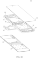
- FIG. 2A illustrates an unfolded state of an exemplary electronic device.
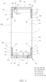
- FIG. 2B illustrates a folded state of an exemplary electronic device.
- FIG. 2C is an exploded view of an exemplary electronic device.
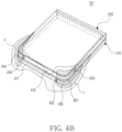
- the first housing 210 may include a first surface 211, a second surface 212 opposites to the first surface 211, and a first side surface 213 surrounding at least a portion of the first surface 211 and the second surface 212.
- the second housing 220 may further include at least one camera 234 exposed through a portion of the second surface 212 and a display panel 235.
- the first housing 210 may provide a space formed by the first surface 211, the second surface 212, and the first side surface 213 as a space for arranging components of the electronic device 101.
- the first side surface 213 and a second side surface 223 may include a conductive material, a non-conductive material, or a combination thereof.
- the first side surface 213 and the second side surface 223 may include a conductive portion 228 and a non-conductive portion 229.
- the conductive portion 228 may include a plurality of conductive members.
- the plurality of conductive members may be spaced apart from each other.
- the non-conductive portion 229 may be disposed between a plurality of conductive members.
- An antenna structure may be formed by some of a plurality of conductive members and a plurality of non-conductive members or a combination thereof.
- the second housing 220 may include a third surface 221, a fourth surface 222 opposite to the third surface 221, and a second side surface 223 surrounding at least a portion of the third surface 221 and the fourth surface 222.
- the fourth surface 222 may further include a rear plate 290 disposed on the fourth surface 222.
- the second side surface 223 may be rotatably (or pivotably) connected to the first side surface 213 through a hinge structure 250 disposed on a hinge cover 255.
- the hinge structure 250 may include a hinge plate.
- the hinge plate may include a first hinge plate and a second hinge plate.
- the first hinge plate may be connected to the first housing 210.
- the second hinge plate may be connected to the second housing 220.
- the second housing 220 may provide a space formed by the third surface 221, the fourth surface 222 opposite the third surface 221, and the side surface 223 surrounding at least a portion of the third surface 221 and the fourth surface 222 as a space for arranging components of the electronic device 101.
- the display 230 may include a window exposed toward the outside.
- the window may protect a surface of the display 230.
- the window may be formed of a transparent member to transfer visual information provided from the display 230 to the outside.
- the window may include a glass material such as ultra-thin glass (UTG) or a polymer material such as polyimide (PI).
- the display 230 may include a first display area 231 disposed on the first surface 211 of the first housing, a second display area 232 disposed on the third surface 221 of the second housing, and a third display area 233 between the first display area 231 and the second display area 232. At least a portion of the third display area 233 may be disposed on the hinge structure 250.
- an opening may be formed in a portion of a screen display area of the display 230, or a recess or an opening may be formed in a support member (e.g., bracket) supporting the display 230.
- the electronic device 101 may include at least one camera aligned with the recess or the opening.
- the first display area 231 may further include at least one camera 236 capable of obtaining an image from the outside through a portion of the first display area 231.
- the electronic device 101 may include at least one camera 236 on a rear surface of the display 230 corresponding to the first display area 231 or the second display area 232 of the display 230.
- At least one camera 236 may be disposed under the display 230 and may be surrounded by the display 230.
- the at least one camera 236 may not be exposed to the outside by being surrounded by the display 230.
- the display 230 may include an opening exposing the at least one camera 236 to the outside.
- the display 230 may further include the rear surface opposite to a front surface.
- the display 230 may be supported by a first support member 215 of the first housing 210 and a second support member 227 of the second housing 220.
- the hinge structure 250 may be configured to rotatably connect the first support member 215 fastened to the first hinge plate and the second support member 227 fastened to the second hinge plate.
- the hinge cover 255 surrounding the hinge structure 250 may be exposed at least partially through a space between the first housing 210 and the second housing 220 while the electronic device 101 is in a folded state.
- the hinge cover 255 may be covered by the first housing 210 and the second housing 220 while the electronic device 101 is in an unfolded state.
- the electronic device 101 may be folded about a folding axis f passing through the hinge cover 255.
- the hinge cover 255 may be disposed between the first housing 210 and the second housing 220 of the electronic device 101 so that the electronic device 101 may be bent, curved, or folded.
- the first housing 210 may be rotatably connected to the second housing 220 through the hinge structure 250 disposed on the hinge cover 255.
- the first housing 210 may rotate about the folding axis f.
- the electronic device 101 may be folded so that the first housing 210 and the second housing 220 face each other by rotating about the folding axis f. In an embodiment, the electronic device 101 may be folded so that the first housing 210 and the second housing 220 are stacked on each other or overlapped with each other.
- the expression "a component faces another component” may be referred to as the component and the other component being disposed in a location in which a direction toward which the component faces and a direction toward which the other component faces are opposite to each other.
- the electronic device 101 may include a first housing 210, a second housing 220, a hinge structure 250, a display 230, a printed circuit board 261, a display panel 235, and a rear plate 290. According to an embodiment, the electronic device 101 may omit at least one of the components or may additionally include another component.
- the hinge structure 250 may include a hinge plate.
- the hinge structure 250 may include a hinge gear enabling the first housing 210 and the second housing 220 to be pivotable.
- a first support member 215 may be partially surrounded by a first side surface 213.
- the first support member 215 may be integrally formed with the first side surface 213.
- a second support member 227 may be partially surrounded by a second side surface 223.
- the second support member 227 may be integrally formed with the second side surface 223.
- the first support member 215 may be formed separately from the first side surface 213.
- the second support member 227 may be formed separately from the second side surface 223.
- a surface of the first support member 215 may be coupled with the display 230. Another surface of the first support member 215 may be coupled with the display panel 235. A surface of the second support member 227 may be coupled with the display 230. Another surface of the second support member 227 may be coupled with the rear plate 290.
- the printed circuit board 261 and the battery may be disposed between a surface formed by the first support member 215 and the second support member 227 and a surface formed by the display panel 235 and the rear plate 290.
- the printed circuit board 261 may be electrically connected to components for implementing various functions of the electronic device 101.
- an electronic device 101 may include a first housing 210, a second housing 220, and/or communication circuitry 401.
- the electronic device 101 may include a first housing 210 and a second housing 220 that may be folded or unfolded with each other.
- the electronic device 101 according to an embodiment may be referred to as a foldable electronic device 101.
- the second housing 220 may rotate with respect to the first housing 210 about a folding axis f.
- the electronic device 101 may include a hinge structure (e.g., the hinge structure 250 of FIG. 2C ).
- the hinge structure 250 may enable the electronic device 101 to be switched to a folded state or an unfolded state by rotatably connecting the first housing 210 and the second housing 220 with respect to the folding axis f.
- the communication circuitry 401 may be disposed in the first housing 210 or the second housing 220.
- the communication circuitry 401 may be disposed on a first printed circuit board 261 in the first housing 210.
- the communication circuitry 401 may be configured to wirelessly communicate with an external electronic device.
- the communication circuitry 401 may be configured to receive a signal from an external electronic device through an antenna and/or transmit a signal to an external electronic device through the antenna.
- the first housing 210 may include a first side member 214 (or a first side bezel) including a first periphery 210a, a second periphery 210b, and a third periphery 210c.
- the first periphery 210a may be perpendicular to the folding axis f.
- the first periphery 210a may include a first non-conductive portion 431.
- the second periphery 210b may be perpendicular to the folding axis f.
- the second periphery 210b may be opposites to the first periphery 210a.
- the third periphery 210c may be spaced apart from the folding axis f.
- the third periphery 210c may be parallel to the folding axis f.
- the third periphery 210c may be disposed between the first periphery 210a and the second periphery 210b.
- the third periphery 210c may extend from an end of the first periphery 210a to an end of the second periphery 210b.
- the third periphery 210c may include a second non-conductive portion 432.
- the second housing 220 may include a second side member 224 (or a second side bezel) including a fourth periphery 220a, a fifth periphery 220b, and a sixth periphery 220c.
- the fourth periphery 220a may be perpendicular to the folding axis f.
- the fourth periphery 220a may include a third non-conductive portion 433.
- the fifth periphery 220b may be perpendicular to the folding axis f.
- the fifth periphery 220b may be opposite to the fourth periphery 220a.
- the sixth periphery 220c may be spaced apart from the folding axis f.
- the sixth periphery 220c may be parallel to the folding axis f.
- the sixth periphery 220c may be disposed between the fourth periphery 220a and the fifth periphery 220b.
- the sixth periphery 220c may extend from an end of the fourth periphery 220a to an end of the fifth periphery 220b.
- the sixth periphery 220c may include a fourth non-conductive portion 434.
- the third periphery 210c may face the sixth periphery 220c.
- the first periphery 210a may face the fifth periphery 220b.
- the second periphery 210b may face the fourth periphery 220a.
- the third periphery 210c may be opposite to the sixth periphery 220c.
- the first periphery 210a may be disposed on substantially the same line as the fifth periphery 220b.
- a first support member 215 may be partially connected to the first side member 214.
- the first support member 215 may be spaced apart from the third periphery 210c.
- the first support member 215 may be connected to a portion of the first periphery 210a.
- the first support member 215 may be spaced apart from another portion of the first periphery 210a.
- a boundary between the portion of the first periphery 210a connected to the first support member 215 and the other portion of the first periphery 210a spaced apart from the first support member 215 may be referred to as a location P3 of FIG. 3 .
- the first support member 215 may be connected to a portion of the second periphery 210b.
- the first support member 215 may be spaced apart from another portion of the second periphery 210b.
- a boundary of the portion of the second periphery 210b connected to the first support member 215 and the other portion of the second periphery 210b spaced apart from the first support member 215 may be referred to as a location P1 of FIG. 3 .
- the second support member 227 may be partially connected to the second side member 224.
- the second support member 227 may be spaced apart from the sixth periphery 220c.
- the second support member 227 may be connected to a portion of the fourth periphery 220a.
- the second support member 227 may be spaced apart from another portion of the fourth periphery 220a.
- a boundary of the portion of the fourth periphery 220a connected to the second support member 227 and the other portion of the fourth periphery 220a connected to the second support member 227 may be referred to as a location P4 of FIG. 3 .
- the second support member 227 may be connected to a portion of the fifth periphery 220b.
- the second support member 227 may be spaced apart from another portion of the fifth periphery 220b.
- a boundary of the portion of the fifth periphery 220b connected to the second support member 227 and the other portion of the fifth periphery 220b connected to the second support member 227 may be referred to as a location P2 of FIG. 3 .
- the first housing 210 and the second housing 220 may include a plurality of conductive portions.
- the first housing 210 may include a first conductive portion 411, a second conductive portion 412, and/or a third conductive portion 413.
- the first conductive portion 411 may extend from a first non-conductive portion 431 to a second non-conductive portion 432.
- the first conductive portion 411 may extend from the first non-conductive portion 431 in the first periphery 210a to the second non-conductive portion 432 in the third periphery 210c along the first periphery 210a and the third periphery 210c.
- the second conductive portion 412 may extend from the second non-conductive portion 432 to a location P1 of the second periphery 210b.
- the second conductive portion 412 may extend from the second non-conductive portion 432 in the third periphery 210c along the third periphery 210c and the second periphery 210b to a location P1 where the second periphery 210b and the first side member 214 are connected.
- the third conductive portion 413 may extend from the first non-conductive portion 431 toward the folding axis f along the first periphery 210a. However, it is not limited thereto.
- the electronic device 101 may include a first opening area 201 disposed between the first side member 214 and the first support member 215 and a second opening area 202 disposed between the second side member 224 and the second support member 227.
- the first opening area 201 and the second opening area 202 may be filled with a non-conductive material.
- the first side member 214 may be spaced apart from the first support member 215 through the first opening area 201 disposed between the first side member 214 and the first support member 215.
- the first opening area 201 may include a first slot S1 and a second slot S2, which are partial areas within the first opening area 201.
- the first slot S1 may be formed between the second conductive portion 412 and the first support member 215.
- an end S1-1 of the first slot S1 may be located between a location P1 in the second periphery 210b and the first support member 215.
- Another end S1-2 of the first slot S1 may be located between an end of the second conductive portion 412 in contact with the second non-conductive portion 432 and the first support member 215.
- the second slot S2 may be disposed between the third conductive portion 413 and the first support member 215.
- an end S2-1 of the second slot S2 may be located between a location P3 in the first periphery 210a and the first support member 215.
- Another end S2-2 of the second slot S2 may be located between an end of the third conductive portion 413 in contact with the first non-conductive portion 431 and the first support member 215.
- the end S1-1 and the other end S1-2 of the first slot S1 and the end S2-1 and the other end S2-2 of the second slot S2 may be referred to as a boundary for distinguishing the first slot S1 and the second slot S2 within the first opening area 201, rather than a physical boundary or including a material different from other portions within the first opening area 201.
- the second housing 220 may include a fourth conductive portion 421, a fifth conductive portion 422, and/or a sixth conductive portion 423.
- the fourth conductive portion 421 may extend from the third non-conductive portion 433 to the fourth non-conductive portion 434.
- the fourth conductive portion 421 may extend from the third non-conductive portion 433 in the fourth periphery 220a to the fourth non-conductive portion 434 in the sixth periphery 220c along the fourth periphery 220a and the sixth periphery 220c.
- the fifth conductive portion 422 may extend from the fourth non-conductive portion 434 to a location P2 of the fifth periphery 220b.
- the fifth conductive portion 422 may extend from the fourth non-conductive portion 434 in the sixth periphery 220c along the sixth periphery 220c and the fourth periphery 220a to the location P2 where the fourth periphery 220a and the second side member 224 are connected.
- the sixth conductive portion 423 may extend from the third non-conductive portion 433 toward the folding axis f along the fourth periphery 220a.
- the second side member 224 may be spaced apart from the second support member 227 through the second opening area 202 disposed between the second side member 224 and the second support member 227.
- the second opening area 202 may include a third slot S3 and a fourth slot S3, which are partial areas within the second opening area 202.
- the third slot S3 may be formed between the sixth conductive portion 423 and the second support member 227.
- an end S3-1 of the third slot S3 may be located between a location P4 in the fourth periphery 220a and the second support member 227.
- another end S3-2 of the third slot S3 may be located between an end of the sixth conductive portion 423 in contact with the third non-conductive portion 433 and the second support member 227.
- the fourth slot S4 may be disposed between the fifth conductive portion 422 and the second support member 227.
- an end S4-1 of the fourth slot S4 may be located between a location P2 in the fifth periphery 220b and the second support member 227.
- Another end S4-2 of the fourth slot S4 may be located between an end of the fifth conductive portion 422 in contact with the fourth non-conductive portion 434 and the second support member 227.
- the end S3-1 and the other end S3-2 of the third slot S3 and the end S4-1 and the other end S4-2 of the fourth slot S4 may be referred to as a boundary for distinguishing the third slot S3 and the fourth slot S4 within the second opening area 202, rather than a physical boundary or including a material different from other portions within the second opening area 202.
- the slots S1, S2, S3, and S4 may include a non-conductive material (e.g., resin and/or polymer).
- the slots S1, S2, S3, and S4 may be understood as a term indicating a non-conductive portion disposed in an opening between conductive portions 410 of the first housing 210 and the first support member 215 and between conductive portions 420 of the second housing 220 and the second support member 227.
- the meaning of the term "slot" is not limited to the term itself and may also be referred to as a slit, an opening, or an opening slit.
- the conductive portions 410 of the first housing 210 and the conductive portions 420 of the second housing 220 may operate as antenna radiators capable of transmitting and/or receiving signals within a designated frequency range.
- the second conductive portion 412 and the first slot S1 may be referred to as a slot antenna capable of transmitting and/or receiving signals.
- a length of the first slot S1 may correspond to a length of the fourth slot S4.
- a length of the second slot S2 may correspond to a length of the third slot S3.
- the communication circuitry 401 may be configured to feed at least one of the conductive portions 410 of the first housing 210 and/or at least one of the conductive portions 420 of the second housing 220.
- the communication circuitry 401 may communicate with an external electronic device, through an antenna including at least one of the conductive portions 410 of the first housing 210 and/or an antenna including at least one of the conductive portions 420 of the second housing 220.
- the third non-conductive portion 433 may be located to overlap the first conductive portion 411.
- the fourth non-conductive portion 434 may be disposed to overlap the second conductive portion 412.
- the communication circuitry 401 may be configured to wirelessly communicate with an external electronic device in the folded state.
- the communication circuitry 401 may be configured to transmit and/or receive a signal with an external electronic device using the electromagnetic interaction.
- the communication circuitry 401 may communicate with an external electronic device through the electromagnetic field.
- the electromagnetic field By the electromagnetic field, the first conductive portion 411, the second conductive portion 412, and the fifth conductive portion 422 may operate as an antenna capable of transmitting and/or receiving signals within a designated frequency band.
- the electronic device 101 may have a structure in which the electromagnetic field may be formed, in the folded state. Since the electronic device 101 may communicate with an external electronic device through the electromagnetic field in the folded state, wireless communication performance may be improved. Since the conductive portions 410 of the first housing 210 and the conductive portions 420 of the second housing 220 do not need to have a structure symmetrical to each other, configuration and design of the electronic device 101 may be facilitated.
- an electromagnetic field formed when the communication circuitry 401 feeds a first conductive portion may have a radiation characteristic by an electromagnetic interaction between conductive portions (e.g., the conductive portions 410 of FIG. 3 ) of a first housing (e.g., the first housing 210 of FIG. 3 ) and conductive portions (e.g., the conductive portions 420 of FIG. 3 ) of a second housing (e.g., the second housing 220 of FIG. 3 ).
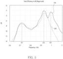
- a radiation current may flow along the first conductive portion 411.
- An electromagnetic field may be formed at the first conductive portion 411 by the radiation current flowing along the first conductive portion 411.
- the first resonant point 511 may be formed by an electromagnetic field formed at the first conductive portion 411.
- the first resonant point 511 may be about 0.7 to 0.8 GHz, but is not limited thereto.
- the processor 120 and/or the communication circuitry 401 may move the third resonant point 513. For example, based on a targeted frequency band, the processor 120 and/or the communication circuitry 401 may move the third resonant point 513 into the frequency band.
- the processor 120 and/or the communication circuitry 401 may adjust impedance of the conductive portions 410 of the first housing 210 and/or the conductive portions 420 of the second housing 220 through impedance matching circuitry (e.g., the impedance matching circuitry 450 of FIG. 3 ). As the impedance of the conductive portions 410 and 420 is adjusted, the third resonant point 513 may be moved.
- the electronic device 101 may communicate with an external electronic device using an electromagnetic field coupled to the first slot S1 and the fourth slot S4.
- the processor 120 and/or the communication circuitry 401 may adjust the third resonant point 513 through impedance matching circuitry (e.g., the impedance matching circuitry 450 of FIG. 3 ).
- the processor 120 and/or the communication circuitry 401 may move (e.g., out-band) the first resonant point 511 out of a targeted frequency band through the impedance matching circuitry 450 when communicating with an external electronic device based on the third resonant point 513.
- An example of an operation in which the processor 120 and/or the communication circuitry 401 adjusts the impedance matching circuitry 450 for tuning the third resonant frequency will be illustrated through FIGS. 6A , 6B , and 6C .
- an electronic device may be referred to as an electronic device having a structure in which conductive portions of the first housing and conductive portions of the second housing correspond to each other in the folded state.
- non-conductive portions e.g., the first non-conductive portion 431, the second non-conductive portion 432, the third non-conductive portion 433, or the fourth non-conductive portion 434 included in the first housing and the second housing may be disposed to overlap each other.
- the coupled third resonant point 513 may not be formed.
- the third resonant point by coupling of an electromagnetic field is not formed.
- a gain of the signal having the frequency in the lower band may be lower than that of the first graph 510.
- the electronic device 101 may have a structure capable of forming an electromagnetic field in the first slot S1 and the fourth slot S4 when feeding the first conductive portion 421 of the first housing 210 in the folded state. According to an embodiment, within the low band, the wireless communication performance (e.g., sensitivity or bandwidth) of the electronic device 101 may be improved.
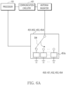
- FIG. 6A is a simplified block diagram of an exemplary electronic device.
- FIG. 6B is a graph illustrating a radiation characteristic of an electronic device by adjusting an impedance value of conductive portions in a folded state of an exemplary electronic device.
- FIG. 6C is a graph illustrating a radiation characteristic of an electronic device by adjusting an impedance value of a first conductive portion in a folded state of an exemplary electronic device.
- an electronic device 101 may include at least one processor 120 and communication circuitry 401 for wireless communication with an external electronic device.
- the communication circuitry 401 may include a radio frequency front end (RFFE).
- RFFE radio frequency front end
- the communication circuitry 401 may provide an antenna radiator with a signal to be transmitted to an external electronic device.
- the communication circuitry 401 may obtain a signal received from the external electronic device to an antenna radiator.
- a first conductive portion (e.g., the first conductive portion 411 of FIG. 3 ), a second conductive portion (e.g., the second conductive portion 412 of FIG. 3 ), a fourth conductive portion (e.g., the fourth conductive portion 421 of FIG. 3 ), and/or a fifth conductive portion (e.g., the fifth conductive portion 422 of FIG. 3 ) may operate as an antenna radiator by being fed by the communication circuitry 401.
- the antenna radiator of FIG. 6A may be referred to as at least one of the conductive portions.
- At least one processor 120 may transmit a signal to the external electronic device through the first conductive portion 411, the second conductive portion 412, the fourth conductive portion 421, and/or the fifth conductive portion 422.
- at least one processor 120 may receive a signal through the first conductive portion 411, the second conductive portion 412, the fourth conductive portion 421, and/or the fifth conductive portion 422.
- the at least one processor 120 may be referred to as the processor 120 of FIG. 1 or a communication processor (CP).
- the electronic device 101 may include impedance matching circuitry 450 configured to adjust a resonant frequency of an antenna by adjusting an impedance value of the first conductive portion 411, the second conductive portion 412, the fourth conductive portion 421, and/or the fifth conductive portion 422.
- the electronic device 101 may include first impedance matching circuitry 451 electrically connected to the first conductive portion 411, second impedance matching circuitry 452 electrically connected to the second conductive portion 412, third impedance matching circuitry 453 electrically connected to the fourth conductive portion 421, and/or fourth impedance matching circuitry 454 electrically connected to the fifth conductive portion 422.
- the at least one processor 120 may adjust a resonant frequency of an antenna through the impedance matching circuitry 450.
- the first impedance matching circuitry 451 may include at least one aperture tuner 451a and a switch SW connectable to the at least one aperture tuner 451a to adjust an impedance value of the first conductive portion 411.
- the at least one aperture tuner 451a may include a plurality of passive components connectable to the switch SW.
- the at least one aperture tuner 451a may include a plurality of capacitors each having a designated capacitance value and/or a plurality of inductors each having a designated inductance value.
- the first impedance matching circuitry 451 may include four capacitors having different capacitance values.
- the switch SW may be a single pole four throw (SP4T) switch capable of electrically connecting any one of the four capacitors with the first conductive portion 411.
- SP4T single pole four throw
- the first impedance matching circuitry 451 may be variously implemented.
- the switch SW may include a single pole single throw (SPST) switch, a single pole double throw (SPDT), or a single pole triple throw (SP3T).
- the first impedance matching circuitry 451 may include one or more switches.
- at least one aperture tuner 451a may include a variable capacitor having an adjustable capacitance value and/or a variable inductor having an adjustable inductance value.
- the first impedance matching circuitry 451 may be operably connected to the at least one processor 120.
- the at least one processor 120 may be configured to adjust an impedance value of the first conductive portion 411 by controlling the switch SW to be connected to the at least one aperture tuner 451a.
- the at least one processor 120 may identify a resonant frequency of a transmission signal through the communication circuitry 401. When the identified resonant frequency is different from a designated frequency, the at least one processor 120 may electrically connect the first conductive portion 411 to at least one of the plurality of passive components included in the matching circuitry 451 by controlling the switch SW.
- the resonant frequency of the transmission signal may be adjusted.
- the descriptions of the first impedance matching circuitry 451 may be applied substantially equally to the second impedance matching circuitry 452 electrically connected to the second conductive portion 412, the third impedance matching circuitry 453 electrically connected to the fourth conductive portion 421, and the fourth impedance matching circuitry 454 electrically connected to the fifth conductive portion 422.
- configurations of the first impedance matching circuitry to the fourth impedance matching circuitry 454 may be variously configured based on a resonant frequency of an antenna.
- the at least one processor 120 may be configured to adjust a radiation characteristic of the electronic device 101 through the impedance matching circuitry 450 in the folded state.
- the at least one processor 120 may electrically connect a switch SW in the first impedance matching circuitry 451 to a passive component having a first impedance value, electrically connect a switch SW in the second impedance matching circuitry 452 to a passive component having a second impedance value, and electrically connect a switch SW in the third impedance matching circuitry 453 to a passive component having a third impedance value.
- an impedance value of the first impedance matching circuitry 451 may be indicated as the first impedance value.
- the communication circuitry 401 may be configured to communicate with an external electronic device by using a third resonant point (e.g., the third resonant point 513 of FIG. 5 ) formed by slots (e.g., the first slot S1, the second slot S2, the third slot S3, and/or the fourth slot S4), conductive portions (e.g., the conductive portions 410 and 420 of FIG. 3 ) and/or non-conductive portions (e.g., the first non-conductive portion 431, the second non-conductive portion 432, the third non-conductive portion 433, and/or the fourth non-conductive portion 434) of the electronic device 101.
- a third resonant point e.g., the third resonant point 513 of FIG. 5
- slots e.g., the first slot S1, the second slot S2, the third slot S3, and/or the fourth slot S4
- conductive portions e.g., the conductive portions 410 and 420 of FIG. 3
- non-conductive portions e.g
- the first impedance matching circuitry 451 electrically connected to the first conductive portion 411 may be used to move a first resonant point (e.g., the first resonant point 511 of FIG. 5 ) out of a designated frequency band (e.g., low band).
- a designated frequency band e.g., low band
- the at least one processor 120 may move the first resonant point 511 out of the band.
- the electronic device 101 may transmit and/or receive a signal within the designated frequency band using the third resonant point 513.
- the first impedance matching circuitry 451 electrically connected to the first conductive portion 411 may be used to adjust a frequency band of the third resonant point 513.
- the first impedance matching circuitry 451 may adjust an impedance value of the first conductive portion 411 that is fed from the communication circuitry 401.
- a frequency of the third resonant point 513 may be adjusted according to the impedance value of the first conductive portion 411.
- the at least one processor 120 may control the first impedance matching circuitry 451 so that the third resonant point 513 is located within a designated frequency band.
- the at least one processor 120 may be configured to control the second impedance matching circuitry 452 electrically connected to the second conductive portion 412 and/or the fourth impedance matching circuitry 454 electrically connected to the fifth conductive portion 422 for tuning a third resonant point (e.g., the third resonant point 513 of FIG. 5 ).
- Graphs 600 of FIG. 6B indicate a change in radiation characteristic of an electronic device (e.g., the electronic device 101 of FIG. 3 ) when changing a second impedance value of the second impedance matching circuitry (e.g., the second impedance matching circuitry 452 of FIG. 3 ) and/or a fourth impedance value of the fourth impedance matching circuitry 454 in a state that a first impedance value of the first impedance matching circuitry 600 is fixed.
- a first graph 601 illustrates a radiation characteristic of the electronic device 101 when the first impedance value is 1.5 pF, the second impedance value is 1.5 pF, and the fourth impedance value is 1.5 pF.
- a second graph 602 illustrates a radiation characteristic of the electronic device 101 when the first impedance value is 1.5 pF, the second impedance value is 2.2 pF, and the fourth impedance value is 2.2 pF.
- a third graph 603 illustrates a radiation characteristic of the electronic device 101 when the first impedance value is 1.5 pF, the second impedance value is 2.7 pF, and the third impedance value is 2.7 pF.
- a fourth graph 604 illustrates a radiation characteristic of the electronic device 101 when the first impedance value is 1.5 pF, the second impedance value is 0.5 pF, and the fourth impedance value is 100nH.
- a fifth graph 605 illustrates a radiation characteristic of the electronic device 101 when the first impedance value is 1.5 pF, the second impedance value is 1.5 pF, and the fourth impedance value is 100nH.
- a sixth graph 606 illustrates a radiation characteristic of the electronic device 101 when the first impedance value is 1.5 pF, the second impedance value is 100nH, and the sixth impedance value is 100nH.
- an electromagnetic field (e.g., the electromagnetic field F of FIG. 4C ) formed by an electromagnetic interaction among conductive portions (e.g., the conductive portions 410 of FIG. 3 ) of a first housing (e.g., the first housing 210 of FIG. 3 ), conductive portions (e.g., the conductive portions 420 of FIG. 3 ) of a second housing (e.g., the second housing 220 of FIG. 3 ), and slots (e.g., the first slot S1, the second slot S2, the third slot S3, and/or the fourth slot S4 of FIG.
- conductive portions e.g., the conductive portions 410 of FIG. 3
- a first housing e.g., the first housing 210 of FIG. 3
- conductive portions e.g., the conductive portions 420 of FIG. 3
- slots e.g., the first slot S1, the second slot S2, the third slot S3, and/or the fourth slot S4 of FIG.
- the at least one processor 120 may adjust a radiation characteristic of an antenna using an electromagnetic field formed on the first slot S1 and the fourth slot S4 by adjusting impedance values of the second conductive portion 412 and the fifth conductive portion 422 in the folded state.
- the at least one processor 120 adjusts a second impedance value and a fourth impedance value
- the radiation characteristic of the electronic device 101 in the folded state may be referred to as a first sweep graph G1.
- a second sweep graph G2 of FIG. 6B illustrates a radiation characteristic of the electronic device 101 using an electromagnetic field formed at the first conductive portion 411 when the electronic device according to a comparative example having a structure in which conductive portions of the first housing 210 and conductive portions of the second housing 220 correspond to each other is in folded state.
- the electronic device according to the comparative example may be disposed so that non-conductive portions (e.g., the first non-conductive portion 431, the second non-conductive portion 432, the third non-conductive portion 433, or the fourth non-conductive portion 434) included in the first housing and the second housing overlap each other.
- the first sweep graph G1 may have a higher gain than the second sweep graph G2 in a frequency band between about 0.65 GHz and about 1.0 GHz.
- the electronic device 101 may communicate with an external electronic device using a third resonant point (e.g., the third resonant point 513 of FIG. 5 ) in the folded state, the electronic device 101 according to an embodiment may have improved wireless communication performance.
- a third resonant point e.g., the third resonant point 513 of FIG. 5
- the at least one processor 120 may be configured to adjust a radiation characteristic of the electronic device 101 in the folded state through third impedance matching circuitry (e.g., the third impedance matching circuitry 454 of FIG. 3 ).
- the at least one processor 120 may electrically connect a switch SW in the third impedance matching circuitry 453 to a passive component having a third impedance value.
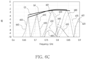
- the graphs of FIG. 6C illustrate a change in radiation characteristic of the electronic device 101 when a fourth conductive portion (e.g., the fourth conductive portion 421 of FIG. 3 ) is electrically connected to the passive component having the third impedance value.
- a first graph 601 illustrates a radiation characteristic of the electronic device 101 when at least one aperture tuner 451a and the fourth conductive portion 421 in the third impedance matching circuitry 453 are electrically separated in a first state in which the first impedance value is 1.5pF, the second impedance value is 1.5pF, and the fourth impedance value is 1.5pF.
- a second graph 620 indicates a radiation characteristic of the electronic device 101 when the third impedance value is 27nH in the first state.
- a third graph 630 illustrates a radiation characteristic of the electronic device 101 when at least one aperture tuner 451a in the third impedance matching circuitry 453 and the fourth conductive portion 421 are electrically separated in a second state in which the first impedance value is 1.5 pF, the second impedance value is 2.2 pF, and the fourth impedance value is 2.2 pF.
- a fourth graph 640 illustrates a radiation characteristic of the electronic device 101 when the third impedance value is 27nH in the second state.
- a fifth graph 650 illustrates a radiation characteristic of the electronic device 101 when at least one aperture tuner 451a in the third impedance matching circuitry 453 and the fourth conductive portion 421 are electrically separated in a third state in which the first impedance value is 1.5 pF, the second impedance value is 2.7 pF, and the fourth impedance value is 2.7 pF.
- a sixth graph 660 illustrates a radiation characteristic of the electronic device 101 when the third impedance value is 27nH in the third state.
- a seventh graph 670 illustrates a radiation characteristic of the electronic device 101 when at least one aperture tuner 451a in the third impedance matching circuitry 453 and the fourth conductive portion 421 are electrically separated in a fourth state in which the first impedance value is 1.5 pF, the second impedance value is 1.0 pF, and the fourth impedance value is 100nH.
- the eighth graph 680 illustrates a radiation characteristic of the electronic device 101 when the third impedance value is 27nH in the fourth state.
- the radiation characteristic of the electronic device 101 may be precisely adjusted through the third impedance matching circuitry 453 electrically connected to the fourth conductive portion 421.
- the at least one processor 120 may adjust the radiation characteristic of the electronic device 101 using an electromagnetic field formed on the first slot S1 and the fourth slot S4 by adjusting an impedance value of the fourth conductive portion 421 through the third impedance matching circuitry 453.
- the radiation characteristic of the electronic device 101 in the folded state may be referred to as a first sweep graph G3 based on the third impedance value.
- a second sweep graph G4 of FIG. 6C illustrates a radiation characteristic of the electronic device 101 in the folded state when the fourth conductive portion 421 and at least one aperture tuner 451a in the third impedance matching circuitry 453 are electrically separated. Comparing the first sweep graph G3 and the second sweep graph G4, the electronic device 101 according to an embodiment may improve about 0.5 dB radiation efficiency by adjusting the fourth impedance value within a frequency range of about 600 MHz to about 700 MHz.
- the electronic device 101 according to an embodiment may have improved wireless communication performance as a transmission and/or reception gain of a wireless communication signal is improved.
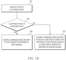
- FIG. 7A schematically illustrates an exemplary electronic device.
- FIG. 7B is a flowchart illustrating an operation of at least one processor performed based on a state of an electronic device.
- a first support member 215 may be spaced apart from a first conductive portion 411, a second conductive portion 412, and a third conductive portion 413.
- a second support member 227 may be spaced apart from a fourth conductive portion 421, a fifth conductive portion 422, and a sixth conductive portion 423.
- the electronic device 101 may include a non-conductive member disposed between the first support member 215 and a first side member 214 and between the second support member 227 and a second side member 224.
- the non-conductive member may electrically separate the first support member 215 and the first side member 214 and electrically separate the second support member 227 and the second side member 224.
- the electronic device 101 may include a first slot S1, a second slot S2, a third slot S3, and a fourth slot S4.
- the first slot S1, the second slot S2, the third slot S4, and the fourth slot S4 may include a non-conductive material (e.g., resin).
- the electronic device 101 may include a fifth non-conductive portion 435 disposed at a second periphery 210b of the first housing 210 and a sixth non-conductive portion 436 disposed at a fifth periphery 220b of the second housing 220.
- the second conductive portion 412 may be separated into a seventh conductive portion 412a and an eighth conductive portion 412b by the fifth non-conductive portion 435.
- the seventh conductive portion 412a may extend from the second non-conductive portion 432 in a third periphery 210c to the fifth non-conductive portion 435 in the second periphery 210b.
- the eighth conductive portion 412b may extend from the fifth non-conductive portion 435 in the second periphery 210b to a location P1 of the second periphery 210b along the second periphery 210b.
- the fifth conductive portion 422 may be separated into a ninth conductive portion 422a and a tenth conductive portion 422b by the sixth non-conductive portion 436.
- the ninth conductive portion 422a may extend from the fourth non-conductive portion 434 in a sixth periphery 220c to the sixth non-conductive portion 436 in the fifth periphery 220b.
- the tenth conductive portion 422b may extend from the sixth non-conductive portion 436 in the fifth periphery 220b to a location P2 of the fifth periphery 220b along the fifth periphery 220b.
- the electronic device 101 may include a first switch SW1 and/or a second switch SW2.
- the first switch SW1 may electrically connect the seventh conductive portion 412a and the eighth conductive portion 412b.
- the second switch SW2 may electrically connect the ninth conductive portion 422a and the tenth conductive portion 422b.
- the first switch SW1 and the second switch SW2 may be operably connected to the communication circuitry 401.
- the communication circuitry 401 may electrically connect or electrically separate the seventh conductive portion 412a and the eighth conductive portion 412b.
- the communication circuitry 401 may electrically connect or electrically separate the ninth conductive portion 422a and the tenth conductive portion 422b.
- the communication circuitry 401 may variously implement a resonant frequency of an antenna through the first switch SW1 and the second switch SW2.
- the communication circuitry 401 may be configured to control the first switch SW1 and the second switch SW2, based on a resonant frequency of a signal to be transmitted to an external electronic device in the folded state. For example, when feeding the first conductive portion 411, the communication circuitry 401 may adjust an electrical length of an antenna including the second conductive portion 412 and/or an antenna including the fifth conductive portion 422, through the first switch SW1 and/or the second switch SW2.
- the communication circuitry 401 may adjust a resonant frequency of an antenna including the second conductive portion 412 and/or a resonant frequency of an antenna including the fifth conductive portion 422, by adjusting the electrical length of the antenna including the second conductive portion 412 and/or the antenna including the fifth conductive portion 422.
- the communication circuitry 401 may be configured to, based on a state of the electronic device 101, feed a conductive portion (e.g., the first conductive portion 411) of the first housing 210, or feed at least one of the conductive portions 410 of the first housing 210 and/or at least one of the conductive portions 420 of the second housing 220.
- a conductive portion e.g., the first conductive portion 4111
- the communication circuitry 401 may be configured to, based on a state of the electronic device 101, feed a conductive portion (e.g., the
- At least one processor 120 may control the communication circuitry 401 to feed a conductive portion (e.g., the first conductive portion 411) of the first housing 210, based on the folded state of the electronic device 101. Since the folded state is a state in which the first housing 210 and the second housing 220 face each other, a distance between the sensor 461 and the magnet 462 may be the closest. In the folded state, the magnitude of a magnetic field of the magnet 462 obtained through the sensor 461 may be within a first range. The at least one processor 120 may identify that the electronic device 101 is in the folded state, based on identifying that the magnitude of the magnetic field of the magnet 462 indicated by the data obtained through the sensor 461 is included within the first range.
- a conductive portion e.g., the first conductive portion 4111
- the at least one processor 120 may adjust a resonant frequency of the antenna within a designated frequency band, through the first impedance matching circuitry 451 electrically connected to the first conductive portion 411.
- the at least one processor 120 may tune the resonant frequency of the antenna through the second impedance matching circuitry 452 and/or the fourth impedance matching circuitry 454.
- tuning of the resonant frequency of the antenna by the second impedance matching circuitry 452 and the fourth impedance matching circuitry 454 may be referred to as the description described with reference to FIG. 6B .
- the at least one processor 120 may precisely adjust the resonant frequency of the antenna through the third impedance matching circuitry 453.
- tuning of the resonant frequency of the antenna by the third impedance matching circuitry 453 may be referred to as the description described with reference to FIG. 6C .
- the communication circuitry 401 may transmit a signal having a frequency in the low band to an external electronic device, or receive a signal having a frequency in the low band from an external electronic device.
- the at least one processor 120 may adjust a resonant frequency of an antenna including the first conductive portion 411, through the first impedance matching circuitry 451 electrically connected to the first conductive portion 411.
- the at least one processor 120 may adjust a resonant frequency of an antenna including the fourth conductive portion 421, through the third impedance matching circuitry 453 electrically connected to the fourth conductive portion 421.
- the fourth conductive portion 421 may be used as an antenna radiator for transmitting and/or receiving a signal with a frequency within the low band.
- the fourth conductive portion 421 may be used as an antenna radiator for a transmission diversity (Drx: diversity Rx).
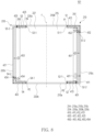
- FIG. 8 schematically illustrates an exemplary electronic device.
- the electronic device 101 may have peripheries (e.g., the first periphery 210a, the second periphery 210b, the fourth periphery 220a, and the fifth periphery 220b of FIG. 3 ) perpendicular to a folding axis f longer than peripheries (e.g., the third periphery 210c and the sixth periphery 220c of FIG. 3 ) parallel to the folding axis f, but are not limited thereto.
- peripheries e.g., the first periphery 210a, the second periphery 210b, the fourth periphery 220a, and the fifth periphery 220b of FIG. 3
- peripheries e.g., the third periphery 210c and the sixth periphery 220c of FIG. 3
- the peripheries in the unfolded state, the peripheries may be substantially the same or similar. Accordingly, redundant descriptions may be
- the electronic device 101 may include non-conductive portions that do not overlap each other and are spaced apart from each other in the folded state.
- the first housing 210 may include a first non-conductive portion 431 and a second non-conductive portion 432.
- the second housing 220 may include a third non-conductive portion 433 and a fourth non-conductive portion 434.
- the first non-conductive portion 431 may be disposed to overlap the fifth conductive portion 422.
- the second non-conductive portion 432 may be disposed to overlap the fourth conductive portion 421.
- the third non-conductive portion 433 may be disposed to overlap the second conductive portion 412.
- the fourth non-conductive portion 434 may be disposed to overlap the first conductive portion 411.
- the electronic device 101 may include a first slot S1 between the second conductive portion 412 and the first support member 215, a second slot S2 between the third conductive portion 413 and the first support member 215, a third slot S3 between the sixth conductive portion 423 and the second support member 217, and a fourth slot S4 between the fifth conductive portion 422 and the second support member 227.
- the communication circuitry 401 may be configured to feed the first conductive portion 411. As the first conductive portion 411 is fed, an electromagnetic field may be formed in the first conductive portion 411. The electromagnetic field formed at the first conductive portion 411 may be excited to the first slot S1 and the fourth slot S4.
- the electronic device 101 may communicate with an external electronic device using a third resonant point by the electromagnetic field excited to the first slot S1 and the fourth slot S4.
- wireless communication performance of the electronic device 101 may be improved.
- An electronic device may include a first housing (e.g., the first housing 210 of FIG. 3 ), a second housing (e.g., the second housing 220 of FIG. 3 ), and communication circuitry (e.g., the communication circuitry 401 of FIG. 3 ).
- the first housing 210 may include a first periphery (e.g., the first periphery 210a of FIG. 3 ), a second periphery (e.g., the second periphery 210b of FIG. 3 ), and a third periphery (e.g., the third periphery 210c of FIG. 3 ).
- the first periphery 210a may be perpendicular to a folding axis f.
- the first periphery 210a may include a first non-conductive portion (e.g., the first non-conductive portion 431 of FIG. 3 ).
- the second periphery 210b may be opposite to the first periphery 210a.
- the third periphery 210c may be parallel to the folding axis f.
- the third periphery 210c may include a second non-conductive portion (e.g., the second non-conductive portion 432 of FIG. 3 ).
- the third periphery 210c may be disposed between the first periphery 210a and the second periphery 210b.
- the sixth periphery 220c may be parallel to the folding axis f.
- the sixth periphery 220c may include a fourth non-conductive portion (e.g., the fourth non-conductive portion 434 of FIG. 3 ).
- the sixth periphery 220c may be disposed between the fourth periphery 220a and the fifth periphery 220b.
- the second housing 220 may rotate with respect to the first housing 210 about the folding axis f. In a folded state in which the third periphery 210c and the sixth periphery 220c face each other, the first periphery 210a may face the fifth periphery 220b.
- the first housing 210 may include a first conductive portion (e.g., the first conductive portion 411 of FIG. 3 ), a second conductive portion (e.g., the second conductive portion 412 of FIG. 3 ), and a first slot (e.g., the first slot S1 of FIG. 3 ).
- the first conductive portion 411 may extend from the second non-conductive portion 432 to the second non-conductive portion 432.
- the second conductive portion 412 may extend from the second non-conductive portion 432 to a location P1 of the second periphery 210b.
- the first slot S1 may be disposed between the second conductive portion 412 and a first support member 215 in the first housing 210.
- the second housing 220 may include a third conductive portion (e.g., the fifth conductive portion 422 of FIG. 3 ) and a second slot (e.g., the fourth slot S4 of FIG. 3 ).
- the third conductive portion 422 may extend from the fourth non-conductive portion 434 to a location P2 of the fifth periphery 220b.
- the second slot S2 may be disposed between the third conductive portion 422 and a second support member 227 in the second housing 220.
- the communication circuitry 401 may be configured to communicate with an external electronic device using an electromagnetic field formed at the first slot S1 and the second slot S4, based on feeding the first conductive portion 411 in the folded state.
- conductive portions of the first housing, conductive portions of the second housing, and the slots may be disposed to electromagnetically interact with each other when the communication circuitry feeds the first conductive portion in the folded state.
- the electronic device In the folded state, the electronic device may communicate with an external electronic device using an electromagnetic field formed on the first slot and the second slot. Since the electromagnetic field may form resonance (e.g., a third resonant point) by coupling, wireless communication performance of the electronic device may be improved.
- the conductive portions of the first housing and the conductive portions of the second housing do not need to have a structure symmetrical to each other, configuration and design of the electronic device may be simplified.
- the first housing 210 may include a fourth conductive portion (e.g., the fourth conductive portion 413 of FIG. 3 ).
- the fourth conductive portion 413 may extend along the first periphery 210a from the first non-conductive portion 431 toward the folding axis f.
- the second housing 220 may include a fifth conductive portion (e.g., the fourth conductive portion 421 of FIG. 3 ) and a sixth conductive portion (e.g., the sixth conductive portion 423 of FIG. 3 ).
- the fifth conductive portion 421 may extend from the third non-conductive portion 433 to the fourth non-conductive portion 434.
- the sixth conductive portion 423 may extend along the fourth periphery 220a from the fourth non-conductive portion 434 toward the folding axis f.
- the first housing and the second housing may include a plurality of conductive portions and a plurality of non-conductive portions disposed between the plurality of conductive portions.
- the electronic device In the unfolded state, the electronic device may use at least one of the plurality of conductive portions as an antenna radiator.
- the communication circuitry may use an electromagnetic field formed at the first slot and the second slot by a segmentation structure formed by the plurality of conductive portions and the plurality of non-conductive portions.
- the first non-conductive portion 431 may be located to overlap the third conductive portion 422.
- the second non-conductive portion 432 may be located to overlap the fifth conductive portion 421.
- the third non-conductive portion 433 may be located to overlap the first conductive portion 411.
- the fourth non-conductive portion 434 may be positioned to overlap the second conductive portion 412.
- a segmental structure of the first housing and a segmental structure of the second housing may form an electromagnetic field in the first slot and the second slot.
- the electronic device may, by using the electromagnetic field, receive a signal from an external electronic device or transmit a signal to an external electronic device. As the slots and the electromagnetic field are used, radiation performance (e.g., gain) of the electronic device may be improved.
- the first housing 210 may include a third slot (e.g., the second slot S2 of FIG. 3 ).
- the third slot S2 may be disposed between the fourth conductive portion 413 and the first support member 215.
- the second housing 220 may include a fourth slot (e.g., the third slot S3 of FIG. 3 ).
- the fourth slot S3 may be disposed between the sixth conductive portion 423 and the second support member 227.
- slots of an electronic device may form a slot antenna with the conductive portions of the first housing and the conductive portions of the second housing.
- the electronic device may be configured to communicate with an external electronic device using the slot antenna.
- the first conductive portion 411, the second conductive portion 412, and the third conductive portion 422 may operate as at least a portion of an antenna when the communication circuitry 401 feeds the first conductive portion 411 in the folded state.
- the first conductive portion, the second conductive portion, and the third conductive portion may operate as an antenna radiator using an electromagnetic field formed at the first slot and the second slot.
- the first slot S1, the second slot S2, the third slot S3, and the fourth slot S4 may include a non-conductive material (e.g., resin).
- the length of the slots may have a length based on a wavelength according to permittivity of the non-conductive material and a frequency of a signal, but is not limited thereto.
- the communication circuitry 401 may be configured to transmit a signal to an external electronic device, based on feeding at least one of the first conductive portion 411, the second conductive portion 412, the third conductive portion 422, and the fifth conductive portion 421.
- the electronic device in the unfolded state, may use the first conductive portion, the second conductive portion, the third conductive portion, and/or the fifth conductive portion as an antenna. According to an embodiment, various antenna combinations may be possible.
- the first housing 210 may include a fifth non-conductive portion (e.g., the fifth non-conductive portion of FIG. 7A ).
- the fifth non-conductive portion 435 may be disposed at the second periphery 210b.
- the fifth non-conductive portion 435 may separate the second conductive portion 412 into a seventh conductive portion (e.g., the seventh conductive portion 412a of FIG. 7A ) and an eighth conductive portion (e.g., the eighth conductive portion 412b of FIG. 7A ).
- the second housing 220 may include a sixth non-conductive portion (e.g., the sixth non-conductive portion 436 of FIG. 7A ).
- the sixth non-conductive portion 436 may be disposed at the fifth periphery 220b, and may separate the fifth conductive portion 422 into a ninth conductive portion 422a and a tenth conductive portion 422b.
- the electronic device 101 may further include a first switch (e.g., the first switch SW1 of FIG. 7A ), a second switch (e.g., the second switch SW2 of FIG. 7A ), and at least one processor (e.g., the at least one processor 120 of FIG. 6A ).
- the first switch SW1 may electrically connect the seventh conductive portion 412a and the eighth conductive portion 412b.
- the second switch SW2 may electrically connect the ninth conductive portion 422a and the tenth conductive portion 422b.
- the at least one processor 120 may be configured to control a first switch SW1 or a second switch SW2.
- the electronic device may transmit and/or receive various signals. Since a radiation characteristic (e.g., resonant frequency) varies according to a length of the antenna radiator, the electronic device may include an antenna capable of transmitting and/or receiving various signals through a plurality of conductive portions.
- at least one processor may control the first switch and the second switch to adjust the electrical length of the antenna radiator. As the electrical length of the antenna radiator is adjusted, the radiation characteristic of the antenna may be adjusted.
- the electronic device 101 may further include first impedance matching circuitry (e.g., the first impedance matching circuitry 451 of FIG. 3 ) and at least one processor 120.
- the first impedance matching circuitry 451 may be electrically connected to the first conductive portion 411.
- the at least one processor 120 may be configured to adjust a resonant frequency of an antenna including the first conductive portion 411, the second conductive portion 412, and the third conductive portion 422 within a designated frequency band, through the first impedance matching circuitry 451.
- the communication circuitry in the folded state, may feed the first conductive portion.
- the first impedance matching circuitry electrically connected to the first conductive portion may adjust a resonant frequency band of an antenna including the first conductive portion.
- the at least one processor may control the first impedance matching circuitry so that the resonant frequency of the antenna including the first conductive portion is included within a designated frequency band.
- the electronic device 101 may further include second impedance matching circuitry (e.g., the second impedance matching circuitry 452 of FIG. 3 ), third impedance matching circuitry (e.g., the fourth impedance matching circuitry 454 of FIG. 3 ), and at least one processor 120.
- the second impedance matching circuitry 452 may be electrically connected to the second conductive portion 412.
- the third impedance matching circuitry 454 may be electrically connected to the third conductive portion 422.
- the at least one processor 120 may be configured to adjust a resonant frequency of an antenna including the first conductive portion 411, the second conductive portion 412, and the third conductive portion 422, through the second impedance matching circuitry 452 and the third impedance matching circuitry 454.
- the first conductive portion, the second conductive portion, and the third conductive portion may operate as an antenna radiator.
- the antenna including the first conductive portion, the second conductive portion, and the third conductive portion may transmit and/or receive a signal with an external electronic device using an electromagnetic field formed at the first slot and the second slot.
- At least one processor may control the second impedance matching circuitry and the third impedance matching circuitry to adjust the resonant frequency of the antenna.
- a third resonant point may be swept by the second impedance matching circuitry and the third impedance matching circuitry.
- the electronic device 101 may further include fourth impedance matching circuitry (e.g., the third impedance matching circuitry 453 of FIG. 3 ) and at least one processor 120.
- the fourth impedance matching circuitry 453 may be electrically connected to the fifth conductive portion 421.
- the at least one processor 120 may be configured to adjust a resonant frequency of an antenna including the first conductive portion 411, the second conductive portion 412, and the third conductive portion 422, through the fourth impedance matching circuitry 453, in the folded state.
- the fourth impedance matching circuitry electrically connected to the fifth conductive portion may adjust impedance of the fifth conductive portion. In the unfolded state, the fifth conductive portion may operate as an antenna radiator.
- the fourth impedance matching circuitry may be used to adjust a resonant frequency of an antenna including the fifth conductive portion. Since the fifth conductive portion may at least partially face the first conductive portion in the folded state, at least one processor may finely adjust a resonant frequency of an antenna including the first conductive portion, the second conductive portion, and the third conductive portion, through the fourth impedance matching circuitry.
- the electronic device may further include a sensor (e.g., the sensor 461 of FIG. 7A ) and the at least one processor 120.
- the sensor 461 may be used to identify the folded state or an unfolded state different from the folded state.
- the at least one processor 120 may be configured to control the communication circuitry 401 to feed the first conductive portion 411, based on identifying the unfolded state through data obtained from the sensor 461.
- the at least one processor 120 may be configured to control the communication circuitry 401 to feed the first conductive portion 411 or the fifth conductive portion 421, based on identifying the folded state through the sensor 461.
- the electronic device may adjust a feeding location based on a state of the electronic device.
- the communication circuitry may feed the conductive portion (e.g., the first conductive portion) of the first housing. Since the electromagnetic interaction between the conductive portions of the first housing and the conductive portions of the second housing is reduced in the unfolded state, the electronic device may communicate with an external electronic device by feeding at least one (e.g., the first conductive portion) of the conductive portions of the first housing and/or at least one (e.g., the third conductive portion) of the conductive portions of the second housing. In the unfolded state, the at least one processor may be configured to communicate with an external electronic device through an optimal antenna.
- the electronic device 101 may further include a hinge structure (e.g., the hinge structure 250 of FIG. 2C ).
- the hinge structure 250 may enable the electronic device 101 to be switched to the folded state or an unfolded state different from the folded state, by rotatably connecting the first housing 210 and the second housing 220 with respect to the folding axis.
- the electronic device 101 may include a first housing (e.g., the first housing 210 of FIG. 3 ), a second housing (e.g., the second housing 220 of FIG. 3 ), and communication circuitry (e.g., the communication circuitry 401 of FIG. 3 ).
- the first housing 210 may include a first periphery (e.g., the first periphery 210a of FIG. 3 ), a second periphery (e.g., the second periphery 210b of FIG. 3 ), and a third periphery (e.g., the third periphery 210c of FIG. 3 ).
- the first periphery 210a may be perpendicular to a folding axis f.
- the first periphery 210a may include a first non-conductive portion (e.g., the first non-conductive portion 431 of FIG. 3 ).
- the second periphery 210b may be opposite to the first periphery 210a.
- the third periphery 210c may be parallel to the folding axis f.
- the third periphery 210c may be spaced apart from the folding axis f.
- the third periphery 210c may include a second non-conductive portion (e.g., the second non-conductive portion 432 of FIG. 3 ).
- the third periphery 210c may be disposed between the first periphery 210a and the second periphery 210b.
- the second housing 220 may include a fourth periphery (e.g., the fourth periphery 220a of FIG. 3 ), a fifth periphery (e.g., a fifth periphery 220b of FIG. 3 ), and a sixth periphery (e.g., the sixth periphery 220c of FIG. 3 ).
- the fourth periphery 220a may be perpendicular to the folding axis f.
- the fourth periphery 220a may include a third non-conductive portion (e.g., the third non-conductive portion 433 of FIG. 3 ).
- the fifth periphery 220b may be opposite to the fourth periphery 220a.
- the sixth periphery 220c may be parallel to the folding axis f.
- the sixth periphery 220c may be spaced apart from the folding axis f.
- the sixth periphery 220c may include a fourth non-conductive portion (e.g., the fourth non-conductive portion 434 of FIG. 3 ).
- the sixth periphery 220c may be disposed between the fourth periphery 220a and the fifth periphery 220b.
- the communication circuitry 401 may be disposed in the first housing 210 or the second housing 220.
- the segmentation structures of the first housing and the second housing may be configured to form an electromagnetic field by an electromagnetic interaction by having a structure different from a structure symmetrical to each other, in the folded state. In the folded state, when the communication circuitry uses the electromagnetic field, wireless communication performance may be improved.
- the first housing 210 may include a first slot (e.g., the first slot S1 of FIG. 3 ).
- the first slot S1 may be disposed between the second conductive portion 412 and the first support member 215 in the first housing 210.
- the second housing 220 may include a third conductive portion (e.g., the fifth conductive portion 422 of FIG. 3 ) and a second slot (e.g., the fourth slot S4 of FIG. 3 ).
- the third conductive portion 422 may extend from the fourth non-conductive portion 434 to a location P2 of the fifth periphery 220b.
- the second slot S2 may be disposed between the third conductive portion 422 and the second support member 227 in the second housing 220.
- the communication circuitry 401 may be configured to communicate with an external electronic device using an electromagnetic field formed at the first slot S1 and the second slot S4, based on feeding the first conductive portion 411.
- the electronic device in the folded state, may communicate with an external electronic device using an electromagnetic field formed on the first slot and the second slot. Since the electromagnetic field may form resonance (e.g., the third resonant point) by coupling, wireless communication performance of the electronic device may be improved.
- the first housing 210 may include a fourth conductive portion (e.g., the fourth conductive portion 413 of FIG. 3 ).
- the fourth conductive portion 413 may extend along the first periphery 210a from the first non-conductive portion 431 toward the folding axis f.
- the second housing 220 may include a fifth conductive portion (e.g., the fourth conductive portion 421 of FIG. 3 ) and a sixth conductive portion (e.g., the sixth conductive portion 423 of FIG. 3 ).
- the fifth conductive portion 421 may extend from the third non-conductive portion 433 to the fourth non-conductive portion 434.
- the sixth conductive portion 423 may extend along the fourth periphery 220a from the fourth non-conductive portion 434 toward the folding axis f.
- the first housing and the second housing may include a plurality of conductive portions and a plurality of non-conductive portions disposed between the plurality of conductive portions.
- the electronic device In the unfolded state, the electronic device may use at least one of the plurality of conductive portions as an antenna radiator.
- the communication circuitry may use an electromagnetic field formed at the first slot and the second slot by a segmentation structure formed by the plurality of conductive portions and the plurality of non-conductive portions.
- the first conductive portion, the second conductive portion, and the third conductive portion 422 may operate as at least a portion of an antenna.
- the first conductive portion, the second conductive portion, and the third conductive portion may operate as an antenna radiator using an electromagnetic field formed at the first slot and the second slot.
- the electronic device 101 may further include first impedance matching circuitry (e.g., the second impedance matching circuitry 452 of FIG. 3 ), second impedance matching circuitry (e.g., the fourth impedance matching circuitry 454 of FIG. 3 ), and at least one processor 120.
- the first impedance matching circuitry 452 may be electrically connected to the second conductive portion 412.
- the second impedance matching circuitry 454 may be electrically connected to the fifth conductive portion 422.
- the at least one processor 120 may be configured to adjust a resonant frequency of an antenna including the first conductive portion 411, the second conductive portion 412, and the third conductive portion 422 through the first impedance matching circuitry 452 and the second impedance matching circuitry 454.
- the communication circuitry feeds the first conductive portion
- the first conductive portion, the second conductive portion, and the third conductive portion may operate as an antenna radiator.
- An antenna including the first conductive portion, the second conductive portion, and the third conductive portion may transmit and/or receive a signal with an external electronic device using an electromagnetic field formed at the first slot and the second slot.
- At least one processor may control the first impedance matching circuitry and the second impedance matching circuitry to adjust the resonant frequency of the antenna.
- a third resonant point may be swept by the first impedance matching circuitry and the second impedance matching circuitry.
- the electronic device may be one of various types of electronic devices.
- the electronic devices may include, for example, a portable communication device (e.g., a smartphone), a computer device, a portable multimedia device, a portable medical device, a camera, a wearable device, or a home appliance. According to an embodiment of the disclosure, the electronic devices are not limited to those described above.
- each of such phrases as “A or B,” “at least one of A and B,” “at least one of A or B,” “A, B, or C,” “at least one of A, B, and C,” and “at least one of A, B, or C,” may include any one of or all possible combinations of the items enumerated together in a corresponding one of the phrases.
- such terms as “1st” and “2nd,” or “first” and “second” may be used to simply distinguish a corresponding component from another, and does not limit the components in other aspect (e.g., importance or order).
- an element e.g., a first element
- operatively or “communicatively”, as “coupled with,” or “connected with” another element
- the element may be coupled with the other element directly (e.g., wiredly), wirelessly, or via a third element.
- module may include a unit implemented in hardware, software, or firmware, and may interchangeably be used with other terms, for example, “logic,” “logic block,” “part,” or “circuitry”.
- a module may be a single integral component, or a minimum unit or part thereof, adapted to perform one or more functions.
- the module may be implemented in a form of an application-specific integrated circuit (ASIC).
- ASIC application-specific integrated circuit
- Various embodiments as set forth herein may be implemented as software (e.g., the program 140) including one or more instructions that are stored in a storage medium (e.g., internal memory 136 or external memory 138) that is readable by a machine (e.g., the electronic device 101).
- a processor e.g., the processor 120
- the machine e.g., the electronic device 101
- the one or more instructions may include a code generated by a complier or a code executable by an interpreter.
- the machine-readable storage medium may be provided in the form of a non-transitory storage medium.
- non-transitory simply means that the storage medium is a tangible device, and does not include a signal (e.g., an electromagnetic wave), but this term does not differentiate between a case in which data is semi-permanently stored in the storage medium and a case in which the data is temporarily stored in the storage medium.
- a method may be included and provided in a computer program product.
- the computer program product may be traded as a product between a seller and a buyer.
- the computer program product may be distributed in the form of a machine-readable storage medium (e.g., compact disc read only memory (CD-ROM)), or be distributed (e.g., downloaded or uploaded) online via an application store (e.g., PlayStore TM ), or between two user devices (e.g., smart phones) directly. If distributed online, at least part of the computer program product may be temporarily generated or at least temporarily stored in the machine-readable storage medium, such as memory of the manufacturer's server, a server of the application store, or a relay server.
- CD-ROM compact disc read only memory
- an application store e.g., PlayStore TM
- two user devices e.g., smart phones
- each component e.g., a module or a program of the above-described components may include a single entity or multiple entities, and some of the multiple entities may be separately disposed in different components. According to various embodiments, one or more of the above-described components may be omitted, or one or more other components may be added. Alternatively or additionally, a plurality of components (e.g., modules or programs) may be integrated into a single component. In such a case, according to various embodiments, the integrated component may still perform one or more functions of each of the plurality of components in the same or similar manner as they are performed by a corresponding one of the plurality of components before the integration.
- operations performed by the module, the program, or another component may be carried out sequentially, in parallel, repeatedly, or heuristically, or one or more of the operations may be executed in a different order or omitted, or one or more other operations may be added.
Landscapes
- Engineering & Computer Science (AREA)
- Computer Hardware Design (AREA)
- General Engineering & Computer Science (AREA)
- Theoretical Computer Science (AREA)
- Signal Processing (AREA)
- Human Computer Interaction (AREA)
- Physics & Mathematics (AREA)
- General Physics & Mathematics (AREA)
- Computer Networks & Wireless Communication (AREA)
- Telephone Set Structure (AREA)
- Support Of Aerials (AREA)
- Details Of Aerials (AREA)
Applications Claiming Priority (3)
| Application Number | Priority Date | Filing Date | Title |
|---|---|---|---|
| KR20220122005 | 2022-09-26 | ||
| KR1020220144070A KR20240043035A (ko) | 2022-09-26 | 2022-11-01 | 안테나를 포함하는 전자 장치 |
| PCT/KR2023/014713 WO2024071931A1 (ko) | 2022-09-26 | 2023-09-25 | 안테나를 포함하는 전자 장치 |
Publications (2)
| Publication Number | Publication Date |
|---|---|
| EP4583307A1 true EP4583307A1 (de) | 2025-07-09 |
| EP4583307A4 EP4583307A4 (de) | 2025-12-31 |
Family
ID=90478698
Family Applications (1)
| Application Number | Title | Priority Date | Filing Date |
|---|---|---|---|
| EP23873046.9A Pending EP4583307A4 (de) | 2022-09-26 | 2023-09-25 | Elektronische vorrichtung mit antenne |
Country Status (5)
| Country | Link |
|---|---|
| US (1) | US20250226568A1 (de) |
| EP (1) | EP4583307A4 (de) |
| CN (1) | CN119948697A (de) |
| CO (1) | CO2025004820A2 (de) |
| WO (1) | WO2024071931A1 (de) |
Family Cites Families (7)
| Publication number | Priority date | Publication date | Assignee | Title |
|---|---|---|---|---|
| US10446911B2 (en) * | 2016-02-08 | 2019-10-15 | Microsoft Technology Licensing, Llc | Cover of device acting as antenna of the device |
| US11158929B2 (en) * | 2017-09-29 | 2021-10-26 | Futurewei Technologies, Inc. | Antenna placement arrangements on device with extendable display |
| KR102182633B1 (ko) * | 2019-02-19 | 2020-11-24 | 삼성전자주식회사 | 안테나 장치를 포함하는 전자 장치 |
| KR102858142B1 (ko) * | 2020-02-10 | 2025-09-10 | 삼성전자주식회사 | 안테나를 포함하는 전자 장치 |
| WO2021162290A1 (ko) * | 2020-02-10 | 2021-08-19 | 삼성전자 주식회사 | 안테나를 포함하는 전자 장치 |
| US11115511B1 (en) * | 2021-02-08 | 2021-09-07 | Motorola Mobility Llc | Communication device having configurable housing assembly with multiple antennas |
| KR102926800B1 (ko) * | 2021-02-18 | 2026-02-12 | 삼성전자주식회사 | 안테나 및 그것을 포함하는 전자 장치 |
-
2023
- 2023-09-25 EP EP23873046.9A patent/EP4583307A4/de active Pending
- 2023-09-25 WO PCT/KR2023/014713 patent/WO2024071931A1/ko not_active Ceased
- 2023-09-25 CN CN202380069179.3A patent/CN119948697A/zh active Pending
-
2025
- 2025-03-26 US US19/091,092 patent/US20250226568A1/en active Pending
- 2025-04-16 CO CONC2025/0004820A patent/CO2025004820A2/es unknown
Also Published As
| Publication number | Publication date |
|---|---|
| CO2025004820A2 (es) | 2025-05-08 |
| US20250226568A1 (en) | 2025-07-10 |
| EP4583307A4 (de) | 2025-12-31 |
| WO2024071931A1 (ko) | 2024-04-04 |
| CN119948697A (zh) | 2025-05-06 |
Similar Documents
| Publication | Publication Date | Title |
|---|---|---|
| EP4235959A1 (de) | Elektronische vorrichtung mit antenne | |
| US12375596B2 (en) | Apparatus having slot antenna using camera cover in electronic device | |
| EP4220851A1 (de) | Faltbare elektronische vorrichtung mit antenne | |
| US12237567B2 (en) | Electronic device comprising antenna | |
| US20230395970A1 (en) | Antenna and electronic apparatus including same | |
| US12395200B2 (en) | Electronic device comprising antenna, and operation method thereof | |
| US12444842B2 (en) | Electronic device comprising antenna | |
| US12362459B2 (en) | Electronic device comprising antenna | |
| US12489836B2 (en) | Electronic device comprising antenna | |
| EP4418450A1 (de) | Elektronische vorrichtung mit antenne | |
| US12294140B2 (en) | Electronic device comprising antenna | |
| EP4661210A1 (de) | Elektronische vorrichtung mit antenne | |
| KR20240043035A (ko) | 안테나를 포함하는 전자 장치 | |
| EP4307480A1 (de) | Antennenstruktur mit phasenschieber und elektronische vorrichtung damit | |
| EP4583307A1 (de) | Elektronische vorrichtung mit antenne | |
| US12362458B2 (en) | Electronic device including slot antenna | |
| US20250364732A1 (en) | Electronic device comprising antenna | |
| US20250216902A1 (en) | Electronic device comprising connection structure used as signal transmission path | |
| US20230327323A1 (en) | Electronic device comprising an antenna | |
| US20250350308A1 (en) | Electronic device comprising antenna | |
| US12615324B2 (en) | Electronic device including antenna | |
| EP4435966A1 (de) | Elektronische vorrichtung mit antenne | |
| US20250219293A1 (en) | Electronic device comprising antenna | |
| EP4579379A1 (de) | Elektronische vorrichtung mit tastatur | |
| EP4685998A1 (de) | Elektronische vorrichtung mit antenne |
Legal Events
| Date | Code | Title | Description |
|---|---|---|---|
| STAA | Information on the status of an ep patent application or granted ep patent |
Free format text: STATUS: THE INTERNATIONAL PUBLICATION HAS BEEN MADE |
|
| PUAI | Public reference made under article 153(3) epc to a published international application that has entered the european phase |
Free format text: ORIGINAL CODE: 0009012 |
|
| STAA | Information on the status of an ep patent application or granted ep patent |
Free format text: STATUS: REQUEST FOR EXAMINATION WAS MADE |
|
| 17P | Request for examination filed |
Effective date: 20250402 |
|
| AK | Designated contracting states |
Kind code of ref document: A1 Designated state(s): AL AT BE BG CH CY CZ DE DK EE ES FI FR GB GR HR HU IE IS IT LI LT LU LV MC ME MK MT NL NO PL PT RO RS SE SI SK SM TR |
|
| A4 | Supplementary search report drawn up and despatched |
Effective date: 20251128 |
|
| DAV | Request for validation of the european patent (deleted) | ||
| DAX | Request for extension of the european patent (deleted) | ||
| RIC1 | Information provided on ipc code assigned before grant |
Ipc: H01Q 1/24 20060101AFI20251124BHEP Ipc: H01Q 1/46 20060101ALI20251124BHEP Ipc: H01Q 5/335 20150101ALI20251124BHEP Ipc: H04M 1/02 20060101ALI20251124BHEP Ipc: H01Q 9/30 20060101ALI20251124BHEP Ipc: H01Q 13/10 20060101ALI20251124BHEP Ipc: H01Q 1/22 20060101ALN20251124BHEP |