EP4583296A1 - Cells contact sheets, cells contact systems, and battery packs - Google Patents
Cells contact sheets, cells contact systems, and battery packs Download PDFInfo
- Publication number
- EP4583296A1 EP4583296A1 EP24220032.7A EP24220032A EP4583296A1 EP 4583296 A1 EP4583296 A1 EP 4583296A1 EP 24220032 A EP24220032 A EP 24220032A EP 4583296 A1 EP4583296 A1 EP 4583296A1
- Authority
- EP
- European Patent Office
- Prior art keywords
- cells contact
- sheet
- sheets
- cells
- acquisition
- Prior art date
- Legal status (The legal status is an assumption and is not a legal conclusion. Google has not performed a legal analysis and makes no representation as to the accuracy of the status listed.)
- Pending
Links
Images




Classifications
-
- H—ELECTRICITY
- H01—ELECTRIC ELEMENTS
- H01M—PROCESSES OR MEANS, e.g. BATTERIES, FOR THE DIRECT CONVERSION OF CHEMICAL ENERGY INTO ELECTRICAL ENERGY
- H01M10/00—Secondary cells; Manufacture thereof
- H01M10/42—Methods or arrangements for servicing or maintenance of secondary cells or secondary half-cells
- H01M10/425—Structural combination with electronic components, e.g. electronic circuits integrated to the outside of the casing
-
- H—ELECTRICITY
- H01—ELECTRIC ELEMENTS
- H01M—PROCESSES OR MEANS, e.g. BATTERIES, FOR THE DIRECT CONVERSION OF CHEMICAL ENERGY INTO ELECTRICAL ENERGY
- H01M10/00—Secondary cells; Manufacture thereof
- H01M10/42—Methods or arrangements for servicing or maintenance of secondary cells or secondary half-cells
- H01M10/48—Accumulators combined with arrangements for measuring, testing or indicating the condition of cells, e.g. the level or density of the electrolyte
- H01M10/482—Accumulators combined with arrangements for measuring, testing or indicating the condition of cells, e.g. the level or density of the electrolyte for several batteries or cells simultaneously or sequentially
-
- H—ELECTRICITY
- H01—ELECTRIC ELEMENTS
- H01M—PROCESSES OR MEANS, e.g. BATTERIES, FOR THE DIRECT CONVERSION OF CHEMICAL ENERGY INTO ELECTRICAL ENERGY
- H01M10/00—Secondary cells; Manufacture thereof
- H01M10/42—Methods or arrangements for servicing or maintenance of secondary cells or secondary half-cells
- H01M10/48—Accumulators combined with arrangements for measuring, testing or indicating the condition of cells, e.g. the level or density of the electrolyte
- H01M10/486—Accumulators combined with arrangements for measuring, testing or indicating the condition of cells, e.g. the level or density of the electrolyte for measuring temperature
-
- H—ELECTRICITY
- H01—ELECTRIC ELEMENTS
- H01M—PROCESSES OR MEANS, e.g. BATTERIES, FOR THE DIRECT CONVERSION OF CHEMICAL ENERGY INTO ELECTRICAL ENERGY
- H01M50/00—Constructional details or processes of manufacture of the non-active parts of electrochemical cells other than fuel cells, e.g. hybrid cells
- H01M50/20—Mountings; Secondary casings or frames; Racks, modules or packs; Suspension devices; Shock absorbers; Transport or carrying devices; Holders
- H01M50/204—Racks, modules or packs for multiple batteries or multiple cells
-
- H—ELECTRICITY
- H01—ELECTRIC ELEMENTS
- H01M—PROCESSES OR MEANS, e.g. BATTERIES, FOR THE DIRECT CONVERSION OF CHEMICAL ENERGY INTO ELECTRICAL ENERGY
- H01M50/00—Constructional details or processes of manufacture of the non-active parts of electrochemical cells other than fuel cells, e.g. hybrid cells
- H01M50/20—Mountings; Secondary casings or frames; Racks, modules or packs; Suspension devices; Shock absorbers; Transport or carrying devices; Holders
- H01M50/204—Racks, modules or packs for multiple batteries or multiple cells
- H01M50/207—Racks, modules or packs for multiple batteries or multiple cells characterised by their shape
- H01M50/209—Racks, modules or packs for multiple batteries or multiple cells characterised by their shape adapted for prismatic or rectangular cells
-
- H—ELECTRICITY
- H01—ELECTRIC ELEMENTS
- H01M—PROCESSES OR MEANS, e.g. BATTERIES, FOR THE DIRECT CONVERSION OF CHEMICAL ENERGY INTO ELECTRICAL ENERGY
- H01M50/00—Constructional details or processes of manufacture of the non-active parts of electrochemical cells other than fuel cells, e.g. hybrid cells
- H01M50/20—Mountings; Secondary casings or frames; Racks, modules or packs; Suspension devices; Shock absorbers; Transport or carrying devices; Holders
- H01M50/258—Modular batteries; Casings provided with means for assembling
-
- H—ELECTRICITY
- H01—ELECTRIC ELEMENTS
- H01M—PROCESSES OR MEANS, e.g. BATTERIES, FOR THE DIRECT CONVERSION OF CHEMICAL ENERGY INTO ELECTRICAL ENERGY
- H01M50/00—Constructional details or processes of manufacture of the non-active parts of electrochemical cells other than fuel cells, e.g. hybrid cells
- H01M50/20—Mountings; Secondary casings or frames; Racks, modules or packs; Suspension devices; Shock absorbers; Transport or carrying devices; Holders
- H01M50/284—Mountings; Secondary casings or frames; Racks, modules or packs; Suspension devices; Shock absorbers; Transport or carrying devices; Holders with incorporated circuit boards, e.g. printed circuit boards [PCB]
-
- H—ELECTRICITY
- H01—ELECTRIC ELEMENTS
- H01M—PROCESSES OR MEANS, e.g. BATTERIES, FOR THE DIRECT CONVERSION OF CHEMICAL ENERGY INTO ELECTRICAL ENERGY
- H01M50/00—Constructional details or processes of manufacture of the non-active parts of electrochemical cells other than fuel cells, e.g. hybrid cells
- H01M50/50—Current conducting connections for cells or batteries
- H01M50/502—Interconnectors for connecting terminals of adjacent batteries; Interconnectors for connecting cells outside a battery casing
- H01M50/503—Interconnectors for connecting terminals of adjacent batteries; Interconnectors for connecting cells outside a battery casing characterised by the shape of the interconnectors
-
- H—ELECTRICITY
- H01—ELECTRIC ELEMENTS
- H01M—PROCESSES OR MEANS, e.g. BATTERIES, FOR THE DIRECT CONVERSION OF CHEMICAL ENERGY INTO ELECTRICAL ENERGY
- H01M50/00—Constructional details or processes of manufacture of the non-active parts of electrochemical cells other than fuel cells, e.g. hybrid cells
- H01M50/50—Current conducting connections for cells or batteries
- H01M50/502—Interconnectors for connecting terminals of adjacent batteries; Interconnectors for connecting cells outside a battery casing
- H01M50/507—Interconnectors for connecting terminals of adjacent batteries; Interconnectors for connecting cells outside a battery casing comprising an arrangement of two or more busbars within a container structure, e.g. busbar modules
-
- H—ELECTRICITY
- H01—ELECTRIC ELEMENTS
- H01M—PROCESSES OR MEANS, e.g. BATTERIES, FOR THE DIRECT CONVERSION OF CHEMICAL ENERGY INTO ELECTRICAL ENERGY
- H01M10/00—Secondary cells; Manufacture thereof
- H01M10/42—Methods or arrangements for servicing or maintenance of secondary cells or secondary half-cells
- H01M10/425—Structural combination with electronic components, e.g. electronic circuits integrated to the outside of the casing
- H01M2010/4271—Battery management systems including electronic circuits, e.g. control of current or voltage to keep battery in healthy state, cell balancing
-
- H—ELECTRICITY
- H01—ELECTRIC ELEMENTS
- H01M—PROCESSES OR MEANS, e.g. BATTERIES, FOR THE DIRECT CONVERSION OF CHEMICAL ENERGY INTO ELECTRICAL ENERGY
- H01M2220/00—Batteries for particular applications
- H01M2220/20—Batteries in motive systems, e.g. vehicle, ship, plane
-
- Y—GENERAL TAGGING OF NEW TECHNOLOGICAL DEVELOPMENTS; GENERAL TAGGING OF CROSS-SECTIONAL TECHNOLOGIES SPANNING OVER SEVERAL SECTIONS OF THE IPC; TECHNICAL SUBJECTS COVERED BY FORMER USPC CROSS-REFERENCE ART COLLECTIONS [XRACs] AND DIGESTS
- Y02—TECHNOLOGIES OR APPLICATIONS FOR MITIGATION OR ADAPTATION AGAINST CLIMATE CHANGE
- Y02E—REDUCTION OF GREENHOUSE GAS [GHG] EMISSIONS, RELATED TO ENERGY GENERATION, TRANSMISSION OR DISTRIBUTION
- Y02E60/00—Enabling technologies; Technologies with a potential or indirect contribution to GHG emissions mitigation
- Y02E60/10—Energy storage using batteries
Definitions
- a cells contact sheet is usually used to acquire the temperature signals and voltage signals of the multiple cell groups.
- a cell may expand due to rising temperature and thus produce tension on the cells contact sheet welded to the cell, so that the weld between the cells contact sheet and the cell may be broken and even the cells contact sheet may be torn. Therefore, the reliability of the acquisition result may be reduced.
- a battery pack includes a housing, a battery module, a BMS board, and at least one of aforementioned cells contact system.
- the housing is provided with a first accommodating cavity and a second accommodating cavity arranged in a longitudinal direction; the battery module is arranged in the first accommodating cavity and includes multiple cell groups arranged in the longitudinal direction; the BMS board is arranged in the second accommodating cavity; and one of the cells contact sub-sheets is provided with a first signal output terminal connected to the BMS board.
- FIG. 1 schematically shows a structure of a cells contact sheet 011 applicable to a battery module according to one or more embodiments of the present application.
- the battery module includes two cell groups.
- the cells contact sheet 011 includes two cells contact sub-sheets 111 and a flexible conductive connecting sheet 112.
- the two cells contact sub-sheets 111 are arranged successively in parallel.
- the two cells contact sub-sheets 111 are configured respectively to acquire work signals of the two cell groups.
- the connecting sheet 112 is arranged between the two cells contact sub-sheets 111.
- the two ends of the connecting sheet 112 are respectively connected with the two cells contact sub-sheets 111, and the connecting sheet 112 is provided with a first bending structure 1121, which is configured to deform when the two cell groups move away from or close to each other.
- the first bending structure 1121 when the two cell groups move away from each other or close to each other, the first bending structure 1121 will undergo flexible deformation due to the flexibility of the connecting sheet 112.
- the connecting sheet 112 is an elastic metal sheet
- the first bending structure 1121 also has an elastic deformation.
- the work signals are mainly voltage signals of the cells and temperature signals of the cell groups.
- the cells contact sheet is provided with a buffer part formed based on the first bending structure 1121, in this way, when the cell groups produce thermal expansion, the buffer part can be deformed to buffer the expansion between the cell groups to pull the cells contact sheet 011, and then improve the stability of the welding part between the cells contact sheet 11 and the cells, and avoid the cells contact sheet 011 being torn, and finally improve the reliability of the cells contact sheet 011.
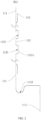
- FIG. 2 shows the side view of the cells contact sheet 011 according to one or more embodiments of the present application.
- the connecting sheet 112 includes a sheet body and a first bending structure 1121, and the first bending structure 1121 is convex to the cell groups from the location of the sheet body of the connecting sheet 112.
- the first bending structure 1121 is convex towards the cell group from the location of the sheet body of the connecting sheet 112, so that the cells contact sheet 011 can have a structure for buffering the pulling or squeezing of the cells contact sheet 011, and the first bending structure 1121 is overlapped with the busbar 131 on the axis of the cells, thus, avoiding the arranging of the first bending structure 1121 increases the height of the cells contact system 001, which is conducive to the layout of the electrical parts inside the battery pack.
- the first bending structure 1121 shown in FIG. 2 has a first surface 11211 located in the middle of the first bending structure 1121 and toward the cell groups.
- the first surface 11211 is parallel to the cells contact sub-sheet 111.
- the first bending structure 1121 is a U-shaped structure convex to the cell groups, where the side of the part facing the cell groups is the first surface 11211.
- the connecting sheet 112 includes two extension segments and a first bending structure 1121 located between the two extension segments.
- the two extension segments are respectively connected with two cells contact sub-sheets 111.
- the first bending structure 1121 includes a first bending segment, a second bending segment and a third bending segment successively connected.
- the first bending segment and the third bending segment are arranged relative to each other.
- the ends of the first bending segment and the third bending segment deviated from the second bending segment are connected to the two extension segments respectively.
- the first surface 11211 is on the side of the second bending segment facing the cell group.
- the first bending structure 1121 has a longer length in a certain space, so that the first bending structure 1121 has a larger buffer size, and then the first bending structure 1121 can achieve a better buffer effect in a limited space.
- the first signal output terminal 1111 is connected to the BMS board.
- the first signal output terminal 1111 is connected with the BMS board via a connector 063 to transmit the acquired work signals to the BMS board.
- the cells contact sub-sheet 111 closer to the BMS board is the output cells contact sub-sheet 111
- the end of the output cells contact sub-sheet 111 near the BMS board is the first signal output terminal 1111.
- the first signal output terminal 1111 Since the first signal output terminal 1111 is connected to the BMS board, the first signal output terminal 1111 is fixed. When the cells generate thermal expansion, it will pull on the joint between the first signal output terminal 1111 and the BMS board. Based on this, in the present embodiment, a second bending structure 1112 is provided at one end of the output cells contact sub-sheet 111 near the first signal output terminal 1111, so that the end of the output cells contact sub-sheet 111 near the first signal output terminal 1111 is provided with a structure for buffering the pulling of the first signal output terminal 1111 when the cell groups expand. Thus, the reliability of the connection between the cells contact sheet 011 and the BMS board is improved, and the cells contact sheet 011 is prevented from being torn.
- the second bending structure 1112 shown in FIG. 2 is an arc structure with concave surface away from the first signal output terminal 1111.
- the side of the second bending structure 1112 away from the first signal output terminal 1111 is tangent to the side of the cells contact sub-sheet 111 located at the second bending structure 1112 away from the first signal output terminal 1111.
- the stress of the second bending structure 1112 can be reduced, thereby improving the impact resistance of the cells contact sheet 011 and thereby improving the reliability of the cells contact sheet 011.
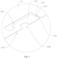
- FIG. 3 is an enlarged view of part A in FIG. 1 .
- the cells contact sub-sheet 111 has a voltage acquisition area 1113.
- the voltage acquisition area 1113 is provided with an acquisition notch 1114.
- An acquisition terminal sheet 1115 which is configured to acquire the voltage of the cell group is provided in the acquisition notch 1114.
- the acquisition terminal sheet 1115 has a first end and a second end opposite to each other, and the first end is connected with one surface of the acquisition notch 1114.
- the second end is connected with another surface of the acquisition notch 114. From the first end to the second end, there is a gap 1116 between the acquisition terminal sheet 1115 and the acquisition notch 1114.
- the cells contact sub-sheet 111 can acquire the voltage information of the cells; on the other hand, when the cells expands, the pulling force on the acquisition terminal sheet 1115 is mainly applicable to the first and second ends of the acquisition terminal sheet 1115, thus reducing the pulling force borne by the acquisition terminal sheet 1115, and then avoiding the weld between the acquisition terminal sheet 1115 and the busbar 131 falling off.
- the stability of the connection between the acquisition terminal sheet 1115 and the busbar 131 can be improved.
- connection structure by connecting the second end of the acquisition terminal sheet 1115 with the surface of the acquisition notch 1114 through the connection structure, when the acquisition terminal sheet 1115 bearing relatively large pulling force, the connection structure at one end of the acquisition terminal sheet 1115 can be disconnected through the pulling force to reduce the pulling force borne by the acquisition terminal sheet 1115.
- the weld between the acquisition terminal sheet 1115 and busbar 131 can be avoided from falling off, and the stability of the connection between the acquisition terminal sheet 1115 and busbar 131 can be improved.
- connection structure may adopt a structure thinner than the acquisition terminal sheet 1115, or a material with lower strength than the joint between the first end of the acquisition terminal sheet 1115 and the acquisition notch 1114.
- the connection structure includes a connection strip 1117.
- the two ends of the connection strip 1117 are respectively connected with the second end of the acquisition terminal sheet 1115 and a surface of the acquisition notch 1114.
- the middle part of the connection strip 1117 is provided with a cutting notch 11171.
- the cutting notch 11171 is configured to cause the connection strip 1117 to break when the cells contact sub-sheet 111 is pulled.
- the acquisition terminal sheet 1115 shown in FIG. 3 is provided with a buffer notch 11151.
- the buffer notch 11151 is arranged between the first end of the acquisition terminal sheet 1115 and the second end of the acquisition terminal sheet 1115.
- the stress of the acquisition terminal sheet 1115 during thermal expansion can be alleviated by arranging the buffer notch 11151, thereby improving the stability of the connection between the acquisition terminal sheet 1115 and the busbar 131.
- the edge of the cells contact sub-sheet 111 shown in FIG. 1 is connected with a bent terminal sheet 113 configured to acquire the temperature of the cell group.
- the deformability of the bent terminal sheet 113 can be used to buffer the pulling of the cells contact sheet 011 by the thermal expansion of the cells, thereby improving the load bearing capacity of the cells contact sheet 011, and thereby preventing the cells contact sheet 011 from being torn or the disconnection between the bent terminal sheet 113 and the cells contact sub-sheet 111.
- the reliability of the cells contact sheet 011 can be improved.
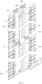
- FIG. 4 schematically shows the structure of the cells contact system 001 according to one or more embodiments of the present application.
- a cells contact system 001 is provided in embodiments of the present application.
- the cells contact system 001 includes a holder 012, busbar groups 013 and the aforementioned cells contact sheet 011.
- the busbar groups 013 include two busbar groups 013.
- the two busbar groups 013 are arranged successively on the holder 012.
- the two busbar groups 013 are configured to respectively connect with the two cell groups.
- Two cells contact sub-sheets 111 are connected to the two busbar groups 013 respectively.
- the connecting sheet 112 is located between the two adjacent busbar groups 013.
- first bending structures 1121 there are two first bending structures 1121 arranged at intervals along the arranging direction of the two cells contact sub-sheets 111.
- the first bending structure 1121 is convex from the position of the sheet body of the connecting sheet 112 towards the cell groups.
- the cells contact sub-sheet 111 is arranged on the holder 012.
- Groove 121 is provided on the holder 012.
- the two first bending structures 1121 are located in the two grooves 121 respectively, as shown in FIG. 5 , which is an enlarged view of part B in FIG. 4 .
- the first bending structure 1121 is fitted with gap 1116 of the groove 121.
- the gap 1116 between the first bending structure 1121 and the groove 121 is used to provide deformation space for a first bend of the first bending structure 1121, so that the deformation of the first bend of first bending structure 1121 is not hindered.
- the concave surface of the second bending structure 1112 faces the end face of the holder 012, as shown in FIF. 6, which is an enlarged view of part C in FIG. 4 .
- Two busbars 131 are connected with two cell groups 081 respectively.
- the two cells contact sub-sheets 111 one is the output cells contact sub-sheet 111.
- the first signal output terminal 1111 of the output cells contact sub-sheet 111 is connected to the BMS board. Specifically, the first signal output terminal 1111 is connected to the BMS board via connector 063.
Landscapes
- Chemical & Material Sciences (AREA)
- Chemical Kinetics & Catalysis (AREA)
- Electrochemistry (AREA)
- General Chemical & Material Sciences (AREA)
- Engineering & Computer Science (AREA)
- Manufacturing & Machinery (AREA)
- Microelectronics & Electronic Packaging (AREA)
- Battery Mounting, Suspending (AREA)
- Secondary Cells (AREA)
- Connection Of Batteries Or Terminals (AREA)
Abstract
Description
- The present application relates to battery technologies, in particular to cells contact sheets, cells contact systems and battery packs.
- Generally, a battery pack includes a housing, a battery module, a battery management system (BMS) board, and a cells contact system (CCS) that electrically connects the battery module with the BMS board. The battery module, the BMS board and the CCS are arranged in the housing. The CCS includes a busbar electrically connected to cells of the battery module and a cells contact sheet electrically connected to the busbar and the cells. The cells contact sheet is usually a flexible printed circuit board (FPCB). The cells contact sheet is used to transmit temperature signals and voltage signals of the cells to the BMS board through a harness and a connector in sequence.
- When the battery module includes multiple cell groups, in order to reduce the number of electrical parts and the difficulty of wiring, a cells contact sheet is usually used to acquire the temperature signals and voltage signals of the multiple cell groups. However, during the use of the battery module, a cell may expand due to rising temperature and thus produce tension on the cells contact sheet welded to the cell, so that the weld between the cells contact sheet and the cell may be broken and even the cells contact sheet may be torn. Therefore, the reliability of the acquisition result may be reduced.
- According to one or more embodiments of the present application, a cells contact sheet applicable to a battery module including a plurality of cell groups is provided. The cells contact sheet includes cells contact sub-sheets and at least one connecting sheet being flexible and electrically conductive, and are configured to acquire work signals of the plurality of cell groups, respectively; each of the at least one connecting sheet is arranged between every two adjacent ones of the cells contact sub-sheets to connect the every two adjacent ones of the cells contact sub-sheets to each other; and the each of the at least one connecting sheet is provided with a first bending structure configured to deform when two of the cell groups respectively corresponding to the every two adjacent ones of the cells contact sub-sheets move away from each other or close to each other.
- According to one or more embodiments of the present application, a cells contact system including a holder, multiple busbars, and aforementioned cells contact sheet is provided. The busbars are arranged successively in parallel on the holder, and are configured to be connected with the multiple cell groups, respectively; and multiple cells contact sub-sheets are opposite to and connected with the multiple busbars, respectively.
- According to one or more embodiments of the present application, a battery pack includes a housing, a battery module, a BMS board, and at least one of aforementioned cells contact system. The housing is provided with a first accommodating cavity and a second accommodating cavity arranged in a longitudinal direction; the battery module is arranged in the first accommodating cavity and includes multiple cell groups arranged in the longitudinal direction; the BMS board is arranged in the second accommodating cavity; and one of the cells contact sub-sheets is provided with a first signal output terminal connected to the BMS board.
- In order to more clearly illustrate the embodiments of the present disclosure or related art, the following figures will be described in the embodiments are briefly introduced. It is obvious that the drawings are merely some embodiments of the present disclosure, a person having ordinary skill in this field can obtain other figures according to these figures without paying the premise.
-
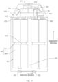
FIG. 1 schematically shows a structure of a cells contact sheet according to one or more embodiments of the present application. -
FIG. 2 is a side view of a cells contact sheet according to one or more embodiments of the present application. -
FIG. 3 is an enlarged view of part A inFIG. 1 . -
FIG. 4 schematically shows a structure of a cells contact system according to one or more embodiments of the present application. -
FIG. 5 is an enlarged view of part B inFIG. 4 . -
FIG. 6 is an enlarged view of part C inFIG. 4 . -
FIG. 7 is an enlarged view of part D inFIG. 4 . -
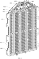
FIG. 8 schematically shows a structure of a battery pack according to one or more embodiments of the present application. -
FIG. 9 schematically shows wiring between a battery charge and discharge interface and a battery energy distribution unit (BDU) of a battery pack according to one or more embodiments of the present application. -
FIG. 10 schematically shows wiring of an acquisition harness of a battery pack according to one or more embodiments of the present application is a schematic diagram illustrating fallbackRAR according to an embodiment of the present disclosure. - Embodiments of the present disclosure are described in detail with the technical matters, structural features, achieved objects, and effects with reference to the accompanying drawings as follows. Specifically, the terminologies in the embodiments of the present disclosure are merely for describing the purpose of the certain embodiment, but not to limit the disclosure.
-
FIG. 1 schematically shows a structure of acells contact sheet 011 applicable to a battery module according to one or more embodiments of the present application. For example, the battery module includes two cell groups. Thecells contact sheet 011 includes two cells contactsub-sheets 111 and a flexibleconductive connecting sheet 112. The two cells contactsub-sheets 111 are arranged successively in parallel. The two cells contactsub-sheets 111 are configured respectively to acquire work signals of the two cell groups. The connectingsheet 112 is arranged between the two cells contactsub-sheets 111. The two ends of the connectingsheet 112 are respectively connected with the two cells contactsub-sheets 111, and the connectingsheet 112 is provided with afirst bending structure 1121, which is configured to deform when the two cell groups move away from or close to each other. - It can be understood that when the two cell groups move away from each other or close to each other, the
first bending structure 1121 will undergo flexible deformation due to the flexibility of the connectingsheet 112. When the connectingsheet 112 is an elastic metal sheet, thefirst bending structure 1121 also has an elastic deformation. Among them, the work signals are mainly voltage signals of the cells and temperature signals of the cell groups. - In addition, the cells contact
sub-sheet 111 has avoltage acquisition area 1113, thevoltage acquisition area 1113 is connected with abusbar 131, and thebusbar 131 is connected with the cell, so as to realize thecells contact sub-sheet 111 acquiring the voltage signal of the cell. The cell group includes a plurality of cells connected in series or in parallel through thebusbar 131. - Illustratively, the cells contact
sub-sheet 111 and the connectingsheet 112 are both flexible circuit boards, and thecells contact sheet 011 is an integrally-formed part. The flexible circuit board is a structure formed by etching aluminium foil or copper foil in one body to have a number of lines for transmitting electrical signals. - In the present embodiment, by arranging a
first bending structure 1121 at the part of thecells contact sheet 011 between the two cell groups, the cells contact sheet is provided with a buffer part formed based on thefirst bending structure 1121, in this way, when the cell groups produce thermal expansion, the buffer part can be deformed to buffer the expansion between the cell groups to pull thecells contact sheet 011, and then improve the stability of the welding part between the cells contact sheet 11 and the cells, and avoid thecells contact sheet 011 being torn, and finally improve the reliability of thecells contact sheet 011. - In addition, there are assembly tolerances between the cell groups and the
housing 002. Therefore, when assembling the cell groups to thehousing 002, thefirst bending structure 1121 can be squeezed or stretched to make the two cells contactsub-sheets 111 fit the assembly position of the cell groups, so as to improve the pulling or squeezing at the connection part between thecells contact sheet 011 and the cell groups due to assembly errors, and thus improve the reliability of the connection between thecells contact sheet 011 and the cell groups. -
FIG. 2 shows the side view of thecells contact sheet 011 according to one or more embodiments of the present application. In one or more embodiments, the connectingsheet 112 includes a sheet body and afirst bending structure 1121, and thefirst bending structure 1121 is convex to the cell groups from the location of the sheet body of the connectingsheet 112. - It can be understood that a
busbar 131 is arranged between thecells contact sheet 111 and the cells, and thevoltage acquisition area 1113 of thecells contact sheet 011 is welded with thebusbar 131 to acquire the voltage information of the cells. Thefirst bending structure 1121 is not used for acquiring voltage signals, so on the side of thebending structure 1121 facing the cell group is theholder 012. - Based on this, in the present embodiment, the
first bending structure 1121 is convex towards the cell group from the location of the sheet body of the connectingsheet 112, so that thecells contact sheet 011 can have a structure for buffering the pulling or squeezing of thecells contact sheet 011, and thefirst bending structure 1121 is overlapped with thebusbar 131 on the axis of the cells, thus, avoiding the arranging of thefirst bending structure 1121 increases the height of thecells contact system 001, which is conducive to the layout of the electrical parts inside the battery pack. - In one or more embodiments, the
first bending structure 1121 shown inFIG. 2 has afirst surface 11211 located in the middle of thefirst bending structure 1121 and toward the cell groups. Thefirst surface 11211 is parallel to the cells contactsub-sheet 111. - It can be understood that the
first bending structure 1121 is a U-shaped structure convex to the cell groups, where the side of the part facing the cell groups is thefirst surface 11211. In particular, the connectingsheet 112 includes two extension segments and afirst bending structure 1121 located between the two extension segments. The two extension segments are respectively connected with twocells contact sub-sheets 111. Thefirst bending structure 1121 includes a first bending segment, a second bending segment and a third bending segment successively connected. The first bending segment and the third bending segment are arranged relative to each other. The ends of the first bending segment and the third bending segment deviated from the second bending segment are connected to the two extension segments respectively. Thefirst surface 11211 is on the side of the second bending segment facing the cell group. - In the present embodiment, through the above arranging, the
first bending structure 1121 has a longer length in a certain space, so that thefirst bending structure 1121 has a larger buffer size, and then thefirst bending structure 1121 can achieve a better buffer effect in a limited space. - In one or more embodiments, the corners of the
first bending structure 1121 shown inFIG. 2 are rounded. - It is understood that the joint between one extension segment and the first bending segment, the joint between the first bending segment and the second bending segment, the joint between the second bending segment and the third bending segment, and the joint between the third bending segment and another extension segment are corners. Rounded corners are provided at each of the above joints. The rounded corners are formed by bending the connecting
sheet 112. - In the present embodiment, by providing a rounded corner at the corner of the
first bending structure 1121, the stress at the corner can be reduced, thereby improving the impact resistance of thecells contact sheet 011 and thereby improving the reliability of thecells contact sheet 011. - In one or more embodiments, one of the two cells contact
sub-sheets 111 shown inFIG. 2 is the outputcells contact sub-sheet 111. The output cells contact sub-sheet 111 has a firstsignal output terminal 1111. The output cells contact sub-sheet 111 is provided with asecond bending structure 1112, and thesecond bending structure 1112 is arranged near the firstsignal output terminal 1111. Thesecond bending structure 1112 is configured to deform when the firstsignal output terminal 1111 and the cell groups move away from or close to each other. - It is understood that the first
signal output terminal 1111 is connected to the BMS board. Generally, the firstsignal output terminal 1111 is connected with the BMS board via aconnector 063 to transmit the acquired work signals to the BMS board. In addition, among the twocells contact sub-sheets 111, the cells contact sub-sheet 111 closer to the BMS board is the output cells contact sub-sheet 111, and the end of the output cells contact sub-sheet 111 near the BMS board is the firstsignal output terminal 1111. - Since the first
signal output terminal 1111 is connected to the BMS board, the firstsignal output terminal 1111 is fixed. When the cells generate thermal expansion, it will pull on the joint between the firstsignal output terminal 1111 and the BMS board. Based on this, in the present embodiment, asecond bending structure 1112 is provided at one end of the output cells contact sub-sheet 111 near the firstsignal output terminal 1111, so that the end of the output cells contact sub-sheet 111 near the firstsignal output terminal 1111 is provided with a structure for buffering the pulling of the firstsignal output terminal 1111 when the cell groups expand. Thus, the reliability of the connection between thecells contact sheet 011 and the BMS board is improved, and thecells contact sheet 011 is prevented from being torn. - In one or more embodiments, the
second bending structure 1112 shown inFIG. 2 is an arc structure with concave surface away from the firstsignal output terminal 1111. - Illustratively, the side of the
second bending structure 1112 away from the firstsignal output terminal 1111 is tangent to the side of the cells contact sub-sheet 111 located at thesecond bending structure 1112 away from the firstsignal output terminal 1111. - In the present embodiment, by arranging the
second bending structure 1112 as an arc structure, the stress of thesecond bending structure 1112 can be reduced, thereby improving the impact resistance of thecells contact sheet 011 and thereby improving the reliability of thecells contact sheet 011. -
FIG. 3 is an enlarged view of part A inFIG. 1 . In one or more embodiments, thecells contact sub-sheet 111 has avoltage acquisition area 1113. Thevoltage acquisition area 1113 is provided with anacquisition notch 1114. Anacquisition terminal sheet 1115 which is configured to acquire the voltage of the cell group is provided in theacquisition notch 1114. Theacquisition terminal sheet 1115 has a first end and a second end opposite to each other, and the first end is connected with one surface of theacquisition notch 1114. The second end is connected with another surface of the acquisition notch 114. From the first end to the second end, there is agap 1116 between theacquisition terminal sheet 1115 and theacquisition notch 1114. - It can be understood that the
voltage acquisition area 1113 is the area on the cells contact sub-sheet 111 connected with thebusbar 131. Specifically, theacquisition terminal sheet 1115 is welded with thebusbar 131 to acquire the voltage information of the cell. - In the present embodiment, through the above arranging, on the one hand, the cells contact sub-sheet 111 can acquire the voltage information of the cells; on the other hand, when the cells expands, the pulling force on the
acquisition terminal sheet 1115 is mainly applicable to the first and second ends of theacquisition terminal sheet 1115, thus reducing the pulling force borne by theacquisition terminal sheet 1115, and then avoiding the weld between theacquisition terminal sheet 1115 and thebusbar 131 falling off. The stability of the connection between theacquisition terminal sheet 1115 and thebusbar 131 can be improved. - As shown in
FIG. 3 , in one or more embodiments, the second end of theacquisition terminal sheet 1115 is connected with another surface of theacquisition notch 1114 through a connection structure, and the connection structure is configured to break when thecells contact sub-sheet 111 is pulled. - It is understood that the pulling force of disconnecting the connection structure is less than that of disconnecting the connection between the
acquisition terminal sheet 1115 and thebusbar 131. In addition, the connecting structure fixed theacquisition terminal sheet 1115 in theacquisition notch 1114, which can avoid the second end of theacquisition terminal sheet 1115 falling down due to gravity and cause folding, so as to ensure the convenience of the assembly of the cells contact sheet. - In the present embodiment, by connecting the second end of the
acquisition terminal sheet 1115 with the surface of theacquisition notch 1114 through the connection structure, when theacquisition terminal sheet 1115 bearing relatively large pulling force, the connection structure at one end of theacquisition terminal sheet 1115 can be disconnected through the pulling force to reduce the pulling force borne by theacquisition terminal sheet 1115. Thus, the weld between theacquisition terminal sheet 1115 andbusbar 131 can be avoided from falling off, and the stability of the connection between theacquisition terminal sheet 1115 andbusbar 131 can be improved. - The connection structure may adopt a structure thinner than the
acquisition terminal sheet 1115, or a material with lower strength than the joint between the first end of theacquisition terminal sheet 1115 and theacquisition notch 1114. In particular, the connection structure includes aconnection strip 1117. The two ends of theconnection strip 1117 are respectively connected with the second end of theacquisition terminal sheet 1115 and a surface of theacquisition notch 1114. The middle part of theconnection strip 1117 is provided with a cuttingnotch 11171. The cuttingnotch 11171 is configured to cause theconnection strip 1117 to break when thecells contact sub-sheet 111 is pulled. - In one or more embodiments, the
acquisition terminal sheet 1115 shown inFIG. 3 is provided with abuffer notch 11151. Thebuffer notch 11151 is arranged between the first end of theacquisition terminal sheet 1115 and the second end of theacquisition terminal sheet 1115. - In the present embodiment, the stress of the
acquisition terminal sheet 1115 during thermal expansion can be alleviated by arranging thebuffer notch 11151, thereby improving the stability of the connection between theacquisition terminal sheet 1115 and thebusbar 131. - In one or more embodiments, the edge of the cells contact sub-sheet 111 shown in
FIG. 1 is connected with abent terminal sheet 113 configured to acquire the temperature of the cell group. - It is understood that the
bent terminal sheet 113 is located at the outer edge of thecells contact sub-sheet 111 and formed in one piece with thecells contact sub-sheet 111. - In the present embodiment, by using the
bent terminal sheet 113 to acquire the temperature information of the cell group, the deformability of thebent terminal sheet 113 can be used to buffer the pulling of thecells contact sheet 011 by the thermal expansion of the cells, thereby improving the load bearing capacity of thecells contact sheet 011, and thereby preventing thecells contact sheet 011 from being torn or the disconnection between thebent terminal sheet 113 and thecells contact sub-sheet 111. Thus, the reliability of thecells contact sheet 011 can be improved. -
FIG. 4 schematically shows the structure of thecells contact system 001 according to one or more embodiments of the present application. Accordingly, acells contact system 001 is provided in embodiments of the present application. Thecells contact system 001 includes aholder 012,busbar groups 013 and the aforementionedcells contact sheet 011. Thebusbar groups 013 include twobusbar groups 013. The twobusbar groups 013 are arranged successively on theholder 012. The twobusbar groups 013 are configured to respectively connect with the two cell groups. Two cells contact sub-sheets 111 are connected to the twobusbar groups 013 respectively. The connectingsheet 112 is located between the twoadjacent busbar groups 013. - Illustratively, there are two
first bending structures 1121 arranged at intervals along the arranging direction of the twocells contact sub-sheets 111. Thefirst bending structure 1121 is convex from the position of the sheet body of the connectingsheet 112 towards the cell groups. The cells contact sub-sheet 111 is arranged on theholder 012.Groove 121 is provided on theholder 012. There are twogrooves 121. The twofirst bending structures 1121 are located in the twogrooves 121 respectively, as shown inFIG. 5 , which is an enlarged view of part B inFIG. 4 . Thefirst bending structure 1121 is fitted withgap 1116 of thegroove 121. Thegap 1116 between thefirst bending structure 1121 and thegroove 121 is used to provide deformation space for a first bend of thefirst bending structure 1121, so that the deformation of the first bend offirst bending structure 1121 is not hindered. - In addition, the concave surface of the
second bending structure 1112 faces the end face of theholder 012, as shown in FIF. 6, which is an enlarged view of part C inFIG. 4 . - Among them, the
holder 012 is a blister holder.Busbar groups 013 include a plurality ofbusbars 131, which is used to parallel two adjacent cells. Accordingly, a plurality ofvoltage acquisition areas 1113 are arranged on the cells contactsub-sheets 111, and the plurality ofvoltage acquisition areas 1113 are respectively connected with the plurality ofbusbars 131.Busbar 131 is an O-state aluminium bar.Busbar 131 is welded to the pole of the cell. The connection structure between thebusbar 131 and cells contact sub-sheet 111 is shown inFIG. 7 , which is an enlarged view of part D inFIG. 4 . Thevoltage acquisition area 1113 of thecells contact sub-sheet 111 is connected to thebusbar 131 through theconductive sheet 132. In particular, one end of theconductive sheet 132 is welded to the part of theacquisition terminal sheet 1115 between thebuffer notch 11151 and the second end of theacquisition terminal sheet 1115, and the other end is welded to the end of thebusbar 131 near thecells contact sub-sheet 111. - In the present embodiment, by adopting the aforementioned
cells contact sheet 011, thefirst bending structure 1121 can be used to generate deformation during thermal expansion of the cell groups to buffer the pull of the expansion between the cell groups on thecells contact sheet 011, thereby improving the stability of the welding part between thecells contact sheet 011 and the cells, and avoiding the tearing of thecells contact sheet 011, finally improving the reliability of thecells contact system 001. -
FIG. 8 schematically shows a structure of a battery pack according to one or more embodiments of the present application (the cover ofhousing 002 is hidden inFIG. 8 for ease of showing the internal structure of the housing). Accordingly, one or more embodiments of the present application further provide a battery pack including ahousing 002, abattery module 008, a BMS board and the aforementionedcells contact system 001. Thehousing 002 has a firstaccommodating cavity 021 and a secondaccommodating cavity 022 arranged in a longitudinal direction. Thebattery module 008 is arranged in the firstaccommodating cavity 021. Thebattery module 008 includes twocell groups 081 arranged in the longitudinal direction. The BMS board is arranged in the secondaccommodating cavity 022. Thecells contact system 001 is arranged in the firstaccommodating cavity 021. Twobusbars 131 are connected with twocell groups 081 respectively. Among the twocells contact sub-sheets 111, one is the outputcells contact sub-sheet 111. The firstsignal output terminal 1111 of the output cells contact sub-sheet 111 is connected to the BMS board. Specifically, the firstsignal output terminal 1111 is connected to the BMS board viaconnector 063. - Illustratively, the first
accommodating cavity 021 and the secondaccommodating cavity 022 are formed by separating the inner cavity of the battery pack between via anend partition 025. In addition, across beam 023 is arranged in the firstaccommodating cavity 021. Thecross beam 023 is connected with the cavity wall of the firstaccommodating cavity 021. Thecross beam 023 is located between the twocell groups 081 ofbattery module 008 to separate the twocell groups 081. - In the present embodiment, by adopting the
cells contact system 001 mentioned above, during thermal expansion ofcell groups 081, the deformation of thefirst bending structure 1121 can be generated to buffer the pull of the expansion betweencell groups 081 on thecells contact sheet 011, thereby improving the stability of the welding part between thecells contact sheet 011 and the cells, and avoiding the tearing of thecells contact sheet 011, finally improving the reliability of the battery pack. - As shown in
FIG. 8 , in one or more embodiments, there are fourbattery modules 008 and fourcells contact systems 001. The fourbattery modules 008 are arranged along a transverse direction in the firstaccommodating cavity 021. The transverse direction is perpendicular to the longitudinal direction. The fourbattery modules 008 and the fourcells contact systems 001 are arranged according to a one-to-one correspondence. In order to improve the assembling stability ofbattery modules 008, alongitudinal beam 024 is arranged between twoadjacent battery modules 008, and thelongitudinal beam 024 is connected with the inner wall ofhousing 002. - It can be understood that there are eight
cell groups 081 corresponding to fourbattery modules 008. The eightcell groups 081 are connected in series through O-state aluminium bars. - As shown in
FIG. 8 , in one or more embodiments, the battery pack further includes a battery energy distribution device (for example, a battery energy distribution unit (BDU)), a battery charge and discharge interface, and a charge and discharge connection bar. The BDU is arranged in the secondaccommodating cavity 022, the battery charge and discharge interface is arranged on the side of thehousing 002 away from the secondaccommodating cavity 022, two ends of the charge and discharge connection bar are connected with the BDU and the battery charge and discharge interface respectively, and the charge and discharge connection bar is arranged on the end of thelongitudinal beam 024 away from the inner wall of thehousing 002. - Illustratively, the charge and discharge connection bar includes a middle bar and end bars, and the end bars include two end bars, an end bar connects the end of the middle bar with the BDU, and the other end bar connects the other end of the middle bar with the battery charge and discharge interface, and the end bars are soft metal bars. The middle bar is a 6-series aluminium bar, and the end bars are specifically copper bars. The end bars and the middle bar are welded together by polymer diffusion welding. The soft copper bar can be deformed during assembling to effectively absorb assembly tolerances, thus improving the convenience of connecting the charge and discharge connection bar to the BDU and the battery charge and discharge interface. At the same time, the soft copper bar can better absorb the pulling force caused by the vibration of the vehicle during driving, and avoid disconnection of the high voltage circuit or leakage due to the tension of the charge and discharge connection bar.
- In addition, the battery pack is also equipped with a
fast charge interface 071. Thefast charge interface 071 is located on the side of the battery pack near the BDU. - In the conventional assembling mode, the charge and discharge connection bar is arranged on the wall of the
housing 002. The charge and discharge connection bar needs to retain a safe distance from thebusbar 131 and the cells, so the first inner cavity needs to have enough space in the longitudinal direction to meet requirements of the installation of relevant parts, and also needs to meet requirements of the safety spacing between the aforementioned parts. - Based on this, in the present embodiment, the charge and discharge connection bar is arranged on the
longitudinal beam 024. On the one hand, the space occupied by thelongitudinal beam 024 can be utilized, so that the required installation space of the charge and discharge connection bar can be overlapped with the space of thelongitudinal beam 024, and the utilization rate of the internal space of the battery pack can be improved. Thus, the original space for arranging the charge and discharge connection bar can be used to increase the transverse size of the cells, so as to improve the energy density of the battery pack. On the other hand, the charge and discharge connection bar is set on thelongitudinal beam 024, which can avoid the outer wall of the battery pack being squeezed and cause the insulation layer of the charge and discharge connection bar to break, so as to improve the reliability of the battery pack. -
FIG. 9 schematically shows wiring between a battery charge and discharge interface and a BDU of a battery pack according to one or more embodiments of the present application. In one or more embodiments, the battery charge and discharge interface includescharge interface 051 and dischargeinterface 052. The charge and discharge connection bar includes a chargepositive bar 041, a dischargepositive bar 042 and a charge and dischargenegative bar 043. The positive port ofcharge interface 051 is connected to thepositive port 031 of the BDU through chargepositive bar 041. The positive port of thedischarge interface 052 is connected to thepositive port 031 of the BDU via the dischargepositive bar 042. One end of the charge and dischargenegative bar 043 is connected to the negative port of thecharge interface 051 and the negative port of thedischarge interface 052, and the other end is connected to thenegative port 032 of the BDU. - In
FIG. 9 , from left to right, the three long solid lines in the middle are the chargepositive bar 041, the charge and dischargenegative bar 043, and the dischargepositive bar 042 in sequence. -
FIG. 10 schematically shows wiring of harnesses for part of acquisition signals of a battery pack according to one or more embodiments of the present application. The BMS board includes the BMSmain board 061 and threeBMS slave boards 062. - It is understood that the battery pack includes four
battery modules 008. And eachbattery module 008 includes twocell groups 081. The twobattery modules 081 include of 25 cells and 26 cells respectively. Therefore, the signal source is too many, and only one BMSmain board 061 is not conducive to data processing. Based on this, the BMS board is set as one BMSmain board 061 and threeBMS slave board 062, which can improve the data processing efficiency, and then improve the reliability of the signal acquisition of the battery pack. Specifically, theBMS slave board 062 transforms the analog signals from thecells contact sheet 011 into a digital signal, and transmits the digital signals to the BMSmain board 061 through the daisy chain, and the BMSmain board 061 is connected to the control system of the vehicle through thecommunication interface 072. - While the present disclosure has been described in connection with what is considered the most practical and preferred embodiments, it is understood that the present disclosure is not limited to the disclosed embodiments but is intended to cover various arrangements made without departing from the scope of the broadest interpretation of the appended claims.
Claims (15)
- A cells contact sheet (011), applicable to a battery module comprising a plurality of cell groups, characterized in that the cells contact sheet (011) comprises:a plurality of cells contact sub-sheets (111) configured to acquire work signals of the plurality of cell groups, respectively; andat least one connecting sheet (112) being flexible and electrically conductive,wherein each of the at least one connecting sheet (112) is arranged between every two adjacent ones of the cells contact sub-sheets (111) to connect the every two adjacent ones of the cells contact sub-sheets (111) to each other; andthe each of the at least one connecting sheet (112) is provided with a first bending structure (1121) configured to deform when two of the cell groups respectively corresponding to the every two adjacent ones of the cells contact sub-sheets (111) move away from each other or close to each other.
- The cells contact sheet of claim 1, characterized in that the each of the at least one connecting sheet further comprises a sheet body, and the first bending structure protrudes, relatively to the sheet body, toward the two of the cell groups.
- The cells contact sheet of claim 2, characterized in that the first bending structure has a first surface (11211), and the first surface (11211) is in a middle of the first bending structure and faces the two of the cell groups; and
the first surface (11211) is parallel to each of the cells contact sub-sheets. - The cells contact sheet of claim 3, characterized in that each corner of the first bending structure is rounded.
- The cells contact sheet of any one of claims 1-4, characterized in that one of the cells contact sub-sheets is provided with a first signal output terminal (1111) and a second bending structure (1112) close to the first signal output terminal (1111); and
the second bending structure (1112) is configured to deform when the first signal output terminal (1111) and two of the cell groups corresponding to the one of the cells contact sub-sheets move away from each other or close to each other. - The cells contact sheet of claim 5, characterized in that the second bending structure comprises an arc-shaped structure having a concave side away from the first signal output terminal.
- The cells contact sheet of any one of claims 1-4, characterized in that each of the cells contact sub-sheets has a voltage acquisition area (1113) comprising an acquisition notch (1114);an acquisition terminal sheet (1115) is arranged in the acquisition notch (1114) to acquire a voltage signal of one of the cell groups corresponding to the each of the cells contact sub-sheets;the acquisition terminal sheet (1115) has a first end connected with a first side surface of the acquisition notch (1114), and a second end being opposite to the first end and connected with a second side surface of the acquisition notch (1114); anda gap (1116) extending in a direction from the first end to the second end is formed between the acquisition terminal sheet (1115) and the acquisition notch (1114).
- The cells contact sheet of claim 7, characterized in that the second end of the acquisition terminal sheet is connected with the second side surface of the acquisition notch through a connection structure, and the connection structure is configured to break when the each of the cells contact sub-sheets is pulled.
- The cells contact sheet of claim 8, characterized in that the connection structure comprise a connection strip (1117) having two ends respectively connected with the second end of the acquisition terminal sheet and the second side surface of the acquisition notch; and
a cutting notch (11171) is provided in a middle of the connection strip (1117) and configured to cause the connection strip (1117) to break when the each of the cells contact sub-sheets is pulled. - The cells contact sheet of claim 7, characterized in that the acquisition terminal sheet is provided with a buffer notch (11151) between the first end and the second end.
- The cells contact sheet of any one of claims 1-4, characterized in that each of the cells contact sub-sheets has an edge connected with a bent terminal sheet (113) configured to acquire a temperature signal of one of the cell groups corresponding to the each of the cells contact sub-sheets.
- A cells contact system (001), characterized by comprising:a holder (012);a plurality of busbars (013) arranged in parallel on the holder (012) and configured to be respectively connected with a plurality of cell groups of a battery module; anda cells contact sheet of any one of claims 1-11,wherein the plurality of cells contact sub-sheets are opposite to and connected with the plurality of busbars (013), respectively.
- A battery pack, characterized by comprising:a housing (002) having a first accommodating cavity (021) and a second accommodating cavity (022) arranged in a longitudinal direction;at least one battery module (008) arranged in the first accommodating cavity (021), the battery module (008) comprising a plurality of cell groups (081) arranged in the longitudinal direction;a battery management system board arranged in the second accommodating cavity (022); andat least one cells contact system of claim 12 arranged in the first accommodating cavity (021),wherein one of the cells contact sub-sheets is provided with a first signal output terminal connected to the battery management system board.
- The battery pack of claim 13, characterized in that the at least one battery module comprises a plurality of battery modules, and the at least one cells contact system comprises a plurality of cells contact systems respectively corresponding to the plurality of battery modules; and
the plurality of battery modules are sequentially arranged in a transverse direction perpendicular to the longitudinal direction. - The battery pack of claim 14, characterized in that a longitudinal beam (024) is arranged between every two adjacent ones of the plurality of battery modules and connected to an inner wall of the housing.
Applications Claiming Priority (2)
| Application Number | Priority Date | Filing Date | Title |
|---|---|---|---|
| CN202323671458.3U CN222126930U (en) | 2023-12-31 | 2023-12-31 | Collecting sheet, collecting assembly and battery pack |
| PCT/CN2024/084037 WO2025138468A1 (en) | 2023-12-31 | 2024-03-27 | Cells contact piece, cells contact system and battery pack |
Publications (1)
| Publication Number | Publication Date |
|---|---|
| EP4583296A1 true EP4583296A1 (en) | 2025-07-09 |
Family
ID=93924445
Family Applications (1)
| Application Number | Title | Priority Date | Filing Date |
|---|---|---|---|
| EP24220032.7A Pending EP4583296A1 (en) | 2023-12-31 | 2024-12-16 | Cells contact sheets, cells contact systems, and battery packs |
Country Status (3)
| Country | Link |
|---|---|
| US (1) | US20250219167A1 (en) |
| EP (1) | EP4583296A1 (en) |
| DE (1) | DE202024107163U1 (en) |
Citations (4)
| Publication number | Priority date | Publication date | Assignee | Title |
|---|---|---|---|---|
| US20120328920A1 (en) * | 2010-03-12 | 2012-12-27 | Autonetworks Technologies, Ltd. | Battery module |
| DE102019134469A1 (en) * | 2018-12-29 | 2020-07-02 | Molex, Llc | Battery connection module |
| US20220255141A1 (en) * | 2021-02-09 | 2022-08-11 | Molex, Llc | Battery connection module |
| EP4195371A2 (en) * | 2021-12-13 | 2023-06-14 | Hyundai Motor Company | Battery pack for vehicle |
-
2024
- 2024-12-10 DE DE202024107163.8U patent/DE202024107163U1/en active Active
- 2024-12-16 EP EP24220032.7A patent/EP4583296A1/en active Pending
- 2024-12-22 US US18/991,644 patent/US20250219167A1/en active Pending
Patent Citations (4)
| Publication number | Priority date | Publication date | Assignee | Title |
|---|---|---|---|---|
| US20120328920A1 (en) * | 2010-03-12 | 2012-12-27 | Autonetworks Technologies, Ltd. | Battery module |
| DE102019134469A1 (en) * | 2018-12-29 | 2020-07-02 | Molex, Llc | Battery connection module |
| US20220255141A1 (en) * | 2021-02-09 | 2022-08-11 | Molex, Llc | Battery connection module |
| EP4195371A2 (en) * | 2021-12-13 | 2023-06-14 | Hyundai Motor Company | Battery pack for vehicle |
Also Published As
| Publication number | Publication date |
|---|---|
| US20250219167A1 (en) | 2025-07-03 |
| DE202024107163U1 (en) | 2024-12-23 |
Similar Documents
| Publication | Publication Date | Title |
|---|---|---|
| KR102595362B1 (en) | Battery packs and vehicles | |
| US12148900B2 (en) | Sampling component, battery module, battery pack, and device | |
| CN112470335B (en) | Battery module and battery pack including the same | |
| EP3907818A1 (en) | Battery pack having movable busbar assembly, and secondary battery comprising same | |
| WO2020171629A1 (en) | Battery module including terminal connecting structure provided with floating nut and battery pack including the same | |
| WO2019151716A1 (en) | Battery module, and battery pack and automobile comprising same | |
| EP4064417B1 (en) | Battery module in which connection between electrode lead and voltage sensing member is simplified, and battery pack including the same | |
| EP4071888B1 (en) | Battery module in which connection between electrode lead and voltage sensing member is simplified, and battery pack including the same | |
| WO2020171627A1 (en) | Battery module including protective cover for covering flexible printed circuit board | |
| US12113241B2 (en) | Battery module | |
| CN222126930U (en) | Collecting sheet, collecting assembly and battery pack | |
| EP4583296A1 (en) | Cells contact sheets, cells contact systems, and battery packs | |
| CN218101500U (en) | Battery module structure | |
| EP3926745B1 (en) | Battery module | |
| CN115911720A (en) | Battery pack and vehicle | |
| US20240304933A1 (en) | Battery module | |
| CN223427702U (en) | Battery devices and power-consuming devices | |
| CN223598965U (en) | Battery pack and electric equipment | |
| EP4687191A1 (en) | Acquisition assembly, battery module, and battery box | |
| US20250141056A1 (en) | Battery module and manufacturing method thereof, battery pack, and electric device | |
| US20260024929A1 (en) | Multilayered flexible flat cable and manufacturing method thereof | |
| CN221057625U (en) | Sampling structure, battery module and battery pack | |
| CN121035536B (en) | Battery devices and electrical appliances | |
| CN217656026U (en) | Battery packs and powerplants | |
| CN218827708U (en) | FFC collection system, busbar composite set, battery module and battery package |
Legal Events
| Date | Code | Title | Description |
|---|---|---|---|
| PUAI | Public reference made under article 153(3) epc to a published international application that has entered the european phase |
Free format text: ORIGINAL CODE: 0009012 |
|
| STAA | Information on the status of an ep patent application or granted ep patent |
Free format text: STATUS: REQUEST FOR EXAMINATION WAS MADE |
|
| 17P | Request for examination filed |
Effective date: 20241216 |
|
| AK | Designated contracting states |
Kind code of ref document: A1 Designated state(s): AL AT BE BG CH CY CZ DE DK EE ES FI FR GB GR HR HU IE IS IT LI LT LU LV MC ME MK MT NL NO PL PT RO RS SE SI SK SM TR |
|
| GRAP | Despatch of communication of intention to grant a patent |
Free format text: ORIGINAL CODE: EPIDOSNIGR1 |
|
| STAA | Information on the status of an ep patent application or granted ep patent |
Free format text: STATUS: GRANT OF PATENT IS INTENDED |
|
| INTG | Intention to grant announced |
Effective date: 20260126 |
|
| GRAS | Grant fee paid |
Free format text: ORIGINAL CODE: EPIDOSNIGR3 |
|
| GRAA | (expected) grant |
Free format text: ORIGINAL CODE: 0009210 |
|
| STAA | Information on the status of an ep patent application or granted ep patent |
Free format text: STATUS: THE PATENT HAS BEEN GRANTED |