EP4583189A1 - Negative electrode and battery - Google Patents
Negative electrode and battery Download PDFInfo
- Publication number
- EP4583189A1 EP4583189A1 EP23860371.6A EP23860371A EP4583189A1 EP 4583189 A1 EP4583189 A1 EP 4583189A1 EP 23860371 A EP23860371 A EP 23860371A EP 4583189 A1 EP4583189 A1 EP 4583189A1
- Authority
- EP
- European Patent Office
- Prior art keywords
- negative electrode
- active material
- material layer
- layer
- positive electrode
- Prior art date
- Legal status (The legal status is an assumption and is not a legal conclusion. Google has not performed a legal analysis and makes no representation as to the accuracy of the status listed.)
- Pending
Links
Images




Classifications
-
- H—ELECTRICITY
- H01—ELECTRIC ELEMENTS
- H01M—PROCESSES OR MEANS, e.g. BATTERIES, FOR THE DIRECT CONVERSION OF CHEMICAL ENERGY INTO ELECTRICAL ENERGY
- H01M4/00—Electrodes
- H01M4/02—Electrodes composed of, or comprising, active material
- H01M4/13—Electrodes for accumulators with non-aqueous electrolyte, e.g. for lithium-accumulators; Processes of manufacture thereof
- H01M4/134—Electrodes based on metals, Si or alloys
-
- H—ELECTRICITY
- H01—ELECTRIC ELEMENTS
- H01M—PROCESSES OR MEANS, e.g. BATTERIES, FOR THE DIRECT CONVERSION OF CHEMICAL ENERGY INTO ELECTRICAL ENERGY
- H01M10/00—Secondary cells; Manufacture thereof
- H01M10/05—Accumulators with non-aqueous electrolyte
- H01M10/052—Li-accumulators
- H01M10/0525—Rocking-chair batteries, i.e. batteries with lithium insertion or intercalation in both electrodes; Lithium-ion batteries
-
- H—ELECTRICITY
- H01—ELECTRIC ELEMENTS
- H01M—PROCESSES OR MEANS, e.g. BATTERIES, FOR THE DIRECT CONVERSION OF CHEMICAL ENERGY INTO ELECTRICAL ENERGY
- H01M4/00—Electrodes
- H01M4/02—Electrodes composed of, or comprising, active material
- H01M4/36—Selection of substances as active materials, active masses, active liquids
- H01M4/362—Composites
- H01M4/364—Composites as mixtures
-
- H—ELECTRICITY
- H01—ELECTRIC ELEMENTS
- H01M—PROCESSES OR MEANS, e.g. BATTERIES, FOR THE DIRECT CONVERSION OF CHEMICAL ENERGY INTO ELECTRICAL ENERGY
- H01M4/00—Electrodes
- H01M4/02—Electrodes composed of, or comprising, active material
- H01M4/36—Selection of substances as active materials, active masses, active liquids
- H01M4/362—Composites
- H01M4/366—Composites as layered products
-
- H—ELECTRICITY
- H01—ELECTRIC ELEMENTS
- H01M—PROCESSES OR MEANS, e.g. BATTERIES, FOR THE DIRECT CONVERSION OF CHEMICAL ENERGY INTO ELECTRICAL ENERGY
- H01M4/00—Electrodes
- H01M4/02—Electrodes composed of, or comprising, active material
- H01M4/36—Selection of substances as active materials, active masses, active liquids
- H01M4/38—Selection of substances as active materials, active masses, active liquids of elements or alloys
- H01M4/386—Silicon or alloys based on silicon
-
- H—ELECTRICITY
- H01—ELECTRIC ELEMENTS
- H01M—PROCESSES OR MEANS, e.g. BATTERIES, FOR THE DIRECT CONVERSION OF CHEMICAL ENERGY INTO ELECTRICAL ENERGY
- H01M4/00—Electrodes
- H01M4/02—Electrodes composed of, or comprising, active material
- H01M4/36—Selection of substances as active materials, active masses, active liquids
- H01M4/58—Selection of substances as active materials, active masses, active liquids of inorganic compounds other than oxides or hydroxides, e.g. sulfides, selenides, tellurides, halogenides or LiCoFy; of polyanionic structures, e.g. phosphates, silicates or borates
- H01M4/583—Carbonaceous material, e.g. graphite-intercalation compounds or CFx
- H01M4/587—Carbonaceous material, e.g. graphite-intercalation compounds or CFx for inserting or intercalating light metals
-
- H—ELECTRICITY
- H01—ELECTRIC ELEMENTS
- H01M—PROCESSES OR MEANS, e.g. BATTERIES, FOR THE DIRECT CONVERSION OF CHEMICAL ENERGY INTO ELECTRICAL ENERGY
- H01M4/00—Electrodes
- H01M4/02—Electrodes composed of, or comprising, active material
- H01M4/62—Selection of inactive substances as ingredients for active masses, e.g. binders, fillers
- H01M4/621—Binders
- H01M4/622—Binders being polymers
-
- H—ELECTRICITY
- H01—ELECTRIC ELEMENTS
- H01M—PROCESSES OR MEANS, e.g. BATTERIES, FOR THE DIRECT CONVERSION OF CHEMICAL ENERGY INTO ELECTRICAL ENERGY
- H01M4/00—Electrodes
- H01M4/02—Electrodes composed of, or comprising, active material
- H01M2004/021—Physical characteristics, e.g. porosity, surface area
-
- H—ELECTRICITY
- H01—ELECTRIC ELEMENTS
- H01M—PROCESSES OR MEANS, e.g. BATTERIES, FOR THE DIRECT CONVERSION OF CHEMICAL ENERGY INTO ELECTRICAL ENERGY
- H01M4/00—Electrodes
- H01M4/02—Electrodes composed of, or comprising, active material
- H01M2004/026—Electrodes composed of, or comprising, active material characterised by the polarity
- H01M2004/027—Negative electrodes
-
- Y—GENERAL TAGGING OF NEW TECHNOLOGICAL DEVELOPMENTS; GENERAL TAGGING OF CROSS-SECTIONAL TECHNOLOGIES SPANNING OVER SEVERAL SECTIONS OF THE IPC; TECHNICAL SUBJECTS COVERED BY FORMER USPC CROSS-REFERENCE ART COLLECTIONS [XRACs] AND DIGESTS
- Y02—TECHNOLOGIES OR APPLICATIONS FOR MITIGATION OR ADAPTATION AGAINST CLIMATE CHANGE
- Y02E—REDUCTION OF GREENHOUSE GAS [GHG] EMISSIONS, RELATED TO ENERGY GENERATION, TRANSMISSION OR DISTRIBUTION
- Y02E60/00—Enabling technologies; Technologies with a potential or indirect contribution to GHG emissions mitigation
- Y02E60/10—Energy storage using batteries
Definitions
- the present disclosure relates to a negative electrode and a battery.
- Patent Literatures 1 to 6 Conventionally, a battery having a negative electrode including a plurality of active material layers has been known (see, for example, Patent Literatures 1 to 6).
- the negative electrode of the present disclosure includes a current collector layer, a first active material layer bonded to the current collector layer, and a second active material layer bonded to the first active material layer.
- the first active material layer includes a first graphite and a first silicon simple substance or silicon compound of 1 wt% or more and 90 wt% or less with respect to the total weight of the first active material layer.
- the second active material layer includes a second graphite having an average particle diameter smaller than that of the first graphite, and a second silicon simple substance or silicon compound having an average particle diameter of 0 wt% or more and less than 1 wt% with respect to the total weight of the second active material layer.
- a battery of the present disclosure includes the negative electrode, a positive electrode, and an electrolyte.
- the durability of the battery is improved.
- a lateral width direction X (X-axis direction), a depth direction Y (Y-axis direction), and a height direction Z (Z-axis direction) of the constituent members of the battery 1 and the battery 1 are indicated by arrows.
- the lateral width direction X, the depth direction Y, and the height direction Z indicate relative direction relationships.
- the battery 1 is rotated by 180 degrees and the upper surface and the lower surface are reversely rotated, or in a case where the battery 1 is rotated by 90 degrees and the upper surface is arranged as a side surface, the lateral width direction X, the depth direction Y, and the height direction Z of the battery 1 change.
- the positive electrode current collector layer 111 is formed in an elongated shape extending in the lateral width direction X. As illustrated in Figures 3 and 4 , the positive electrode current collector 111 includes a current collector 111a and a positive electrode tab 111b. The current collector 111a is long in the lateral width direction X and is formed in a foil shape. As shown in Figure 4 , the positive electrode active material layer 112 is bonded to the current collector 111a. The positive electrode active material layer 112 may be formed on both surfaces of the current collector 111a. For example, the positive electrode active material layer 112 faces all regions along a shorter direction (height direction Z) of the current collector 111a.
- the positive electrode active material layer 112 includes a positive electrode active material composed of a lithium-containing composite oxide, a binder, and a conductive auxiliary agent.
- lithium-containing composite oxide examples include metallic elements such as nickel (Nickel), cobalt (Cobalt), and manganese (Manganese), and lithium (Lithium).
- Examples of the lithium-containing composite oxide may be a ternary lithium-containing composite oxide represented by the following formula: Li 1+X M A O 2 (1) (wherein X satisfies -0.15 ⁇ X ⁇ 0.15, and M A represents an element group containing at least one selected from the group consisting of Mn and Al, Ni, and Co.)
- the ternary lithium-containing composite oxide represented by the above general composition formula (1) has a high thermal stability and a stability in a high potential state, and the safety of the battery 1 and various battery characteristics can be enhanced by applying the oxide.
- binder for example, polyvinylidene fluoride (PVdF), polytetrafluoroethylene (PTFE), polyethylene, polystyrene, polybutadiene, polyacrylonitrile, polyvinyl fluoride, polypropylene fluoride, polychloroprene fluoride, butyl rubber, nitrile rubber, styrene butadiene rubber (SBR), polysulfide rubber, nitrocellulose, cyanoethyl cellulose, various latexes, acrylic resins, or mixtures thereof can be used.
- PVdF polyvinylidene fluoride
- PTFE polytetrafluoroethylene
- SBR styrene butadiene rubber
- SBR styrene butadiene rubber
- a carbon-based material can be used as the conductive agent.
- the carbon-based material may be crystalline carbon, amorphous carbon, or mixtures thereof.
- the crystalline carbon include artificial graphite, natural graphite (e.g., scaly graphite), or mixtures thereof.
- the amorphous carbon include carbon black (e.g., acetylene black, Ketjen black, channel black, furnace black, lamp black, thermal black, or mixtures thereof).
- the positive electrode 110 can be formed, for example, as follows.
- the positive electrode active material and, optionally, the binder and the conductive agent are dispersed in a solvent (e.g., N-methyl-2-pyrrolidone (NMP), water) to prepare a paste-like or slurry-like positive electrode mixture composition.
- the positive electrode mixture composition is applied to the surface (one side or both sides) of the positive electrode current collector layer 111, dried, and subjected to calendering if necessary to form a positive electrode mixture layer.
- the positive electrode 110 is not limited to the one manufactured by the above-described manufacturing method, and may be manufactured by another method.
- the negative electrode 120 includes a negative electrode current collector layer 121, a negative electrode first active material layer 122 (first active material layer) bonded to the negative electrode current collector layer 121, and a negative electrode second active material layer 123 (second active material layer) bonded to the negative electrode first active material layer 122. That is, the negative electrode 120 includes a plurality of active material layers.
- the negative electrode current collector layer 121 is formed in an elongated shape extending in the lateral width direction X. As illustrated in Figures 3 and 4 , the negative electrode current collector 121 includes a current collector 121a and a negative electrode tab 121b. The current collector 121a is long in the lateral width direction X and is formed in a foil shape. As shown in Figure 4 , the current collector 121a has a longer width along the shorter direction (height direction Z) than the current collector 111a of the positive electrode 110. Both ends (from the upper end to the lower end in the height direction Z) of the negative electrode 120 along the shorter direction of the current collector 121a are positioned along the shorter direction of the current collector 111a of the positive electrode 110 via the separators 130.
- the negative electrode first active material layer 122 are bonded to the current collector 121a.
- the negative electrode first active material layer 122 may be formed on both surfaces of the current collector 121a.
- the negative electrode tab 121b protrudes from a side edge 121c along the longer direction of the current collector 121a to the shorter direction (above the height direction Z) of the current collector 121a.
- the negative electrode tab 121b protrudes in the same direction (upward in the height direction Z) as the positive electrode tab 111b of the positive electrode 110 while being laminated with the positive electrode 110 via the separators 130.
- the negative electrode tab 121b is spaced apart from the positive electrode tab 111b of the positive electrode 110 in the lateral width direction X while being laminated with the positive electrode 110 via the separators 130.
- the negative electrode tab 121b is formed integrally with the current collector 121a.
- one negative electrode tab 121b is formed on the current collector 121a.
- the current collector 121a is formed of, for example, copper or a copper alloy.
- the tensile strength of the negative electrode current collector 121 is, for example, 30 kg/mm 2 or higher.
- the negative electrode first active material layer 122 is bonded to the negative electrode current collector layer 121.
- the negative electrode first active material layer 122 corresponds to a high capacity layer in the negative electrode 120.
- the high capacity layer means a layer capable of storing relatively large amounts of lithium ions. That is, the negative electrode first active material layer 122 corresponds to a lithium ion receiving layer capable of storing more lithium ions in the negative electrode 120 than in the negative electrode current collector layer 121.
- the negative electrode first active material layer 122 includes a first graphite 122a and a first silicon simple substance or silicon compound 122b of 1 wt% or more and 90 wt% or less with respect to the total weight of the negative electrode first active material layer 122. Weight percent is wt%, that is, weight percent concentration.
- the first graphite 122a is a negative electrode active material composed of a carbon-based material.
- the average particle diameter of the first graphite 122a is greater than the average particle diameter of the second graphite 123a.
- the average particle diameter of the first graphite 122a may be, for example, 10 ⁇ m or more and 35 ⁇ m or less in D50. In some embodiments, for example, the average particle diameter of the first graphite 122a may be 15 ⁇ m or more and 30 ⁇ m or less in D50.
- D50 is a particle diameter when the integrated value is 50% in the particle size distribution measurement measured by a laser diffraction scattering type particle size distribution measurement method.
- the content of the first graphite 122a may be, for example, 60 wt% or more and 98.5 wt% or less with respect to the total weight of the negative electrode first active material layer 122. In some embodiments, the content of the first graphite 122a may be, for example, 90 wt% or more and 98.5 wt% or less with respect to the total weight of the negative electrode first active material layer 122. In some embodiments, the content of the first graphite 122a may be, for example, 95 wt% or more and 98.5 wt% or less with respect to the total weight of the negative electrode first active material layer 122.
- the first silicon simple substance or silicon compound 122b is a negative electrode active material.
- the silicon compound include a silicon oxide, for example, SiO.
- the content of the first silicon simple substance or silicon compound 122b is 1 wt% or more and 90 wt% or less with respect to the total weight of the negative electrode first active material layer 122.
- the content of the first silicon simple substance or silicon compound 122b may be, for example, 1 wt% or more and 50 wt% or less with respect to the total weight of the negative electrode first active material layer 122.
- the content of the first silicon simple substance or silicon compound 122b may be, for example, 1 wt% or more and 35 wt% or less with respect to the total weight of the negative electrode first active material layer 122.
- the negative electrode first active material layer 122 further includes, for example, at least one first binder 122c (binder) selected from the group consisting of rubber-based, acrylic-based, polyamideimide, and polyimide.
- the content of the first binder 122c may be, for example, 0.5 wt% or more and 10 wt% or less with respect to the total weight of the negative electrode first active material layer 122. In some embodiments, the content of the first binder 122c may be, for example, 1 wt% or more and 5 wt% or less with respect to the total weight of the negative electrode first active material layer 122.
- the thickness (first thickness T1) of one side of the negative electrode first active material layer 122 in the laminating direction (depth direction Y) may be, for example, 5 ⁇ m or more and 500 ⁇ m or less in an average thickness. In an embodiment, the thickness (first thickness T1) of one side of the negative electrode first active material layer 122 in the laminating direction (depth direction Y) may be, for example, 10 ⁇ m or more and 300 ⁇ m or less in terms of the average thickness. In an embodiment, the thickness of the negative electrode first active material layer 122 in the laminating direction may be the same as the thickness of the negative electrode second active material layer 123 in the average thickness.
- the negative electrode second active material layer 123 is bonded to the negative electrode first active material layer 122.
- the negative electrode second active material layer 123 corresponds to a high input/output layer in the negative electrode 120.
- the high input/output layer means a layer capable of inputting and outputting lithium ions at a relatively high speed. That is, the negative electrode second active material layer 123 corresponds to a lithium ion receiving layer in which input and output of lithium ions are performed at a higher speed in the negative electrode 120 than in the negative electrode current collector layer 121.
- the negative electrode second active material layer 123 includes a second graphite 123a having an average particle diameter in D50 smaller than the first graphite 122a, and a second silicon simple substance or silicon compound 123b of 0 wt% or more and less than 1 wt% with respect to the total weight of the negative electrode second active material layer 123.
- the negative electrode second active material layer 123 does not include a second silicon 123b, for example.
- the second graphite 123a is a negative electrode active material composed of a carbon-based material.
- the second graphite 123a may be the same as the first graphite 122a except for the average particle diameter described below.
- the average particle diameter in D50 of the second graphite 123a is smaller than the average particle diameter of the first graphite 122a.
- the average particle diameter of the second graphite 123a may be 2 ⁇ m or more and 15 ⁇ m or less in D50.
- the average particle diameter of the second graphite 123a may be 5 ⁇ m or more and 12 ⁇ m or less in D50.
- the second silicon simple substance or silicon compound 123b is a negative electrode active material.
- the silicon compound include a silicon oxide, for example, SiO.
- the second silicon simple substance or silicon compound 123b may be the same material as the first silicon simple substance or silicon compound 122b.
- the content of the second silicon simple substance or silicon compound 123b may be, for example, 0 wt% or more and 1 wt% or less with respect to the total weight of the negative electrode second active material layer 123.
- the content of the second silicon simple substance or silicon compound 123b may be, for example, 0 wt% or more and 0.5 wt% or less with respect to the total weight of the negative electrode second active material layer 123.
- the negative electrode second active material layer 123 may not include the second silicon simple substance or silicon compound 123b.
- the negative electrode second active material layer 123 further includes, for example, at least one additional carbon selected from the group consisting of an easily graphitizable carbon, a hardly graphitizable carbon, an amorphous carbon, and a low crystalline carbon.
- the easily graphitizable carbon corresponds to soft carbon.
- the non-graphitic carbon corresponds to a hard carbon.
- the amorphous carbon corresponds to amorphous carbon.
- the amorphous carbon is, for example, carbon black such as acetylene black, Ketjen black, channel black, furnace black, lamp black, and thermal black.
- the amount of the additional carbon may be, for example, 0 wt% or more and 50 wt% or less with respect to the total weight of the negative electrode second active material layer 123.
- the amount of additional carbon may be 5 wt% or more and 50 wt% or less with respect to the total weight of the negative electrode second active material layer 123, for example. In some embodiments, the amount of additional carbon may be 10 wt% or more and 40 wt% or less with respect to the total weight of the negative electrode second active material layer 123, for example.
- the additional carbon serves as, for example, a conductive auxiliary agent or the like.
- the amount of the conductive auxiliary agent or the like may be, for example, 0 wt% or more and 5 wt% or less with respect to the total weight of the negative electrode second active material layer 123. In an embodiment, the amount of the conductive auxiliary agent or the like may be, for example, 0 wt% or more and 3 wt% or less with respect to the total weight of the negative electrode second active material layer 123.
- Comparative Example 4 it was found that when the first silicon simple substance or silicon compound 122b was added to the negative electrode first active material layer 122 in the amount of 95 wt% with respect to the total weight of the negative electrode first active material layer 122, the capacity after one cycle was increased by about 2.5 times, and although the DCR was slightly reduced, the capacity after 100 cycles was greatly reduced.
- Comparative Example 5 it was found that when the second silicon simple substance or silicon compound 123b was added to the negative electrode second active material layer 123 in an amount of up to 10 wt% with respect to the total weight of the negative electrode second active material layer 123, the capacity after one cycle was slightly increased, but the capacity after 100 cycles was significantly decreased.
- the negative electrode and the battery of the above-described embodiment have the following configuration, or preferably have the following configuration.
- the negative electrode second active material layer 123 contains 0 wt% or more and less than 1 wt% of the second silicon simple substance or silicon compound 123b with respect to the total weight of the negative electrode second active material layer 123. Comparing Example 1 with Example 8, it is preferable that the negative electrode second active material layer 123 further contains at least one additional carbon selected from the group consisting of an easily graphitizable carbon, a hardly graphitizable carbon, an amorphous carbon, and a low crystalline carbon, particularly the amorphous carbon.
- the negative electrode first active material layer 122 further includes a first binder 122c, and specifically, the negative electrode first active material layer 122 further includes at least one first binder 122c selected from the group consisting of rubber-based, acrylic-based, polyamideimide, and polyimide.
- the tensile strength of the negative electrode current collector 121 is preferably 30 kg/mm 2 or higher, particularly 40 kg/mm 2 or higher. Comparing Example 1 with Examples 12 and 13, the thickness of the negative electrode first active material layer 122 in the laminating direction can be changed depending on the characteristics of the battery to be obtained.
- the negative electrode and the lithium ion secondary battery of the present disclosure are not limited to the configuration of the lithium ion secondary battery 1 described in the embodiment, and can be appropriately configured based on the contents described in the claims.
- the lithium ion secondary battery 1 is not limited to a battery that is mounted on an electric vehicle and supplies electric power to a driving motor of the electric vehicle.
- the lithium ion secondary battery 1 can be applied to a battery mounted on a portable electronic device such as a smartphone (registered trademark) or a battery mounted on a stationary power generation device.
- the negative electrode 120 is not limited to a configuration in which two or more types of active material layers are provided in the negative electrode current collector layer 121.
- the negative electrode 120 may be configured such that three or more types of active material layers are provided in the negative electrode current collector layer 121.
- the negative electrode 120 is not limited to a configuration in which two types of active material layers are provided only on one side of the negative electrode current collector layer 121.
- the negative electrode 120 may be configured such that two types of active material layers are provided on both sides of the negative electrode current collector layer 121.
- two types of active material layers may be provided on one side of the negative electrode current collector layer 121, and one type of active material layer may be provided on the other side of the negative electrode current collector layer 121.
- the negative electrode 120 is not limited to a configuration in which a negative electrode tab 121b protruding from the negative electrode current collector 121a is provided.
- the negative electrode 120 may be configured such that an end portion of the wound negative electrode current collector 121a is electrically connected to the negative electrode terminal 302 via the negative electrode current collector plate.
- the negative electrode 120 may be configured such that an end portion of the wound negative electrode current collector 121a is electrically connected to the negative electrode terminal 302.
- the charge/discharge body 100 is not limited to a wound type in which an elongated positive electrode 110 and an elongated negative electrode 120 are wound through an elongated separator 130.
- the charge/discharge body 100 may be configured by a laminated type in which a plurality of positive electrodes, a plurality of separators, and a plurality of negative electrodes each having a rectangular shape are laminated.
- the charge/discharge body 100 may be configured as a laminated type in which a plurality of positive electrodes and a plurality of negative electrodes formed in a relatively short shape are alternately provided with respect to one separator formed in a long shape while being opposed to each other via a separator. In the charge/discharge body 100 having such a configuration, the positive electrode and the negative electrode face each other via the separator by folding and laminating the separators.
- the separator 130 that insulates the positive electrode 110 and the negative electrode 120 may be formed of an insulating member laminated on the electrode.
- the insulating member is bonded to the positive electrode 110 or the negative electrode 120.
- the insulating member preferably has heat resistance.
- ceramics is used as the insulating member.
- Such a configuration corresponds to a so-called separatorless configuration.
- an insulating member may be used, that is, both the separator 130 and the insulating member may be used.
- the lithium ion secondary battery 1 is not limited to a configuration in which the charge/discharge body 100 is sealed by the case 201 and the lid 202.
- the lithium ion secondary battery 1 may be configured by sealing the charge/discharge body 100 with a laminate film.
- the lithium ion secondary battery 1 is not limited to a configuration in which a liquid electrolyte is used.
- the lithium ion secondary battery 1 may be configured as an all-solid-state secondary battery.
- the battery according to the embodiment may be a battery including a solid electrolyte as an electrolyte, and may include a positive electrode, a negative electrode, and a solid electrolyte layer including the solid electrolyte, and a charge/discharge body in which the solid electrolyte layer is interposed between the positive electrode and the negative electrode.
- each of the positive electrode electronic insulation layer and the negative electrode electronic insulation layer includes a solid electrolyte. Both of the positive electrode electronic insulation particles and the negative electrode electronic insulation particles are solid electrolyte particles.
- the battery including such a solid electrolyte does not need to include an electrolyte solution, and thus can have high safety.
- solid electrolytes examples include sulphide-based solid electrolytes, such as Li 10 GeP 2 S 12 , Li 6 PS 5 Cl and Li 2 S-P 2 S 5 glasses, Li 2 S-SiS 2 glasses, Li 2 S-P 2 S 5 -GeS 2 glasses, Li 2 S-B 2 S 3 glasses, oxide-based solid electrolytes, such as Li 7 La 3 Zr 2 O 12 , LiLaTiO 3 , LiTi(PO 4 ) 3 , LiGe(PO 4 ) 3 and complex hydride solid electrolytes, such as LiBH 4 -LiI, LiBH 4 -LiNH 2 , and mixtures of two or more of these.
- oxide-based solid electrolytes such as Li 7 La 3 Zr 2 O 12 , LiLaTiO 3 , LiTi(PO 4 ) 3 , LiGe(PO 4 ) 3 and complex hydride solid electrolytes, such as LiBH 4 -LiI, LiBH 4 -LiNH 2 , and
- the battery including the negative electrode of another example according to the embodiment may be a battery further including a positive electrode electronic insulation layer provided on the positive electrode and a negative electrode electronic insulation layer provided on the negative electrode, instead of the separator.
- the positive electrode 34 includes a positive electrode current collector 34a, a positive electrode first active material layer 34b1 bonded to both surfaces of the positive electrode current collector 34a, a positive electrode second active material layer 34b2 bonded to each of the positive electrode first active material layer 34b1, and a positive electrode electronic insulation layer 34d bonded to each of the positive electrode second active material layer 34b2.
- the negative electrode 32 includes a negative electrode current collector 32a, a negative electrode active material layer 32b bonded to both surfaces of the negative electrode current collector 32a, and a negative electrode electronic insulation layer 32d bonded to each of the negative electrode active material layers 32b.
- One end of the positive electrode current collector 34a is provided with a portion 34c (hereinafter referred to as "positive electrode current collector exposed portion") that is not covered with either the positive electrode active material layer 34b including the positive electrode first active material layer 34b1 and the positive electrode second active material layer 34b2, or the positive electrode electronic insulation layer 34d.
- the positive electrode current collector exposed portion 34c is provided on the end face of the wound group (not shown) and in the vicinity thereof.
- the positive electrode current collector exposed portion 34c faces and is electrically connected to a positive connection end (not shown) of a positive electrode current collector plate (not shown).
- one end of the negative electrode current collector 32a is provided with a portion 32c (hereinafter referred to as "negative electrode current collector exposed portion") that is not covered with either the negative electrode active material layer 32b or the negative electrode electronic insulation layer 32d.
- the negative electrode current collector exposed portion 32c is provided on the end face of the wound group and in the vicinity thereof.
- the negative electrode current collector exposed portion 32c faces and is electrically connected to a negative connection end (not shown) of a negative electrode current collector plate (not shown).
- the positive electrode electronic insulation layer 34d and the negative electrode electronic insulation layer 32d have a function of preventing a short circuit between the positive electrode active material layer 34b and the negative electrode active material layer 32b, and a function of conducting ions between the positive electrode active material layer 34b and the negative electrode active material layer 32b.
- the positive electrode electronic insulation layer 34d and the negative electrode electronic insulation layer 32d may be a porous layer made of a material having an electrically insulating (i.e., electronically insulating and ionically insulating). The porous layer can retain the electrolyte in the pores thereof, and can conduct ions between the positive electrode active material layer 34b and the negative electrode active material layer 32b through the electrolyte.
- the positive electrode electronic insulation layer 34d and the negative electrode electronic insulation layer 32d that is porous may also have a function of buffering expansion and contraction of the electrode mixture layer 34b, 32b caused by charging and discharging of the lithium ion secondary battery.
- the expansion and contraction of the negative electrode active material layer 32b with the charging and discharging of the battery 1 is generally larger than the expansion and contraction of the positive electrode active material layer 34b. Therefore, the negative electrode electronic insulation layer 32d may have an average pore diameter larger than the average pore diameter of the positive electrode electronic insulation layer 34d so that the expansion and contraction of the larger negative electrode active material layer 32b can be buffered.
- the average pore diameter of the positive electrode electronic insulation layer 34d and the negative electrode electronic insulation layer 32d means an average volumetric pore diameter measured by a mercury intrusion porosimetry.
- the sum of Na and Fe contents of the positive electrode electronic insulation layer 34d and the negative electrode electronic insulation layer 32d may be 300 ppm or less based on the weights of the positive electrode electronic insulation layer 34d and the negative electrode electronic insulation layer 32d.
- the amounts of the respective elements contained in the positive electrode electronic insulation layer 34d and the negative electrode electronic insulation layer 32d can be measured by an ICP (Inductive Coupled Plasma) method.
- the positive electrode electronic insulation layer 34d may include positive electrode electronic insulation particles, and the negative electrode electronic insulation layer 32d may include negative electrode electronic insulation particles.
- the positive electrode electronic insulation particles and the negative electrode electronic insulation particles are collectively referred to as electronic insulation particles as appropriate.
- the electronic insulation particles may be electrical insulation particles. Examples of the electrical insulation particles include ceramic particles.
- the ceramic particles may contain at least one selected from the group consisting of alumina (Al 2 O 3 ), boehmite (Al 2 O 3 hydrate), magnesia (MgO), zirconia (ZrO 2 ), titania (TiO 2 ), iron oxide, silica (SiO 2 ), and barium titanate (BaTiO 2 ), and preferably contain at least one selected from the group consisting of alumina, boehmite, magnesia, zirconia, and titania.
- the electronic insulation particles may have an average particle diameter in the range of 0.7 ⁇ m to 1.1 ⁇ m.
- the average particle diameter of the electronic insulation particles can be obtained by calculating the arithmetic average of the projected area circle equivalent diameters of the 100 or more electronic insulation particles selected at random based on the microscopic observation images of the positive electrode electronic insulation layer 34d and the negative electrode electronic insulation layer 32d.
- the electronic insulation particles may contain at least one of Na of 100 ppm to 200 ppm, Fe of 50 ppm to 100 ppm or Ca of 50 ppm to 100 ppm, based on the weight of the electronic insulation particles.
- the positive electrode electronic insulation layer 34d and the negative electrode electronic insulation layer 32d may further include a binder.
- the binder may be dispersed or dissolved in an aqueous solvent or a nonaqueous solvent (e.g., N-methyl-2-pyrrolidone (NMP)), and may contain, for example, at least one selected from the group consisting of polyvinylidene fluoride (PVDF), polytetrafluoroethylene (PTFE), polyacrylic acid (PAA), and carboxymethylcellulose (CMC).
- PVDF polyvinylidene fluoride
- PTFE polytetrafluoroethylene
- PAA polyacrylic acid
- CMC carboxymethylcellulose
- the positive electrode electronic insulation layer 34d and the negative electrode electronic insulation layer 32d may further include a dispersant.
- the dispersant may contain at least one selected from the group consisting of a carboxylic acid compound and a phosphoric acid compound.
- the peel strength of the positive electrode electronic insulation layer 34d with respect to the positive electrode active material layer 34b and the peel strength of the negative electrode electronic insulation layer 32d with respect to the negative electrode active material layer 32b may be higher than the peel strength of the positive electrode electronic insulation layer 34d with respect to the negative electrode electronic insulation layer 32d.
- the peel strength can be measured, for example, by a 180° tape peel test according to JIS C 0806-3 1999.
- the negative electrode first slurry, the negative electrode second slurry, and the negative electrode electronic insulation material slurry are simultaneously coated on the negative electrode current collector.
- the negative electrode second slurry layer, the negative electrode first slurry layer, and the negative electrode electronic insulation material slurry layer are formed.
- the solvent contained in the negative electrode second slurry layer, the negative electrode first slurry layer, and the negative electrode electronic insulation material slurry layer is volatilized by a drying furnace etc., and the negative electrode second slurry layer, the negative electrode first slurry layer, and the negative electrode electronic insulation material slurry layer are dried.
- the interface 1 between the negative electrode insulating layer and the negative electrode second active material layer and the interface 2 between the negative electrode second active material layer and the first active material layer have a larger unevenness than the surface of the negative electrode electronic insulation layer facing the roller, since a stable ion conductivity can be obtained. It is preferable from the viewpoint that the difference between the unevenness of the interface 1 and the unevenness of the interface 2 is smaller than the difference between the unevenness of the surface and the unevenness of the interface 2.
Landscapes
- Chemical & Material Sciences (AREA)
- Chemical Kinetics & Catalysis (AREA)
- Electrochemistry (AREA)
- General Chemical & Material Sciences (AREA)
- Composite Materials (AREA)
- Engineering & Computer Science (AREA)
- Materials Engineering (AREA)
- Manufacturing & Machinery (AREA)
- Inorganic Chemistry (AREA)
- Battery Electrode And Active Subsutance (AREA)
Abstract
Description
- The present disclosure relates to a negative electrode and a battery.
- Conventionally, a battery having a negative electrode including a plurality of active material layers has been known (see, for example,
Patent Literatures 1 to 6). -
- [Patent Literature 1] International Publication
WO 2011/114433 - [Patent Literature 2]
Japanese Patent Application Laid-Open No. 2009-009858 - [Patent Literature 3]
Japanese Patent Application Laid-Open No. 2013-246900 - [Patent Literature 4]
Japanese Patent Application Laid-Open No. 2014-229581 - [Patent Literature 5]
Japanese Patent Application Laid-Open No. 2015-187926 - [Patent Literature 6]
Japanese Patent Application Laid-Open No. 2019-185920 - There is a demand for improving the durability of a battery in which SiO is mixed in an active material layer of a negative electrode developed to increase the capacity of the battery.
- The negative electrode of the present disclosure includes a current collector layer, a first active material layer bonded to the current collector layer, and a second active material layer bonded to the first active material layer. The first active material layer includes a first graphite and a first silicon simple substance or silicon compound of 1 wt% or more and 90 wt% or less with respect to the total weight of the first active material layer. The second active material layer includes a second graphite having an average particle diameter smaller than that of the first graphite, and a second silicon simple substance or silicon compound having an average particle diameter of 0 wt% or more and less than 1 wt% with respect to the total weight of the second active material layer.
- A battery of the present disclosure includes the negative electrode, a positive electrode, and an electrolyte.
- According to the battery including the negative electrode of the present disclosure, the durability of the battery is improved.
-
-
Figure 1 is a perspective view showing abattery 1 according to an embodiment. -
Figure 2 is a perspective view showing a charge/discharge body 100 included in thebattery 1. -
Figure 3 is a perspective view showing a portion including thepositive electrode tab 111b and thenegative electrode tab 121b of the charge/discharge body 100 inFigure 2 , in which the positions of the side ends of thepositive electrode 110, thenegative electrode 120, and theseparator 130 are different. -
Figure 4 is a side view showing the charge/discharge body 100 ofFigure 3 . -
Figure 5 is a schematic enlarged view of a portion of a die head and a back roller used for manufacturing a negative electrode. -
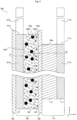
Figure 6 is a schematic cross-sectional view of a positive electrode and a negative electrode of a separatorless battery including a positive electrode and a negative electrode of another example according to the embodiment. -
Figure 7 is a schematic enlarged cross-sectional view of an interface and the vicinity thereof between a positive electrode second active material layer and a positive electrode electronic insulation layer of a positive electrode active material layer of a positive electrode of another example according to the embodiment. - Each embodiment of the present disclosure will be described with reference to the drawings. To facilitate understanding of each embodiment, the size and ratio of components may be exaggerated in each drawing. In the drawings, the same reference numerals are given to the same components. In the drawings, a lateral width direction X (X-axis direction), a depth direction Y (Y-axis direction), and a height direction Z (Z-axis direction) of the constituent members of the
battery 1 and thebattery 1 are indicated by arrows. In each of the drawings, the lateral width direction X, the depth direction Y, and the height direction Z indicate relative direction relationships. That is, for example, in a case where thebattery 1 is rotated by 180 degrees and the upper surface and the lower surface are reversely rotated, or in a case where thebattery 1 is rotated by 90 degrees and the upper surface is arranged as a side surface, the lateral width direction X, the depth direction Y, and the height direction Z of thebattery 1 change. - A configuration of the
battery 1 including thenegative electrode 120 according to the embodiment will be described with reference toFigures 1 to 4 . - As shown in
Figure 1 , thebattery 1 includes a charge/discharge body 100 in which electric power is charged and discharged, acontainer 200 which contains the charge/discharge body 100, and anexternal terminal 300 connected to the charge/discharge body 100 and attached to thecontainer 200. - As illustrated in
Figures 2 to 4 , the charge/discharge body 100 includes apositive electrode 110, anegative electrode 120, and aseparator 130. The charge/discharge body 100 impregnates theseparator 130 with an electrolyte in a state of being contained in thecontainer 200. As shown inFigures 2 and3 , the charge/discharge body 100 is configured by winding apositive electrode 110 formed in an elongated shape and anegative electrode 120 formed in an elongated shape through aseparator 130 formed in an elongated shape. The charge/discharge body 100 is formed in a rectangular parallelepiped shape in which both end portions are rounded in a state in which the constituent members are wound. - As illustrated in
Figures 3 and4 , thepositive electrode 110 includes a positive electrodecurrent collector layer 111 and a positive electrodeactive material layer 112 bonded to the positive electrodecurrent collector layer 111. - The positive electrode
current collector layer 111 is formed in an elongated shape extending in the lateral width direction X. As illustrated inFigures 3 and4 , the positive electrodecurrent collector 111 includes acurrent collector 111a and apositive electrode tab 111b. Thecurrent collector 111a is long in the lateral width direction X and is formed in a foil shape. As shown inFigure 4 , the positive electrodeactive material layer 112 is bonded to thecurrent collector 111a. The positive electrodeactive material layer 112 may be formed on both surfaces of thecurrent collector 111a. For example, the positive electrodeactive material layer 112 faces all regions along a shorter direction (height direction Z) of thecurrent collector 111a. As shown inFigures 3 and4 , thepositive electrode tab 111b protrudes from aside edge 111c along a longer direction of thecurrent collector 111a to the shorter direction (above the height direction Z) of thecurrent collector 111a. Thepositive electrode tab 111b is formed integrally with thecurrent collector 111a. For example, onepositive electrode tab 111b is formed on thecurrent collector 111a. Thecurrent collector 111a is formed of, for example, aluminum or an aluminum alloy, for example, an aluminum foil having a plate-like (sheet-like) shape. - The positive electrode
active material layer 112 includes a positive electrode active material composed of a lithium-containing composite oxide, a binder, and a conductive auxiliary agent. - Examples of the lithium-containing composite oxide include metallic elements such as nickel (Nickel), cobalt (Cobalt), and manganese (Manganese), and lithium (Lithium).
- Examples of the lithium-containing composite oxide may be a ternary lithium-containing composite oxide represented by the following formula:
Li1+XMAO2 (1)
(wherein X satisfies -0.15 ≤ X ≤ 0.15, and MA represents an element group containing at least one selected from the group consisting of Mn and Al, Ni, and Co.) The ternary lithium-containing composite oxide represented by the above general composition formula (1) has a high thermal stability and a stability in a high potential state, and the safety of thebattery 1 and various battery characteristics can be enhanced by applying the oxide. - As the binder, for example, polyvinylidene fluoride (PVdF), polytetrafluoroethylene (PTFE), polyethylene, polystyrene, polybutadiene, polyacrylonitrile, polyvinyl fluoride, polypropylene fluoride, polychloroprene fluoride, butyl rubber, nitrile rubber, styrene butadiene rubber (SBR), polysulfide rubber, nitrocellulose, cyanoethyl cellulose, various latexes, acrylic resins, or mixtures thereof can be used.
- As the conductive agent, a carbon-based material can be used. The carbon-based material may be crystalline carbon, amorphous carbon, or mixtures thereof. Examples of the crystalline carbon include artificial graphite, natural graphite (e.g., scaly graphite), or mixtures thereof. Examples of the amorphous carbon include carbon black (e.g., acetylene black, Ketjen black, channel black, furnace black, lamp black, thermal black, or mixtures thereof).
- The
positive electrode 110 can be formed, for example, as follows. The positive electrode active material and, optionally, the binder and the conductive agent are dispersed in a solvent (e.g., N-methyl-2-pyrrolidone (NMP), water) to prepare a paste-like or slurry-like positive electrode mixture composition. The positive electrode mixture composition is applied to the surface (one side or both sides) of the positive electrodecurrent collector layer 111, dried, and subjected to calendering if necessary to form a positive electrode mixture layer. As a result, thepositive electrode 110 is obtained. However, thepositive electrode 110 is not limited to the one manufactured by the above-described manufacturing method, and may be manufactured by another method. - As shown in
Figures 3 and4 , thenegative electrode 120 includes a negative electrodecurrent collector layer 121, a negative electrode first active material layer 122 (first active material layer) bonded to the negative electrodecurrent collector layer 121, and a negative electrode second active material layer 123 (second active material layer) bonded to the negative electrode firstactive material layer 122. That is, thenegative electrode 120 includes a plurality of active material layers. - The negative electrode
current collector layer 121 is formed in an elongated shape extending in the lateral width direction X. As illustrated inFigures 3 and4 , the negative electrodecurrent collector 121 includes acurrent collector 121a and anegative electrode tab 121b. Thecurrent collector 121a is long in the lateral width direction X and is formed in a foil shape. As shown inFigure 4 , thecurrent collector 121a has a longer width along the shorter direction (height direction Z) than thecurrent collector 111a of thepositive electrode 110. Both ends (from the upper end to the lower end in the height direction Z) of thenegative electrode 120 along the shorter direction of thecurrent collector 121a are positioned along the shorter direction of thecurrent collector 111a of thepositive electrode 110 via theseparators 130. The negative electrode firstactive material layer 122 are bonded to thecurrent collector 121a. The negative electrode firstactive material layer 122 may be formed on both surfaces of thecurrent collector 121a. As shown inFigures 3 and4 , thenegative electrode tab 121b protrudes from aside edge 121c along the longer direction of thecurrent collector 121a to the shorter direction (above the height direction Z) of thecurrent collector 121a. Thenegative electrode tab 121b protrudes in the same direction (upward in the height direction Z) as thepositive electrode tab 111b of thepositive electrode 110 while being laminated with thepositive electrode 110 via theseparators 130. Thenegative electrode tab 121b is spaced apart from thepositive electrode tab 111b of thepositive electrode 110 in the lateral width direction X while being laminated with thepositive electrode 110 via theseparators 130. Thenegative electrode tab 121b is formed integrally with thecurrent collector 121a. For example, onenegative electrode tab 121b is formed on thecurrent collector 121a. Thecurrent collector 121a is formed of, for example, copper or a copper alloy. The tensile strength of the negative electrodecurrent collector 121 is, for example, 30 kg/mm2 or higher. - As shown in
Figure 4 , the negative electrode firstactive material layer 122 is bonded to the negative electrodecurrent collector layer 121. The negative electrode firstactive material layer 122 corresponds to a high capacity layer in thenegative electrode 120. The high capacity layer means a layer capable of storing relatively large amounts of lithium ions. That is, the negative electrode firstactive material layer 122 corresponds to a lithium ion receiving layer capable of storing more lithium ions in thenegative electrode 120 than in the negative electrodecurrent collector layer 121. The negative electrode firstactive material layer 122 includes afirst graphite 122a and a first silicon simple substance orsilicon compound 122b of 1 wt% or more and 90 wt% or less with respect to the total weight of the negative electrode firstactive material layer 122. Weight percent is wt%, that is, weight percent concentration. - The
first graphite 122a is a negative electrode active material composed of a carbon-based material. The average particle diameter of thefirst graphite 122a is greater than the average particle diameter of thesecond graphite 123a. The average particle diameter of thefirst graphite 122a may be, for example, 10 µm or more and 35 µm or less in D50. In some embodiments, for example, the average particle diameter of thefirst graphite 122a may be 15 µm or more and 30 µm or less in D50. Here, D50 is a particle diameter when the integrated value is 50% in the particle size distribution measurement measured by a laser diffraction scattering type particle size distribution measurement method. In some embodiments, the content of thefirst graphite 122a may be, for example, 60 wt% or more and 98.5 wt% or less with respect to the total weight of the negative electrode firstactive material layer 122. In some embodiments, the content of thefirst graphite 122a may be, for example, 90 wt% or more and 98.5 wt% or less with respect to the total weight of the negative electrode firstactive material layer 122. In some embodiments, the content of thefirst graphite 122a may be, for example, 95 wt% or more and 98.5 wt% or less with respect to the total weight of the negative electrode firstactive material layer 122. - The first silicon simple substance or
silicon compound 122b is a negative electrode active material. Examples of the silicon compound include a silicon oxide, for example, SiO. The content of the first silicon simple substance orsilicon compound 122b is 1 wt% or more and 90 wt% or less with respect to the total weight of the negative electrode firstactive material layer 122. In an embodiment, the content of the first silicon simple substance orsilicon compound 122b may be, for example, 1 wt% or more and 50 wt% or less with respect to the total weight of the negative electrode firstactive material layer 122. In an embodiment, the content of the first silicon simple substance orsilicon compound 122b may be, for example, 1 wt% or more and 35 wt% or less with respect to the total weight of the negative electrode firstactive material layer 122. - The negative electrode first
active material layer 122 further includes, for example, at least onefirst binder 122c (binder) selected from the group consisting of rubber-based, acrylic-based, polyamideimide, and polyimide. The content of thefirst binder 122c may be, for example, 0.5 wt% or more and 10 wt% or less with respect to the total weight of the negative electrode firstactive material layer 122. In some embodiments, the content of thefirst binder 122c may be, for example, 1 wt% or more and 5 wt% or less with respect to the total weight of the negative electrode firstactive material layer 122. - The negative electrode first
active material layer 122 further includes, for example, a conductive auxiliary agent. Examples of the conductive auxiliary agent include carbon black such as acetylene black, Ketjen black, channel black, furnace black, lamp black, and thermal black. The amount of the conductive auxiliary agent or the like may be, for example, 0 wt% or more and 5 wt% or less with respect to the total weight of the negative electrode firstactive material layer 122. In an embodiment, the amount of the conductive auxiliary agent or the like may be, for example, 0 wt% or more and 3 wt% or less with respect to the total weight of the negative electrode firstactive material layer 122. - The thickness (first thickness T1) of one side of the negative electrode first
active material layer 122 in the laminating direction (depth direction Y) may be, for example, 5 µm or more and 500 µm or less in an average thickness. In an embodiment, the thickness (first thickness T1) of one side of the negative electrode firstactive material layer 122 in the laminating direction (depth direction Y) may be, for example, 10 µm or more and 300 µm or less in terms of the average thickness. In an embodiment, the thickness of the negative electrode firstactive material layer 122 in the laminating direction may be the same as the thickness of the negative electrode secondactive material layer 123 in the average thickness. - As shown in
Figure 4 , the negative electrode secondactive material layer 123 is bonded to the negative electrode firstactive material layer 122. The negative electrode secondactive material layer 123 corresponds to a high input/output layer in thenegative electrode 120. The high input/output layer means a layer capable of inputting and outputting lithium ions at a relatively high speed. That is, the negative electrode secondactive material layer 123 corresponds to a lithium ion receiving layer in which input and output of lithium ions are performed at a higher speed in thenegative electrode 120 than in the negative electrodecurrent collector layer 121. The negative electrode secondactive material layer 123 includes asecond graphite 123a having an average particle diameter in D50 smaller than thefirst graphite 122a, and a second silicon simple substance orsilicon compound 123b of 0 wt% or more and less than 1 wt% with respect to the total weight of the negative electrode secondactive material layer 123. In other words, in the embodiment, it is assumed that the negative electrode secondactive material layer 123 does not include asecond silicon 123b, for example. - The
second graphite 123a is a negative electrode active material composed of a carbon-based material. Thesecond graphite 123a may be the same as thefirst graphite 122a except for the average particle diameter described below. The average particle diameter in D50 of thesecond graphite 123a is smaller than the average particle diameter of thefirst graphite 122a. In some embodiments, for example, the average particle diameter of thesecond graphite 123a may be 2 µm or more and 15 µm or less in D50. In some embodiments, for example, the average particle diameter of thesecond graphite 123a may be 5 µm or more and 12 µm or less in D50. - The second silicon simple substance or
silicon compound 123b is a negative electrode active material. Examples of the silicon compound include a silicon oxide, for example, SiO. The second silicon simple substance orsilicon compound 123b may be the same material as the first silicon simple substance orsilicon compound 122b. The content of the second silicon simple substance orsilicon compound 123b may be, for example, 0 wt% or more and 1 wt% or less with respect to the total weight of the negative electrode secondactive material layer 123. In an embodiment, the content of the second silicon simple substance orsilicon compound 123b may be, for example, 0 wt% or more and 0.5 wt% or less with respect to the total weight of the negative electrode secondactive material layer 123. In some embodiments, the negative electrode secondactive material layer 123 may not include the second silicon simple substance orsilicon compound 123b. - The negative electrode second
active material layer 123 further includes, for example, at least onesecond binder 123c (binder) selected from the group consisting of rubber-based, acrylic-based, polyamideimide, and polyimide. Thesecond binder 123c may be the same as thefirst binder 122c. The content of thesecond binder 123c may be, for example, 0.2 wt% or more and 5 wt% or less with respect to the total weight of the negative electrode secondactive material layer 123. In some embodiments, the content of thesecond binder 123c may be, for example, 0.5 wt% or more and 2 wt% or less with respect to the total weight of the negative electrode secondactive material layer 123. - The negative electrode second
active material layer 123 further includes, for example, at least one additional carbon selected from the group consisting of an easily graphitizable carbon, a hardly graphitizable carbon, an amorphous carbon, and a low crystalline carbon. The easily graphitizable carbon corresponds to soft carbon. The non-graphitic carbon corresponds to a hard carbon. The amorphous carbon corresponds to amorphous carbon. The amorphous carbon is, for example, carbon black such as acetylene black, Ketjen black, channel black, furnace black, lamp black, and thermal black. The amount of the additional carbon may be, for example, 0 wt% or more and 50 wt% or less with respect to the total weight of the negative electrode secondactive material layer 123. In some embodiments, the amount of additional carbon may be 5 wt% or more and 50 wt% or less with respect to the total weight of the negative electrode secondactive material layer 123, for example. In some embodiments, the amount of additional carbon may be 10 wt% or more and 40 wt% or less with respect to the total weight of the negative electrode secondactive material layer 123, for example. - The additional carbon serves as, for example, a conductive auxiliary agent or the like. The amount of the conductive auxiliary agent or the like may be, for example, 0 wt% or more and 5 wt% or less with respect to the total weight of the negative electrode second
active material layer 123. In an embodiment, the amount of the conductive auxiliary agent or the like may be, for example, 0 wt% or more and 3 wt% or less with respect to the total weight of the negative electrode secondactive material layer 123. - The thickness (second thickness T2) of one side of the negative electrode second
active material layer 123 in the laminating direction (depth direction Y) may be, for example, 5 µm or more and 500 µm or less in terms of the average thickness. In an embodiment, the thickness (second thickness T2) of one side of the negative electrode secondactive material layer 123 in the laminating direction (depth direction Y) may be, for example, 10 µm or more and 300 µm or less in terms of the average thickness. In an embodiment, the thickness of the negative electrode secondactive material layer 123 in the laminating direction may be the same as the thickness of the negative electrode firstactive material layer 122 in the average thickness. - As shown in
Figures 3 and4 , theseparator 130 has an insulating function of insulating between thepositive electrode 110 and thenegative electrode 120 and preventing a short circuit between thepositive electrode 110 and thenegative electrode 120, and a function of holding a nonaqueous electrolyte. Theseparator 130 allows lithium ions to pass through the electrolyte. Theseparator 130 is formed in an elongated shape. As shown inFigure 4 , theseparators 130 are longer in width along the shorter direction (height direction Z) than thecurrent collector 111a of thepositive electrode 110 and thecurrent collector 121a of thenegative electrode 120. Both ends (from upper end to lower end in the height direction Z) of thepositive electrode 110 along the shorter direction of thecurrent collector 111a are located within a range (from upper end to lower end in the height direction Z) along the shorter direction of theseparators 130, and both ends (from upper end to lower end in the height direction Z) along the shorter direction of thecurrent collector 121a of thenegative electrode 120 are located. Theseparator 130 is made of a porous material. As theseparator 130, a porous sheet made of a resin such as polyethylene (PE: PolyEthylene), polypropylene (PP: PolyPropylene), polyester, cellulose, or polyamide, or a laminated sheet thereof (for example, a sheet having a three-layer structure of PP/PE/PP) is used. - One or both surfaces of the
separator 130 may be provided with a layer including an inorganic material (e.g., alumina particles etc.) and a binder. Thus, even when thebattery 1 is used in an abnormal state (for example, when the temperature of the lithium ion secondary battery rises to 160 °C or higher due to overcharge, crushing, etc.), theseparator 130 is prevented from melting and the insulating function can be maintained. Therefore, the safety of thebattery 1 is improved. - The electrolyte corresponds to a so-called electrolyte. The electrolyte is impregnated into the
separator 130 and is in contact with thepositive electrode 110 and thenegative electrode 120. The electrolyte includes an organic solvent, a support salt, and an additive. As the organic solvent, for example, a carbonate ester or the like is used. As the support salt, for example, a lithium salt is used. As the additive, for example, vinylene carbonate or fluoroethylene carbonate is used. - As shown in
Figure 1 , thecontainer 200 contains a charge/discharge body 100. Thecontainer 200 includes acase 201 and alid 202. Thelid 202 is joined to the opening of thecase 201, and seals the charge/discharge body 100 together with thecase 201. The charge/discharge body 100 sealed by thecase 201 and thelid 202 is filled with an electrolyte. - As illustrated in
Figure 1 , theexternal terminal 300 includes apositive electrode terminal 301 and anegative electrode terminal 302. Thepositive electrode terminal 301 and thenegative electrode terminal 302 relay input and output of electric power between the charge/discharge body 100 and an external device. In addition, in a case where a battery pack is configured by using a plurality ofbatteries 1, the othernegative electrode terminal 302 adjacent to one of the adjacentpositive electrode terminals 301 is joined via a bus bar. Thepositive electrode terminal 301 is indirectly or directly bonded to thepositive electrode tab 111b via a positive electrode current collector plate. Thenegative electrode terminal 302 is indirectly or directly bonded to thenegative electrode tab 121b via a negative electrode current collector plate. Thepositive electrode terminal 301 and thenegative electrode terminal 302 are attached to thelid 202. - The
battery 1 including thenegative electrode 120 and thenegative electrode 120 can be manufactured by using a known technique in this technical field, except for manufacturing thenegative electrode 120 by coating a negative electrode mixture composition of the negative electrode firstactive material layer 122 described above (that is, the composition containing a material contained in the negative electrode firstactive material layer 122 and a solvent such as N-methyl-2-pyrrolidone (NMP) and/or water) on the negative electrodecurrent collector layer 121 by a known technique, and by coating a negative electrode mixture composition of the negative electrode secondactive material layer 123 described above (that is, the composition containing a material contained in the negative electrode secondactive material layer 123 and a solvent such as N-methyl-2-pyrrolidone (NMP) and/or water) on the negative electrode firstactive material layer 122 by a known technique. - For example, the
negative electrode 120 can be formed as follows. First, materials included in the negative electrode firstactive material layer 122 are prepared. The materials may be particulate. The materials are dispersed in a solvent (e.g., N-methyl-2-pyrrolidone (NMP) and/or water) to prepare a negative electrode mixture composition for the negative electrode firstactive material layer 122 in a pasty or slurry form. The prepared negative electrode mixture composition is applied to a surface (one side or both sides) of the negative electrodecurrent collector layer 121, dried, and subjected to calendering if necessary to form the negative electrode firstactive material layer 122. Further, materials included in the negative electrode secondactive material layer 123 are prepared. The materials may be particulate. The materials are dispersed in a solvent (e.g., N-methyl-2-pyrrolidone (NMP) and/or water) to prepare a negative electrode mixture composition for the negative electrode secondactive material layer 123 in a pasty or slurry form. The prepared negative electrode mixture composition is applied to the surface (one side or both sides) of the negative electrode firstactive material layer 122, dried, and subjected to calendering if necessary to form the negative electrode secondactive material layer 123. As a result, thenegative electrode 120 is obtained. However, thenegative electrode 120 is not limited to the one manufactured by the above-described manufacturing method, and may be manufactured by another method. - Further, as the method for manufacturing the
negative electrode 120 according to the embodiment, a manufacturing method in which the negative electrode first active material layer and the negative electrode second active material layer of the negative electrode active material layer are simultaneously coated may be used. Hereinafter, this manufacturing method will be described with reference toFigure 5 . - In this manufacturing method, materials (for example, a negative electrode active material, a conductive auxiliary agent, a binder, or the like) included in the negative electrode first active material layer are prepared. These materials are mixed and the resulting mixture is dispersed in a solvent (e.g., N-methyl-2-pyrrolidone (NMP) and/or water) to obtain a negative electrode first slurry. Further, materials (for example, a negative electrode active material, a conductive auxiliary agent, a binder, or the like) included in the negative electrode second active material layer are prepared. These materials are mixed and the resulting mixture is dispersed in a solvent (e.g., N-methyl-2-pyrrolidone (NMP) and/or water) to obtain a negative electrode second slurry.
- Next, for example, the negative electrode first slurry and the negative electrode second slurry are simultaneously applied onto the negative electrode
current collector 34a using thedie head 50 as shown inFigure 5 . Thedie head 50 has anoutlet block 57, a three-dimensional shim 58, and aninlet block 59. Inside thedie head 50, a negative electrodesecond slurry manifold 52 and a negative electrodefirst slurry manifold 51 are provided. The negative electrode second slurry and the negative electrode first slurry are simultaneously discharged from themanifolds current collector 34a conveyed along theback roller 56. Thereby, the negative electrodesecond slurry layer 33d and the negative electrodefirst slurry layer 33b are formed. Next, the negative electrodefirst slurry layer 33b and the negative electrodesecond slurry layer 33d are dried by volatilizing the solvents contained in the negative electrodefirst slurry layer 33b and the negative electrodesecond slurry layer 33d in a drying oven etc. Thereby, a negative electrode first active material layer (not shown) and a negative electrode second active material layer (not shown) are formed on one surface of the negative electrodecurrent collector 34a. Next, the negative electrodecurrent collector 34a, the negative electrode first active material layer, and the negative electrode second active material layer are pressed. Specifically, the laminate including the negative electrodecurrent collector 34a, the negative electrode first active material layer, and the negative electrode second active material layer is sandwiched between rollers heated to 60 to 120 °C and is pressed. Thereafter, the laminate is slit to a predetermined width. Thereby, a negative electrode is obtained. - In the battery including the negative electrode manufactured by the manufacturing process to which the simultaneous coating of the two or more layers is applied, since the interface between the negative electrode
first slurry layer 33b and the negative electrodesecond slurry layer 33d has the uneven shape, the adhesion of the negative electrodefirst slurry layer 33b and the negative electrodesecond slurry layer 33d is improved, and the reliability of the battery can be improved without the two layers being peeled off even if the volume change due to charge and discharge occurs. - The effect of the
battery 1 including thenegative electrode 120 of the embodiment will be described with reference toFigure 4 . - The first active material layer (negative electrode first active material layer 122) of the
negative electrode 120 includes afirst graphite 122a and a first silicon simple substance orsilicon compound 122b of 1 wt% or more and 90 wt% or less with respect to the total weight of the negative electrode firstactive material layer 122. The second active material layer (negative electrode second active material layer 123) of thenegative electrode 120 includes asecond graphite 123a having an average particle diameter smaller than that of the first graphite, and a second silicon simple substance orsilicon compound 123b of 0 wt% or more and less than 1 wt% with respect to the total weight of the negative electrode secondactive material layer 123. Thebattery 1 includes thenegative electrode 120, apositive electrode 110, and an electrolyte. - According to such a configuration, the durability of the
battery 1 is improved. Therefore, by improving the durability of thebattery 1, deterioration of thenegative electrode 120 due to repeated charging and discharging of thebattery 1 can be suppressed, and thereby deterioration of the charging and discharging cycle characteristics of thebattery 1 can be suppressed. Therefore, thebattery 1 can be rapidly charged while suppressing a decrease in life. - Specifically, in the
negative electrode 120, the negative electrode firstactive material layer 122 includes afirst graphite 122a having a relatively large average particle diameter (i.e., a small specific surface area) as compared with the average particle diameter of thesecond graphite 123a included in the negative electrode secondactive material layer 123. Thefirst graphite 122a and thesecond graphite 123a in thenegative electrode 120 may react with the electrolyte and form a film on the graphite surfaces as thebatteries 1 are charged and discharged. The film traps lithium ions and reduces the lithium ion storability of the graphite. Therefore, in order to improve the lithium ion storability of the negative electrode firstactive material layer 122, it is sufficient to prevent the film from being formed, and in order to prevent the film from being formed, it is sufficient to reduce the surface area of the graphite which reacts with the electrolyte, that is, to reduce the specific surface area of the graphite (that is, increase the average particle diameter). Therefore, in thenegative electrode 120, by making the average particle diameter of thefirst graphite 122a contained in the negative electrode firstactive material layer 122 larger than the average particle diameter of thesecond graphite 123a contained in the negative electrode secondactive material layer 123, the amount of film that can be formed by reacting the graphite with the electrolyte is reduced, and good storage properties of lithium ions are ensured, and consequently, the negative electrode firstactive material layer 122 can function as a high capacity layer of thenegative electrode 120. - Further, the negative electrode first
active material layer 122 contains the first silicon simple substance orsilicon compound 122b in an amount of 1 wt% or more and 90 wt% or less with respect to the total weight of the negative electrode firstactive material layer 122. When the negative electrode firstactive material layer 122 contains the first silicon simple substance orsilicon compound 122b having excellent lithium ion storability, the capacity of thebattery 1 can be increased. - The negative electrode first
active material layer 122 may include, for example, at least onefirst binder 122c selected from the group consisting of rubber-based, acrylic-based, polyamideimide, and polyimide. - According to such a configuration, even if the first silicon simple substance or
silicon compound 122b contained in the negative electrode firstactive material layer 122 expands or contracts relatively significantly during the charging and discharging of thebattery 1, the decrease in the tensile strength of the negative electrodecurrent collector layer 121 and/or the negative electrode firstactive material layer 122 and/or the negative electrode secondactive material layer 123 due to the repeated input of stresses of thefirst binder 122c can be made relatively small. That is, the decrease over time in the tensile strength of the negative electrodecurrent collector layer 121 and/or the negative electrode firstactive material layer 122 and/or the negative electrode secondactive material layer 123 due to the expansion or contraction of the first silicon simple substance orsilicon compound 122b caused by the repetition of the charging and discharging of thebattery 1 is relatively small as compared with the case where the binder is not included due to thefirst binder 122c. More specifically, even if the first silicon simple substance orsilicon compound 122b contained in the negative electrode firstactive material layer 122 expands relatively significantly when thebattery 1 is charged, thefirst binder 122c can sufficiently retain the first silicon simple substance orsilicon compound 122b. The fact that thefirst binder 122c can sufficiently retain the first silicon simple substance orsilicon compound 122b means that the first silicon simple substance orsilicon compound 122b can be sufficiently maintained to be fixed to the negative electrodecurrent collector layer 121 and/or the negative electrode secondactive material layer 123 by thefirst binder 122c, for example. On the other hand, even if the first silicon simple substance orsilicon compound 122b contained in the negative electrode firstactive material layer 122 shrinks relatively large during discharging of thebattery 1, the first silicon simple substance orsilicon compound 122b can be sufficiently maintained by thefirst binder 122c. That is, even if the first silicon simple substance orsilicon compound 122b contained in the negative electrode firstactive material layer 122 relatively significantly expands or contracts with the charging and discharging of thebattery 1, the separation between the negative electrode firstactive material layer 122 and the negative electrodecurrent collector layer 121 and/or the negative electrode secondactive material layer 123 can be suppressed. That is, deterioration of the battery characteristics of the charge/discharge body 100 can be suppressed. As a result, deterioration in the quality of thenegative electrode 120 due to repeated charging and discharging of thebattery 1 can be suppressed, deterioration in a charge-discharge cycle characteristics of thebattery 1 can be suppressed, and the life of thebattery 1 can be extended. - For example, the negative electrode
current collector 121 may have a tensile strength of 30 kg/mm2 or higher. - According to such a configuration, even if the first silicon simple substance or
silicon compound 122b contained in the negative electrode firstactive material layer 122 relatively significantly expands or contracts with the charging and discharging of thebattery 1, the expansion or contraction can be suppressed by the negative electrodecurrent collector layer 121 bonded to the negative electrode firstactive material layer 122. Therefore, separation between the negative electrodecurrent collector layer 121 and the negative electrode firstactive material layer 122 can be suppressed. In addition, since the first silicon simple substance orsilicon compound 122b contained in the negative electrode firstactive material layer 122 is suppressed from being relatively greatly expanded or contracted, separation of the negative electrode secondactive material layer 123 bonded to the negative electrode firstactive material layer 122 and the negative electrode firstactive material layer 122 can be suppressed. That is, deterioration of the battery characteristics of the charge/discharge body 100 can be suppressed. As a result, deterioration in the quality of thenegative electrode 120 due to the repeated charging and discharging of thebattery 1 can be suppressed, deterioration in the charge-discharge cycle characteristics of thebattery 1 can be suppressed, and the life of thebattery 1 can be extended. - In the
negative electrode 120, the negative electrode secondactive material layer 123 includes asecond graphite 123a having an average particle diameter (that is, a smaller volume) that is relatively smaller than the average particle diameter of thefirst graphite 122a included in the negative electrode firstactive material layer 122. The smaller the volume of the graphite, the shorter the migration distance of the lithium ions therein, so that the lithium ions can be input and output at high speed. Therefore, in thenegative electrode 120, by making the average particle diameter of thesecond graphite 123a contained in the negative electrode secondactive material layer 123 smaller than the average particle diameter of thefirst graphite 122a contained in the negative electrode firstactive material layer 122, lithium ions can be input and output at high speed, and consequently, the negative electrode secondactive material layer 123 can function as the high input and output layer of thenegative electrode 120. - Further, the negative electrode second
active material layer 123 contains the second silicon simple substance orsilicon compound 123b in an amount of 0 wt% or more and less than 1 wt% with respect to the total weight of the negative electrode secondactive material layer 123. In other words, the ratio of the second silicon simple substance orsilicon compound 123b in the negative electrode secondactive material layer 123 is smaller than the ratio of the first silicon simple substance orsilicon compound 122b in the negative electrode firstactive material layer 122. The first silicon simple substance orsilicon compound 122b and the second silicon simple substance orsilicon compound 123b in thenegative electrode 120 expand as thebattery 1 is charged, and contract as thebattery 1 is discharged. Accordingly, since the negative electrode secondactive material layer 123 includes a second silicon simple substance orsilicon compound 123b less than the first silicon simple substance orsilicon compound 122b contained in the negative electrode firstactive material layer 122, expansion or contraction of the second silicon simple substance orsilicon compound 123b in the negative electrode secondactive material layer 123 that may occur with the charging and discharging of thebattery 1 is suppressed, and separation of the negative electrode secondactive material layer 123 from the negative electrode firstactive material layer 122 is suppressed, and consequently, durability of thebattery 1 and rapid charge characteristics of thebattery 1 contradictory to the high energy density of thebattery 1 can be improved. - The negative electrode second
active material layer 123 may include, for example, at least one selected from the group consisting of an easily graphitizable carbon, a hardly graphitizable carbon, an amorphous carbon, and a low crystalline carbon. - According to such a configuration, lithium ions can be input and output at a relatively high speed depending on at least one selected from the group consisting of the easily graphitizable carbon, the hardly graphitizable carbon, the amorphous carbon, and the low crystalline carbon. That is, the negative electrode second
active material layer 123 can function as a high input/output layer of thenegative electrode 120. As a result, it is possible to quickly charge thebattery 1 while suppressing a decrease in the life of thebattery 1. - Experimental results of the
battery 1 including thenegative electrode 120 of the embodiment will be described with reference to Tables 1 to 3. Tables 1 and 2 show the configurations of the batteries of Examples 1 to 13 and Comparative Examples 1 to 5, and Table 3 shows the test results (the capacity after one cycle and 100 cycles, and a direct current resistance (DCR) after one cycle) of the batteries. The battery capacity, charge/discharge cycle, and the DCR are measured as follows. - Regarding the battery capacity, constant voltage-constant current charging (CC-CV charging) until the battery voltage becomes 4.2 V was performed at the charging current 1C for a total of 2.5 hours. After 30 minutes of pause, constant current discharge (CC discharge) was performed at a discharge current 0.2C up to the battery voltage 2.9 V to obtain an initial capacity.
- In the charge/discharge cycle test, 99 times of charge/discharge were repeated after the battery capacity was measured. Constant voltage-constant current charging (CC-CV charging) was performed at a charging current 1C for a total of 2.5 hours until the battery voltage became 4.2 V. After 30 minutes of pause, the constant current discharge (CC discharge) was performed at a discharge current 1C up to the battery voltage 2.9 V. It was then paused for 30 minutes. The battery capacity was measured again after the charge-discharge cycle, and compared with the initial battery capacity.
- The relationship between SOC and open circuit voltage (OCV) was obtained by using the voltage after discharging the battery capacity from 4.2 V in increments of 5 % of the battery capacity and pausing for 2 hours as an OCV, and the relationship with the SOC was obtained.
- Regarding a DCR of SOC 25 % that is a low SOC range, a CC-CV charging was carried out from SOC 0 % to SOC 25 % at charge current of 1C using the relationship of SOC-OCV. Next, the lithium ion secondary battery was held in a thermostatic bath at -10 °C for 5 hours. After that, the lithium ion secondary battery was discharged at a constant current of 0.5C for 10 seconds, and a voltage drop value caused by the discharge was measured. Further, similar constant current discharges were performed with discharge currents 1C, 1.5C and 2C. The discharge current is plotted on the horizontal axis and the voltage drop value is plotted on the vertical axis, and a slope of the graph is determined as a DCR. The DCR (relative value) of the lithium ion secondary batteries of Examples and Comparative Examples were calculated, the DCR of the lithium ion secondary battery of Example 1 being normalized to 100. The lower the DCR in SOC 25 %, the lower an internal resistance of the lithium ion secondary battery in the low SOC range.
-
Table 1 First Active Material Layer Second Active Material Layer Concentration of SiO (wt%) Average Particle Diameter of Graphite D50 (µm) Binder Concentration of SiO (wt%) Average Particle Diameter of Graphite D50 (µm) Amorphous Carbon Example 1 10 20 SBR 0 8 Added Example 2 30 20 SBR 0 8 Added Example 3 10 12 SBR 0 8 Added Example 4 10 30 SBR 0 8 Added Example 5 10 20 SBR 0.5 8 Added Example 6 10 20 SBR 0 3 Added Example 7 10 20 SBR 0 12 Added Example 8 10 20 SBR 0 8 Not Added Example 9 10 20 AR 0 8 Added Example 10 10 20 PI 0 8 Added Example 11 10 20 SBR 0 8 Added Example 12 10 20 SBR 0 8 Added Example 13 10 20 SBR 0 8 Added Comparative Example 1 - - - 0 8 Added Comparative Example 2 10 20 SBR - - - Comparative Example 3 0 20 SBR 0 8 Added Comparative Example 4 95 20 SBR 0 8 Added Comparative Example 5 10 20 SBR 10 8 Added SBR: Styrene Butadiene Rubber
AR: Acrylic Resin
PI: Polyimide
wt%: Concentration Relative to The Total Weight of Each Active Material Layer D50: -
Table 2 Current Collector Layer Active Material Layer Tensile Strength (kg/mm2) Thickness of First Active Material Layer/ Thickness of Second Active Material Layer Example 1 50 1/1 Example 2 50 1/1 Example 3 50 1/1 Example 4 50 1/1 Example 5 50 1/1 Example 6 50 1/1 Example 7 50 1/1 Example 8 50 1/1 Example 9 50 1/1 Example 10 50 1/1 Example 11 30 1/1 Example 12 50 1/2 Example 13 50 2/1 Comparative Example 1 50 0/1 Comparative Example 2 50 1/0 Comparative Example 3 50 1/1 Comparative Example 4 50 1/1 Comparative Example 5 50 1/1 Thickness Ratio: Thickness of First Active Material Layer (First Thickness T1)/
Thickness of Second Active Material Layer (Second Thickness T2) -
Table 3 Capacity (%) DCR (%) After One Cycle * After Initial Charge After 100 cycles Example 1 100 * Standard Value 85 100 * Standard Value Example 2 153 80 100 Example 3 100 84 98 Example 4 100 86 102 Example 5 101 83 100 Example 6 100 84 95 Example 7 100 86 105 Example 8 100 86 120 Example 9 100 86 98 Example 10 99 89 102 Example 11 100 83 100 Example 12 98 87 95 Example 13 102 83 105 Comparative Example 1 93 95 90 Comparative Example 2 107 74 130 Comparative Example 3 93 95 100 Comparative Example 4 253 60 95 Comparative Example 5 107 73 100 Capacity [Ah]: Relative Value When Value After One Cycle of Example 1 Is Defined as 100 % (* Standard Value)
DCR [Ω]: Relative Value When DCR of Example 1 Is Defined as 100% (* Standard Value)
Test Temperature = -10 °C, Discharge Time = 10 s, SOC = 25 % - Tables 1 to 3 showed the following: Here, Example 1 and Examples 2 to 13 or Comparative Examples 1 to 5 are compared with respect to Example 1. In addition, the capacity is preferably larger, the DCR is a property related to rapid charge and is preferably smaller.
- Examples 1 and 2 to 13 are compared. In Example 2, it was found that when the first silicon simple substance or
silicon compound 122b in the negative electrode firstactive material layer 122 was increased to 30 wt% with respect to the total weight of the negative electrode firstactive material layer 122, the capacity after 100 cycles was slightly decreased, but the capacity after one cycle was increased to about 1.5 times. In Example 3, it was found that when the average particle diameter D50 of thefirst graphite 122a in the negative electrode firstactive material layer 122 was larger than 8 µm, which is the average particle diameter D50 of thesecond graphite 123a in the negative electrode secondactive material layer 123, but the average particle diameter was decreased to 12 µm, the capacity after 100 cycles was slightly decreased, but the direct current resistance (DCR) was decreased. In Example 4, it was found that when the average particle diameter D50 of thefirst graphite 122a in the negative electrode firstactive material layer 122 was increased to 30 µm, the capacity after 100 cycles increased although the DCR was slightly increased. In Example 5, it was found that when 0.5 wt% of the second silicon simple substance orsilicon compound 123b was added to the negative electrode secondactive material layer 123 with respect to the total weight of the negative electrode secondactive material layer 123, the capacity after 100 cycles was slightly decreased, but the capacity after one cycle was increased. In Example 6, it was found that when the average particle diameter D50 of thesecond graphite 123a in the negative electrode secondactive material layer 123 was reduced to 3 µm, the capacity after 100 cycles was slightly reduced, but the DCR was reduced. In Example 7, it was found that when the average particle diameter D50 of thesecond graphite 123a in the negative electrode secondactive material layer 123 was smaller than 20 µm, which is the average particle diameter D50 of thefirst graphite 122a in the negative electrode firstactive material layer 122, but increased to 12 µm, the DCR became slightly larger, but the capacity after 100 cycles increased. In Example 8, it was found that when amorphous carbon was not added to the negative electrode secondactive material layer 123, the DCR increased, but the capacity after 100 cycles increased. In Example 9, it was found that when thefirst binder 122c in the negative electrode firstactive material layer 122 was changed to an acrylic resin (AR), the capacity after 100 cycles increased and the DCR decreased. In Example 10, it was found that when thefirst binder 122c in the negative electrode firstactive material layer 122 was changed to polyimide (PI), the capacity after one cycle decreased and the DCR increased, but the capacity after 100 cycles increased. In Example 11, it was found that when the tensile strength of the negative electrodecurrent collector layer 121 was reduced to 30 kg/mm2, the capacity after 100 cycles was slightly reduced, but the performance almost equivalent to that of Example 1 could be maintained. In Example 12, it was found that when the thickness of the negative electrode firstactive material layer 122 in the laminating direction was reduced to 1/2 of the thickness of the negative electrode secondactive material layer 123 in the laminating direction, the capacity after one cycle slightly decreased, but the capacity after 100 cycles increased and the DCR decreased. In Example 13, it was found that when the thickness of the negative electrode firstactive material layer 122 in the laminating direction was increased up to twice the thickness of the negative electrode secondactive material layer 123 in the laminating direction, the capacity after 100 cycles slightly decreased and the DCR slightly increased, but the capacity after one cycle increased. - Next, Example 1 and Comparative Examples 1 to 5 are compared. In Comparative Example 1, it was found that when the negative electrode first
active material layer 122 was not present, the capacity after 100 cycles was increased and the DCR was decreased, but the capacity after one cycle was greatly decreased. In Comparative Example 2, it was found that when the negative electrode secondactive material layer 123 was not present, the capacity after one cycle was slightly increased, but the capacity after 100 cycles was significantly decreased and the DCR was also significantly increased. In Comparative Example 3, it was found that when the first silicon simple substance orsilicon compound 122b was not added to the negative electrode firstactive material layer 122, the capacity after 100 cycles was increased, but the capacity after one cycle was greatly decreased. In Comparative Example 4, it was found that when the first silicon simple substance orsilicon compound 122b was added to the negative electrode firstactive material layer 122 in the amount of 95 wt% with respect to the total weight of the negative electrode firstactive material layer 122, the capacity after one cycle was increased by about 2.5 times, and although the DCR was slightly reduced, the capacity after 100 cycles was greatly reduced. In Comparative Example 5, it was found that when the second silicon simple substance orsilicon compound 123b was added to the negative electrode secondactive material layer 123 in an amount of up to 10 wt% with respect to the total weight of the negative electrode secondactive material layer 123, the capacity after one cycle was slightly increased, but the capacity after 100 cycles was significantly decreased. - Therefore, by comparison between Example 1 and one or more of Examples 2 to 13 and Comparative Examples 1 to 5, the negative electrode and the battery of the above-described embodiment have the following configuration, or preferably have the following configuration.
- Comparing Example 1 with Comparative Examples 1 and 2, the
negative electrode 120 includes a negative electrode firstactive material layer 122 and a negative electrode secondactive material layer 123. Comparing Example 1 with Example 2 and Comparative Examples 3 and 4, the negative electrode firstactive material layer 122 includes a first silicon simple substance orsilicon compound 122b of 1 wt% or more and 90 wt% or less with respect to the total weight of the negative electrode firstactive material layer 122. Comparing Example 1 with Examples 3, 4, 6 and 7, it is preferable that the negative electrode firstactive material layer 122 contains afirst graphite 122a having an average particle diameter larger than that of the negative electrode secondactive material layer 123, specifically, the negative electrode firstactive material layer 122 contains afirst graphite 122a having an average particle diameter larger than that of thesecond graphite 123a contained in the negative electrode secondactive material layer 123 and in D50 of 10 µm or more and 35 µm or less, and the negative electrode secondactive material layer 123 contains asecond graphite 123a having an average particle diameter smaller than that of thefirst graphite 122a contained in the negative electrode firstactive material layer 122 and in D50 of 2 µm or more and 15 µm or less. Comparing Example 1 with Example 5 and Comparative Example 5, the negative electrode secondactive material layer 123 contains 0 wt% or more and less than 1 wt% of the second silicon simple substance orsilicon compound 123b with respect to the total weight of the negative electrode secondactive material layer 123. Comparing Example 1 with Example 8, it is preferable that the negative electrode secondactive material layer 123 further contains at least one additional carbon selected from the group consisting of an easily graphitizable carbon, a hardly graphitizable carbon, an amorphous carbon, and a low crystalline carbon, particularly the amorphous carbon. Comparing Example 1 with Examples 9 and 10, it is preferable that the negative electrode firstactive material layer 122 further includes afirst binder 122c, and specifically, the negative electrode firstactive material layer 122 further includes at least onefirst binder 122c selected from the group consisting of rubber-based, acrylic-based, polyamideimide, and polyimide. Comparing Example 1 with Example 11, the tensile strength of the negative electrodecurrent collector 121 is preferably 30 kg/mm2 or higher, particularly 40 kg/mm2 or higher. Comparing Example 1 with Examples 12 and 13, the thickness of the negative electrode firstactive material layer 122 in the laminating direction can be changed depending on the characteristics of the battery to be obtained. - The negative electrode and the lithium ion secondary battery of the present disclosure are not limited to the configuration of the lithium ion
secondary battery 1 described in the embodiment, and can be appropriately configured based on the contents described in the claims. - The embodiments have been described in detail or simply in order to clearly explain the present disclosure, and it is not necessary for the embodiments to include all of the configurations described, or the embodiments may include configurations that are not illustrated. In addition, a part of the configuration of the embodiment may be deleted, replaced with the configuration of the other embodiments, or a combination of the configurations of the other embodiments.
- The lithium ion
secondary battery 1 is not limited to a battery that is mounted on an electric vehicle and supplies electric power to a driving motor of the electric vehicle. For example, the lithium ionsecondary battery 1 can be applied to a battery mounted on a portable electronic device such as a smartphone (registered trademark) or a battery mounted on a stationary power generation device. - The
negative electrode 120 is not limited to a configuration in which two or more types of active material layers are provided in the negative electrodecurrent collector layer 121. For example, thenegative electrode 120 may be configured such that three or more types of active material layers are provided in the negative electrodecurrent collector layer 121. - The
negative electrode 120 is not limited to a configuration in which two types of active material layers are provided only on one side of the negative electrodecurrent collector layer 121. For example, thenegative electrode 120 may be configured such that two types of active material layers are provided on both sides of the negative electrodecurrent collector layer 121. In thenegative electrode 120, two types of active material layers may be provided on one side of the negative electrodecurrent collector layer 121, and one type of active material layer may be provided on the other side of the negative electrodecurrent collector layer 121. - The
negative electrode 120 is not limited to a configuration in which anegative electrode tab 121b protruding from the negative electrodecurrent collector 121a is provided. For example, thenegative electrode 120 may be configured such that an end portion of the wound negative electrodecurrent collector 121a is electrically connected to thenegative electrode terminal 302 via the negative electrode current collector plate. In addition, thenegative electrode 120 may be configured such that an end portion of the wound negative electrodecurrent collector 121a is electrically connected to thenegative electrode terminal 302. - The charge/
discharge body 100 is not limited to a wound type in which an elongatedpositive electrode 110 and an elongatednegative electrode 120 are wound through anelongated separator 130. For example, the charge/discharge body 100 may be configured by a laminated type in which a plurality of positive electrodes, a plurality of separators, and a plurality of negative electrodes each having a rectangular shape are laminated. Further, the charge/discharge body 100 may be configured as a laminated type in which a plurality of positive electrodes and a plurality of negative electrodes formed in a relatively short shape are alternately provided with respect to one separator formed in a long shape while being opposed to each other via a separator. In the charge/discharge body 100 having such a configuration, the positive electrode and the negative electrode face each other via the separator by folding and laminating the separators. - The
separator 130 that insulates thepositive electrode 110 and thenegative electrode 120 may be formed of an insulating member laminated on the electrode. The insulating member is bonded to thepositive electrode 110 or thenegative electrode 120. The insulating member preferably has heat resistance. For example, ceramics is used as the insulating member. Such a configuration corresponds to a so-called separatorless configuration. In addition to theseparator 130, an insulating member may be used, that is, both theseparator 130 and the insulating member may be used. - The lithium ion
secondary battery 1 is not limited to a configuration in which the charge/discharge body 100 is sealed by thecase 201 and thelid 202. For example, the lithium ionsecondary battery 1 may be configured by sealing the charge/discharge body 100 with a laminate film. - The lithium ion
secondary battery 1 is not limited to a configuration in which a liquid electrolyte is used. For example, the lithium ionsecondary battery 1 may be configured as an all-solid-state secondary battery. - Further, the battery according to the embodiment may be a battery including a solid electrolyte as an electrolyte, and may include a positive electrode, a negative electrode, and a solid electrolyte layer including the solid electrolyte, and a charge/discharge body in which the solid electrolyte layer is interposed between the positive electrode and the negative electrode. For example, each of the positive electrode electronic insulation layer and the negative electrode electronic insulation layer includes a solid electrolyte. Both of the positive electrode electronic insulation particles and the negative electrode electronic insulation particles are solid electrolyte particles.
- The battery including such a solid electrolyte does not need to include an electrolyte solution, and thus can have high safety.
- Examples of solid electrolytes include sulphide-based solid electrolytes, such as Li10GeP2S12, Li6PS5Cl and Li2S-P2S5 glasses, Li2S-SiS2 glasses, Li2S-P2S5-GeS2 glasses, Li2S-B2S3 glasses, oxide-based solid electrolytes, such as Li7La3Zr2O12, LiLaTiO3, LiTi(PO4)3, LiGe(PO4)3 and complex hydride solid electrolytes, such as LiBH4-LiI, LiBH4-LiNH2, and mixtures of two or more of these.
- The battery including the negative electrode of another example according to the embodiment may be a battery further including a positive electrode electronic insulation layer provided on the positive electrode and a negative electrode electronic insulation layer provided on the negative electrode, instead of the separator.
- Hereinafter, a configuration of such a separatorless battery will be described with reference to
Figures 6 and 7 . - As shown in
Figure 6 , in a separatorless battery 1 (a lithium ion secondary battery) including apositive electrode 34 and a negative electrode 32 according to another embodiment, thepositive electrode 34 includes a positive electrodecurrent collector 34a, a positive electrode first active material layer 34b1 bonded to both surfaces of the positive electrodecurrent collector 34a, a positive electrode second active material layer 34b2 bonded to each of the positive electrode first active material layer 34b1, and a positive electrodeelectronic insulation layer 34d bonded to each of the positive electrode second active material layer 34b2. The negative electrode 32 includes a negative electrode current collector 32a, a negative electrodeactive material layer 32b bonded to both surfaces of the negative electrode current collector 32a, and a negative electrodeelectronic insulation layer 32d bonded to each of the negative electrodeactive material layers 32b. - One end of the positive electrode
current collector 34a is provided with a portion 34c (hereinafter referred to as "positive electrode current collector exposed portion") that is not covered with either the positive electrodeactive material layer 34b including the positive electrode first active material layer 34b1 and the positive electrode second active material layer 34b2, or the positive electrodeelectronic insulation layer 34d. The positive electrode current collector exposed portion 34c is provided on the end face of the wound group (not shown) and in the vicinity thereof. The positive electrode current collector exposed portion 34c faces and is electrically connected to a positive connection end (not shown) of a positive electrode current collector plate (not shown). Similarly, one end of the negative electrode current collector 32a is provided with aportion 32c (hereinafter referred to as "negative electrode current collector exposed portion") that is not covered with either the negative electrodeactive material layer 32b or the negative electrodeelectronic insulation layer 32d. The negative electrode current collector exposedportion 32c is provided on the end face of the wound group and in the vicinity thereof. The negative electrode current collector exposedportion 32c faces and is electrically connected to a negative connection end (not shown) of a negative electrode current collector plate (not shown). - The positive electrode
electronic insulation layer 34d and the negative electrodeelectronic insulation layer 32d have a function of preventing a short circuit between the positive electrodeactive material layer 34b and the negative electrodeactive material layer 32b, and a function of conducting ions between the positive electrodeactive material layer 34b and the negative electrodeactive material layer 32b. The positive electrodeelectronic insulation layer 34d and the negative electrodeelectronic insulation layer 32d may be a porous layer made of a material having an electrically insulating (i.e., electronically insulating and ionically insulating). The porous layer can retain the electrolyte in the pores thereof, and can conduct ions between the positive electrodeactive material layer 34b and the negative electrodeactive material layer 32b through the electrolyte. - The positive electrode
electronic insulation layer 34d and the negative electrodeelectronic insulation layer 32d that is porous may also have a function of buffering expansion and contraction of theelectrode mixture layer active material layer 32b with the charging and discharging of thebattery 1 is generally larger than the expansion and contraction of the positive electrodeactive material layer 34b. Therefore, the negative electrodeelectronic insulation layer 32d may have an average pore diameter larger than the average pore diameter of the positive electrodeelectronic insulation layer 34d so that the expansion and contraction of the larger negative electrodeactive material layer 32b can be buffered. In the present application, the average pore diameter of the positive electrodeelectronic insulation layer 34d and the negative electrodeelectronic insulation layer 32d means an average volumetric pore diameter measured by a mercury intrusion porosimetry. - The sum of Na and Fe contents of the positive electrode
electronic insulation layer 34d and the negative electrodeelectronic insulation layer 32d may be 300 ppm or less based on the weights of the positive electrodeelectronic insulation layer 34d and the negative electrodeelectronic insulation layer 32d. The amounts of the respective elements contained in the positive electrodeelectronic insulation layer 34d and the negative electrodeelectronic insulation layer 32d can be measured by an ICP (Inductive Coupled Plasma) method. - The positive electrode
electronic insulation layer 34d may include positive electrode electronic insulation particles, and the negative electrodeelectronic insulation layer 32d may include negative electrode electronic insulation particles. Hereinafter, the positive electrode electronic insulation particles and the negative electrode electronic insulation particles are collectively referred to as electronic insulation particles as appropriate. The electronic insulation particles may be electrical insulation particles. Examples of the electrical insulation particles include ceramic particles. The ceramic particles may contain at least one selected from the group consisting of alumina (Al2O3), boehmite (Al2O3 hydrate), magnesia (MgO), zirconia (ZrO2), titania (TiO2), iron oxide, silica (SiO2), and barium titanate (BaTiO2), and preferably contain at least one selected from the group consisting of alumina, boehmite, magnesia, zirconia, and titania. The electronic insulation particles may have an average particle diameter in the range of 0.7 µm to 1.1 µm. The average particle diameter of the electronic insulation particles can be obtained by calculating the arithmetic average of the projected area circle equivalent diameters of the 100 or more electronic insulation particles selected at random based on the microscopic observation images of the positive electrodeelectronic insulation layer 34d and the negative electrodeelectronic insulation layer 32d. The electronic insulation particles may contain at least one of Na of 100 ppm to 200 ppm, Fe of 50 ppm to 100 ppm or Ca of 50 ppm to 100 ppm, based on the weight of the electronic insulation particles. - The positive electrode
electronic insulation layer 34d and the negative electrodeelectronic insulation layer 32d may further include a binder. The binder may be dispersed or dissolved in an aqueous solvent or a nonaqueous solvent (e.g., N-methyl-2-pyrrolidone (NMP)), and may contain, for example, at least one selected from the group consisting of polyvinylidene fluoride (PVDF), polytetrafluoroethylene (PTFE), polyacrylic acid (PAA), and carboxymethylcellulose (CMC). - The positive electrode
electronic insulation layer 34d and the negative electrodeelectronic insulation layer 32d may further include a dispersant. The dispersant may contain at least one selected from the group consisting of a carboxylic acid compound and a phosphoric acid compound. - The
interface 34e between the positive electrodeelectronic insulation layer 34d and the positive electrodeactive material layer 34b has an uneven configuration, and the uneven height thereof is 2 µm or more, preferably 2 µm to 4 µm. Theinterface 32e between the negative electrodeelectronic insulation layer 32d and the negative electrodeactive material layer 32b has an uneven configuration, and the uneven height thereof is 2 µm or more, preferably 2 µm to 4 µm. The adhesion between the positive electrodeelectronic insulation layer 34d and the positive electrodeactive material layer 34b and the adhesion between the negative electrodeelectronic insulation layer 32b and the negative electrodeactive material layer 32d and between the negative electrodeelectronic insulation layer 32d and the negative electrodeactive material layer 32b can be improved because the uneven height of theinterface 32e between the positive electrodeelectronic insulation layer 34d and the positive electrodeactive material layer 34b is 2 µm or more. Accordingly, it is possible to prevent or reduce the separation of the positive electrodeelectronic insulation layer 34d and the negative electrodeelectronic insulation layer 32d from the positive electrodeactive material layer 34b and the negative electrodeactive material layer 32b, respectively, and to improve the reliability of the lithium ion secondary battery. - The uneven height of the
interface 34e between the positive electrode second active material layer 34b2 (positive electrodeactive material layer 34b) and the positive electrodeelectronic insulation layer 34d can be controlled by, for example, the particle diameters of the positive electrode active material particles and the positive electrode electronic insulation particles. As shown inFigure 7 , when the average particle diameter of the positive electrode second active material particle 34b2p (positive electrode second active material) included in the positive electrode second active material layer 34b2 is larger than the average particle diameter of the positive electrode electronic insulation particles 34dp, the positive electrode electronic insulation particles 34dp enters the gap between the positive electrode first active material 34b1p, and theinterface 34e between the positive electrodeactive material layer 34b and the positive electrodeelectronic insulation layer 34d becomes uneven. For example, by using a spherical positive electrode first active material 34b1p having an average particle diameter in the range of 4.5 µm to 5.5 µm and positive electrode electronic insulation particles 34dp having an average particle diameter in the range of 0.7 µm to 1.1 µm, the uneven height of theinterface 34e between the positive electrodeactive material layer 34b and the positive electrodeelectronic insulation layer 34d can be set to 2 µm or more, preferably 2 to 4 µm. - Similarly, the uneven height of the
interface 32e between the negative electrodeactive material layer 32b and the negative electrodeelectronic insulation layer 32d can be controlled by the particle diameters of the negative electrode active material particles and the negative electrode electronic insulation particles. For example, by using scaly negative electrode active material particles having an average particle diameter in the range of 9 µm to 11 µm and negative electrode electronic insulation particles having an average particle diameter in the range of 0.7 µm to 1.1 µm, the uneven height of theinterface 32e between the negative electrodeactive material layer 32b and the negative electrodeelectronic insulation layer 32d can be set to 2 µm or more, preferably 2 µm to 4 µm. - In the present application, the
interface 34e between the positive electrodeelectronic insulation layer 34d and the positive electrodeactive material layer 34b and the uneven height of theinterface 32e between the negative electrodeactive material layer 32b and the negative electrodeelectronic insulation layer 32d are measured as follows. A scanning electron microscopy (SEM) obtains cross-sectional SEM images of any three positions of thepositive electrode 34 or the negative electrode 32. And distances from any ten or more points on theinterface interface surface 34f of the positive electrodeelectronic insulation layer 34d, distances from 32f of the negative electrodeelectronic insulation layer 32d, that is, thicknesses of the positive electrodeelectronic insulation layer 34d and thicknesses of the negative electrodeelectronic insulation layer 32d at any ten or more points) in each of the cross-sectional SEM images. A standard deviation of the obtained distance values is defined as the uneven height of theinterface surface 34f of the positive electrodeelectronic insulation layer 34d and thesurface 32f of the negative electrodeelectronic insulation layer 32d are surfaces facing each other, and may be sufficiently flat as compared with theinterface front surface electronic insulation layer 34d and the negative electrodeelectronic insulation layer 32d may be 1/10 or less of the uneven height of theinterface - The phrase "the
interface 34d between the positive electrodeelectronic insulation layer 34b and the positive electrodeactive material layer 34e has an uneven configuration" may be replaced with "a positive electrode mixed layer including the positive electrode active material and the electronic insulation material between the positive electrodeelectronic insulation layer 34d and the positive electrodeactive material layer 34b." Similarly, the phrase "theinterface 32d between the negative electrodeelectronic insulation layer 32b and the negative electrodeactive material layer 32e has an uneven configuration" can be referred to as "a negative electrode mixed layer including the negative electrode active material and the electronic insulation material between the negative electrodeelectronic insulation layer 32d and the negative electrodeactive material layer 32b." The thickness of the positive electrode mixed layer is 2 µm or more, preferably in the range of 2 µm to 4 µm. The thickness of the negative electrode mixed layer is 2 µm or more, preferably in the range of 2 µm to 4 µm. The thickness of the positive electrode mixed layer and the negative electrode mixed layer can be measured in the same manner as the uneven height of theinterface electronic insulation layer 34d and the negative electrodeelectronic insulation layer 32d and theelectrode mixture layer - The positive electrode
electronic insulation layer 34d and the negative electrodeelectronic insulation layer 32d may be contacted with each other. Preferably, the positive electrodeelectronic insulation layer 34d and the negative electrodeelectronic insulation layer 32d may be contacted with each other without being fixed. Since the positive electrodeelectronic insulation layer 34d and the negative electrodeelectronic insulation layer 32d are not fixed to each other, stresses caused by expansion and contraction of the negative electrodeactive material layer 32b and the positive electrodeactive material layer 34b due to charge and discharge of the lithium ion secondary battery can be relaxed, and dendrites that can cause a short circuit between the positive electrodeactive material layer 34b and the negative electrodeactive material layer 32b can be prevented or reduced from growing through the positive electrodeelectronic insulation layer 34d and the negative electrodeelectronic insulation layer 32d. - The peel strength of the positive electrode
electronic insulation layer 34d with respect to the positive electrodeactive material layer 34b and the peel strength of the negative electrodeelectronic insulation layer 32d with respect to the negative electrodeactive material layer 32b may be higher than the peel strength of the positive electrodeelectronic insulation layer 34d with respect to the negative electrodeelectronic insulation layer 32d. The peel strength can be measured, for example, by a 180° tape peel test according to JIS C 0806-3 1999. - The uneven height of the
interface 34e between the positive electrodeactive material layer 34b and the positive electrodeelectronic insulation layer 34d can be controlled by the types and viscosities etc. of the solvents of the positive electrode mixture slurry and the positive electrode electronic insulation material slurry in addition to the particle diameters of the positive electrode active material particles and the positive electrode electronic insulation particles described above. Similarly, the uneven height of theinterface 32e between the negative electrodeactive material layer 32b and the negative electrodeelectronic insulation layer 32d can also be controlled by the type and viscosities etc. of the solvents of the negative electrode mixture slurry and the negative electrode electronic insulation material slurry. - The average pore diameters of the positive electrode
electronic insulation layer 34d and the negative electrodeelectronic insulation layer 32d can be controlled by the particle diameter of the electronic insulation particles, the press pressure in the press processing etc. Specifically, the higher the pressing pressure, the smaller the average pore diameter, and the smaller the particle diameter of the electronic insulation particles, the smaller the average pore diameter. - In the
separatorless battery 1 including thepositive electrode 34 and the negative electrode 32 of the other example described above, since the strength of the electronic insulation layer is higher than that of the separator, the effect of improving the safety of the battery is obtained. - Further, in a modified example of the
separatorless battery 1 including thepositive electrode 34 and the negative electrode 32 of the other example described above, each of the positive electrodeelectronic insulation layer 34d and the negative electrodeelectronic insulation layer 32d is a layer including a solid electrolyte (that is, an electronically insulating and ionically conductive material). The battery (lithium ion secondary battery) of this modified example does not need to include an electrolyte solution, and thus can have high safety. In this modified example, the electronic insulation particles included in the positive electrodeelectronic insulation layer 34d and the negative electrodeelectronic insulation layer 32d may be solid electrolyte particles. Since the solid electrolyte can be satisfactorily formed by press molding, in this case, it is not essential that the positive electrodeelectronic insulation layer 34d and the negative electrodeelectronic insulation layer 32d contain a binder and a dispersant. - Further, at least one of the positive electrode first active material layer 34b1 and the positive electrode second active material layer 34b2 included in the positive electrode
active material layer 34b may further contain a solid electrolyte in addition to the active material and an optional binder, a conductive auxiliary agent, and a dispersant. Accordingly, the ionic conductivity of at least one of the positive electrode first active material layer 34b1 and the positive electrode second active material layer 34b2 can be improved. - The negative electrode
active material layer 32b may further contain a solid electrolyte in addition to the electrode active material and an optional binder, a conductive auxiliary agent, and a dispersant. Accordingly, the ionic conductivity of the negative electrodeactive material 32b can be improved. - In the
battery 1 of the modified example described above, since it is not necessary to include an electrolyte solution and the strength of the electronic insulation layer is higher than that of the separator, it is possible to have high safety. - The
battery 1 includes a positive electrode including a positive electrode current collector, a positive electrode mixture layer provided on the positive electrode current collector, and a positive electrode electronic insulation layer provided on the positive electrode mixture layer, a negative electrode including a negative electrode current collector, a negative electrode mixture layer provided on the negative electrode current collector, and a negative electrode including a negative electrode electronic insulation layer provided on the negative electrode mixture layer, and the positive electrode electronic insulation layer and the negative electrode electronic insulation layer are in contact with each other. Further, the positive electrode electronic insulation layer and the negative electrode electronic insulation layer are in contact with each other without being fixed. - Such a separatorless battery can be manufactured using a technique known in the technical field of the present disclosure except for the manufacturing method of the negative electrode of another example according to the embodiment.
- In another example of the negative electrode according to the embodiment, for example, the negative electrode first active material layer, the negative electrode second active material layer, and the negative electrode electronic insulation layer of the negative electrode active material layer can be manufactured by simultaneous coating as follows.
- First, materials (for example, a negative electrode active material, a conductive auxiliary agent, a binder, or the like) included in the negative electrode first active material layer are prepared. These materials are mixed and the resulting mixture is dispersed in a solvent (e.g., N-methyl-2-pyrrolidone (NMP) and/or water) to obtain a negative electrode first slurry. Further, materials (for example, a negative electrode active material, a conductive auxiliary agent, a binder, or the like) included in the negative electrode second active material layer are prepared. These materials are mixed and the resulting mixture is dispersed in a solvent (e.g., N-methyl-2-pyrrolidone (NMP) and/or water) to obtain a negative electrode second slurry. Further, materials (for example, negative electrode electronic insulation particles, a binder, a dispersant, and the like) included in the negative electrode electronic insulation layer are prepared. These materials are mixed and the resulting mixture is dispersed in a solvent (e.g., N-methyl-2-pyrrolidone (NMP) and/or water) to obtain a negative electrode electronic insulator slurry.
- Next, the negative electrode first slurry, the negative electrode second slurry, and the negative electrode electronic insulation material slurry are simultaneously coated on the negative electrode current collector. As a result, the negative electrode second slurry layer, the negative electrode first slurry layer, and the negative electrode electronic insulation material slurry layer are formed. Next, the solvent contained in the negative electrode second slurry layer, the negative electrode first slurry layer, and the negative electrode electronic insulation material slurry layer is volatilized by a drying furnace etc., and the negative electrode second slurry layer, the negative electrode first slurry layer, and the negative electrode electronic insulation material slurry layer are dried. As a result, the negative electrode first active material layer, the negative electrode second active material layer, and the negative electrode electronic insulation layer are formed on one surface of the negative electrode current collector. Next, the negative electrode current collector, the negative electrode first active material layer, the negative electrode second active material layer, and the negative electrode electronic insulation layer are pressed. Specifically, a laminate including a negative electrode current collector, a negative electrode first active material layer, a negative electrode second active material layer, and a negative electrode electronic insulation layer is sandwiched between rollers heated to 60 to 120 °C and subjected to pressure. Thereafter, the laminate is slit to a predetermined width. Thereby, a negative electrode is obtained.
- In the
above battery 1 including the negative electrode manufactured by the manufacturing method in which three layers are simultaneously coated, since it is not necessary to include an electrolytic solution, and the battery is firmly adhered to each other because it has unevenness at the interface of each layer, high safety and reliability can be obtained. In particular, it is preferable that theinterface 1 between the negative electrode insulating layer and the negative electrode second active material layer and the interface 2 between the negative electrode second active material layer and the first active material layer have a larger unevenness than the surface of the negative electrode electronic insulation layer facing the roller, since a stable ion conductivity can be obtained. It is preferable from the viewpoint that the difference between the unevenness of theinterface 1 and the unevenness of the interface 2 is smaller than the difference between the unevenness of the surface and the unevenness of the interface 2. -
- 1
- battery,
- 100
- charge/discharge body,
- 110
- positive electrode,
- 111
- positive electrode current collector layer,
- 111a
- current collector,
- 111b
- positive electrode tab,
- 111c
- side edge,
- 112
- positive electrode active material layer,
- 120
- negative electrode,
- 121
- negative electrode collector layer (current collector layer),
- 121a
- current collector,
- 121b
- negative electrode tab,
- 121c
- side edge,
- 122
- negative electrode first active material layer (first active material layer),
- 122a
- first graphite,
- 122b
- first silicon simple substance or silicon compound,
- 122c
- first binder (binder),
- 123
- negative electrode second active material layer (second active material layer),
- 123a
- second graphite,
- 123b
- second silicon simple substance or silicon compound,
- 123c
- second binder (binder),
- 130
- separator,
- 200
- container,
- 201
- case,
- 202
- lid,
- 300
- external terminal,
- 301
- positive electrode terminal,
- 302
- negative electrode terminal,
- X
- lateral width direction of the
battery 1, - Y
- depth direction of the
battery 1, - Z
- height direction of the
battery 1.
Claims (6)
- A negative electrode comprising:a current collector layer;a first active material layer bonded to the current collector layer; anda second active material layer bonded to the first active material layer,wherein the first active material layer includes a first graphite, and a first silicon simple substance or silicon compound of 1 wt% or more and 90 wt% or less with respect to the total weight of the first active material layer,and the second active material layer includes a second graphite having an average particle diameter smaller than the first graphite, and a second silicon simple substance or silicon compound of 0 wt% or more and less than 1 wt% with respect to the total weight of the second active material layer.
- The negative electrode according to claim 1,wherein the average particle diameter of the first graphite is 10 µm or more and 35 µm or less,and the average particle diameter of the second graphite is 2 µm or more and 15 µm or less.
- The negative electrode according to claim 1,
wherein the second active material layer further includes at least one selected from the group consisting of an easily graphitizable carbon, a hardly graphitizable carbon, an amorphous carbon, and a low crystalline carbon. - The negative electrode according to claim 1,
wherein the first active material layer further includes at least one binder selected from the group consisting of rubber-based, acrylic-based, polyamideimide, and polyimide. - The negative electrode according to claim 1,
wherein the current collector layer has a tensile strength of 40 kg/mm2 or higher. - A battery comprising:a negative electrode including a current collector layer, a first active material layer bonded to the current collector layer, and a second active material layer bonded to the first active material layer, in which the first active material layer includes a first graphite, a first silicon simple substance or silicon compound of 1 wt% or more and 90 wt% or less with respect to the total weight of the first active material layer, and the second active material layer includes a second graphite having an average particle diameter smaller than the first graphite, and a second silicon simple substance or silicon compound having an average particle diameter of 0 % or more and less than 1 wt% with respect to the total weight of the second active material layer;a positive electrode; andan electrolyte.
Applications Claiming Priority (2)
| Application Number | Priority Date | Filing Date | Title |
|---|---|---|---|
| JP2022139483 | 2022-09-01 | ||
| PCT/JP2023/031325 WO2024048609A1 (en) | 2022-09-01 | 2023-08-29 | Negative electrode and battery |
Publications (2)
| Publication Number | Publication Date |
|---|---|
| EP4583189A1 true EP4583189A1 (en) | 2025-07-09 |
| EP4583189A4 EP4583189A4 (en) | 2026-04-22 |
Family
ID=90099631
Family Applications (1)
| Application Number | Title | Priority Date | Filing Date |
|---|---|---|---|
| EP23860371.6A Pending EP4583189A4 (en) | 2022-09-01 | 2023-08-29 | NEGATIVE ELECTRODE AND BATTERY |
Country Status (5)
| Country | Link |
|---|---|
| US (1) | US20260058126A1 (en) |
| EP (1) | EP4583189A4 (en) |
| JP (1) | JPWO2024048609A1 (en) |
| CN (1) | CN119404322A (en) |
| WO (1) | WO2024048609A1 (en) |
Family Cites Families (14)
| Publication number | Priority date | Publication date | Assignee | Title |
|---|---|---|---|---|
| JP2009009858A (en) | 2007-06-28 | 2009-01-15 | Nissan Motor Co Ltd | Electrode for lithium ion secondary battery |
| KR20130001268A (en) * | 2010-03-15 | 2013-01-03 | 도요타지도샤가부시키가이샤 | Lithium secondary battery |
| JP2013246900A (en) | 2012-05-23 | 2013-12-09 | Toyota Motor Corp | Secondary battery |
| CN204441379U (en) * | 2013-05-07 | 2015-07-01 | 株式会社Lg化学 | Electrode for secondary battery, and secondary battery and cable-type secondary battery comprising same |
| JP6048312B2 (en) | 2013-05-27 | 2016-12-21 | 株式会社豊田自動織機 | Negative electrode for lithium ion secondary battery and lithium ion secondary battery |
| JP2015187926A (en) | 2014-03-26 | 2015-10-29 | 三井化学株式会社 | lithium secondary battery |
| JP2016181348A (en) * | 2015-03-23 | 2016-10-13 | 株式会社クレハ | Carbonaceous material for nonaqueous electrolyte secondary battery negative electrode, and manufacturing method thereof |
| WO2019131195A1 (en) * | 2017-12-27 | 2019-07-04 | パナソニック株式会社 | Negative electrode for nonaqueous electrolyte secondary battery, and nonaqueous electrolyte secondary battery |
| JP7112872B2 (en) * | 2018-03-30 | 2022-08-04 | 三洋電機株式会社 | secondary battery |
| JP2019185920A (en) | 2018-04-04 | 2019-10-24 | 株式会社豊田自動織機 | Lithium ion secondary battery |
| EP3905390A4 (en) * | 2018-12-28 | 2022-01-26 | Panasonic Intellectual Property Management Co., Ltd. | Negative electrode for nonaqueous electrolyte secondary battery and nonaqueous electrolyte secondary battery |
| KR102932972B1 (en) * | 2020-01-29 | 2026-02-27 | 에스케이온 주식회사 | Lithium secondary battery |
| US20210408551A1 (en) * | 2020-06-26 | 2021-12-30 | Samsung Sdi Co., Ltd. | Negative electrode for rechargeable lithium battery and rechargeable lithium battery including same |
| CN111628141B (en) * | 2020-07-16 | 2021-05-25 | 珠海冠宇电池股份有限公司 | A silicon-doped negative pole piece and a lithium ion battery comprising the negative pole piece |
-
2023
- 2023-08-29 JP JP2024544302A patent/JPWO2024048609A1/ja active Pending
- 2023-08-29 EP EP23860371.6A patent/EP4583189A4/en active Pending
- 2023-08-29 US US19/104,208 patent/US20260058126A1/en active Pending
- 2023-08-29 CN CN202380043589.0A patent/CN119404322A/en active Pending
- 2023-08-29 WO PCT/JP2023/031325 patent/WO2024048609A1/en not_active Ceased
Also Published As
| Publication number | Publication date |
|---|---|
| US20260058126A1 (en) | 2026-02-26 |
| CN119404322A (en) | 2025-02-07 |
| EP4583189A4 (en) | 2026-04-22 |
| WO2024048609A1 (en) | 2024-03-07 |
| JPWO2024048609A1 (en) | 2024-03-07 |
Similar Documents
| Publication | Publication Date | Title |
|---|---|---|
| KR101667520B1 (en) | Electrode Assembly with Inorganic Matter Coating Layer and Secondary Battery Having the Same | |
| CN107316969A (en) | Rechargeable nonaqueous electrolytic battery | |
| CN107851765A (en) | Lithium rechargeable battery | |
| US10826039B2 (en) | Electrode assembly including electrode and separator partially bonded to each other | |
| US12548793B2 (en) | Method of producing lithium ion secondary battery and negative electrode material | |
| US20150263334A1 (en) | Non-aqueous electrolyte secondary battery | |
| US11489149B2 (en) | Electrode, energy storage device, and method for manufacturing electrode | |
| US20140023898A1 (en) | Non-aqueous electrolyte secondary cell | |
| JP2013137943A (en) | Lithium ion secondary battery and manufacturing method thereof | |
| US20160049651A1 (en) | Negative electrode for nonaqueous electrolyte secondary battery and nonaqueous electrolyte secondary battery | |
| JPH08148184A (en) | Non-aqueous electrolyte secondary battery | |
| JP2000090932A (en) | Lithium secondary battery | |
| EP4583189A1 (en) | Negative electrode and battery | |
| EP4583190A1 (en) | Negative electrode and battery | |
| JP2024015450A (en) | Energy storage elements and how to use them | |
| US20260031325A1 (en) | Lithium ion secondary battery positive electrode and lithium ion secondary battery | |
| JPH11297299A (en) | Thin secondary battery | |
| JP2000306607A (en) | Non-aqueous electrolyte battery | |
| US20260058134A1 (en) | Negative electrode for lithium ion secondary batteries, and lithium ion secondary battery | |
| CN115149215B (en) | Lithium-ion secondary battery | |
| JPH10241740A (en) | Nonaqueous system battery | |
| CN120109269A (en) | Power storage equipment | |
| JP2025021819A (en) | Method for activating non-aqueous electrolyte secondary battery and method for manufacturing non-aqueous electrolyte secondary battery | |
| JP2018055802A (en) | Power storage device | |
| JP2000331716A (en) | Non-aqueous electrolyte secondary battery |
Legal Events
| Date | Code | Title | Description |
|---|---|---|---|
| STAA | Information on the status of an ep patent application or granted ep patent |
Free format text: STATUS: THE INTERNATIONAL PUBLICATION HAS BEEN MADE |
|
| PUAI | Public reference made under article 153(3) epc to a published international application that has entered the european phase |
Free format text: ORIGINAL CODE: 0009012 |
|
| STAA | Information on the status of an ep patent application or granted ep patent |
Free format text: STATUS: REQUEST FOR EXAMINATION WAS MADE |
|
| 17P | Request for examination filed |
Effective date: 20250213 |
|
| AK | Designated contracting states |
Kind code of ref document: A1 Designated state(s): AL AT BE BG CH CY CZ DE DK EE ES FI FR GB GR HR HU IE IS IT LI LT LU LV MC ME MK MT NL NO PL PT RO RS SE SI SK SM TR |
|
| DAV | Request for validation of the european patent (deleted) | ||
| DAX | Request for extension of the european patent (deleted) | ||
| A4 | Supplementary search report drawn up and despatched |
Effective date: 20260323 |
|
| RIC1 | Information provided on ipc code assigned before grant |
Ipc: H01M 4/133 20100101AFI20260317BHEP Ipc: H01M 4/134 20100101ALI20260317BHEP Ipc: H01M 4/36 20060101ALI20260317BHEP Ipc: H01M 4/38 20060101ALI20260317BHEP Ipc: H01M 4/48 20100101ALI20260317BHEP Ipc: H01M 4/587 20100101ALI20260317BHEP Ipc: H01M 4/62 20060101ALI20260317BHEP Ipc: H01M 4/66 20060101ALI20260317BHEP Ipc: H01M 10/0525 20100101ALI20260317BHEP |