EP4583164A1 - Light detection element and electronic device - Google Patents
Light detection element and electronic device Download PDFInfo
- Publication number
- EP4583164A1 EP4583164A1 EP23860065.4A EP23860065A EP4583164A1 EP 4583164 A1 EP4583164 A1 EP 4583164A1 EP 23860065 A EP23860065 A EP 23860065A EP 4583164 A1 EP4583164 A1 EP 4583164A1
- Authority
- EP
- European Patent Office
- Prior art keywords
- transistor
- gate electrode
- pixels
- transistors
- photoelectric conversion
- Prior art date
- Legal status (The legal status is an assumption and is not a legal conclusion. Google has not performed a legal analysis and makes no representation as to the accuracy of the status listed.)
- Pending
Links
Images








Classifications
-
- H—ELECTRICITY
- H10—SEMICONDUCTOR DEVICES; ELECTRIC SOLID-STATE DEVICES NOT OTHERWISE PROVIDED FOR
- H10F—INORGANIC SEMICONDUCTOR DEVICES SENSITIVE TO INFRARED RADIATION, LIGHT, ELECTROMAGNETIC RADIATION OF SHORTER WAVELENGTH OR CORPUSCULAR RADIATION
- H10F39/00—Integrated devices, or assemblies of multiple devices, comprising at least one element covered by group H10F30/00, e.g. radiation detectors comprising photodiode arrays
- H10F39/80—Constructional details of image sensors
- H10F39/807—Pixel isolation structures
-
- H—ELECTRICITY
- H04—ELECTRIC COMMUNICATION TECHNIQUE
- H04N—PICTORIAL COMMUNICATION, e.g. TELEVISION
- H04N25/00—Circuitry of solid-state image sensors [SSIS]; Control thereof
- H04N25/50—Control of the SSIS exposure
- H04N25/57—Control of the dynamic range
- H04N25/59—Control of the dynamic range by controlling the amount of charge storable in the pixel, e.g. modification of the charge conversion ratio of the floating node capacitance
-
- H—ELECTRICITY
- H04—ELECTRIC COMMUNICATION TECHNIQUE
- H04N—PICTORIAL COMMUNICATION, e.g. TELEVISION
- H04N25/00—Circuitry of solid-state image sensors [SSIS]; Control thereof
- H04N25/70—SSIS architectures; Circuits associated therewith
- H04N25/76—Addressed sensors, e.g. MOS or CMOS sensors
- H04N25/77—Pixel circuitry, e.g. memories, A/D converters, pixel amplifiers, shared circuits or shared components
- H04N25/771—Pixel circuitry, e.g. memories, A/D converters, pixel amplifiers, shared circuits or shared components comprising storage means other than floating diffusion
-
- H—ELECTRICITY
- H10—SEMICONDUCTOR DEVICES; ELECTRIC SOLID-STATE DEVICES NOT OTHERWISE PROVIDED FOR
- H10F—INORGANIC SEMICONDUCTOR DEVICES SENSITIVE TO INFRARED RADIATION, LIGHT, ELECTROMAGNETIC RADIATION OF SHORTER WAVELENGTH OR CORPUSCULAR RADIATION
- H10F39/00—Integrated devices, or assemblies of multiple devices, comprising at least one element covered by group H10F30/00, e.g. radiation detectors comprising photodiode arrays
- H10F39/80—Constructional details of image sensors
- H10F39/802—Geometry or disposition of elements in pixels, e.g. address-lines or gate electrodes
-
- H—ELECTRICITY
- H10—SEMICONDUCTOR DEVICES; ELECTRIC SOLID-STATE DEVICES NOT OTHERWISE PROVIDED FOR
- H10F—INORGANIC SEMICONDUCTOR DEVICES SENSITIVE TO INFRARED RADIATION, LIGHT, ELECTROMAGNETIC RADIATION OF SHORTER WAVELENGTH OR CORPUSCULAR RADIATION
- H10F39/00—Integrated devices, or assemblies of multiple devices, comprising at least one element covered by group H10F30/00, e.g. radiation detectors comprising photodiode arrays
- H10F39/80—Constructional details of image sensors
- H10F39/803—Pixels having integrated switching, control, storage or amplification elements
- H10F39/8037—Pixels having integrated switching, control, storage or amplification elements the integrated elements comprising a transistor
- H10F39/80373—Pixels having integrated switching, control, storage or amplification elements the integrated elements comprising a transistor characterised by the gate of the transistor
-
- H—ELECTRICITY
- H10—SEMICONDUCTOR DEVICES; ELECTRIC SOLID-STATE DEVICES NOT OTHERWISE PROVIDED FOR
- H10F—INORGANIC SEMICONDUCTOR DEVICES SENSITIVE TO INFRARED RADIATION, LIGHT, ELECTROMAGNETIC RADIATION OF SHORTER WAVELENGTH OR CORPUSCULAR RADIATION
- H10F39/00—Integrated devices, or assemblies of multiple devices, comprising at least one element covered by group H10F30/00, e.g. radiation detectors comprising photodiode arrays
- H10F39/80—Constructional details of image sensors
- H10F39/813—Electronic components shared by multiple pixels, e.g. one amplifier shared by two pixels
-
- H—ELECTRICITY
- H04—ELECTRIC COMMUNICATION TECHNIQUE
- H04N—PICTORIAL COMMUNICATION, e.g. TELEVISION
- H04N25/00—Circuitry of solid-state image sensors [SSIS]; Control thereof
- H04N25/50—Control of the SSIS exposure
- H04N25/57—Control of the dynamic range
-
- H—ELECTRICITY
- H04—ELECTRIC COMMUNICATION TECHNIQUE
- H04N—PICTORIAL COMMUNICATION, e.g. TELEVISION
- H04N25/00—Circuitry of solid-state image sensors [SSIS]; Control thereof
- H04N25/70—SSIS architectures; Circuits associated therewith
- H04N25/76—Addressed sensors, e.g. MOS or CMOS sensors
- H04N25/77—Pixel circuitry, e.g. memories, A/D converters, pixel amplifiers, shared circuits or shared components
Definitions
- the present disclosure relates to a photodetection element and an electronic apparatus.
- Patent Literature 1 JP 2020-194912 A
- the presence of the isolator restricts an arrangement of a photoelectric conversion element and a transistor in the pixel and reduces layout efficiency.
- One aspect of the present disclosure improves layout efficiency.
- a capacitor is provided in a pixel to directly increase the amount of charge handled.
- LFIC lateral overflow integration capacitor
- a technology in which large and small photoelectric conversion elements having different light receiving sensitivities are included in one pixel.
- Patent Literature 1 a technology of a global shutter system in which exposure of all pixels is simultaneously started and exposure of all pixels is simultaneously ended as disclosed in Patent Literature 1. As the technology advances, a pixel architecture becomes complicated, and the number of elements such as transistors in the pixel has also increased.
- a deep insulator such as deep trench isolation (DTI) is often provided as an isolator for isolating elements between pixels.
- DTI deep trench isolation
- the presence of the isolator surrounding a pixel restricts an arrangement of a photoelectric conversion element and a transistor and reduces layout efficiency.
- a gate electrode is disposed apart from the isolator in order to avoid a short circuit risk.
- the size of the transistor becomes smaller, and the like, and a decrease in a saturation signal amount, a transfer failure, and the like can occur.
- Such a problem becomes more apparent due to an increase in the number of elements such as transistors accompanying miniaturization and high functionality of pixels.
- each of the adjacent pixels are arranged, for example, symmetrically across the isolator.
- the transistors located near the isolator of the transistors of the adjacent pixels share the gate electrode. Accordingly, an unnecessary space is eliminated, and the layout efficiency is improved.
- FIG. 1 is a diagram illustrating an example of a schematic configuration of an electronic apparatus including a photodetection element according to an embodiment.
- An illustrated electronic apparatus 100 is a CMOS image sensor and includes a pixel array unit 1 and a peripheral unit. These elements are formed, for example, on a semiconductor substrate of silicon or the like.
- FIG. 1 illustrates a vertical drive unit 5, a column signal processor 6, a horizontal drive unit 7, a signal processor 8, and a system controller 9.
- FIG. 1 also illustrates an XYZ coordinate system for the pixel array unit 1.
- An X-axis direction is also referred to as a horizontal direction (lateral direction) or the like.
- a Y-axis direction is also referred to as a vertical direction (longitudinal direction) or the like.
- a Z-axis direction is a direction orthogonal to an XY plane direction, and corresponds to, for example, a thickness direction of the semiconductor substrate.
- At least some of the plurality of pixels 2 constitute a photodetection element 3.
- the photodetection element 3 includes at least two adjacent pixels of the plurality of pixels 2.
- the photodetection element 3 and the plurality of pixels 2 may be appropriately read as long as there is no contradiction.
- the vertical drive unit 5 drives the plurality of pixels 2 of the pixel array unit 1, for example, all at the same time or for every pixel row.
- the driving includes selective scanning or the like of the plurality of pixels 2 row by row in order to read the pixel signal.
- the pixel signal of the selectively scanned pixel 2 is sent to the column signal processor 6.
- being connected may be understood as being electrically connected.
- Being electrically connected may include being connected with another element interposed therebetween as long as the functions of the connected elements are not hindered.
- the column signal processor 6 processes the pixel signal from each pixel 2 in the row selected by the vertical drive unit 5 for every pixel column.
- the column signal processor 6 includes a plurality of unit circuits corresponding to the pixel columns.
- the processing by the column signal processor 6 includes noise removal processing, correlated double sampling (CDS) processing, double data sampling (DDS) processing, analog/digital (A/D) conversion processing of analog pixel signals, and the like.
- the pixel signal is digitized and sent to the signal processor 8.
- the column signal processor 6 is connected to the pixel array unit 1 via a plurality of signal lines VL. Each signal line VL extends in a column direction and connects each pixel 2 of the corresponding pixel column and the column signal processor 6.
- the column signal processor 6 includes, for example, a shift register, an address decoder, and the like.
- the horizontal drive unit 7 sequentially selects the unit circuits of the column signal processor 6. By being selectively scanned by the horizontal drive unit 7, the pixel signals for every pixel column processed by the column signal processor 6 is sequentially output to the signal processor 8.
- the horizontal drive unit 7 includes, for example, a shift register, an address decoder, and the like.
- the signal processor 8 processes the pixel signal from the column signal processor 6, and generates and outputs an image signal based on the pixel signal. Note that data and the like most necessary for the processing can be temporarily stored in, for example, a storage (not illustrated).
- the system controller 9 controls the vertical drive unit 5, the column signal processor 6, and the horizontal drive unit 7.
- the system controller 9 includes a timing generator or the like so as to generate various timing signals and supply the timing signals to corresponding portions.
- FIG. 2 is a circuit diagram illustrating an example of a schematic configuration of a pixel.
- the pixel 2 includes a photoelectric conversion element PD, a floating diffusion FD, a capacitor FC, and a plurality of transistors.
- the plurality of transistors include a transistor TGL, a transistor FDG, a transistor FCG, a transistor OFG, a transistor RST, a transistor AMP, and a transistor SEL.
- the gate electrode of the transistor TGL is referred to as a gate electrode TGLG in the drawing.
- the gate electrode of the transistor FDG is referred to as a gate electrode FDGG in the drawing.
- the gate electrode of the transistor FCG is referred to as a gate electrode FCGG in the drawing.
- the gate electrode of the transistor OFG is referred to as a gate electrode OFGG in the drawing.
- the gate electrode of the transistor RST is referred to as a gate electrode RSTG in the drawing.
- the gate electrode of the transistor AMP is referred to as a gate electrode AMPG in the drawing.
- the gate electrode of the transistor SEL is referred to as a gate electrode SELG in the drawing.
- the gate of the transistor AMP is connected to the floating diffusion FD.
- control line HL_TGL the control line HL connected to the gate electrode TGLG of the transistor TGL is referred to as a control line HL_TGL in the drawing.
- the control line HL connected to the gate electrode FDGG of the transistor FDG is referred to as a control line HL_FDG in the drawing.
- the control line HL connected to the gate electrode FCGG of the transistor FCG is referred to as a control line HL_FCG in the drawing.
- control line HL connected to the gate electrode OFGG of the transistor OFG is referred to as a control line HL_OFG in the drawing.
- the control line HL connected to the gate electrode RSTG of the transistor RST is referred to as a control line HL_RST in the drawing.
- the control line HL connected to the gate electrode SELG of the transistor SEL is referred to as a control line HL_SEL in the drawing.
- the ON/OFF state (conductive state or non-conductive state) of each transistor is controlled by a control signal from the corresponding control line HL.
- the photoelectric conversion element PD generates and accumulates charge corresponding to the amount of received light.
- An example of the photoelectric conversion element PD is a photodiode or the like.
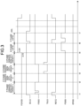
- FIG. 3 is a diagram illustrating an example of operation of the pixel. An example of a timing chart when pixel signals are read is illustrated.
- the power supply voltage FCVDD is controlled to either 2.4 V or 3.3 V. Although the power supply voltage FCVDD may be constant, the lower the power supply voltage FCVDD, the higher the possibility that a dark current can be suppressed. Therefore, in this example, the power supply voltage FCVDD is controlled to 3.3 V only after a LOFIC period described later.
- Each gate electrode (such as gate electrode SELG) is controlled to either a low voltage for turning off the corresponding transistor or a high voltage for turning on the transistor.
- a period from time t2 to time t3 is a period in which the conversion efficiency is high (conversion efficiency H), the gate electrode FDGG has a low voltage, and the transistor FDG is turned off.
- the pixel signal in a state where the capacitance of the floating diffusion FD is not expanded is sent to the column signal processor 6 via the signal line VL.
- a period from time t3 to time t5 is a period in which the pixel signal corresponding to the charge accumulated in the photoelectric conversion element PD is read out. This period is also referred to as a D-phase (data phase) period.
- a period from time t3 to time t4 is a period in which the conversion efficiency is high (conversion efficiency H), and in a state where the gate electrode FDGG is maintained at a low voltage, the gate electrode TGLG has a high voltage.
- the charge accumulated in the photoelectric conversion element PD is transferred to the floating diffusion FD, and the pixel signal is sent to the column signal processor 6 via the signal line VL.
- a period from time t4 to time t5 is a period in which the conversion efficiency is low (conversion efficiency L), and in a state in which the gate electrode FDGG is maintained at a high voltage, the gate electrode TGLG has a high voltage.
- the charge accumulated in the photoelectric conversion element PD is transferred to the floating diffusion FD, and the pixel signal is sent to the column signal processor 6 via the signal line VL.
- the plurality of pixels 2 operate by controlling the voltages of the gate electrodes of the various transistors.
- the isolator 4 may include, for example, a single-layer film or a multi-layer film of an insulator such as silicon oxide (SiO 2 ), tantalum oxide (Ta 2 O 5 ), hafnium oxide (HfO 2 ), or aluminum oxide (Al 2 O 3 ).
- the isolator 4 may include a laminate of a single-layer film or a multilayer film of an insulator such as tantalum oxide, hafnium oxide, or aluminum oxide and a silicon oxide film.
- the isolator 4 may have a gap inside.
- the isolator 4 may include a metal having a high light shielding property, such as tantalum (Ta), aluminum (Al), silver (Ag), gold (Au), or copper (Cu).
- Polysilicon polycrystalline silicon
- the gate electrodes of specific transistors of the plurality of transistors of each of the adjacent pixels 2 are disposed opposite to each other across the isolator 4, and are connected to each other beyond the isolator 4.
- the gate electrode FDGG of the transistor FDG, the gate electrode RSTG of the transistor RST, and the gate electrode SELG of the transistor SEL are gate electrodes of specific transistors.
- the gates of such specific transistors are connected by, for example, a metal wire extending in the X-axis direction (horizontal direction), and thus can be connected to each other beyond the isolator 4.
- the gate electrodes of the transistors other than the specific transistors are disposed in a region other than a region between the gate electrodes of the specific transistors of the adjacent pixels 2.
- the gate electrode TGLG of the transistor TGL, the gate electrode FCGG of the transistor FCG, the gate electrode OFGG of the transistor OFG, and the gate electrode AMPG of the transistor AMP are gate electrodes of transistors other than the specific transistors.
- the gate electrode TGLG, the gate electrode FCGG, the gate electrode OFGG, and the gate electrode AMPG are disposed in a region other than a region between the gate electrodes FDGG of the adjacent pixels 2, a region other than a region between the gate electrodes RSTG, and a region other than a region between the gate electrodes SELG.
- the gate electrodes of the transistors of each of the adjacent pixels 2 are arranged symmetrically with respect to each other across the isolator 4.
- This arrangement can also be referred to as a mirror arrangement in the X-axis direction (mirror arrangement across the Y-axis). It is possible to facilitate layout design and the like.
- the gate electrode not only the gate electrode but also the transistor itself and elements of other circuits may be arranged symmetrically.
- another pattern (not illustrated), for example, a ground pattern or the like may also be provided.
- Each portion of the gate electrode SELG is also referred to as a first portion P1, a second portion P2, and a third portion P3 in the drawing. These portions are similar to the corresponding portions of the gate electrode FDGG described above.
- FIG. 6 schematically illustrates a cross section of a portion including the gate electrode RSTG.
- Each portion of the gate electrode RST is also referred to as a first portion P1, a second portion P2, and a third portion P3 in the drawing. These portions are also similar to the corresponding portions of the gate electrode FDGG described above.
- the gate electrode of the specific transistor shared between the adjacent pixels 2 does not need to be disposed apart from the photodetection element 3. Accordingly, the layout efficiency can be improved. For example, by increasing the area of the gate electrode, the operation can be stabilized and the transfer performance can be improved. The signal saturation can be also suppressed. In the electronic apparatus 100 including the photodetection element 3, advantages such as miniaturization and high performance can be obtained.
- FIGS. 7 and 8 are diagrams illustrating a second configuration example of the photodetection element.
- Several pixels 2 arranged in a Bayer array are exemplified. In this example, it is assumed that the pixel signals of the pixels 2 corresponding to the same color (red, green, or the like) are read together by skipping one row.
- FIG. 7 schematically illustrates a planar layout of each electrode.
- FIG. 8 schematically illustrates a cross section taken along line VIII-VIII in FIG. 7 .
- FIG. 8 schematically illustrates a cross section of a portion including the gate electrode OFGG beyond the isolator 4.
- Each portion of the gate electrode OFGG is also referred to as a first portion P1, a second portion P2, and a third portion P3 in the drawing.
- the first portion P1 of the gate electrode OFGG is a portion located in one pixel of the pixels 2 adjacent in the Y-axis direction (in this example, the pixel 2 on a Y-axis negative direction side).
- the second portion P2 is a portion located in the other pixel (in this example, the pixel 2 on a Y-axis positive direction side).
- the third portion P3 is a portion located on the isolator 4 and connected between the first portion P1 and the second portion P2.
- FIGS. 9 and 10 are diagrams illustrating a third configuration example of the photodetection element.
- the arrangement of the pixel is similar to the arrangement in FIGS. 7 and 8 described above.
- the gate electrodes RSTG of the pixels 2 adjacent in the Y-axis direction are also shared. This is because it is possible to perform reset at the same timing for simultaneous reading.
- FIG. 9 schematically illustrates a planar layout of each electrode.
- FIG. 10 schematically illustrates a cross section taken along line X-X in FIG. 9 .
- FIG. 10 schematically illustrates a cross section of a portion including the gate electrode RSTG beyond the isolator 4 in the Y-axis direction.
- Each portion of the gate electrode RSTG is also referred to as a first portion P1, a second portion P2, and a third portion P3 in the drawing. These portions are similar to the corresponding portions of the gate electrode OFGG ( FIG. 8 ) described above.
- control line HL_RST ( FIG. 2 ) connected to the gate electrode RSTG of each pixel 2 adjacent in the Y-axis direction can be also made common.
- the number of control lines HL can be reduced, and the degree of freedom of wiring can be improved.
- FIGS. 11 and 12 are diagrams illustrating a fourth configuration example of the photodetection element.
- FIG. 11 illustrates an example of a circuit of the pixel 2.
- FIG. 12 schematically illustrates a planar layout of each electrode.
- the transistor FDG is connected between the floating diffusion FD and the transistor RST and the transistor FCG. (The node of) the power supply voltage connected to the transistor RST is referred to as a power supply voltage VDD1 in the drawing.
- the transistor AMP is connected between a power supply voltage VDD2 different from the power supply voltage VDD1 and the signal line VL.
- the power supply voltage VDD1 is controlled to be switchable between a high voltage and a low voltage.
- the transistor AMP can have the function of the transistor SEL described above.
- the power supply voltage VDD1 is switched between a high voltage and a low voltage by a control signal of the transistor SEL. Since the pixel 2 does not include the transistor SEL, the circuit configuration is simplified, and advantages such as improvement in the layout efficiency can be obtained.
- the imaging sections 12101, 12102, 12103, 12104, and 12105 are, for example, disposed at positions on a front nose, sideview mirrors, a rear bumper, and a back door of the vehicle 12100 as well as a position on an upper portion of a windshield within the interior of the vehicle.
- the imaging section 12101 provided to the front nose and the imaging section 12105 provided to the upper portion of the windshield within the interior of the vehicle obtain mainly an image of the front of the vehicle 12100.
- the imaging sections 12102 and 12103 provided to the sideview mirrors obtain mainly an image of the sides of the vehicle 12100.
- the imaging section 12104 provided to the rear bumper or the back door obtains mainly an image of the rear of the vehicle 12100.
- the imaging section 12105 provided to the upper portion of the windshield within the interior of the vehicle is used mainly to detect a preceding vehicle, a pedestrian, an obstacle, a signal, a traffic sign, a lane, or the like.
- FIG. 20 depicts an example of photographing ranges of the imaging sections 12101 to 12104.
- An imaging range 12111 represents the imaging range of the imaging section 12101 provided to the front nose.
- Imaging ranges 12112 and 12113 respectively represent the imaging ranges of the imaging sections 12102 and 12103 provided to the sideview mirrors.
- An imaging range 12114 represents the imaging range of the imaging section 12104 provided to the rear bumper or the back door.
- a bird's-eye image of the vehicle 12100 as viewed from above is obtained by superimposing image data imaged by the imaging sections 12101 to 12104, for example.
- At least one of the imaging sections 12101 to 12104 may have a function of obtaining distance information.
- at least one of the imaging sections 12101 to 12104 may be a stereo camera constituted of a plurality of imaging elements, or may be an imaging element having pixels for phase difference detection.
- the microcomputer 12051 can determine a distance to each three-dimensional object within the imaging ranges 12111 to 12114 and a temporal change in the distance (relative speed with respect to the vehicle 12100) on the basis of the distance information obtained from the imaging sections 12101 to 12104, and thereby extract, as a preceding vehicle, a nearest three-dimensional object in particular that is present on a traveling path of the vehicle 12100 and which travels in substantially the same direction as the vehicle 12100 at a predetermined speed (for example, equal to or more than 0 km/hour). Further, the microcomputer 12051 can set a following distance to be maintained in front of a preceding vehicle in advance, and perform automatic brake control (including following stop control), automatic acceleration control (including following start control), or the like. It is thus possible to perform cooperative control intended for automated driving that makes the vehicle travel automatedly without depending on the operation of the driver or the like.
- automatic brake control including following stop control
- automatic acceleration control including following start control
- the microcomputer 12051 In a situation in which the collision risk is equal to or higher than a set value and there is thus a possibility of collision, the microcomputer 12051 outputs a warning to the driver via the audio speaker 12061 or the display section 12062, and performs forced deceleration or avoidance steering via the driving system control unit 12010. The microcomputer 12051 can thereby assist in driving to avoid collision.
- the sound/image output section 12052 controls the display section 12062 so that a square contour line for emphasis is displayed so as to be superimposed on the recognized pedestrian.
- the sound/image output section 12052 may also control the display section 12062 so that an icon or the like representing the pedestrian is displayed at a desired position.
- the technology according to an embodiment of the present disclosure can be applied to, for example, the imaging section 12031 and the like among the configurations described above.
- By applying the technology according to an embodiment of the present disclosure to the imaging section 12031 and the like it is possible to reduce the size, improve the performance, and the like of the imaging section 12031.
Landscapes
- Engineering & Computer Science (AREA)
- Multimedia (AREA)
- Signal Processing (AREA)
- Solid State Image Pick-Up Elements (AREA)
- Transforming Light Signals Into Electric Signals (AREA)
Abstract
Description
- The present disclosure relates to a photodetection element and an electronic apparatus.
- For example, Patent Literature 1 discloses an imaging device including an isolator that isolates adjacent pixels from each other.
- Patent Literature 1:
JP 2020-194912 A - The presence of the isolator restricts an arrangement of a photoelectric conversion element and a transistor in the pixel and reduces layout efficiency.
- One aspect of the present disclosure improves layout efficiency.
- A photodetection element according to one aspect of the present disclosure includes: a plurality of pixels disposed in a planar direction; and an isolator that extends in a direction intersecting the planar direction between adjacent pixels of the plurality of pixels so as to isolate the adjacent pixels from each other, wherein each of the plurality of pixels includes a photoelectric conversion element, and a plurality of transistors, and gate electrodes of specific transistors of the plurality of transistors of each of the adjacent pixels are arranged opposite to each other across the isolator and are connected to each other beyond the isolator in plan view.
- An electronic apparatus according to one aspect of the present disclosure includes a photodetection element, wherein the photodetection element includes a plurality of pixels disposed in a planar direction, and an isolator that extends in a direction intersecting the planar direction between adjacent pixels of the plurality of pixels so as to isolate the adjacent pixels from each other, each of the plurality of pixels includes a photoelectric conversion element, and a plurality of transistors, and gate electrodes of specific transistors of the plurality of transistors of each of the adjacent pixels are arranged opposite to each other across the isolator and are connected to each other beyond the isolator in plan view.
-
-
FIG. 1 is a diagram illustrating an example of a schematic configuration of an electronic apparatus including a photodetection element according to an embodiment. -
FIG. 2 is a circuit diagram illustrating an example of a schematic configuration of a pixel. -
FIG. 3 is a diagram illustrating an example of operation of the pixel. -
FIG. 4 is a diagram illustrating a first configuration example of the photodetection element. -
FIG. 5 is a diagram illustrating the first configuration example of the photodetection element. -
FIG. 6 is a diagram illustrating the first configuration example of the photodetection element. -
FIG. 7 is a diagram illustrating a second configuration example of the photodetection element. -
FIG. 8 is a diagram illustrating the second configuration example of the photodetection element. -
FIG. 9 is a diagram illustrating a third configuration example of the photodetection element. -
FIG. 10 is a diagram illustrating the third configuration example of the photodetection element. -
FIG. 11 is a diagram illustrating a fourth configuration example of the photodetection element. -
FIG. 12 is a diagram illustrating the fourth configuration example of the photodetection element. -
FIG. 13 is a diagram illustrating a fifth configuration example of the photodetection element. -
FIG. 14 is a diagram illustrating the fifth configuration example of the photodetection element. -
FIG. 15 is a diagram illustrating a sixth configuration example of the photodetection element. -
FIG. 16 is a diagram illustrating the sixth configuration example of the photodetection element. -
FIG. 17 is a diagram illustrating a seventh configuration example of the photodetection element. -
FIG. 18 is a diagram illustrating the seventh configuration example of the photodetection element. -
FIG. 19 is a block diagram depicting an example of schematic configuration of a vehicle control system. -
FIG. 20 is a diagram of assistance in explaining an example of installation positions of an outside-vehicle information detecting section and an imaging section. Description of Embodiments - Hereinafter, embodiments of the present disclosure will be described in detail with reference to the drawings. Note that, in the following embodiments, the same elements are denoted by the same reference signs, and redundant description will be omitted.
- The present disclosure will be described in accordance with the following order of items.
- 0. Introduction
- 1. Embodiments
- 1.1 First configuration example
- 1.2 Second configuration example
- 1.3 Third configuration example
- 1.4 Fourth configuration example
- 1.5 Fifth configuration example
- 1.6 Sixth configuration example
- 1.7 Seventh configuration example
- 2. Examples of effects
- 3. Application examples to mobile body
- As a device including a photodetection element and an electronic apparatus, a CMOS image sensor (CMOS type solid-state imaging device) and the like are known. A miniaturization technology associated with a CMOS process facilitates creation of an active structure having an amplification function for every pixel. In addition, a peripheral circuit unit such as a signal processing circuit that processes a signal output from each pixel of a pixel array unit can be integrated on the same chip (substrate) as the pixel array unit. Many technologies related to CMOS image sensors have been proposed.
- For example, various technologies for expanding a dynamic range have been proposed. In a technology also referred to as lateral overflow integration capacitor (LOFIC) or the like, a capacitor is provided in a pixel to directly increase the amount of charge handled. There is also a technology in which large and small photoelectric conversion elements having different light receiving sensitivities are included in one pixel. There is also known a technology of a global shutter system in which exposure of all pixels is simultaneously started and exposure of all pixels is simultaneously ended as disclosed in Patent Literature 1. As the technology advances, a pixel architecture becomes complicated, and the number of elements such as transistors in the pixel has also increased.
- In recent years, a deep insulator such as deep trench isolation (DTI) is often provided as an isolator for isolating elements between pixels. The presence of the isolator surrounding a pixel restricts an arrangement of a photoelectric conversion element and a transistor and reduces layout efficiency. A gate electrode is disposed apart from the isolator in order to avoid a short circuit risk. As a result, the size of the transistor becomes smaller, and the like, and a decrease in a saturation signal amount, a transfer failure, and the like can occur. Such a problem becomes more apparent due to an increase in the number of elements such as transistors accompanying miniaturization and high functionality of pixels.
- At least some of the problems as described above are addressed by the disclosed technology. The elements of each of the adjacent pixels are arranged, for example, symmetrically across the isolator. The transistors located near the isolator of the transistors of the adjacent pixels share the gate electrode. Accordingly, an unnecessary space is eliminated, and the layout efficiency is improved.
-
FIG. 1 is a diagram illustrating an example of a schematic configuration of an electronic apparatus including a photodetection element according to an embodiment. An illustratedelectronic apparatus 100 is a CMOS image sensor and includes a pixel array unit 1 and a peripheral unit. These elements are formed, for example, on a semiconductor substrate of silicon or the like. As the peripheral unit,FIG. 1 illustrates avertical drive unit 5, acolumn signal processor 6, a horizontal drive unit 7, asignal processor 8, and asystem controller 9. -
FIG. 1 also illustrates an XYZ coordinate system for the pixel array unit 1. An X-axis direction is also referred to as a horizontal direction (lateral direction) or the like. A Y-axis direction is also referred to as a vertical direction (longitudinal direction) or the like. A Z-axis direction is a direction orthogonal to an XY plane direction, and corresponds to, for example, a thickness direction of the semiconductor substrate. - The pixel array unit 1 includes a plurality of
pixels 2. The plurality ofpixels 2 is two-dimensionally arranged in the X-axis direction and the Y-axis direction. Eachpixel 2 generates and outputs a voltage signal corresponding to the amount of received light. This signal is also referred to as a pixel signal. - At least some of the plurality of
pixels 2 constitute aphotodetection element 3. Thephotodetection element 3 includes at least two adjacent pixels of the plurality ofpixels 2. Thephotodetection element 3 and the plurality ofpixels 2 may be appropriately read as long as there is no contradiction. - The
vertical drive unit 5 drives the plurality ofpixels 2 of the pixel array unit 1, for example, all at the same time or for every pixel row. The driving includes selective scanning or the like of the plurality ofpixels 2 row by row in order to read the pixel signal. The pixel signal of the selectively scannedpixel 2 is sent to thecolumn signal processor 6. - The
vertical drive unit 5 is connected to the pixel array unit 1 via a plurality of control lines HL for every pixel row, for example. Each control line HL extends in a row direction and connects eachpixel 2 of the corresponding pixel row and thevertical drive unit 5. Thevertical drive unit 5 includes, for example, a shift register, an address decoder, and the like. - In the present disclosure, being connected may be understood as being electrically connected. Being electrically connected may include being connected with another element interposed therebetween as long as the functions of the connected elements are not hindered.
- The
column signal processor 6 processes the pixel signal from eachpixel 2 in the row selected by thevertical drive unit 5 for every pixel column. For example, thecolumn signal processor 6 includes a plurality of unit circuits corresponding to the pixel columns. The processing by thecolumn signal processor 6 includes noise removal processing, correlated double sampling (CDS) processing, double data sampling (DDS) processing, analog/digital (A/D) conversion processing of analog pixel signals, and the like. The pixel signal is digitized and sent to thesignal processor 8. - The
column signal processor 6 is connected to the pixel array unit 1 via a plurality of signal lines VL. Each signal line VL extends in a column direction and connects eachpixel 2 of the corresponding pixel column and thecolumn signal processor 6. Thecolumn signal processor 6 includes, for example, a shift register, an address decoder, and the like. - The horizontal drive unit 7 sequentially selects the unit circuits of the
column signal processor 6. By being selectively scanned by the horizontal drive unit 7, the pixel signals for every pixel column processed by thecolumn signal processor 6 is sequentially output to thesignal processor 8. The horizontal drive unit 7 includes, for example, a shift register, an address decoder, and the like. - The
signal processor 8 processes the pixel signal from thecolumn signal processor 6, and generates and outputs an image signal based on the pixel signal. Note that data and the like most necessary for the processing can be temporarily stored in, for example, a storage (not illustrated). - The
system controller 9 controls thevertical drive unit 5, thecolumn signal processor 6, and the horizontal drive unit 7. For example, thesystem controller 9 includes a timing generator or the like so as to generate various timing signals and supply the timing signals to corresponding portions. - The
pixel 2 of the pixel array unit 1 will be described with reference toFIG. 2 . -
FIG. 2 is a circuit diagram illustrating an example of a schematic configuration of a pixel. In this example, thepixel 2 includes a photoelectric conversion element PD, a floating diffusion FD, a capacitor FC, and a plurality of transistors. Examples of the plurality of transistors include a transistor TGL, a transistor FDG, a transistor FCG, a transistor OFG, a transistor RST, a transistor AMP, and a transistor SEL. - The exemplified transistor is an FET, and has a drain and a source which are current terminals, and a gate electrode which is a control terminal. Unless otherwise stated, connecting a transistor between two elements means that one current terminal (drain or source) of the transistor is connected to one element and the other current terminal of the transistor is connected to the other element.
- The gate electrode of the transistor TGL is referred to as a gate electrode TGLG in the drawing. The gate electrode of the transistor FDG is referred to as a gate electrode FDGG in the drawing. The gate electrode of the transistor FCG is referred to as a gate electrode FCGG in the drawing. The gate electrode of the transistor OFG is referred to as a gate electrode OFGG in the drawing. The gate electrode of the transistor RST is referred to as a gate electrode RSTG in the drawing. The gate electrode of the transistor AMP is referred to as a gate electrode AMPG in the drawing. The gate electrode of the transistor SEL is referred to as a gate electrode SELG in the drawing. The gate of the transistor AMP is connected to the floating diffusion FD.
- Of the plurality of control lines HL connected to one
pixel 2, the control line HL connected to the gate electrode TGLG of the transistor TGL is referred to as a control line HL_TGL in the drawing. The control line HL connected to the gate electrode FDGG of the transistor FDG is referred to as a control line HL_FDG in the drawing. The control line HL connected to the gate electrode FCGG of the transistor FCG is referred to as a control line HL_FCG in the drawing. The control line HL connected to the gate electrode OFGG of the transistor OFG is referred to as a control line HL_OFG in the drawing. The control line HL connected to the gate electrode RSTG of the transistor RST is referred to as a control line HL_RST in the drawing. The control line HL connected to the gate electrode SELG of the transistor SEL is referred to as a control line HL_SEL in the drawing. The ON/OFF state (conductive state or non-conductive state) of each transistor is controlled by a control signal from the corresponding control line HL. - The photoelectric conversion element PD generates and accumulates charge corresponding to the amount of received light. An example of the photoelectric conversion element PD is a photodiode or the like.
- The transistor TGL is a transfer transistor for transferring the charge of the photoelectric conversion element PD to the floating diffusion FD. The transistor TGL is connected between the photoelectric conversion element PD and the floating diffusion FD.
- The floating diffusion FD accumulates the charge from the photoelectric conversion element PD transferred via the transfer transistor TGL and converts the charge into a voltage. A voltage corresponding to the amount of the accumulated charge is generated. The floating diffusion FD is formed to have a floating diffusion capacitance at least between the transistor TGL, the transistor AMP, and the transistor FDG.
- The transistor FDG is a conversion efficiency switching transistor that switches conversion efficiency from charge to voltage in the floating diffusion FD. The transistor FDG is connected between the floating diffusion FD and the transistor RST and the transistor FCG. When the transistor FDG is turned on, the region of the floating diffusion FD spreads to a region opposite to the floating diffusion FD across the FDG, and the capacitance of the floating diffusion FD increases accordingly. When the capacitance of the floating diffusion FD increases, the voltage change to the change in the amount of accumulated charge becomes gentle accordingly, and the conversion efficiency decreases. Conversely, when the transistor FDG is turned off, the capacitance of the floating diffusion FD decreases, and the conversion efficiency increases accordingly.
- The transistor FCG is a capacitive connection transistor for connecting the capacitor FC to the floating diffusion FD. The transistor FCG is connected between the transistor FDG and the transistor RST, and the capacitor FC and the transistor OFG.
- The transistor OFG is an overflow transistor (overflow gate) for transferring charge overflowed from the photoelectric conversion element PD to the capacitor FC. The transistor OFG is connected between the photoelectric conversion element PD and the capacitor FC and the transistor FCG.
- The capacitor FC is used to accumulate the charge overflowing from the photoelectric conversion element PD. The capacitor FC is connected between (the node of) a power supply voltage FCVDD and the transistor OFG and the transistor FCG. The capacitor FC has, for example, a metal-insulator-metal (MIM) structure, and the capacitor FC in that case is an MIM capacitor.
- The transistor RST is a reset transistor for discharging the charge accumulated in the floating diffusion FD. The transistor RST is connected between (the node of) a power supply voltage VDD and the transistor FDG and the transistor FCG.
- The transistor AMP is an amplifier transistor that outputs a voltage signal corresponding to the voltage of the floating diffusion FD. The transistor AMP is connected between the power supply voltage VDD and the transistor SEL. The voltage signal output from the transistor AMP can correspond to a pixel signal.
- The transistor SEL is a selection transistor for selectively outputting the voltage signal output from the transistor AMP to the signal line VL. The transistor SEL is connected between the transistor AMP and the signal line VL.
- An example of operation of the
pixel 2 having the above configuration will be described with reference toFIG. 3 . -
FIG. 3 is a diagram illustrating an example of operation of the pixel. An example of a timing chart when pixel signals are read is illustrated. The power supply voltage FCVDD is controlled to either 2.4 V or 3.3 V. Although the power supply voltage FCVDD may be constant, the lower the power supply voltage FCVDD, the higher the possibility that a dark current can be suppressed. Therefore, in this example, the power supply voltage FCVDD is controlled to 3.3 V only after a LOFIC period described later. Each gate electrode (such as gate electrode SELG) is controlled to either a low voltage for turning off the corresponding transistor or a high voltage for turning on the transistor. - A period from time t1 to time t3 is a period in which a pixel signal (reset voltage signal) when the floating diffusion FD is reset is read. This period is also referred to as a P-phase (precharge phase) period. The gate electrode SELG is maintained at a high voltage. The gate electrode RSTG and the gate electrode FDGG have a high voltage, and the floating diffusion FD is reset. A period from time t1 to time t2 is a period in which the conversion efficiency is low (conversion efficiency L), and the gate electrode FDGG has a high voltage, that is, the transistor FDG is turned on. The pixel signal in a state where the capacitance of the floating diffusion FD is expanded is sent to the
column signal processor 6 via the signal line VL. A period from time t2 to time t3 is a period in which the conversion efficiency is high (conversion efficiency H), the gate electrode FDGG has a low voltage, and the transistor FDG is turned off. The pixel signal in a state where the capacitance of the floating diffusion FD is not expanded is sent to thecolumn signal processor 6 via the signal line VL. - A period from time t3 to time t5 is a period in which the pixel signal corresponding to the charge accumulated in the photoelectric conversion element PD is read out. This period is also referred to as a D-phase (data phase) period. A period from time t3 to time t4 is a period in which the conversion efficiency is high (conversion efficiency H), and in a state where the gate electrode FDGG is maintained at a low voltage, the gate electrode TGLG has a high voltage. The charge accumulated in the photoelectric conversion element PD is transferred to the floating diffusion FD, and the pixel signal is sent to the
column signal processor 6 via the signal line VL. A period from time t4 to time t5 is a period in which the conversion efficiency is low (conversion efficiency L), and in a state in which the gate electrode FDGG is maintained at a high voltage, the gate electrode TGLG has a high voltage. The charge accumulated in the photoelectric conversion element PD is transferred to the floating diffusion FD, and the pixel signal is sent to thecolumn signal processor 6 via the signal line VL. - By the CDS processing of the
column signal processor 6 described above, reset noise and the like are removed on the basis of the pixel signal read in the P-phase period and the pixel signal read in the D-phase period. - A period from time t5 to time t7 is a period in which the pixel signal is read by using the capacitor FC. This period is also referred to as a lateral overflow integration capacitor (LOFIC) period. In a state where the gate electrode FDGG is maintained at a high voltage, the gate electrode FCGG also has a high voltage. Not only the transistor FDG but also the transistor FCG is turned on. In a state where the capacitor FC is connected to the floating diffusion FD, the pixel signal is sent to the
column signal processor 6 via the signal line VL. A period from time t5 to time t6 is a D-phase period, and a period from time t6 to time t7 is a P-phase period. At the beginning of the P-phase period, the gate electrode RSTG has a high voltage, and the floating diffusion FD is reset. On the pixel signal in the LOFIC period, for example, the DDS processing of thecolumn signal processor 6 described above is executed. - In the example illustrated in
FIG. 3 , a short period after time t7 is provided as a digital overlap (DOL) period. The voltage of the gate electrode SELG is maintained at a high voltage only during the period, and the pixel signal is extracted via the signal line VL. It is also possible to cope with a case where the amount of received light is extremely large. - For example, as described above, the plurality of
pixels 2 operate by controlling the voltages of the gate electrodes of the various transistors. - In the present embodiment, the layout efficiency is improved by make some gate electrodes common. Some examples of specific configurations will be described with reference to
FIG. 4 and subsequent drawings. -
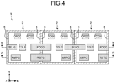
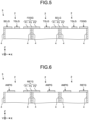
FIGS. 4 to 6 are diagrams illustrating a first configuration example of the photodetection element. Threepixels 2 arranged side by side in the X-axis direction are exemplified.FIG. 4 schematically illustrates a planar layout of each electrode.FIG. 5 schematically illustrates a cross section taken along line V-V inFIG. 4 .FIG. 6 schematically illustrates a cross section taken along line VI-VI inFIG. 4 . In the following description, a plan view means that thephotodetection element 3, that is, the plurality ofpixels 2 is viewed in a plan view (viewed in the Z-axis direction). - The
photodetection element 3 includes anisolator 4. Theisolator 4 isolates theadjacent pixels 2 from each other. The isolation by theisolator 4 includes at least one of electrical isolation or optical isolation. In this example, theisolator 4 is provided so as to surround eachpixel 2 in plan view (when viewed in the Z-axis direction). Theisolator 4 extends between theadjacent pixels 2 in a direction intersecting the XY plane direction, in this example, the Z-axis direction. Theisolator 4 can also be said to be a wall that partitions theadjacent pixels 2. Each element of onepixel 2, for example, the photoelectric conversion element PD, the floating diffusion FD, various transistors, the capacitor FC, and the like described above are formed in one region partitioned by theisolator 4. - The
isolator 4 may include, for example, a single-layer film or a multi-layer film of an insulator such as silicon oxide (SiO2), tantalum oxide (Ta2O5), hafnium oxide (HfO2), or aluminum oxide (Al2O3). Theisolator 4 may include a laminate of a single-layer film or a multilayer film of an insulator such as tantalum oxide, hafnium oxide, or aluminum oxide and a silicon oxide film. Theisolator 4 may have a gap inside. Theisolator 4 may include a metal having a high light shielding property, such as tantalum (Ta), aluminum (Al), silver (Ag), gold (Au), or copper (Cu). Polysilicon (polycrystalline silicon) may be used as a material of theisolator 4. - In the present embodiment, in plan view, the gate electrodes of specific transistors of the plurality of transistors of each of the
adjacent pixels 2 are disposed opposite to each other across theisolator 4, and are connected to each other beyond theisolator 4. Specifically, in the example illustrated inFIG. 4 , the gate electrode FDGG of the transistor FDG, the gate electrode RSTG of the transistor RST, and the gate electrode SELG of the transistor SEL are gate electrodes of specific transistors. The gates of such specific transistors are connected by, for example, a metal wire extending in the X-axis direction (horizontal direction), and thus can be connected to each other beyond theisolator 4. - The gate electrodes of the transistors other than the specific transistors are disposed in a region other than a region between the gate electrodes of the specific transistors of the
adjacent pixels 2. Specifically, in the example illustrated inFIG. 4 , the gate electrode TGLG of the transistor TGL, the gate electrode FCGG of the transistor FCG, the gate electrode OFGG of the transistor OFG, and the gate electrode AMPG of the transistor AMP are gate electrodes of transistors other than the specific transistors. The gate electrode TGLG, the gate electrode FCGG, the gate electrode OFGG, and the gate electrode AMPG are disposed in a region other than a region between the gate electrodes FDGG of theadjacent pixels 2, a region other than a region between the gate electrodes RSTG, and a region other than a region between the gate electrodes SELG. - In the example illustrated in
FIG. 4 , the gate electrodes of the transistors of each of theadjacent pixels 2 are arranged symmetrically with respect to each other across theisolator 4. This arrangement can also be referred to as a mirror arrangement in the X-axis direction (mirror arrangement across the Y-axis). It is possible to facilitate layout design and the like. Not only the gate electrode but also the transistor itself and elements of other circuits may be arranged symmetrically. Note that another pattern (not illustrated), for example, a ground pattern or the like may also be provided. -
FIG. 5 schematically illustrates a cross section of a portion including the gate electrode FDGG and the gate electrode SELG beyond theisolator 4. Elements other than theisolator 4 and the gate electrode are not illustrated. The same applies to other sectional views. - The gate electrode FDGG includes a first portion P1, a second portion P2, and a third portion P3. The first portion P1 of the gate electrode FDGG is a portion located in one pixel of the
pixels 2 adjacent in the X-axis direction (in this example, thepixel 2 on an X-axis negative direction side). The second portion P2 is a portion located in the other pixel (in this example, thepixel 2 on an X-axis positive direction side). The third portion P3 is a portion located on theisolator 4 and connected between the first portion P1 and the second portion P2. - Each portion of the gate electrode SELG is also referred to as a first portion P1, a second portion P2, and a third portion P3 in the drawing. These portions are similar to the corresponding portions of the gate electrode FDGG described above.
-
FIG. 6 schematically illustrates a cross section of a portion including the gate electrode RSTG. Each portion of the gate electrode RST is also referred to as a first portion P1, a second portion P2, and a third portion P3 in the drawing. These portions are also similar to the corresponding portions of the gate electrode FDGG described above. - In the
photodetection element 3 having the configuration described above, the gate electrode of the specific transistor shared between theadjacent pixels 2 does not need to be disposed apart from thephotodetection element 3. Accordingly, the layout efficiency can be improved. For example, by increasing the area of the gate electrode, the operation can be stabilized and the transfer performance can be improved. The signal saturation can be also suppressed. In theelectronic apparatus 100 including thephotodetection element 3, advantages such as miniaturization and high performance can be obtained. -
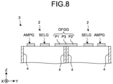
FIGS. 7 and8 are diagrams illustrating a second configuration example of the photodetection element.Several pixels 2 arranged in a Bayer array are exemplified. In this example, it is assumed that the pixel signals of thepixels 2 corresponding to the same color (red, green, or the like) are read together by skipping one row.FIG. 7 schematically illustrates a planar layout of each electrode.FIG. 8 schematically illustrates a cross section taken along line VIII-VIII inFIG. 7 . - In this example, the transistor OFG of the transistor OFG is also a gate electrode of a specific transistor. Specifically, the gate electrodes OFGG of the transistors OFG of the
pixels 2 adjacent in the Y-axis direction are disposed opposite to each other across theisolator 4, and are connected to each other beyond theisolator 4. The gate electrode TGLG of the transistor TGL, the gate electrode FCGG of the transistor FCG, and the gate electrode AMPG of the transistor AMP are gate electrodes of transistors other than the specific transistors. The gate electrode TGLG, the gate electrode FCGG, and the gate electrode AMPG are disposed in a region other than a region between the gate electrodes FDGG of theadjacent pixels 2, a region other than a region between the gate electrodes RSTG, a region other than a region between the gate electrodes SELG, and a region other than a region between the gate electrodes OFGG. The gate electrodes of the transistors of each of thepixels 2 adjacent in the Y-axis direction may be arranged symmetrically with respect to each other across the isolator 4 (mirror arrangement across the X-axis in the Y-axis direction). -
FIG. 8 schematically illustrates a cross section of a portion including the gate electrode OFGG beyond theisolator 4. Each portion of the gate electrode OFGG is also referred to as a first portion P1, a second portion P2, and a third portion P3 in the drawing. The first portion P1 of the gate electrode OFGG is a portion located in one pixel of thepixels 2 adjacent in the Y-axis direction (in this example, thepixel 2 on a Y-axis negative direction side). The second portion P2 is a portion located in the other pixel (in this example, thepixel 2 on a Y-axis positive direction side). The third portion P3 is a portion located on theisolator 4 and connected between the first portion P1 and the second portion P2. - In the above configuration, the control line HL_OFG (
FIG. 2 ) connected to the gate electrode OFGG of each of thepixels 2 adjacent in the Y-axis direction can also be made common. As a result, the number of control lines HL_OFG for two pixels can be reduced from two to one. By reducing the number of control lines HL, the degree of freedom of a wiring layout is improved. For example, the possibility of improving an RC time constant or reducing a yield reduction due to dust is also increased. The same may apply to the case of simultaneously reading four pixels of the same color. -
FIGS. 9 and10 are diagrams illustrating a third configuration example of the photodetection element. The arrangement of the pixel is similar to the arrangement inFIGS. 7 and8 described above. Here, it is assumed that the pixel signals of thepixels 2 adjacent in the Y-axis direction and corresponding to different colors are read together. In this case, the gate electrodes RSTG of thepixels 2 adjacent in the Y-axis direction are also shared. This is because it is possible to perform reset at the same timing for simultaneous reading.FIG. 9 schematically illustrates a planar layout of each electrode.FIG. 10 schematically illustrates a cross section taken along line X-X inFIG. 9 . -
FIG. 10 schematically illustrates a cross section of a portion including the gate electrode RSTG beyond theisolator 4 in the Y-axis direction. Each portion of the gate electrode RSTG is also referred to as a first portion P1, a second portion P2, and a third portion P3 in the drawing. These portions are similar to the corresponding portions of the gate electrode OFGG (FIG. 8 ) described above. - In the above configuration, the control line HL_RST (
FIG. 2 ) connected to the gate electrode RSTG of eachpixel 2 adjacent in the Y-axis direction can be also made common. As described above, the number of control lines HL can be reduced, and the degree of freedom of wiring can be improved. -
FIGS. 11 and12 are diagrams illustrating a fourth configuration example of the photodetection element.FIG. 11 illustrates an example of a circuit of thepixel 2.FIG. 12 schematically illustrates a planar layout of each electrode. The transistor FDG is connected between the floating diffusion FD and the transistor RST and the transistor FCG. (The node of) the power supply voltage connected to the transistor RST is referred to as a power supply voltage VDD1 in the drawing. The transistor AMP is connected between a power supply voltage VDD2 different from the power supply voltage VDD1 and the signal line VL. - The power supply voltage VDD1 is controlled to be switchable between a high voltage and a low voltage. By controlling the power supply voltage VDD1 to change an input voltage of the transistor AMP, the transistor AMP can have the function of the transistor SEL described above. For example, the power supply voltage VDD1 is switched between a high voltage and a low voltage by a control signal of the transistor SEL. Since the
pixel 2 does not include the transistor SEL, the circuit configuration is simplified, and advantages such as improvement in the layout efficiency can be obtained. - Since there is no transistor SEL, the gate electrode SELG is also excluded from the planar layout. The gate electrode FDGG, the gate electrode FCGG, and the gate electrode OFGG of each of the
pixels 2 adjacent in the X-axis direction are shared. These gate electrodes are connected by, for example, a metal wire extending in the X-axis direction (horizontal direction), and thus can be connected to each other beyond theisolator 4. -
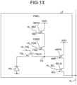
FIGS. 13 and14 are diagrams illustrating a fifth configuration example of the photodetection element.FIG. 13 is a circuit diagram of thepixel 2. The exemplifiedpixel 2 is different from the configuration described above in that the transistor FCG, the capacitor FC, and the transistor OFG are not included.FIG. 14 schematically illustrates a planar layout of each electrode. The gate electrode FDGG, the gate electrode RSTG, and the gate electrode SELG are gate electrodes of a specific transistor. The gate electrodes FDGG of thepixels 2 adjacent in the X-axis direction are disposed opposite to each other across theisolator 4, and are connected to each other beyond theisolator 4. The same applies to the gate electrode RSTG and the gate electrode SELG. -
FIGS. 15 and16 are diagrams illustrating a sixth configuration example of the photodetection element.FIG. 15 is a circuit diagram of thepixel 2. The exemplifiedpixel 2 is different from the configuration inFIG. 13 in that thepixel 2 does not include the transistor FDG.FIG. 16 schematically illustrates a planar layout of each electrode. The gate electrode RSTG and the gate electrode SELG are gate electrodes of a specific transistor. -
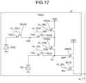
FIGS. 17 and18 are diagrams illustrating a seventh configuration example of the photodetection element.FIG. 17 is a circuit diagram of thepixel 2. The exemplifiedpixel 2 further includes a photoelectric conversion element PD2, a transistor TGL2, and a floating diffusion FD2 as compared with the configuration inFIG. 2 described above. The transistor TGL2 is a second transfer transistor for transferring the charge of the photoelectric conversion element PD2 to the floating diffusion FD2. The transistor FCG is connected between the floating diffusion FD2 and the transistor RST and the transistor FDG. The gate electrode of the transistor TGL2 is referred to as a gate electrode TGLG2 in the drawing. The control line HL connected to the gate electrode TGLG2 is referred to as a control line HL_TGL2 in the drawing. - The photoelectric conversion element PD and the photoelectric conversion element PD2 have different light receiving sensitivities. The photoelectric conversion element PD2 is designed to be smaller than the photoelectric conversion element PD, specifically, to have an area smaller than a light receiving area of the photoelectric conversion element PD. It can be said that the
pixel 2 includes a large pixel including the photoelectric conversion element PD and a small pixel including the photoelectric conversion element PD2. By using the two light receiving elements of the photoelectric conversion element PD and the photoelectric conversion element PD2 in combination, it is possible to cope with a wide range of amounts of received light, and it is possible to expand the dynamic range accordingly. - In plan view of the
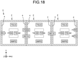
photodetection element 3, the gate electrode of the transistor connected to the photoelectric conversion element PD2 is disposed closer to the center of thepixel 2 than the gate electrode of the transistor connected to the photoelectric conversion element PD.FIG. 18 schematically illustrates a planar layout of each electrode. A region of a central portion of thepixel 2 is indicated by a broken line. The photoelectric conversion element PD2, the gate electrode TGLG2 of the transistor TGL2 connected to the photoelectric conversion element PD2, the floating diffusion FD2, the gate electrode FCGG of the transistor FCG, and the like are disposed inside a region indicated by the broken line. The photoelectric conversion element PD, the gate electrode TGLG of the transistor TGL connected to the photoelectric conversion element PD, the gate electrode FDGG of the transistor FDG, the gate electrode RSTG of the transistor RST, the transistor AMP of the transistor AMP, the gate electrode SELG of the transistor SEL, and the like are disposed outside a region indicated by the broken line. The gate electrode FDGG, the gate electrode RSTG, and the gate electrode SELG are gate electrodes of a specific transistor. - The technology described above is specified as follows, for example. One of the disclosed technologies is a
photodetection element 3. As described with reference toFIGS. 1 to 6 and the like, thephotodetection element 3 includes the plurality ofpixels 2 disposed in the XY plane direction, and theisolator 4 extending in a direction intersecting the XY plane direction (for example, the Z-axis direction) between theadjacent pixels 2 so as to isolate theadjacent pixels 2 of the plurality ofpixels 2. Each of the plurality ofpixels 2 includes a photoelectric conversion element PD and a plurality of transistors. In plan view(when viewed in the Z-axis direction), the gate electrodes of specific transistors of the plurality of transistors of each of theadjacent pixels 2 are disposed opposite to each other across theisolator 4, and are connected to each other beyond theisolator 4. - In the
photodetection element 3, for example, the gate electrode of a specific transistor does not need to be disposed apart from thephotodetection element 3. Accordingly, the layout efficiency can be improved. - As described with reference to
FIGS. 5, 6 , and the like, the gate electrode of the specific transistor includes the first portion P1 located in onepixel 2 of theadjacent pixels 2, the second portion P2 located in theother pixel 2 of theadjacent pixels 2, and the third portion P3 located on theisolator 4 and connected between the first portion P1 and the second portion P2. For example, in this manner, the gate electrodes of the specific transistors of theadjacent pixels 2 can be connected to each other beyond theisolator 4. - As described with reference to
FIGS. 4 to 6 and the like, of the plurality of transistors, the gate electrodes of the transistors other than the specific transistors may be disposed in a region other than a region between the gate electrodes of the specific transistors of theadjacent pixels 2. For example, by arranging the gate electrode of each transistor in this manner, the gate electrode can be made common. - As described with reference to
FIG. 4 and the like, the gate electrodes of the plurality of transistors of each of theadjacent pixels 2 may be arranged symmetrically with respect to each other across theisolator 4 in plan view (when viewed in the Z-axis direction). It is therefore possible to facilitate the layout design and the like. - As described with reference to
FIGS. 2 ,4 to 6 , and the like, theadjacent pixels 2 may include twopixels 2 arranged side by side in the X-axis direction (horizontal direction) which is an extending direction of the control line HL of each of the plurality of transistors. The gate electrode of the specific transistor may include at least one of the gate electrode FDGG of the transistor FDG, the gate electrode RSTG of the transistor RST, the gate electrode SELG of the transistor SEL, or the gate electrode RSTG of the transistor RST. The transistor FDG is a conversion efficiency switching transistor for switching the conversion efficiency of the floating diffusion FD that accumulates the charge generated in the photoelectric conversion element PD and converts the charge into a voltage. The transistor RST is a reset transistor for discharging the charge accumulated in the floating diffusion FD. The transistor SEL is a selection transistor for selectively outputting a voltage signal (pixel signal) corresponding to the charge accumulated in the floating diffusion FD. For example, the gate electrodes of specific transistors of theadjacent pixels 2 can be made common. - As described with reference to
FIGS. 2 ,4 ,6 to 10 , and the like, theadjacent pixels 2 may include twopixels 2 arranged side by side in the Y-axis direction (vertical direction). The gate electrode of the specific transistor may include at least one of the gate electrode RSTG of the transistor RST or the gate electrode OFGG of the transistor OFG. The transistor OFG is an overflow transistor for transferring a charge overflowed in the photoelectric conversion element PD to, for example, the capacitor FD having an MIM structure. For example, the gate electrodes of specific transistors of theadjacent pixels 2 can be made common. In this case, the number of control lines HL_RST connected to the common gate electrode RSTG can be reduced from two to one. Similarly, the number of control lines HL_OFG connected to the common gate electrode OFGG can be reduced from two to one. The layout efficiency can be further improved. - As described with reference to
FIGS. 17 and18 and the like, each of the plurality ofpixels 2 may include the photoelectric conversion element PD2 (second photoelectric conversion element) smaller than the photoelectric conversion element PD, and the gate electrode (the gate electrode TGLG2 of the transistor TGL2 and the like) of the transistor connected to the photoelectric conversion element PD2 of each of the plurality ofpixels 2 may be disposed closer to the center of thepixel 2 than the gate electrode (the gate electrode TGLG of the transistor TGL and the like) of the transistor connected to the photoelectric conversion element PD in plan view (when viewed in the Z-axis direction). For example, in this manner, the photoelectric conversion element PD1 and the photoelectric conversion element PD2 can be used in combination to improve the layout efficiency in the configuration corresponding to expansion of the dynamic range. - The
electronic apparatus 100 including thephotodetection element 3 described with reference toFIG. 1 and the like is also one of the disclosed technologies. By providing thephotodetection element 3 with improved layout efficiency, it is possible to reduce the size and improve the performance of theelectronic apparatus 100. - Note that the effects described in the present disclosure are merely examples and are not limited to the disclosed contents. Other effects may be obtained.
- The technology according to an embodiment of the present disclosure (present technology) can be applied to various products. For example, the technology according to an embodiment of the present disclosure may be implemented as a device mounted on any type of mobile body such as an automobile, an electric vehicle, a hybrid electric vehicle, a motorcycle, a bicycle, a personal mobility, an airplane, a drone, a ship, and a robot.
-
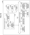
FIG. 19 is a block diagram depicting an example of schematic configuration of a vehicle control system as an example of a mobile body control system to which the technology according to an embodiment of the present disclosure can be applied. - The
vehicle control system 12000 includes a plurality of electronic control units connected to each other via acommunication network 12001. In the example depicted inFIG. 19 , thevehicle control system 12000 includes a drivingsystem control unit 12010, a bodysystem control unit 12020, an outside-vehicleinformation detecting unit 12030, an in-vehicleinformation detecting unit 12040, and an integrated control unit 12050. In addition, amicrocomputer 12051, a sound/image output section 12052, and a vehicle-mounted network interface (I/F) 12053 are illustrated as a functional configuration of the integrated control unit 12050. - The driving
system control unit 12010 controls the operation of devices related to the driving system of the vehicle in accordance with various kinds of programs. For example, the drivingsystem control unit 12010 functions as a control device for a driving force generating device for generating the driving force of the vehicle, such as an internal combustion engine, a driving motor, or the like, a driving force transmitting mechanism for transmitting the driving force to wheels, a steering mechanism for adjusting the steering angle of the vehicle, a braking device for generating the braking force of the vehicle, and the like. - The body
system control unit 12020 controls the operation of various kinds of devices provided to a vehicle body in accordance with various kinds of programs. For example, the bodysystem control unit 12020 functions as a control device for a keyless entry system, a smart key system, a power window device, or various kinds of lamps such as a headlamp, a backup lamp, a brake lamp, a turn signal, a fog lamp, or the like. In this case, radio waves transmitted from a mobile device as an alternative to a key or signals of various kinds of switches can be input to the bodysystem control unit 12020. The bodysystem control unit 12020 receives these input radio waves or signals, and controls a door lock device, the power window device, the lamps, or the like of the vehicle. - The outside-vehicle
information detecting unit 12030 detects information about the outside of the vehicle including thevehicle control system 12000. For example, the outside-vehicleinformation detecting unit 12030 is connected with animaging section 12031. The outside-vehicleinformation detecting unit 12030 makes theimaging section 12031 image an image of the outside of the vehicle, and receives the imaged image. On the basis of the received image, the outside-vehicleinformation detecting unit 12030 may perform processing of detecting an object such as a human, a vehicle, an obstacle, a sign, a character on a road surface, or the like, or processing of detecting a distance thereto. - The
imaging section 12031 is an optical sensor that receives light, and which outputs an electric signal corresponding to a received light amount of the light. Theimaging section 12031 can output the electric signal as an image, or can output the electric signal as information about a measured distance. In addition, the light received by theimaging section 12031 may be visible light, or may be invisible light such as infrared rays or the like. - The in-vehicle
information detecting unit 12040 detects information about the inside of the vehicle. The in-vehicleinformation detecting unit 12040 is, for example, connected with a driverstate detecting section 12041 that detects the state of a driver. The driverstate detecting section 12041, for example, includes a camera that images the driver. On the basis of detection information input from the driverstate detecting section 12041, the in-vehicleinformation detecting unit 12040 may calculate a degree of fatigue of the driver or a degree of concentration of the driver, or may determine whether the driver is dozing. - The
microcomputer 12051 can calculate a control target value for the driving force generating device, the steering mechanism, or the braking device on the basis of the information about the inside or outside of the vehicle which information is obtained by the outside-vehicleinformation detecting unit 12030 or the in-vehicleinformation detecting unit 12040, and output a control command to the drivingsystem control unit 12010. For example, themicrocomputer 12051 can perform cooperative control intended to implement functions of an advanced driver assistance system (ADAS) which functions include collision avoidance or shock mitigation for the vehicle, following driving based on a following distance, vehicle speed maintaining driving, a warning of collision of the vehicle, a warning of deviation of the vehicle from a lane, or the like. - In addition, the
microcomputer 12051 can perform cooperative control intended for automated driving, which makes the vehicle to travel automatedly without depending on the operation of the driver, or the like, by controlling the driving force generating device, the steering mechanism, the braking device, or the like on the basis of the information about the outside or inside of the vehicle which information is obtained by the outside-vehicleinformation detecting unit 12030 or the in-vehicleinformation detecting unit 12040. - In addition, the
microcomputer 12051 can output a control command to the bodysystem control unit 12020 on the basis of the information about the outside of the vehicle which information is obtained by the outside-vehicleinformation detecting unit 12030. For example, themicrocomputer 12051 can perform cooperative control intended to prevent a glare by controlling the headlamp so as to change from a high beam to a low beam, for example, in accordance with the position of a preceding vehicle or an oncoming vehicle detected by the outside-vehicleinformation detecting unit 12030. - The sound/
image output section 12052 transmits an output signal of at least one of a sound and an image to an output device capable of visually or auditorily notifying information to an occupant of the vehicle or the outside of the vehicle. In the example ofFIG. 19 , anaudio speaker 12061, adisplay section 12062, and aninstrument panel 12063 are illustrated as the output device. Thedisplay section 12062 may, for example, include at least one of an on-board display and a head-up display. -
FIG. 20 is a diagram depicting an example of the installation position of theimaging section 12031. - In
FIG. 20 , theimaging section 12031 includesimaging sections - The
imaging sections vehicle 12100 as well as a position on an upper portion of a windshield within the interior of the vehicle. Theimaging section 12101 provided to the front nose and theimaging section 12105 provided to the upper portion of the windshield within the interior of the vehicle obtain mainly an image of the front of thevehicle 12100. Theimaging sections vehicle 12100. Theimaging section 12104 provided to the rear bumper or the back door obtains mainly an image of the rear of thevehicle 12100. Theimaging section 12105 provided to the upper portion of the windshield within the interior of the vehicle is used mainly to detect a preceding vehicle, a pedestrian, an obstacle, a signal, a traffic sign, a lane, or the like. - Incidentally,
FIG. 20 depicts an example of photographing ranges of theimaging sections 12101 to 12104. Animaging range 12111 represents the imaging range of theimaging section 12101 provided to the front nose. Imaging ranges 12112 and 12113 respectively represent the imaging ranges of theimaging sections imaging range 12114 represents the imaging range of theimaging section 12104 provided to the rear bumper or the back door. A bird's-eye image of thevehicle 12100 as viewed from above is obtained by superimposing image data imaged by theimaging sections 12101 to 12104, for example. - At least one of the
imaging sections 12101 to 12104 may have a function of obtaining distance information. For example, at least one of theimaging sections 12101 to 12104 may be a stereo camera constituted of a plurality of imaging elements, or may be an imaging element having pixels for phase difference detection. - For example, the
microcomputer 12051 can determine a distance to each three-dimensional object within the imaging ranges 12111 to 12114 and a temporal change in the distance (relative speed with respect to the vehicle 12100) on the basis of the distance information obtained from theimaging sections 12101 to 12104, and thereby extract, as a preceding vehicle, a nearest three-dimensional object in particular that is present on a traveling path of thevehicle 12100 and which travels in substantially the same direction as thevehicle 12100 at a predetermined speed (for example, equal to or more than 0 km/hour). Further, themicrocomputer 12051 can set a following distance to be maintained in front of a preceding vehicle in advance, and perform automatic brake control (including following stop control), automatic acceleration control (including following start control), or the like. It is thus possible to perform cooperative control intended for automated driving that makes the vehicle travel automatedly without depending on the operation of the driver or the like. - For example, the
microcomputer 12051 can classify three-dimensional object data on three-dimensional objects into three-dimensional object data of a two-wheeled vehicle, a standard-sized vehicle, a large-sized vehicle, a pedestrian, a utility pole, and other three-dimensional objects on the basis of the distance information obtained from theimaging sections 12101 to 12104, extract the classified three-dimensional object data, and use the extracted three-dimensional object data for automatic avoidance of an obstacle. For example, themicrocomputer 12051 identifies obstacles around thevehicle 12100 as obstacles that the driver of thevehicle 12100 can recognize visually and obstacles that are difficult for the driver of thevehicle 12100 to recognize visually. Then, themicrocomputer 12051 determines a collision risk indicating a risk of collision with each obstacle. In a situation in which the collision risk is equal to or higher than a set value and there is thus a possibility of collision, themicrocomputer 12051 outputs a warning to the driver via theaudio speaker 12061 or thedisplay section 12062, and performs forced deceleration or avoidance steering via the drivingsystem control unit 12010. Themicrocomputer 12051 can thereby assist in driving to avoid collision. - At least one of the
imaging sections 12101 to 12104 may be an infrared camera that detects infrared rays. Themicrocomputer 12051 can, for example, recognize a pedestrian by determining whether or not there is a pedestrian in imaged images of theimaging sections 12101 to 12104. Such recognition of a pedestrian is, for example, performed by a procedure of extracting characteristic points in the imaged images of theimaging sections 12101 to 12104 as infrared cameras and a procedure of determining whether or not it is the pedestrian by performing pattern matching processing on a series of characteristic points representing the contour of the object. When themicrocomputer 12051 determines that there is a pedestrian in the imaged images of theimaging sections 12101 to 12104, and thus recognizes the pedestrian, the sound/image output section 12052 controls thedisplay section 12062 so that a square contour line for emphasis is displayed so as to be superimposed on the recognized pedestrian. The sound/image output section 12052 may also control thedisplay section 12062 so that an icon or the like representing the pedestrian is displayed at a desired position. - An example of the vehicle control system to which the technology according to an embodiment of the present disclosure can be applied has been described above. The technology according to an embodiment of the present disclosure can be applied to, for example, the
imaging section 12031 and the like among the configurations described above. By applying the technology according to an embodiment of the present disclosure to theimaging section 12031 and the like, it is possible to reduce the size, improve the performance, and the like of theimaging section 12031. - Although the embodiments of the present disclosure have been described above, the technical scope of the present disclosure is not limited to the above embodiments as they are, and various modifications can be made without departing from the gist of the present disclosure. The constituent elements of different embodiments and modifications may be appropriately combined.
- Note that the present technology can also have the following configurations.
- (1) A photodetection element comprising:
- a plurality of pixels disposed in a planar direction; and
- an isolator that extends in a direction intersecting the planar direction between adjacent pixels of the plurality of pixels so as to isolate the adjacent pixels from each other, wherein
- each of the plurality of pixels includes
- a photoelectric conversion element, and
- a plurality of transistors, and
- gate electrodes of specific transistors of the plurality of transistors of each of the adjacent pixels are arranged opposite to each other across the isolator and are connected to each other beyond the isolator in plan view.
- (2) The photodetection element according to (1), wherein
- the gate electrodes of the specific transistors include
- a first portion located in one pixel of the adjacent pixels,
- a second portion located in another pixel of the adjacent pixels, and
- a third portion located on the isolator and connected between the first portion and the second portion.
- (3) The photodetection element according to (1) or (2), wherein
of the plurality of transistors, a gate electrode of a transistor other than the specific transistors is disposed in a region other than a region between the gate electrodes of the specific transistors of each of the adjacent pixels. - (4) The photodetection element according to any one of (1) to (3), wherein
gate electrodes of the plurality of transistors of each of the adjacent pixels are arranged symmetrically across the isolator in plan view. - (5) The photodetection element according to any one of (1) to (4), wherein
the adjacent pixels include two pixels arranged side by side in a horizontal direction that is an extending direction of a control line of each of the plurality of transistors. - (6) The photodetection element according to (5), wherein
- the gate electrodes of the specific transistors include at least one of
- a gate electrode of a conversion efficiency switching transistor for switching conversion efficiency of a floating diffusion that accumulates charge generated in the photoelectric conversion element and converts the charge into a voltage,
- a gate electrode of a reset transistor for discharging the charge accumulated in the floating diffusion that accumulates the charge generated in the photoelectric conversion element and changes the charge into the voltage, or
- a gate electrode of a selection transistor for selectively outputting a voltage signal corresponding to the charge accumulated in the floating diffusion that accumulates the charge generated in the photoelectric conversion element and changes the charge into the voltage.
- (7) The photodetection element according to any one of (1) to (6), wherein
the adjacent pixels include two pixels arranged side by side in a vertical direction orthogonal to a horizontal direction that is an extending direction of a control line of each of the plurality of transistors. - (8) The photodetection element according to (7), wherein
- the gate electrodes of the specific transistors include at least one of
- a gate electrode of a reset transistor for discharging charge accumulated in a floating diffusion that accumulates the charge generated in the photoelectric conversion element and changes the charge into a voltage, or
- a gate electrode of an overflow transistor for transferring charge overflowed in the photoelectric conversion element to a capacitor.
- (9) The photodetection element according to (8), wherein
the capacitor has a MIM (Metal-Insulator-Metal) structure. - (10) The photodetection element according to any one of (1) to (9), wherein
- each of the plurality of pixels includes a second photoelectric conversion element smaller than the photoelectric conversion element, and
- a gate electrode of a transistor connected to the second photoelectric conversion element of each of the plurality of pixels is disposed closer to a center of each of the pixels than a gate electrode of a transistor connected to the photoelectric conversion element in plan view.
- (11) An electronic apparatus comprising
- a photodetection element, wherein
- the photodetection element includes
- a plurality of pixels disposed in a planar direction, and
- an isolator that extends in a direction intersecting the planar direction between adjacent pixels of the plurality of pixels so as to isolate the adjacent pixels from each other,
- each of the plurality of pixels includes
- a photoelectric conversion element, and
- a plurality of transistors, and
- gate electrodes of specific transistors of the plurality of transistors of each of the adjacent pixels are arranged opposite to each other across the isolator and are connected to each other beyond the isolator in plan view.
-
- 100 ELECTRONIC APPARATUS
- 1 PIXEL ARRAY UNIT
- 2 PIXEL
- 3 PHOTODETECTION ELEMENT
- 4 ISOLATOR
- 5 VERTICAL DRIVE UNIT
- 6 COLUMN SIGNAL PROCESSOR
- 7 HORIZONTAL DRIVE UNIT
- 8 SIGNAL PROCESSOR
- 9 SYSTEM CONTROLLER
- AMP TRANSISTOR
- AMPG GATE ELECTRODE
- FC CAPACITOR
- FCG TRANSISTOR
- FCGG GATE ELECTRODE
- FCVDD POWER SUPPLY VOLTAGE
- FD FLOATING DIFFUSION
- FD2 FLOATING DIFFUSION
- FDG TRANSISTOR
- FDGG GATE ELECTRODE
- HL CONTROL LINE
- HL_FCG CONTROL LINE
- HL_FDG CONTROL LINE
- HL_OFG CONTROL LINE
- HL_RST CONTROL LINE
- HL_SEL CONTROL LINE
- HL_TGL CONTROL LINE
- HL_TGL2 CONTROL LINE
- OFG TRANSISTOR
- OFGG GATE ELECTRODE
- P1 FIRST PORTION
- P2 SECOND PORTION
- P3 THIRD PORTION
- PD PHOTOELECTRIC CONVERSION ELEMENT
- PD2 PHOTOELECTRIC CONVERSION ELEMENT
- RST TRANSISTOR
- RSTG GATE ELECTRODE
- SEL TRANSISTOR
- SELG GATE ELECTRODE
- TGL TRANSISTOR
- TGL2 TRANSISTOR
- VDD POWER SUPPLY VOLTAGE
- VDD1 POWER SUPPLY VOLTAGE
- VDD2 POWER SUPPLY VOLTAGE
- VL SIGNAL LINE
Claims (11)
- A photodetection element comprising:a plurality of pixels disposed in a planar direction; andan isolator that extends in a direction intersecting the planar direction between adjacent pixels of the plurality of pixels so as to isolate the adjacent pixels from each other, whereineach of the plurality of pixels includesa photoelectric conversion element, anda plurality of transistors, andgate electrodes of specific transistors of the plurality of transistors of each of the adjacent pixels are arranged opposite to each other across the isolator and are connected to each other beyond the isolator in plan view.
- The photodetection element according to claim 1, whereinthe gate electrodes of the specific transistors includea first portion located in one pixel of the adjacent pixels,a second portion located in another pixel of the adjacent pixels, anda third portion located on the isolator and connected between the first portion and the second portion.
- The photodetection element according to claim 1, wherein
of the plurality of transistors, a gate electrode of a transistor other than the specific transistors is disposed in a region other than a region between the gate electrodes of the specific transistors of each of the adjacent pixels. - The photodetection element according to claim 1, wherein
gate electrodes of the plurality of transistors of each of the adjacent pixels are arranged symmetrically across the isolator in plan view. - The photodetection element according to claim 1, wherein
the adjacent pixels include two pixels arranged side by side in a horizontal direction that is an extending direction of a control line of each of the plurality of transistors. - The photodetection element according to claim 5, whereinthe gate electrodes of the specific transistors include at least one ofa gate electrode of a conversion efficiency switching transistor for switching conversion efficiency of a floating diffusion that accumulates charge generated in the photoelectric conversion element and converts the charge into a voltage,a gate electrode of a reset transistor for discharging the charge accumulated in the floating diffusion that accumulates the charge generated in the photoelectric conversion element and changes the charge into the voltage, ora gate electrode of a selection transistor for selectively outputting a voltage signal corresponding to the charge accumulated in the floating diffusion that accumulates the charge generated in the photoelectric conversion element and changes the charge into the voltage.
- The photodetection element according to claim 1, wherein
the adjacent pixels include two pixels arranged side by side in a vertical direction orthogonal to a horizontal direction that is an extending direction of a control line of each of the plurality of transistors. - The photodetection element according to claim 7, whereinthe gate electrodes of the specific transistors include at least one ofa gate electrode of a reset transistor for discharging charge accumulated in a floating diffusion that accumulates the charge generated in the photoelectric conversion element and changes the charge into a voltage, ora gate electrode of an overflow transistor for transferring charge overflowed in the photoelectric conversion element to a capacitor.
- The photodetection element according to claim 8, wherein
the capacitor has a MIM (Metal-Insulator-Metal) structure. - The photodetection element according to claim 1, whereineach of the plurality of pixels includes a second photoelectric conversion element smaller than the photoelectric conversion element, anda gate electrode of a transistor connected to the second photoelectric conversion element of each of the plurality of pixels is disposed closer to a center of each of the pixels than a gate electrode of a transistor connected to the photoelectric conversion element in plan view.
- An electronic apparatus comprisinga photodetection element, whereinthe photodetection element includesa plurality of pixels disposed in a planar direction, andan isolator that extends in a direction intersecting the planar direction between adjacent pixels of the plurality of pixels so as to isolate the adjacent pixels from each other,each of the plurality of pixels includesa photoelectric conversion element, anda plurality of transistors, andgate electrodes of specific transistors of the plurality of transistors of each of the adjacent pixels are arranged opposite to each other across the isolator and are connected to each other beyond the isolator in plan view.
Applications Claiming Priority (2)
| Application Number | Priority Date | Filing Date | Title |
|---|---|---|---|
| JP2022135713A JP2024032194A (en) | 2022-08-29 | 2022-08-29 | Photodetection elements and electronic equipment |
| PCT/JP2023/029717 WO2024048301A1 (en) | 2022-08-29 | 2023-08-17 | Light detection element and electronic device |
Publications (2)
| Publication Number | Publication Date |
|---|---|
| EP4583164A1 true EP4583164A1 (en) | 2025-07-09 |
| EP4583164A4 EP4583164A4 (en) | 2025-12-17 |
Family
ID=90099412
Family Applications (1)
| Application Number | Title | Priority Date | Filing Date |
|---|---|---|---|
| EP23860065.4A Pending EP4583164A4 (en) | 2022-08-29 | 2023-08-17 | LIGHT DETECTION ELEMENT AND ELECTRONIC DEVICE |
Country Status (5)
| Country | Link |
|---|---|
| US (1) | US20260059881A1 (en) |
| EP (1) | EP4583164A4 (en) |
| JP (1) | JP2024032194A (en) |
| CN (1) | CN119769202A (en) |
| WO (1) | WO2024048301A1 (en) |
Families Citing this family (1)
| Publication number | Priority date | Publication date | Assignee | Title |
|---|---|---|---|---|
| WO2025253778A1 (en) * | 2024-06-07 | 2025-12-11 | ソニーセミコンダクタソリューションズ株式会社 | Imaging device |
Family Cites Families (7)
| Publication number | Priority date | Publication date | Assignee | Title |
|---|---|---|---|---|
| KR102263042B1 (en) * | 2014-10-16 | 2021-06-09 | 삼성전자주식회사 | A pixel, an image sensor including the pixel, and an image processing system including the pixel |
| CN107801425B (en) * | 2016-03-31 | 2021-05-14 | 索尼公司 | Solid-state imaging device, method of driving the same, and electronic device |
| JP2019080305A (en) * | 2017-10-20 | 2019-05-23 | ソニーセミコンダクタソリューションズ株式会社 | Solid-state imaging element, method of driving the same, and electronic device |
| JP2020013817A (en) * | 2018-07-13 | 2020-01-23 | ソニーセミコンダクタソリューションズ株式会社 | Solid-state imaging device and electronic equipment |
| JP2020194912A (en) | 2019-05-29 | 2020-12-03 | ソニーセミコンダクタソリューションズ株式会社 | Image capture device and electronic apparatus |
| TWI865651B (en) * | 2019-11-18 | 2024-12-11 | 日商索尼半導體解決方案公司 | Solid-state imaging devices and electronic devices |
| JP2022015325A (en) * | 2020-07-08 | 2022-01-21 | ソニーセミコンダクタソリューションズ株式会社 | Solid-state image sensor and electronic equipment |
-
2022
- 2022-08-29 JP JP2022135713A patent/JP2024032194A/en active Pending
-
2023
- 2023-08-17 WO PCT/JP2023/029717 patent/WO2024048301A1/en not_active Ceased
- 2023-08-17 CN CN202380059919.5A patent/CN119769202A/en active Pending
- 2023-08-17 US US19/105,307 patent/US20260059881A1/en active Pending
- 2023-08-17 EP EP23860065.4A patent/EP4583164A4/en active Pending
Also Published As
| Publication number | Publication date |
|---|---|
| EP4583164A4 (en) | 2025-12-17 |
| JP2024032194A (en) | 2024-03-12 |
| WO2024048301A1 (en) | 2024-03-07 |
| US20260059881A1 (en) | 2026-02-26 |
| CN119769202A (en) | 2025-04-04 |
Similar Documents
| Publication | Publication Date | Title |
|---|---|---|
| JP7645810B2 (en) | Solid-state imaging device and electronic device | |
| US12490529B2 (en) | Solid-state imaging device and electronic apparatus having a storage capacitor with a thin insulating film | |
| JP2020145427A (en) | Solid-state image sensor and image sensor | |
| CN121728847A (en) | Imaging device and electronic equipment | |
| US20250060489A1 (en) | Solid-state imaging device and electronic apparatus | |
| JP7645260B2 (en) | Solid-state imaging device and imaging apparatus | |
| CN112602195B (en) | Cameras and electronic equipment | |
| US20250185391A1 (en) | Imaging device, electronic device, and signal processing method | |
| US20220392936A1 (en) | Solid-state imaging device and method of producing the same | |
| US12563317B2 (en) | Imaging element and imaging device | |
| US20260059881A1 (en) | Photodetection element and electronic apparatus | |
| US20250006758A1 (en) | Imaging element and electronic apparatus | |
| WO2024127854A1 (en) | Imaging element, method for manufacturing imaging element, and electronic device | |
| WO2024100767A1 (en) | Light detection device, method for controlling light detection device, and electronic apparatus | |
| US11523070B2 (en) | Solid-state imaging element, imaging device, and method for controlling solid-state imaging element | |
| US20220103775A1 (en) | Imaging device | |
| WO2025197674A1 (en) | Photodetection device | |
| US20250227390A1 (en) | Linear sensor | |
| US20240348945A1 (en) | Solid-state imaging device | |
| WO2025028425A1 (en) | Imaging element and electronic apparatus | |
| JP2025059388A (en) | Photodetector | |
| WO2025126754A1 (en) | Light detection device and electronic device | |
| WO2026004392A1 (en) | Solid-state imaging element | |
| WO2023013178A1 (en) | Solid-state imaging device and electronic apparatus | |
| JP2026064327A (en) | Voltage-current conversion circuit and imaging device |
Legal Events
| Date | Code | Title | Description |
|---|---|---|---|
| STAA | Information on the status of an ep patent application or granted ep patent |
Free format text: STATUS: THE INTERNATIONAL PUBLICATION HAS BEEN MADE |
|
| PUAI | Public reference made under article 153(3) epc to a published international application that has entered the european phase |
Free format text: ORIGINAL CODE: 0009012 |
|
| STAA | Information on the status of an ep patent application or granted ep patent |
Free format text: STATUS: REQUEST FOR EXAMINATION WAS MADE |
|
| 17P | Request for examination filed |
Effective date: 20250110 |
|
| AK | Designated contracting states |
Kind code of ref document: A1 Designated state(s): AL AT BE BG CH CY CZ DE DK EE ES FI FR GB GR HR HU IE IS IT LI LT LU LV MC ME MK MT NL NO PL PT RO RS SE SI SK SM TR |
|
| REG | Reference to a national code |
Ref country code: DE Ref legal event code: R079 Free format text: PREVIOUS MAIN CLASS: H01L0027146000 Ipc: H10F0039000000 |
|
| DAV | Request for validation of the european patent (deleted) | ||
| DAX | Request for extension of the european patent (deleted) | ||
| A4 | Supplementary search report drawn up and despatched |
Effective date: 20251113 |
|
| RIC1 | Information provided on ipc code assigned before grant |
Ipc: H10F 39/00 20250101AFI20251107BHEP Ipc: H10F 39/12 20250101ALI20251107BHEP Ipc: H04N 25/70 20230101ALI20251107BHEP Ipc: H04N 25/77 20230101ALI20251107BHEP Ipc: H04N 25/771 20230101ALI20251107BHEP |