EP4583149A1 - Release agent composition for photoirradiation release, laminate, and method for producing processed semiconductor substrate - Google Patents
Release agent composition for photoirradiation release, laminate, and method for producing processed semiconductor substrate Download PDFInfo
- Publication number
- EP4583149A1 EP4583149A1 EP23860255.1A EP23860255A EP4583149A1 EP 4583149 A1 EP4583149 A1 EP 4583149A1 EP 23860255 A EP23860255 A EP 23860255A EP 4583149 A1 EP4583149 A1 EP 4583149A1
- Authority
- EP
- European Patent Office
- Prior art keywords
- group
- release agent
- layer
- semiconductor substrate
- units
- Prior art date
- Legal status (The legal status is an assumption and is not a legal conclusion. Google has not performed a legal analysis and makes no representation as to the accuracy of the status listed.)
- Pending
Links
Images




Classifications
-
- H—ELECTRICITY
- H10—SEMICONDUCTOR DEVICES; ELECTRIC SOLID-STATE DEVICES NOT OTHERWISE PROVIDED FOR
- H10P—GENERIC PROCESSES OR APPARATUS FOR THE MANUFACTURE OR TREATMENT OF DEVICES COVERED BY CLASS H10
- H10P52/00—Grinding, lapping or polishing of wafers, substrates or parts of devices
-
- H—ELECTRICITY
- H10—SEMICONDUCTOR DEVICES; ELECTRIC SOLID-STATE DEVICES NOT OTHERWISE PROVIDED FOR
- H10P—GENERIC PROCESSES OR APPARATUS FOR THE MANUFACTURE OR TREATMENT OF DEVICES COVERED BY CLASS H10
- H10P72/00—Handling or holding of wafers, substrates or devices during manufacture or treatment thereof
- H10P72/70—Handling or holding of wafers, substrates or devices during manufacture or treatment thereof for supporting or gripping
- H10P72/74—Handling or holding of wafers, substrates or devices during manufacture or treatment thereof for supporting or gripping using temporarily an auxiliary support
- H10P72/7402—Wafer tapes, e.g. grinding or dicing support tapes
-
- C—CHEMISTRY; METALLURGY
- C08—ORGANIC MACROMOLECULAR COMPOUNDS; THEIR PREPARATION OR CHEMICAL WORKING-UP; COMPOSITIONS BASED THEREON
- C08L—COMPOSITIONS OF MACROMOLECULAR COMPOUNDS
- C08L33/00—Compositions of homopolymers or copolymers of compounds having one or more unsaturated aliphatic radicals, each having only one carbon-to-carbon double bond, and only one being terminated by only one carboxyl radical, or of salts, anhydrides, esters, amides, imides or nitriles thereof; Compositions of derivatives of such polymers
- C08L33/02—Homopolymers or copolymers of acids; Metal or ammonium salts thereof
-
- C—CHEMISTRY; METALLURGY
- C08—ORGANIC MACROMOLECULAR COMPOUNDS; THEIR PREPARATION OR CHEMICAL WORKING-UP; COMPOSITIONS BASED THEREON
- C08L—COMPOSITIONS OF MACROMOLECULAR COMPOUNDS
- C08L33/00—Compositions of homopolymers or copolymers of compounds having one or more unsaturated aliphatic radicals, each having only one carbon-to-carbon double bond, and only one being terminated by only one carboxyl radical, or of salts, anhydrides, esters, amides, imides or nitriles thereof; Compositions of derivatives of such polymers
- C08L33/04—Homopolymers or copolymers of esters
- C08L33/06—Homopolymers or copolymers of esters of esters containing only carbon, hydrogen and oxygen, which oxygen atoms are present only as part of the carboxyl radical
-
- C—CHEMISTRY; METALLURGY
- C08—ORGANIC MACROMOLECULAR COMPOUNDS; THEIR PREPARATION OR CHEMICAL WORKING-UP; COMPOSITIONS BASED THEREON
- C08L—COMPOSITIONS OF MACROMOLECULAR COMPOUNDS
- C08L33/00—Compositions of homopolymers or copolymers of compounds having one or more unsaturated aliphatic radicals, each having only one carbon-to-carbon double bond, and only one being terminated by only one carboxyl radical, or of salts, anhydrides, esters, amides, imides or nitriles thereof; Compositions of derivatives of such polymers
- C08L33/04—Homopolymers or copolymers of esters
- C08L33/06—Homopolymers or copolymers of esters of esters containing only carbon, hydrogen and oxygen, which oxygen atoms are present only as part of the carboxyl radical
- C08L33/10—Homopolymers or copolymers of methacrylic acid esters
- C08L33/12—Homopolymers or copolymers of methyl methacrylate
-
- C—CHEMISTRY; METALLURGY
- C08—ORGANIC MACROMOLECULAR COMPOUNDS; THEIR PREPARATION OR CHEMICAL WORKING-UP; COMPOSITIONS BASED THEREON
- C08L—COMPOSITIONS OF MACROMOLECULAR COMPOUNDS
- C08L61/00—Compositions of condensation polymers of aldehydes or ketones; Compositions of derivatives of such polymers
- C08L61/04—Condensation polymers of aldehydes or ketones with phenols only
- C08L61/06—Condensation polymers of aldehydes or ketones with phenols only of aldehydes with phenols
-
- C—CHEMISTRY; METALLURGY
- C08—ORGANIC MACROMOLECULAR COMPOUNDS; THEIR PREPARATION OR CHEMICAL WORKING-UP; COMPOSITIONS BASED THEREON
- C08L—COMPOSITIONS OF MACROMOLECULAR COMPOUNDS
- C08L61/00—Compositions of condensation polymers of aldehydes or ketones; Compositions of derivatives of such polymers
- C08L61/18—Condensation polymers of aldehydes or ketones with aromatic hydrocarbons or their halogen derivatives only
-
- C—CHEMISTRY; METALLURGY
- C09—DYES; PAINTS; POLISHES; NATURAL RESINS; ADHESIVES; COMPOSITIONS NOT OTHERWISE PROVIDED FOR; APPLICATIONS OF MATERIALS NOT OTHERWISE PROVIDED FOR
- C09J—ADHESIVES; NON-MECHANICAL ASPECTS OF ADHESIVE PROCESSES IN GENERAL; ADHESIVE PROCESSES NOT PROVIDED FOR ELSEWHERE; USE OF MATERIALS AS ADHESIVES
- C09J133/00—Adhesives based on homopolymers or copolymers of compounds having one or more unsaturated aliphatic radicals, each having only one carbon-to-carbon double bond, and at least one being terminated by only one carboxyl radical, or of salts, anhydrides, esters, amides, imides, or nitriles thereof; Adhesives based on derivatives of such polymers
- C09J133/04—Homopolymers or copolymers of esters
- C09J133/06—Homopolymers or copolymers of esters of esters containing only carbon, hydrogen and oxygen, the oxygen atom being present only as part of the carboxyl radical
- C09J133/10—Homopolymers or copolymers of methacrylic acid esters
- C09J133/12—Homopolymers or copolymers of methyl methacrylate
-
- C—CHEMISTRY; METALLURGY
- C09—DYES; PAINTS; POLISHES; NATURAL RESINS; ADHESIVES; COMPOSITIONS NOT OTHERWISE PROVIDED FOR; APPLICATIONS OF MATERIALS NOT OTHERWISE PROVIDED FOR
- C09J—ADHESIVES; NON-MECHANICAL ASPECTS OF ADHESIVE PROCESSES IN GENERAL; ADHESIVE PROCESSES NOT PROVIDED FOR ELSEWHERE; USE OF MATERIALS AS ADHESIVES
- C09J161/00—Adhesives based on condensation polymers of aldehydes or ketones; Adhesives based on derivatives of such polymers
- C09J161/04—Condensation polymers of aldehydes or ketones with phenols only
- C09J161/06—Condensation polymers of aldehydes or ketones with phenols only of aldehydes with phenols
-
- C—CHEMISTRY; METALLURGY
- C09—DYES; PAINTS; POLISHES; NATURAL RESINS; ADHESIVES; COMPOSITIONS NOT OTHERWISE PROVIDED FOR; APPLICATIONS OF MATERIALS NOT OTHERWISE PROVIDED FOR
- C09J—ADHESIVES; NON-MECHANICAL ASPECTS OF ADHESIVE PROCESSES IN GENERAL; ADHESIVE PROCESSES NOT PROVIDED FOR ELSEWHERE; USE OF MATERIALS AS ADHESIVES
- C09J5/00—Adhesive processes in general; Adhesive processes not provided for elsewhere, e.g. relating to primers
-
- C—CHEMISTRY; METALLURGY
- C09—DYES; PAINTS; POLISHES; NATURAL RESINS; ADHESIVES; COMPOSITIONS NOT OTHERWISE PROVIDED FOR; APPLICATIONS OF MATERIALS NOT OTHERWISE PROVIDED FOR
- C09J—ADHESIVES; NON-MECHANICAL ASPECTS OF ADHESIVE PROCESSES IN GENERAL; ADHESIVE PROCESSES NOT PROVIDED FOR ELSEWHERE; USE OF MATERIALS AS ADHESIVES
- C09J5/00—Adhesive processes in general; Adhesive processes not provided for elsewhere, e.g. relating to primers
- C09J5/02—Adhesive processes in general; Adhesive processes not provided for elsewhere, e.g. relating to primers involving pretreatment of the surfaces to be joined
-
- H—ELECTRICITY
- H10—SEMICONDUCTOR DEVICES; ELECTRIC SOLID-STATE DEVICES NOT OTHERWISE PROVIDED FOR
- H10P—GENERIC PROCESSES OR APPARATUS FOR THE MANUFACTURE OR TREATMENT OF DEVICES COVERED BY CLASS H10
- H10P54/00—Cutting or separating of wafers, substrates or parts of devices
-
- H—ELECTRICITY
- H10—SEMICONDUCTOR DEVICES; ELECTRIC SOLID-STATE DEVICES NOT OTHERWISE PROVIDED FOR
- H10P—GENERIC PROCESSES OR APPARATUS FOR THE MANUFACTURE OR TREATMENT OF DEVICES COVERED BY CLASS H10
- H10P95/00—Generic processes or apparatus for manufacture or treatments not covered by the other groups of this subclass
-
- H—ELECTRICITY
- H10—SEMICONDUCTOR DEVICES; ELECTRIC SOLID-STATE DEVICES NOT OTHERWISE PROVIDED FOR
- H10W—GENERIC PACKAGES, INTERCONNECTIONS, CONNECTORS OR OTHER CONSTRUCTIONAL DETAILS OF DEVICES COVERED BY CLASS H10
- H10W72/00—Interconnections or connectors in packages
- H10W72/071—Connecting or disconnecting
-
- H—ELECTRICITY
- H10—SEMICONDUCTOR DEVICES; ELECTRIC SOLID-STATE DEVICES NOT OTHERWISE PROVIDED FOR
- H10W—GENERIC PACKAGES, INTERCONNECTIONS, CONNECTORS OR OTHER CONSTRUCTIONAL DETAILS OF DEVICES COVERED BY CLASS H10
- H10W72/00—Interconnections or connectors in packages
- H10W72/20—Bump connectors, e.g. solder bumps or copper pillars; Dummy bumps; Thermal bumps
-
- H—ELECTRICITY
- H10—SEMICONDUCTOR DEVICES; ELECTRIC SOLID-STATE DEVICES NOT OTHERWISE PROVIDED FOR
- H10W—GENERIC PACKAGES, INTERCONNECTIONS, CONNECTORS OR OTHER CONSTRUCTIONAL DETAILS OF DEVICES COVERED BY CLASS H10
- H10W72/00—Interconnections or connectors in packages
- H10W72/90—Bond pads, in general
-
- C—CHEMISTRY; METALLURGY
- C08—ORGANIC MACROMOLECULAR COMPOUNDS; THEIR PREPARATION OR CHEMICAL WORKING-UP; COMPOSITIONS BASED THEREON
- C08F—MACROMOLECULAR COMPOUNDS OBTAINED BY REACTIONS ONLY INVOLVING CARBON-TO-CARBON UNSATURATED BONDS
- C08F120/00—Homopolymers of compounds having one or more unsaturated aliphatic radicals, each having only one carbon-to-carbon double bond, and only one being terminated by only one carboxyl radical or a salt, anhydride, ester, amide, imide or nitrile thereof
- C08F120/02—Monocarboxylic acids having less than ten carbon atoms; Derivatives thereof
- C08F120/04—Acids; Metal salts or ammonium salts thereof
- C08F120/06—Acrylic acid; Methacrylic acid; Metal salts or ammonium salts thereof
-
- C—CHEMISTRY; METALLURGY
- C09—DYES; PAINTS; POLISHES; NATURAL RESINS; ADHESIVES; COMPOSITIONS NOT OTHERWISE PROVIDED FOR; APPLICATIONS OF MATERIALS NOT OTHERWISE PROVIDED FOR
- C09J—ADHESIVES; NON-MECHANICAL ASPECTS OF ADHESIVE PROCESSES IN GENERAL; ADHESIVE PROCESSES NOT PROVIDED FOR ELSEWHERE; USE OF MATERIALS AS ADHESIVES
- C09J2301/00—Additional features of adhesives in the form of films or foils
- C09J2301/40—Additional features of adhesives in the form of films or foils characterized by the presence of essential components
- C09J2301/416—Additional features of adhesives in the form of films or foils characterized by the presence of essential components use of irradiation
-
- C—CHEMISTRY; METALLURGY
- C09—DYES; PAINTS; POLISHES; NATURAL RESINS; ADHESIVES; COMPOSITIONS NOT OTHERWISE PROVIDED FOR; APPLICATIONS OF MATERIALS NOT OTHERWISE PROVIDED FOR
- C09J—ADHESIVES; NON-MECHANICAL ASPECTS OF ADHESIVE PROCESSES IN GENERAL; ADHESIVE PROCESSES NOT PROVIDED FOR ELSEWHERE; USE OF MATERIALS AS ADHESIVES
- C09J2301/00—Additional features of adhesives in the form of films or foils
- C09J2301/50—Additional features of adhesives in the form of films or foils characterized by process specific features
- C09J2301/502—Additional features of adhesives in the form of films or foils characterized by process specific features process for debonding adherents
-
- H—ELECTRICITY
- H10—SEMICONDUCTOR DEVICES; ELECTRIC SOLID-STATE DEVICES NOT OTHERWISE PROVIDED FOR
- H10P—GENERIC PROCESSES OR APPARATUS FOR THE MANUFACTURE OR TREATMENT OF DEVICES COVERED BY CLASS H10
- H10P72/00—Handling or holding of wafers, substrates or devices during manufacture or treatment thereof
- H10P72/70—Handling or holding of wafers, substrates or devices during manufacture or treatment thereof for supporting or gripping
- H10P72/74—Handling or holding of wafers, substrates or devices during manufacture or treatment thereof for supporting or gripping using temporarily an auxiliary support
- H10P72/7412—Handling or holding of wafers, substrates or devices during manufacture or treatment thereof for supporting or gripping using temporarily an auxiliary support the auxiliary support including means facilitating the separation of a device or wafer from the auxiliary support
-
- H—ELECTRICITY
- H10—SEMICONDUCTOR DEVICES; ELECTRIC SOLID-STATE DEVICES NOT OTHERWISE PROVIDED FOR
- H10P—GENERIC PROCESSES OR APPARATUS FOR THE MANUFACTURE OR TREATMENT OF DEVICES COVERED BY CLASS H10
- H10P72/00—Handling or holding of wafers, substrates or devices during manufacture or treatment thereof
- H10P72/70—Handling or holding of wafers, substrates or devices during manufacture or treatment thereof for supporting or gripping
- H10P72/74—Handling or holding of wafers, substrates or devices during manufacture or treatment thereof for supporting or gripping using temporarily an auxiliary support
- H10P72/744—Details of chemical or physical process used for separating the auxiliary support from a device or a wafer
Definitions
- the present invention relates to a release agent composition for photoirradiation release, a laminate, and a method for producing a processed semiconductor substrate.
- semiconductor wafers have been integrated in a two-dimensional planar direction.
- a semiconductor integration technology that integrates (stacks) planar surfaces in a three-dimensional direction.
- This three-dimensional stacking is a technology that integrates multiple layers while connecting the layers using through silicon vias (TSV).
- TSV through silicon vias
- a pre-thinned semiconductor wafer (also referred to herein simply as a wafer) is adhered to a support for polishing in a polishing apparatus.
- the adhesion at that time must be easily released after polishing, and thus the adhesion is referred to as temporary adhesion.
- This temporary adhesion must be easily removed from the support, and when a large force is applied to the removal, the thinned semiconductor wafer may be cut or deformed, and is easily removed such that such a situation does not occur.
- the performance required for temporary adhesion is to withstand the stress at the time of polishing and to be easily removed after polishing.
- Patent Literature 1 and 2. Although a method by laser irradiation has been disclosed (refer to, for example, Patent Literature 1 and 2.) for such an adhesion and separation process, a new technology related to releasing by irradiation of light such as a laser is always required with further progress in the recent semiconductor field.
- C 1 represents a group derived from an aromatic compound containing a nitrogen atom
- C 2 represents a group containing a tertiary carbon atom or a quaternary carbon atom having at least one selected from a group consisting of a secondary carbon atom, a quaternary carbon atom, and an aromatic ring in a side chain, or represents a methylene group
- C 3 represents a group derived from an aliphatic polycyclic compound
- C 4 represents a group derived from phenol, a group derived from bisphenol, a group derived from naphthol, a group derived from biphenyl, or a group derived from biphenol.
- the Novolac resin contains any one or both of a structural unit (formula (C1-1)) having a bond between a group derived from an aromatic compound containing a nitrogen atom and a group containing a tertiary carbon atom or a quaternary carbon atom or a methylene group having at least one selected from the group consisting of a secondary carbon atom, a quaternary carbon atom, and an aromatic ring in a side chain, and a structural unit (formula (C1-2)) having a bond between a group derived from an aromatic compound containing a nitrogen atom and a group derived from an aliphatic polycyclic compound.
- a structural unit (formula (C1-1)) having a bond between a group derived from an aromatic compound containing a nitrogen atom and a group containing a tertiary carbon atom or a quaternary carbon atom or a methylene group having at least one selected from the group consisting of a secondary
- the group derived from the aromatic compound containing the nitrogen atom of C 1 can be, for example, a group derived from carbazole, a group derived from N-phenyl-1-naphthylamine, a group derived from N-phenyl-2-naphthylamine, or the like, but is not limited thereto.
- the group containing a tertiary carbon atom or a quaternary carbon atom or the methylene group having at least one selected from the group consisting of a secondary carbon atom, a quaternary carbon atom, and an aromatic ring in the side chain of C 2 can be, for example, a group derived from 1-naphthaldehyde, a group derived from 1-pyrenecarboxaldehyde, a group derived from 4-(trifluoromethyl)benzaldehyde, a group derived from 2-ethylhexylaldehyde, a group derived from acetaldehyde, or the like, but is not limited thereto.
- the group derived from the aliphatic polycyclic compound of C 3 can be, but is not limited to, a group derived from dicyclopentadiene.
- C 4 is a group derived from phenol, a group derived from bisphenol, a group derived from naphthol, a group derived from biphenyl, or a group derived from biphenol.
- the Novolac resin contains, for example, a structural unit represented by the following Formula (C1-1-1) as the structural unit represented by Formula (C1-1).
- R 901 and R 902 represent a substituent substituted with a ring, and each independently represent a halogen atom, a nitro group, a cyano group, an amino group, a hydroxy group, a carboxy group, an optionally substituted alkyl group, an optionally substituted alkenyl group, or an optionally substituted aryl group.
- R 903 represents a hydrogen atom, an optionally substituted alkyl group, an optionally substituted alkenyl group, or an optionally substituted aryl group.
- R 904 represents a hydrogen atom, an optionally substituted aryl group, or an optionally substituted heteroaryl group.
- the group of R 904 and the group of R 905 may be bonded to each other to form a divalent group.
- Examples of the substituent of the alkyl group and the alkenyl group include a halogen atom, a nitro group, a cyano group, an amino group, a hydroxy group, a carboxy group, an aryl group, and a heteroaryl group.
- Examples of the substituent of the aryl group and the heteroaryl group include a halogen atom, a nitro group, a cyano group, an amino group, a hydroxy group, a carboxy group, an alkyl group, and an alkenyl group.
- h 1 and h 2 each independently represent an integer of 0 to 3.
- aryl group means an aryl group (aromatic hydrocarbon group) having no heteroatom.
- the number of carbon atoms of the optionally substituted alkyl group and the optionally substituted alkenyl group is usually 40 or less, and from the viewpoint of solubility, the number of carbon atoms is preferably 30 or less, and more preferably 20 or less.
- the number of carbon atoms of the optionally substituted aryl group and heteroaryl group is usually 40 or less, and from the viewpoint of solubility, preferably 30 or less, and more preferably 20 or less.
- the Novolac resin is, for example, a resin obtained by condensation reaction of at least one of a phenolic compound, a carbazole compound, and an aromatic amine compound with at least one of an aldehyde compound, a ketone compound, and a divinyl compound under an acid catalyst.
- an aldehyde compound or a ketone compound is usually used in a ratio of 0.1 to 10 equivalents to 1 equivalent of a benzene ring constituting a ring of a carbazole compound.
- the amount of the acid catalyst is appropriately determined depending on the type of the acid to be used and the like, and thus cannot be generally defined, but is usually appropriately determined from the range of 0.001 to 10,000 parts by mass with respect to 100 parts by mass of the carbazole compound.
- Such a solvent is not particularly limited as long as the reaction is not inhibited, but typically includes an ether compound, an ether ester compound, and the like.
- ether compound examples include cyclic ether compounds such as tetrahydrofuran and dioxane.
- ether ester compound examples include methyl cellosolve acetate, ethyl cellosolve acetate, butyl cellosolve acetate, propylene glycol monomethyl ether acetate (PGMEA), propylene glycol monoethyl ether acetate, propylene glycol monopropyl ether acetate, propylene glycol monomethyl ether propionate, propylene glycol monoethyl ether propionate, and propylene glycol monopropyl ether propionate.
- PMEA propylene glycol monomethyl ether acetate
- PMEA propylene glycol monoethyl ether acetate
- propylene glycol monopropyl ether acetate propylene glycol monomethyl ether propionate
- propylene glycol monoethyl ether propionate propylene glycol monopropyl ether propionate
- the reaction temperature is usually appropriately determined from the range of 40°C to 200°C, and the reaction time cannot be generally specified because the reaction time varies depending on the reaction temperature, but is usually appropriately determined from the range of 30 minutes to 50 hours.
- the weight average molecular weight of the Novolac resin is usually 500 to 200,000, and is preferably 100,000 or less, more preferably 50,000 or less, still more preferably 10,000 or less, still more preferably 5,000 or less, and still more preferably 3,000 or less from the viewpoint of securing solubility in a solvent and the like, and is preferably 600 or more, more preferably 700 or more, still more preferably 800 or more, still more preferably 900 or more, and still more preferably 1,000 or more from the viewpoint of improving the strength of the film and the like.
- the weight average molecular weight, the number average molecular weight, and the dispersibility of the Novolac resin can be measured, for example, using a GPC apparatus (EcoSEC, HLC-8320GPC manufactured by Tosoh Corporation) and a GPC column (TSKgel SuperMultiporeHZ-N and TSKgel SuperMultiporeHZ-H manufactured by Tosoh Corporation), at a column temperature of 40°C, using tetrahydrofuran as an eluent (elution solvent), at a flow rate of 0.35 mL/min, and using polystyrene (manufactured by Sigma-Aldrich) as a standard sample.
- GPC apparatus EuSEC, HLC-8320GPC manufactured by Tosoh Corporation
- GPC column TSKgel SuperMultiporeHZ-N and TSKgel SuperMultiporeHZ-H manufactured by Tosoh Corporation
- the upper limit value of the content of the Novolac resin in the release agent composition is not particularly limited.
- the content of the Novolac resin in the release agent composition is preferably 65% by mass or less, more preferably 60% by mass or less, and particularly preferably 55% by mass or less with respect to the total of the Novolac resin and the (meth)acrylic acid ester-based polymer.
- the (meth)acrylic acid ester-based polymer is a polymer containing a repeating unit derived from a (meth)acrylic acid alkyl ester.
- the number of carbon atoms in the (meth)acrylic acid alkyl ester is not particularly limited, but is preferably 4 to 20, and more preferably 4 to 10.
- alkyl acrylate examples include methyl acrylate, ethyl acrylate, n-propyl acrylate, n-butyl acrylate, isobutyl acrylate, n-pentyl acrylate, n-hexyl acrylate, n-octyl acrylate, isooctyl acrylate, 2-ethylhexyl acrylate, dodecyl acrylate, and decyl acrylate.
- alkyl methacrylate examples include methyl methacrylate, ethyl methacrylate, n-propyl methacrylate, n-butyl methacrylate, isobutyl methacrylate, n-pentyl methacrylate, n-hexyl methacrylate, n-octyl methacrylate, isooctyl methacrylate, 2-ethylhexyl methacrylate, dodecyl methacrylate, and decyl methacrylate.
- methyl methacrylate is preferable.
- the (meth)acrylic acid ester-based polymer may have a repeating unit other than the repeating unit derived from the (meth)acrylic acid alkyl ester.
- the monomer constituting such a repeating unit include polymerizable unsaturated group-containing monomers other than the (meth)acrylic acid ester-based polymer.
- examples of such a monomer include a carboxyl group-containing monomer, a hydroxy group-containing monomer, a (meth)acrylamide-based monomer, and a styrene-based monomer.
- the (meth)acrylic acid ester-based polymer may be a homopolymer or a copolymer.
- the (meth)acrylic acid ester-based polymer preferably contains polymethyl methacrylate (polymethyl methacrylic acid).
- the molar ratio of the repeating unit derived from the (meth)acrylic acid alkyl ester in all the repeating units of the (meth)acrylic acid ester-based polymer is not particularly limited, but is preferably 50% by mol to 100% by mol, more preferably 75% by mol to 100% by mol, and particularly preferably 90% by mol to 100% by mol.
- the Tg of the (meth)acrylic acid ester-based polymer is not particularly limited, but is preferably 30°C to 150°C, and more preferably 40°C to 120°C°C.
- the Tg of the (meth)acrylic acid ester-based polymer can be determined, for example, by differential scanning calorimetry.
- the molecular weight of the (meth)acrylic acid ester-based polymer is not particularly limited, but the weight average molecular weight of the (meth)acrylic acid ester-based polymer is preferably 10,000 to 200,000, and more preferably 30,000 to 100,000.
- the molecular weight of the (meth)acrylic acid ester-based polymer can be determined, for example, by gel permeation chromatography (GPC) using polystyrene as a standard sample.
- GPC gel permeation chromatography
- the lower limit value of the content of the (meth)acrylic acid ester-based polymer in the release agent composition is not particularly limited.
- the content of the (meth)acrylic acid ester-based polymer in the release agent composition is preferably 35% by mass or more, more preferably 40% by mass or more, and particularly preferably 45% by mass or more with respect to the total of the Novolac resin and the (meth)acrylic acid ester-based polymer.
- the upper limit value of the content of the (meth)acrylic acid ester-based polymer in the release agent composition is not particularly limited.
- the content of the (meth)acrylic acid ester-based polymer in the release agent composition is preferably 90% by mass or less, more preferably 80% by mass or less, and particularly preferably 75% by mass or less with respect to the total of the Novolac resin and the (meth)acrylic acid ester-based polymer.
- the total content of the Novolac resin and the (meth)acrylic acid ester-based polymer in the release agent composition is not particularly limited, but is preferably 50% by mass to 100% by mass, more preferably 70% by mass to 100% by mass, and particularly preferably 90% by mass to 100% by mass with respect to the film constituent.
- the film constituent means a component other than the solvent contained in the composition.
- the release agent composition may include a crosslinking agent.
- the crosslinking agent may cause a crosslinking reaction by self-condensation, but when crosslinkable substituents are present in the Novolac resin, the crosslinking agent can cause a crosslinking reaction with these crosslinkable substituents.
- crosslinking agent examples include phenol-based crosslinking agents, melamine-based crosslinking agents, urea-based crosslinking agents, thiourea-based crosslinking agents, and the like, each of which has a crosslinking-forming group in the molecule, such as an alkoxymethyl group (for example, a hydroxymethyl group, a methoxymethyl group, or a butoxymethyl group), and these may be low molecular weight compounds or high molecular weight compounds.
- the crosslinking agent contained in the release agent composition usually has two or more crosslinking-forming groups, but from the viewpoint of realizing more suitable curing with good reproducibility, the number of crosslinking groups contained in the compound as a crosslinking agent is preferably 2 to 10, and more preferably 2 to 6.
- the crosslinking agent contained in the release agent composition preferably has an aromatic ring (for example, a benzene ring or a naphthalene ring) in the molecule from the viewpoint of achieving higher heat resistance, and typical examples of such a crosslinking agent include, but are not limited to, phenol-based crosslinking agents.
- the phenol-based crosslinking agent having a crosslinking-forming group is a compound having a crosslinking-forming group bonded to an aromatic ring and having at least one of a phenolic hydroxy group and an alkoxy group derived from a phenolic hydroxy group, and examples of the alkoxy group derived from such a phenolic hydroxy group include a methoxy group and a butoxy group, but are not limited thereto.
- Each of the aromatic ring to which the crosslinking-forming group is bonded and the aromatic ring to which the phenolic hydroxy group and/or the alkoxy group derived from a phenolic hydroxy group is bonded is not limited to a noncondensed ring type aromatic ring such as a benzene ring, and may be a condensed ring type aromatic ring such as a naphthalene ring or anthracene.
- the crosslinking-forming group and the alkoxy group derived from the phenolic hydroxy group and the phenolic hydroxy group may be bonded to the same aromatic ring in the molecule or may be bonded to different aromatic rings.
- the melamine-based crosslinking agent having a crosslinking-forming group include mono-, bis-, tris-, tetrakis-, pentakis- or hexakisalkoxymethylmelamines such as N,N,N',N',N",N"-hexakis(methoxymethyl)melamine and N,N,N',N',N",N"-hexakis(butoxymethyl)melamine; and mono-, bis-, tris- or tetrakisalkoxymethylbenzoguanamines such as N,N,N',N'-tetrakis(methoxymethyl)benzoguanamine and N,N,N',N'-tetrakis(butoxymethyl)benzoguanamine, but are not limited thereto.
- the urea-based crosslinking agent having a crosslinking-forming group is a derivative of a urea bond-containing compound, and has a structure in which at least one of hydrogen atoms of an NH group constituting a urea bond is substituted with a crosslinking-forming group.
- urea-based crosslinking agent having a crosslinking-forming group examples include mono-, bis-, tris-, or tetrakisalkoxymethylglycolurils such as 1,3,4,6-tetrakis(methoxymethyl)glycoluril and 1,3,4,6-tetrakis(butoxymethyl)glycoluril; and mono-, bis-, tris-, or tetrakisalkoxymethylureas such as 1,3-bis(methoxymethyl)urea and 1,1,3,3-tetrakismethoxymethylurea, but are not limited thereto.
- the thiourea-based crosslinking agent having a crosslinking-forming group is a derivative of a thiourea bond-containing compound, and has a structure in which at least one of hydrogen atoms of an NH group constituting a thiourea bond is substituted with a crosslinking-forming group.
- thiourea-based crosslinking agent having a crosslinking-forming group examples include mono-, bis-, tris-, or tetrakisalkoxymethylthioureas such as 1,3-bis(methoxymethyl)thiourea and 1,1,3,3-tetrakismethoxymethylthiourea, but are not limited thereto.
- the amount of the crosslinking agent contained in the release agent composition varies depending on the coating method to be employed, the desired film thickness, and the like, and thus cannot be generally specified.
- the amount is usually 0.01 to 50% by mass with respect to the total of the Novolac resin and the (meth)acrylic acid ester-based polymer, and from the viewpoint of realizing suitable curing and obtaining a laminate in which a semiconductor substrate or an electronic device layer and a support substrate can be satisfactorily separated from each other with good reproducibility, is preferably 0.1% by mass or more, more preferably 1% by mass or more, still more preferably 3% by mass or more, and still more preferably 50 by mass or more, and is preferably 45% by mass or less, more preferably 40% by mass or less, still more preferably 35% by mass or less, and still more preferably 30% by mass or less.
- the release agent composition may contain an acid generating agent or an acid.
- Examples of the acid generating agent include a thermal acid generating agent and a photoacid generating agent.
- the thermal acid generating agent is not particularly limited as long as an acid is generated by heat, and specific examples thereof include 2,4,4,6-tetrabromocyclohexadienone, benzoin tosylate, 2-nitrobenzyl tosylate, K-PURE [registered trademark] CXC-1612, CXC-1614, TAG-2172, TAG-2179, TAG-2678, TAG2689, and TAG2700 (manufactured by King Industries, Inc.), and SI-45, SI-60, SI-80, SI-100, SI-110, and SI-150 (manufactured by Sanshin Chemical Industry Co., Ltd.), and other organic sulfonic acid alkyl esters, but are not limited thereto.
- Examples of the photoacid generating agent include an onium salt compound, a sulfonimide compound, and a disulfonyldiazomethane compound.
- the onium salt compound include iodonium salt compounds such as diphenyliodonium hexafluorophosphate, diphenyliodonium trifluoromethanesulfonate, diphenyliodonium nonafluoronormal butanesulfonate, diphenyliodonium perfluoronormal octanesulfonate, diphenyliodonium camphor sulfonate, bis(4-tert-butylphenyl)iodonium camphor sulfonate, and bis(4-tert-butylphenyl)iodonium trifluoromethanesulfonate; and sulfonium salt compounds such as triphenylsulfonium nitrate, triphenylsulfonium hexafluoroantimonate, triphenylsulfonium nonafluoro-normal butanesulfonate, triphenylsulfonium
- sulfonimide compound examples include N-(trifluoromethanesulfonyloxy)succinimide, N-(nonafluoronormalbutanesulfonyloxy)succinimide, N-(camphorsulfonyloxy)succinimide, and N-(trifluoromethanesulfonyloxy)naphthalimide, but are not limited thereto.
- disulfonyl diazomethane compound examples include bis(trifluoromethylsulfonyl)diazomethane, bis(cyclohexylsulfonyl)diazomethane, bis(phenylsulfonyl)diazomethane, bis(p-toluenesulfonyl)diazomethane, bis(2,4-dimethylbenzenesulfonyl)diazomethane, and methylsulfonyl-p-toluenesulfonyl diazomethane, but are not limited thereto.
- the acid include arylsulfonic acids and pyridinium salts such as p-toluenesulfonic acid, pyridinium p-toluenesulfonate(pyridinium paratoluenesulfonate), pyridinium trifluoromethanesulfonate, pyridinium phenolsulfonic acid, 5-sulfosalicylic acid, 4-phenolsulfonic acid, 4-chlorobenzenesulfonic acid, benzenedisulfonic acid, and 1-naphthalenesulfonic acid, and salts thereof; arylcarboxylic acids such as salicylic acid, benzoic acid, hydroxybenzoic acid, and naphthalenecarboxylic acid, and salts thereof; linear or cyclic alkylsulfonic acids such as trifluoromethanesulfonic acid and camphorsulfonic acid, and salts thereof; and linear or cyclic alkyls
- the amounts of the acid generating agent and the acid contained in the release agent composition cannot be generally specified because the amounts vary depending on the type of the crosslinking agent to be used together, the heating temperature at the time of forming the film, and the like, but are usually 0.01 to 5% by mass with respect to the film constituent.
- the release agent composition may contain a surfactant for the purpose of, for example, adjusting the liquid physical properties of the composition itself or the film physical properties of the obtained film, or preparing a highly uniform release agent composition with high reproducibility.
- surfactant examples include nonionic surfactants such as polyoxyethylene alkyl ethers (for example, polyoxyethylene lauryl ether, polyoxyethylene stearyl ether, polyoxyethylene cetyl ether, and polyoxyethylene oleyl ether), polyoxyethylene alkyl allyl ethers (for example, polyoxyethylene octylphenol ether and polyoxyethylene nonylphenol ether), polyoxyethylene/polyoxypropylene block copolymers, sorbitan fatty acid esters (for example, sorbitan monolaurate, sorbitan monopalmitate, sorbitan monostearate, sorbitan monooleate, sorbitan trioleate, and sorbitan tristearate), and polyoxyethylene sorbitan fatty acid esters such as polyoxyethylene sorbitan monolaurate, polyoxyethylene sorbitan monopalmitate, polyoxyethylene sorbitan monostearate, polyoxyethylene sorbitan trioleate, and polyoxyethylene sorb
- Surfactants can be used alone or in combination of two or more thereof.
- the amount of the surfactant is usually 2% by mass or less with respect to the film constituents of the release agent composition.
- the release agent composition includes a solvent.
- a high-polarity solvent capable of satisfactorily dissolving film constituents such as the above-described Novolac resin, (meth)acrylic acid ester-based polymer, and crosslinking agent can be used, and if necessary, a low-polarity solvent may be used for the purpose of adjusting viscosity, surface tension, and the like.
- a low-polarity solvent having a relative permittivity of less than 7 at a frequency of 100 kHz is defined as a high-polarity solvent having a relative permittivity of 7 or more at a frequency of 100 kHz.
- the solvent can be used alone or in combination of two or more thereof.
- the high-polarity solvent examples include amide-based solvents such as N,N-dimethylformamide, N,N-dimethylacetamide, N,N-dimethylisobutyramide, N-methylpyrrolidone, and 1,3-dimethyl-2 imidazolidinone; ketone-based solvent such as ethyl methyl ketone, isophorone, or cyclohexanone; cyano-based solvents such as acetonitrile and 3-methoxypropionitrile; polyhydric alcohol-based solvent such as ethylene glycol, diethylene glycol, triethylene glycol, dipropylene glycol, 1,3-butanediol, or 2,3-butanediol; monohydric alcohol-based solvents other than aliphatic alcohols such as propylene glycol monomethyl ether, diethylene glycol monomethyl ether, diethylene glycol monophenyl ether, triethylene glycol monomethyl ether, dipropylene glycol monomethyl ether
- low-polarity solvent examples include chlorine-based solvents such as chloroform and chlorobenzene; aromatic hydrocarbon-based solvents such as alkylbenzenes (for example, toluene, xylene, tetralin, cyclohexylbenzene, and decylbenzene); aliphatic alcohol-based solvents such as 1-octanol, 1-nonanol, and 1-decanol; ether-based solvent such as tetrahydrofuran, dioxane, anisole, 4-methoxytoluene, 3-phenoxytoluene, dibenzyl ether, diethylene glycol dimethyl ether, diethylene glycol butyl methyl ether, triethylene glycol dimethyl ether, or triethylene glycol butyl methyl ether; and ester-based solvents such as methyl benzoate, ethyl benzoate, butyl benzoate, isoamyl benzoate, bis(2-ethy
- the viscosity and surface tension of the release agent composition are appropriately adjusted by changing the type of the solvent to be used, the ratio thereof, the concentration of the film constituent, and the like in consideration of various factors such as the coating method to be used and the desired film thickness.
- the release agent composition contains a glycol-based solvent from the viewpoint of obtaining a highly uniform composition with good reproducibility, from the viewpoint of obtaining a highly storage stable composition with good reproducibility, from the viewpoint of obtaining a composition that provides a highly uniform film with good reproducibility, and the like.
- glycol-based solvent as used herein is a generic term for glycols, glycol monoethers, glycol diethers, glycol monoesters, glycol diesters, and glycol ester ethers.
- linear or branched alkylene group having 2 to 4 carbon atoms include an ethylene group, a trimethylene group, a 1-methylethylene group, a tetramethylene group, a 2-methylpropane-1,3-diyl group, a pentamethylene group, and a hexamethylene group, but are not limited thereto.
- linear or branched alkyl group having 1 to 8 carbon atoms include a methyl group, an ethyl group, an n-propyl group, an i-propyl group, an n-butyl group, an i-butyl group, an s-butyl group, a tertiary butyl group, an n-pentyl group, a 1-methyl-n-butyl group, a 2- methyl-n-butyl group, a 3-methyl-n-butyl group, a 1,1-dimethyl-n-propyl group, a 1,2-dimethyl-n-propyl group, a 2,2-dimethyl-n-propyl group, a 1-ethyl-n-propyl group, an n-hexyl, a 1-methyl-n-pentyl group, a 2-methyl-n-pentyl group, a 3-methyl-n-pentyl group, a 4-methyl-n-n-
- a methyl group and an ethyl group are preferable, and a methyl group is more preferable from the viewpoint of obtaining a highly uniform composition with good reproducibility, from the viewpoint of obtaining a highly storage stable composition with good reproducibility, from the viewpoint of obtaining a composition that provides a highly uniform film with good reproducibility, and the like.
- n g is preferably 4 or less, more preferably 3 or less, still more preferably 2 or less, and most preferably 1 from the viewpoint of obtaining a highly uniform composition with good reproducibility, from the viewpoint of obtaining a highly storage stable composition with good reproducibility, from the viewpoint of obtaining a composition that provides a highly uniform film with good reproducibility, and the like.
- R G2 and R G3 are a linear or branched alkyl group having 1 to 8 carbon atoms, more preferably, one of R G2 and R G3 is a linear or branched alkyl group having 1 to 8 carbon atoms, and the other is an alkylacyl group in which a hydrogen atom or an alkyl portion is a linear or branched alkyl group having 1 to 8 carbon atoms from the viewpoint of obtaining a highly uniform composition with good reproducibility, from the viewpoint of obtaining a highly storage stable composition with good reproducibility, from the viewpoint of obtaining a composition giving a highly uniform film with good reproducibility, and the like.
- the content of the glycol-based solvent is preferably 50% by mass or more, more preferably 70% by mass or more, still more preferably 80% by mass or more, still more preferably 90% by mass or more, and still more preferably 95% by mass or more with respect to the solvent contained in the release agent composition from the viewpoint of obtaining a highly uniform composition with good reproducibility, from the viewpoint of obtaining a highly storage stable composition with good reproducibility, from the viewpoint of obtaining a composition that provides a highly uniform film with good reproducibility, and the like.
- the film constituent is uniformly dispersed or dissolved in the solvent, and preferably dissolved from the viewpoint of obtaining a highly uniform composition with good reproducibility, from the viewpoint of obtaining a highly storage stable composition with good reproducibility, from the viewpoint of obtaining a composition that provides a highly uniform film with good reproducibility, and the like.
- a solvent, a solution, or the like to be used may be filtered using a filter or the like during the production of the release agent composition or after mixing all the components.
- the laminate according to the present invention includes a semiconductor substrate or an electronic device layer, a support substrate, and a release agent layer for photoirradiation release.
- the laminate according to the present invention preferably further includes an adhesive layer, and includes a semiconductor substrate or an electronic device layer, a support substrate, a release agent layer for photoirradiation release, and an adhesive layer.
- the laminate may be formed not in a two-layer structure of the release agent layer and the adhesive layer but in a one-layer structure of the release agent layer having adhesive performance.
- the support substrate is light-transmissive.
- the release agent layer for photoirradiation release is provided between the semiconductor substrate or the electronic device layer and the support substrate.
- the laminate is used for releasing the semiconductor substrate or the electronic device layer from the support substrate after the release agent layer absorbs light emitted from the support substrate side.
- the release agent layer for photoirradiation release is a layer formed from the release agent composition for photoirradiation release of the present invention described above.
- the laminate of the present invention is used for temporary adhesion for processing a semiconductor substrate or an electronic device layer, and can be suitably used for processing such as thinning of the semiconductor substrate or the electronic device layer.
- the semiconductor substrate While the semiconductor substrate is subjected to processing such as thinning, the semiconductor substrate is supported by the support substrate.
- the release agent layer is irradiated with light, and thereafter, the support substrate and the semiconductor substrate are separated from each other. Due to the Novolac resin contained in the release agent composition, in the release agent layer formed from the release agent composition, the Novolac resin absorbs light (for example, laser light) to change properties (for example, separation or decomposition) of the release agent layer. As a result, after the release agent layer is irradiated with light, the semiconductor substrate is easily released from the support substrate.
- the electronic device layer is subjected to processing such as thinning, the electronic device layer is supported by the support substrate.
- the release agent layer is irradiated with light, and thereafter, the support substrate and the electronic device layer are separated from each other.
- the semiconductor substrate or the electronic device layer is easily released from the support substrate after being irradiated with light. Furthermore, after the semiconductor substrate or the electronic device layer is released from the support substrate, residues of the release agent layer or the adhesive layer remaining on the semiconductor substrate, the electronic device layer, or the support substrate can be removed by, for example, a cleaning agent composition for cleaning the semiconductor substrate or the like.
- the wavelength of light used for release is preferably, for example, a wavelength of 250 to 600 nm, and more preferably a wavelength of 250 to 370 nm.
- a more suitable wavelength is 308 nm, 343 nm, 355 nm, 365 nm, or 532 nm.
- the irradiation amount of light required for release is an irradiation amount that can cause suitable change in properties, for example, decomposition of the Novolac resin.
- the light used for release may be laser light or non-laser light emitted from a light source such as an ultraviolet lamp.
- a laminate having a semiconductor substrate is used for processing a semiconductor substrate. While the semiconductor substrate is processed, the semiconductor substrate is adhered to the support substrate. After processing the semiconductor substrate, the release agent layer is irradiated with light, and then the semiconductor substrate is separated from the support substrate.
- the main material constituting the entire semiconductor substrate is not particularly limited as long as the material is used for this type of application, and examples thereof include silicon, silicon carbide, and a compound semiconductor.
- the shape of the semiconductor substrate is not particularly limited, and is, for example, a disk shape.
- the disk-shaped semiconductor substrate does not need to have a completely circular surface, and for example, the outer periphery of the semiconductor substrate may have a linear portion called an orientation flat or may have a cut called a notch.
- the thickness of the disk-shaped semiconductor substrate may be appropriately determined according to the purpose of use of the semiconductor substrate and the like, and is not particularly limited, but is, for example, 500 to 1,000 ⁇ m.
- the diameter of the disk-shaped semiconductor substrate may be appropriately determined according to the purpose of use of the semiconductor substrate and the like, and is not particularly limited, but is, for example, 100 to 1,000 mm.
- the semiconductor substrate may have a bump.
- the bump is a protruding terminal.
- the semiconductor substrate when the semiconductor substrate has a bump, the semiconductor substrate has a bump on the support substrate side.
- a bump is usually formed on a surface on which a circuit is formed.
- the circuit may be a single layer or a multilayer.
- the shape of the circuit is not particularly limited.
- a surface (back surface) opposite to the surface having the bump is a surface to be used for processing.
- the material, size, shape, structure, and density of the bump of the semiconductor substrate are not particularly limited.
- Examples of the bump include a ball bump, a print bump, a stud bump, and a plating bump.
- the height, radius, and pitch of the bump are appropriately determined from the conditions of a bump height of approximately 1 to 200 ⁇ m, a bump radius of 1 to 200 ⁇ m, and a bump pitch of 1 to 500 ⁇ m.
- the material of the bump examples include low melting point solder, high melting point solder, tin, indium, gold, silver, and copper.
- the bump may be composed of only a single component or may be composed of a plurality of components. More specific examples thereof include alloy plating mainly containing Sn, such as SnAg bumps, SnBi bumps, Sn bumps, and AuSn bumps.
- the bump may have a laminated structure including a metal layer made of at least one of these components.
- An example of the semiconductor substrate is a silicon wafer having a diameter of approximately 300 mm and a thickness of approximately 770 ⁇ m.
- the support substrate is not particularly limited as long as the support substrate is a member that is light transmissive to light emitted to the release agent layer and can support the semiconductor substrate when the semiconductor substrate is processed, and examples thereof include a glass support substrate.
- the thickness of the disk-shaped support substrate may be appropriately determined according to the size of the semiconductor substrate and the like, and is not particularly limited, but is, for example, 500 to 1,000 ⁇ m.
- the diameter of the disk-shaped support substrate may be appropriately determined according to the size of the semiconductor substrate and the like, and is not particularly limited, but is, for example, 100 to 1,000 mm.
- the support substrate is a glass wafer having a diameter of approximately 300 mm and a thickness of approximately 700 ⁇ m.
- the release agent layer is a layer formed from a release agent composition.
- the release agent layer is provided between the semiconductor substrate and the support substrate.
- the release agent layer may be in contact with the support substrate or may be in contact with the semiconductor substrate.
- the release agent layer is formed using the release agent composition for photoirradiation release of the present invention described above.
- the release agent composition of the present invention can be suitably used for forming a release agent layer of a laminate including a semiconductor substrate, a support substrate, and a release agent layer provided between the semiconductor substrate and the support substrate.
- the laminate is used for releasing the semiconductor substrate from the support substrate after the release agent layer absorbs light emitted from the support substrate side.
- One of the characteristics of the release agent layer obtained from the release agent composition of the present invention is that the semiconductor substrate can be easily released from the support substrate after photoirradiation.
- the Novolac resin itself may be crosslinked or react with other components to form a crosslinked structure, or the structure may be maintained without crosslinking or reacting as long as the effect of the present invention is obtained.
- the polyorganosiloxane (al') is composed of siloxane units in which alkyl groups and/or alkenyl groups are bonded to silicon atoms thereof, and the proportion of alkenyl groups in the total substituents represented by R 1 ' to R 6 ' is preferably 0.1 to 50.0% by mol and more preferably 0.5 to 30.0% by mol, and the remaining R 1 ' to R 6 ' can be alkyl groups.
- the molar ratio of the alkenyl group contained in the polyorganosiloxane (a1) and the hydrogen atom constituting the Si-H bond contained in the polyorganosiloxane (a2) is in the range of 1.0:0.5 to 1.0:0.66.
- the weight average molecular weight of the polysiloxane such as the polyorganosiloxane (a1) or the polyorganosiloxane (a2) is not particularly limited, but each is typically 500 to 1,000,000, and is preferably 5,000 to 50,000 from the viewpoint of realizing the effects of the present invention with good reproducibility.
- the weight average molecular weight, the number average molecular weight, and the dispersibility of the polyorganosiloxane (excluding the organosiloxane polymer) can be measured, for example, using a GPC apparatus (EcoSEC, HLC-8320GPC manufactured by Tosoh Corporation) and a GPC column (TSKgel SuperMultiporeHZ-N and TSKgel SuperMultiporeHZ-H manufactured by Tosoh Corporation), at a column temperature of 40°C, using tetrahydrofuran as an eluent (eluent solvent), at a flow rate of 0.35 mL/min, and using polystyrene (Shodex manufactured by Showa Denko K.K.) as a standard sample.
- GPC apparatus EuSEC, HLC-8320GPC manufactured by Tosoh Corporation
- GPC column TSKgel SuperMultiporeHZ-N and TSKgel SuperMultiporeHZ-H manufactured by Tosoh Corporation
- the viscosity of the polyorganosiloxane (a1) and the polyorganosiloxane (a2) is not particularly limited, but each is typically 10 to 1,000,000 (mPa ⁇ s), and is preferably 50 to 10,000 (mPa ⁇ s) from the viewpoint of realizing the effects of the present invention with good reproducibility.
- the viscosity of the polyorganosiloxane (a1) and the polyorganosiloxane (a2) are values measured with an E-type rotational viscometer at 25°C.
- the adhesive composition contains a platinum group metal-based catalyst (A2) together with the polyorganosiloxane component (A').
- Such a platinum-based metal catalyst is a catalyst for promoting the hydrosilylation reaction between the alkenyl group of the polyorganosiloxane (a1) and the Si-H group of the polyorganosiloxane (a2).
- platinum-based metal catalyst examples include platinum-based catalysts such as platinum black, second platinum chloride, chloroplatinic acid, a reaction product of chloroplatinic acid and monohydric alcohol, a complex of chloroplatinic acid and olefins, and platinum bisacetoacetate, but are not limited thereto.
- Examples of the complex of platinum and olefins include a complex of divinyltetramethyldisiloxane and platinum, but are not limited thereto.
- the amount of the platinum group metal-based catalyst (A2) is not particularly limited, but is usually in the range of 1.0 to 50.0 ppm with respect to the total amount of the polyorganosiloxane (a1) and the polyorganosiloxane (a2).
- the polyorganosiloxane component (A') may contain a polymerization inhibitor (A3) for the purpose of suppressing the progress of the hydrosilylation reaction.
- the polymerization inhibitor is not particularly limited as long as it is possible to suppress the progress of the hydrosilylation reaction, and specific examples thereof include alkynyl alcohols such as 1-ethynyl-1-cyclohexanol and 1,1-diphenyl-2-propion-1-ol.
- the amount of the polymerization inhibitor is not particularly limited, but is usually 1,000.0 ppm or more with respect to the total amount of the polyorganosiloxane (a1) and the polyorganosiloxane (a2) from the viewpoint of obtaining the effect, and is 10,000.0 ppm or less from the viewpoint of preventing excessive suppression of the hydrosilylation reaction.
- An example of the adhesive composition used in the present invention may include the component (A) to be cured and the component (B) that does not cause a curing reaction as a release agent component.
- the obtained adhesive layer can be suitably released with good reproducibility.
- Typical examples of the component (B) include non-curable polyorganosiloxanes, and specific examples thereof include epoxy group-containing polyorganosiloxanes, methyl group-containing polyorganosiloxanes, and phenyl group-containing polyorganosiloxanes, but are not limited thereto.
- the viscosity of the polyorganosiloxane as the component (B) is not particularly limited, but is usually 1,000 to 2,000,000 mm 2 /s.
- epoxy group-containing polyorganosiloxane examples include epoxy group-containing polydimethylsiloxane, but are not limited thereto.
- Examples of the methyl group-containing polyorganosiloxane include those containing siloxane units (D 200 units) represented by R 210 R 220 SiO 2/2 , and those containing siloxane units (D 20 units) preferably represented by R 21 R 21 SiO 2/2 .
- the viscosity of the adhesive composition used in the present invention is not particularly limited, but is usually 500 to 20,000 mPa ⁇ s, and preferably 1,000 to 1, 0000 mPa ⁇ s at 25°C.
- An example of the adhesive composition used in the present invention can be produced by mixing the component (A) and, if used, the component (B) and a solvent.
- a solvent, a solution, or the like to be used may be filtered using a filter or the like during the production of the adhesive composition or after mixing all the components.
- the thickness of the adhesive layer included in the laminate of the present invention is not particularly limited, but is usually 5 to 500 ⁇ m, and is preferably 10 ⁇ m or more, more preferably 20 ⁇ m or more, and still more preferably 30 ⁇ m or more from the viewpoint of maintaining the film strength, and is preferably 200 ⁇ m or less, more preferably 150 ⁇ m or less, still more preferably 120 ⁇ m or less, and still more preferably 70 ⁇ m or less from the viewpoint of avoiding nonuniformity caused by a thick film.
- Fig. 1 shows a schematic cross-sectional view of an example of a laminate of the first embodiment.
- Step 3 a step of forming an adhesive layer by heating the adhesive coating layer in a state where the support substrate and the adhesive coating layer are in contact with each other and the adhesive coating layer and the release agent layer are in contact with each other.
- Heating can be performed using a hot plate, an oven, or the like.
- the film thickness of the release agent layer obtained by applying the release agent composition and heating the release agent composition if necessary is usually approximately 5 nm to 100 ⁇ m.
- the method for coating the adhesive composition is not particularly limited, but is usually a spin coating method.
- a method for separately forming a coating film by a spin coating method or the like, forming a sheet-like coating film, and sticking the sheet-like coating film as an adhesive coating layer can be adopted.
- the heating temperature of the applied adhesive composition varies depending on the type and amount of the adhesive component contained in the adhesive composition, whether or not a solvent is contained, the boiling point of the solvent used, the desired thickness of the adhesive layer, and the like, and thus cannot be generally specified, but the heating temperature is usually 80 to 150°C, and the heating time is usually 30 seconds to 5 minutes.
- the film thickness of an adhesive coating layer obtained by applying an adhesive composition and heating the adhesive composition as necessary is usually approximately 5 to 500 ⁇ m, and finally, is appropriately determined to fall within the above-described range of the thickness of the adhesive layer.
- the heat treatment is appropriately determined from the range of usually 20 to 150°C from the viewpoint of removing the solvent from the composition, the viewpoint of softening the adhesive coating layer to realize suitable bonding with the release agent layer, and the like.
- the heating temperature is preferably 130°C or lower, more preferably 90°C or lower, and the heating time is appropriately determined according to the heating temperature and the type of the adhesive.
- the heating time is usually 30 seconds or longer, and preferably 1 minute or longer, but from the viewpoint of suppressing t of the change in properties of the adhesive layer and other members, the heating time is usually 10 minutes or shorter, and preferably 5 minutes or shorter.
- the adhesive coating layer and the release agent layer in contact with each other may be exposed to an atmospheric pressure of 10 to 10,000 Pa.
- the time for the pressure reduction treatment is usually 1 to 30 minutes.
- the load in the thickness direction of the semiconductor substrate and the support substrate is not particularly limited as long as the load does not adversely affect the semiconductor substrate and the support substrate and the two layers therebetween and can bring the two layers into close contact with each other, but is usually within the range of 10 to 1,000 N.
- the post-heating temperature is preferably 120°C or higher from the viewpoint of realizing a sufficient curing rate and the like, and is preferably 260°C or lower from the viewpoint of preventing the change in properties of the substrate or each layer and the like.
- one object of the post-heat treatment is to realize an adhesive layer and a release agent layer which are more suitable self-standing films, and particularly to suitably realize curing by a hydrosilylation reaction.
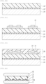
- Figs. 2A to 2E are views for explaining one aspect of producing a laminate.
- the semiconductor substrate 1 having the bumps 1a is prepared ( Fig. 2A ).
- the surface of the semiconductor substrate 1 on which the bump 1a is present is coated with the release agent composition to form the release agent layer 2 ( Fig. 2B ).
- the adhesive composition is applied onto the release agent layer 2 to form an adhesive coating layer 3a ( Fig. 2C ).
- the support substrate 4 is disposed on the adhesive coating layer 3a ( Fig. 2D ).
- a heating apparatus (not illustrated; a hot plate) is disposed on the surface opposite to the surface of the semiconductor substrate 1 on which the bump 1a is present, and the adhesive coating layer 3a is heated and cured by the heating apparatus to be converted into the adhesive layer 3 ( Fig. 2E ).
- a laminate is obtained by the steps shown in Figs. 2A to 2E .
- the above-described production method has been described as an example.
- the production can be performed by a method including Step 1 of forming an adhesive coating layer by coating the surface of the semiconductor substrate with the an adhesive composition and, if necessary, heating the adhesive composition, Step 2 of forming a release agent layer by coating the surface of the support substrate with a release agent composition and, if necessary, heating the release agent composition, and Step 3 of obtaining a laminate by applying a load in the thickness direction of the semiconductor substrate and the support substrate to bring the semiconductor substrate and the support substrate into close contact with each other while performing at least one of the heat treatment and the pressure reduction treatment, then performing a post-heat treatment.
- the laminate having the electronic device layer is used for processing the electronic device layer. While the electronic device layer is being processed, the electronic device layer is adhered to the support substrate. After processing the electronic device layer, the release agent layer is irradiated with light, and then the electronic device layer is separated from the support substrate.
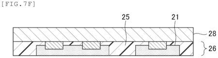
- the semiconductor chip substrate 21 fixed onto the adhesive layer 22 is sealed using the sealing resin 25.
- the plurality of semiconductor chip substrates 21 temporarily adhered onto the support substrate 24 via the adhesive layer 22 is sealed with the sealing resin 25.
- the electronic device layer 26, which includes the semiconductor chip substrate 21 and the sealing resin 25 disposed in the semiconductor chip substrate 21, is formed on the adhesive layer 22, and as described above, the electronic device layer 26 is a base material layer in which a plurality of semiconductor chip substrates are embedded in the sealing resin.
- a sealing resin heated to 130 to 170°C is supplied onto the adhesive layer 22 to cover the semiconductor chip substrate 21 while maintaining a high viscosity state, and is compression-molded to form a layer including the sealing resin 25 on the adhesive layer 22.
- the temperature condition is, for example, 130 to 170°C.
- the pressure applied to the semiconductor chip substrate 21 is, for example, 50 to 500 N/cm 2 .
- a method for producing a processed semiconductor substrate or a method for producing a processed electronic device layer can be provided.
- the method for producing a processed semiconductor substrate according to the present invention includes the following Step 5A and the following Step 6A.
- the method for producing the processed electronic device layer may further include the following Step 7A.
- Step 6A is a step of separating the processed semiconductor substrate and the support substrate in Step 5A.
- Step 7A is a step of cleaning the processed semiconductor substrate after Step 6A.
- examples of the method for separating (releasing) the semiconductor substrate and the support substrate include a method for mechanical releasing with equipment having a sharp part, a releasing method for separation between the support and the semiconductor wafer, and the like after the photoirradiation to the release agent layer, but are not limited thereto.
- the properties of the release agent layer are changed (for example, separation or decomposition of the release agent layer) as described above, and thereafter, for example, one of the substrates is pulled up, and the semiconductor substrate and the support substrate can be easily separated from each other.
- the release agent layer is not necessarily irradiated with light over the entire region of the release agent layer. Even when the region irradiated with light and the region not irradiated with light are mixed, the semiconductor substrate and the support substrate can be separated from each other by a slight external force such as pulling up of the support substrate as long as the release agent layer as a whole has sufficiently improved releasing ability.
- the ratio and positional relationship between the region irradiated with light and the region not irradiated with light vary depending on the type and specific composition of the adhesive to be used, the thickness of the adhesive layer, the thickness of the adhesive layer, the thickness of the release agent layer, the intensity of light to be irradiated, and the like, but those skilled in the art can appropriately set conditions without requiring an excessive test.
- the method for producing a processed semiconductor substrate of the present invention for example, in a case where the support substrate of the laminate to be used is light-transmissive, it is possible to shorten the photoirradiation time when releasing is performed by photoirradiation from the support substrate side, and as a result, not only improvement in throughput can be expected, but also physical stress and the like required for releasing can be avoided, and the semiconductor substrate and the support substrate can be easily and efficiently separated from each other only by photoirradiation.
- the irradiation amount of light for release is 50 to 3,000 mJ/cm 2 .
- the irradiation time is appropriately determined according to the wavelength and the irradiation amount.
- the wavelength of light used for release is preferably, for example, a wavelength of 250 to 600 nm, and more preferably a wavelength of 250 to 370 nm.
- a more suitable wavelength is 308 nm, 343 nm, 355 nm, 365 nm, or 532 nm.
- the irradiation amount of light required for release is an irradiation amount that can cause suitable change in properties, for example, decomposition of the Novolac resin.
- the light used for release may be laser light or non-laser light emitted from a light source such as an ultraviolet lamp.
- the substrate can be cleaned by spraying the cleaning agent composition onto the surface of at least one of the separated semiconductor substrate and the support substrate, or immersing the separated semiconductor substrate or the support substrate in the cleaning agent composition.
- the surface of the processed semiconductor substrate or the like may be cleaned using a removal tape or the like.
- Step 7A of cleaning the processed semiconductor substrate may be performed after Step 6A.
- cleaning agent composition to be used for cleaning examples include the following.
- the cleaning agent composition usually contains a salt and a solvent.
- a suitable example of the cleaning agent composition includes a cleaning agent composition containing a quaternary ammonium salt and a solvent.
- Such quaternary ammonium cations typically include tetra (hydrocarbon) ammonium cations.
- the solvent contained in the cleaning agent composition is not particularly limited as long as the solvent is used for this type of application and dissolves a salt such as a quaternary ammonium salt, but from the viewpoint of obtaining a cleaning agent composition having excellent cleanability with good reproducibility, the viewpoint of obtaining a cleaning agent composition having excellent uniformity by dissolving a salt such as a quaternary ammonium salt satisfactorily, and the like, the cleaning agent composition preferably contains one or more amide-based solvents.
- constituent elements and method elements related to the above-described steps of the method for producing a processed semiconductor substrate of the present invention may be variously changed without departing from the gist of the present invention.
- the method for producing a processed semiconductor substrate of the present invention may include steps other than the above-described steps.
- the semiconductor substrate or the support substrate of the laminate of the present invention when the semiconductor substrate or the support substrate of the laminate of the present invention is light-transmissive, the semiconductor substrate and the support substrate of the laminate are separated from each other by irradiating the release agent layer with light from the semiconductor substrate side or the support substrate side.
- the semiconductor substrate and the support substrate are temporarily adhered to each other by the adhesive layer and the release agent layer to be suitably releasable, for example, when the support substrate is light-transmissive, the semiconductor substrate and the support substrate can be easily separated from each other by irradiating the release agent layer with light from the support substrate side of the laminate.
- releasing is performed after the semiconductor substrate of the laminate is processed.
- a laminate is prepared ( Fig. 6A ). This laminate is the same laminate as the laminate shown in Figs. 1 and 2E .
- the thinned semiconductor substrate 1 and the support substrate 4 are released using a releasing apparatus (not illustrated). Then, the thinned semiconductor substrate 1 is obtained ( Fig. 6C ).
- residues of the release agent layer 2 and the adhesive layer 3 may remain on the thinned semiconductor substrate 1. Therefore, it is preferable to clean the thinned semiconductor substrate 1 using the cleaning agent composition to remove the residues of the release agent layer 2 and the adhesive layer 3 from the semiconductor substrate 1.
- Step 5B is a step of processing the electronic device layer in the laminate described in the section of
- Step 6B is a step of separating the electronic device layer processed in Step 5B from the support substrate.
- Examples of the processing performed on the electronic device layer in Step 5B include a grinding step and a wiring layer forming step.
- the wiring layer forming step is a step of forming a wiring layer on the exposed semiconductor chip substrate 21 after the grinding step.
- a wiring layer 28 is formed on the electronic device layer 26 including the semiconductor chip substrate 21 and a layer of the sealing resin 25.
- the wiring layer 28 is also called a redistribution layer (RDL), is a thin-film wiring body constituting wiring connected to a substrate, and may have a single-layer or multi-layer structure.
- the wiring layer may be one in which wiring is formed by a conductor (for example, metals such as aluminum, copper, titanium, nickel, gold, and silver, and alloys such as silver-tin alloys) between dielectrics (photosensitive resin such as silicon oxide (SiO x ) and photosensitive epoxy), but is not limited thereto.
- Examples of the method for forming the wiring layer 28 include the following methods.
- a dielectric layer of silicon oxide (SiO x ), a photosensitive resin, or the like is formed on the layer of the sealing resin 25.
- the dielectric layer made of silicon oxide can be formed by, for example, a sputtering method, a vacuum vapor deposition method, or the like.
- the dielectric layer made of a photosensitive resin can be formed by coating the layer of the sealing resin 25 with a photosensitive resin by a method such as spin coating, dipping, roller blade, spray coating, or slit coating.
- wiring is formed on the dielectric layer with a conductor such as metal.
- a known semiconductor process method such as lithography processing such as photolithography (registry lithography) or etching processing can be used.
- lithography processing include lithography processing using a positive resist material and lithography processing using a negative resist material.
- a bump can be further formed on the wiring layer 28 or an element can be mounted.
- the element can be mounted on the wiring layer 28 using, for example, a chip mounter or the like.
- the laminate according to the fourth embodiment may be a laminate produced in a process based on a fan-out type technology in which a terminal provided on a semiconductor chip substrate is mounted on a wiring layer extending outside a chip area.
- the properties of the release agent layer are changed (for example, separation or decomposition of the release agent layer) as described above, and thereafter, for example, one of the substrates is pulled up, and the electronic device layer and the support substrate can be easily separated from each other.
- PCzBA has the following repeating units.
- PCzNA target polymer
- PCzNA has the following repeating units.
- PCzFL a target polymer
- the weight average molecular weight Mw of PCzFL measured in terms of polystyrene by GPC was 2,600.
- the obtained polymer was dissolved in PGMEA, and ion exchange was performed using a cation exchange resin and an anion exchange resin for 4 hours to obtain a target polymer solution.
- PCzFL has the following repeating units.
- DPAEHA target polymer
- the weight average molecular weight Mw of DPAEHA measured in terms of polystyrene by GPC was 1,200.
- the obtained polymer was dissolved in PGMEA, and ion exchange was performed using a cation exchange resin and an anion exchange resin for 4 hours to obtain a target polymer solution.
- DPAEHA has the following repeating units.
- 86.36 g of 1,4-dioxane and 86.36 g of toluene were added to 56.02 g of 1-phenylnaphthylamine, 50.00 g of 1-pyrenecarboxaldehyde (manufactured by Maruzen Chemicals Co., Ltd.), 6.67 g of 4-(trifluoromethyl)benzaldehyde, and 2.46 g of methanesulfonic acid, and the mixture was stirred under reflux for 18 hours under a nitrogen atmosphere. After completion of the reaction, the mixture was diluted with 96 g of tetrahydrofuran, and the diluted solution was added dropwise to methanol to obtain a precipitate. The obtained precipitate was filtered, cleaned with methanol, and dried at 60°C for 24 hours to obtain a target polymer (hereinafter abbreviated as PPNAPCA-F).
- PPNAPCA-F target polymer
- the weight average molecular weight of PPNAPCA-F measured by GPC in terms of standard polystyrene was 1,100.
- the obtained polymer was dissolved in PGMEA, and ion exchange was performed using a cation exchange resin and an anion exchange resin for 4 hours to obtain a target polymer solution.
- PPNAPCA-F has the following structural units in the following proportions:
- a 100 mm silicon wafer (thickness: 770 ⁇ m) as a device-side wafer (semiconductor substrate) is coated with the releasable composition obtained in Preparation Examples 2-1 to 2-6 and Comparative Preparation Examples 2-1 to 2-6 by spin coating, and heated at 200°C for 5 minutes to form a release agent layer on the silicon wafer such that the final thickness of the release agent layer was approximately 1,500 nm.
- a semiconductor substrate and a 100 mm glass wafer (thickness: 500 ⁇ m) as a support substrate were bonded to sandwich the adhesive coating layer and the release agent layer, and heated on a hot plate at 200°C for 10 minutes with the semiconductor substrate side facing down (post-heat treatment) to prepare a laminate.
- bonding was performed at a temperature of 23°C and a degree of vacuum of 1,000 Pa.
Landscapes
- Chemical & Material Sciences (AREA)
- Organic Chemistry (AREA)
- Health & Medical Sciences (AREA)
- Chemical Kinetics & Catalysis (AREA)
- Medicinal Chemistry (AREA)
- Polymers & Plastics (AREA)
- Phenolic Resins Or Amino Resins (AREA)
- Compositions Of Macromolecular Compounds (AREA)
- Macromonomer-Based Addition Polymer (AREA)
- Paints Or Removers (AREA)
Applications Claiming Priority (2)
| Application Number | Priority Date | Filing Date | Title |
|---|---|---|---|
| JP2022135765 | 2022-08-29 | ||
| PCT/JP2023/030881 WO2024048493A1 (ja) | 2022-08-29 | 2023-08-28 | 光照射剥離用の剥離剤組成物、積層体、及び加工された半導体基板の製造方法 |
Publications (1)
| Publication Number | Publication Date |
|---|---|
| EP4583149A1 true EP4583149A1 (en) | 2025-07-09 |
Family
ID=90099892
Family Applications (1)
| Application Number | Title | Priority Date | Filing Date |
|---|---|---|---|
| EP23860255.1A Pending EP4583149A1 (en) | 2022-08-29 | 2023-08-28 | Release agent composition for photoirradiation release, laminate, and method for producing processed semiconductor substrate |
Country Status (7)
| Country | Link |
|---|---|
| US (1) | US20260011598A1 (https=) |
| EP (1) | EP4583149A1 (https=) |
| JP (1) | JPWO2024048493A1 (https=) |
| KR (1) | KR20250060227A (https=) |
| CN (1) | CN119631160A (https=) |
| TW (1) | TW202409750A (https=) |
| WO (1) | WO2024048493A1 (https=) |
Families Citing this family (1)
| Publication number | Priority date | Publication date | Assignee | Title |
|---|---|---|---|---|
| WO2025198034A1 (ja) * | 2024-03-22 | 2025-09-25 | 日産化学株式会社 | 加工された半導体基板の製造方法 |
Family Cites Families (8)
| Publication number | Priority date | Publication date | Assignee | Title |
|---|---|---|---|---|
| JP4565804B2 (ja) | 2002-06-03 | 2010-10-20 | スリーエム イノベイティブ プロパティズ カンパニー | 被研削基材を含む積層体、その製造方法並びに積層体を用いた極薄基材の製造方法及びそのための装置 |
| KR100471638B1 (ko) | 2003-01-09 | 2005-02-21 | 이성규 | 섬유 가공기용 진공탈수장치 |
| JP5580800B2 (ja) | 2010-10-29 | 2014-08-27 | 東京応化工業株式会社 | 積層体、およびその積層体の分離方法 |
| KR20120106486A (ko) | 2011-03-18 | 2012-09-26 | (주) 에스와이씨 | 절단면 표면 특성 개선을 위한 피처리물 절단 장치 |
| US11472168B2 (en) | 2017-11-01 | 2022-10-18 | Nissan Chemical Corporation | Laminated body including novolac resin as peeling layer |
| KR102036600B1 (ko) | 2018-01-02 | 2019-10-25 | 이이엘씨이이주식회사 | 3차원 입체물 제조 로봇 시스템을 위한 오븐 유닛 |
| EP4187575A4 (en) * | 2020-07-22 | 2024-08-28 | Nissan Chemical Corporation | Multilayer body, release agent composition, and method for producing processed semiconductor substrate |
| KR102895979B1 (ko) * | 2020-11-30 | 2025-12-04 | 닛산 가가쿠 가부시키가이샤 | 적층체, 적층체의 제조 방법, 및 반도체 기판의 제조 방법 |
-
2023
- 2023-08-28 JP JP2024544228A patent/JPWO2024048493A1/ja active Pending
- 2023-08-28 WO PCT/JP2023/030881 patent/WO2024048493A1/ja not_active Ceased
- 2023-08-28 CN CN202380057101.XA patent/CN119631160A/zh active Pending
- 2023-08-28 KR KR1020257009351A patent/KR20250060227A/ko active Pending
- 2023-08-28 TW TW112132285A patent/TW202409750A/zh unknown
- 2023-08-28 US US19/105,945 patent/US20260011598A1/en active Pending
- 2023-08-28 EP EP23860255.1A patent/EP4583149A1/en active Pending
Also Published As
| Publication number | Publication date |
|---|---|
| TW202409750A (zh) | 2024-03-01 |
| WO2024048493A1 (ja) | 2024-03-07 |
| US20260011598A1 (en) | 2026-01-08 |
| JPWO2024048493A1 (https=) | 2024-03-07 |
| KR20250060227A (ko) | 2025-05-07 |
| CN119631160A (zh) | 2025-03-14 |
Similar Documents
| Publication | Publication Date | Title |
|---|---|---|
| EP4398285A1 (en) | Adhesive composition, multilayer body, and method for producing processed semiconductor substrate | |
| EP4369380A1 (en) | Layered body manufacturing method, and kit for adhesive composition | |
| EP4583149A1 (en) | Release agent composition for photoirradiation release, laminate, and method for producing processed semiconductor substrate | |
| EP4678708A1 (en) | Adhesive composition, laminate, and method for producing processed semiconductor substrate | |
| EP4653507A1 (en) | Adhesive composition, laminate, and method for producing processed semiconductor substrate | |
| EP4653508A1 (en) | Adhesive composition, laminate, and method for producing processed semiconductor substrate | |
| EP4678709A1 (en) | Adhesive composition, laminate, and method for producing processed semiconductor substrate | |
| EP4636051A1 (en) | Releaser composition for photoirradiation release, and adhesive composition for photoirradiation release | |
| JP2024135070A (ja) | 剥離剤組成物、積層体、及び加工された半導体基板又は電子デバイス層の製造方法 | |
| WO2025094889A1 (ja) | 接着剤組成物、積層体、及び加工された半導体基板の製造方法 | |
| WO2025094880A1 (ja) | 接着剤組成物、積層体、及び加工された半導体基板の製造方法 | |
| WO2025057891A1 (ja) | 接着剤組成物、積層体、及び加工された半導体基板の製造方法 | |
| WO2025094864A1 (ja) | 接着剤組成物、積層体、及び加工された半導体基板の製造方法 | |
| TW202611252A (zh) | 接著劑組成物、積層體、及加工後之半導體基板之製造方法 | |
| WO2025094887A1 (ja) | 接着剤組成物、積層体、及び加工された半導体基板の製造方法 | |
| WO2026028984A1 (ja) | 接着剤組成物、積層体、及び加工された半導体基板の製造方法 |
Legal Events
| Date | Code | Title | Description |
|---|---|---|---|
| STAA | Information on the status of an ep patent application or granted ep patent |
Free format text: STATUS: THE INTERNATIONAL PUBLICATION HAS BEEN MADE |
|
| PUAI | Public reference made under article 153(3) epc to a published international application that has entered the european phase |
Free format text: ORIGINAL CODE: 0009012 |
|
| STAA | Information on the status of an ep patent application or granted ep patent |
Free format text: STATUS: REQUEST FOR EXAMINATION WAS MADE |
|
| 17P | Request for examination filed |
Effective date: 20250213 |
|
| AK | Designated contracting states |
Kind code of ref document: A1 Designated state(s): AL AT BE BG CH CY CZ DE DK EE ES FI FR GB GR HR HU IE IS IT LI LT LU LV MC ME MK MT NL NO PL PT RO RS SE SI SK SM TR |
|
| DAV | Request for validation of the european patent (deleted) | ||
| DAX | Request for extension of the european patent (deleted) |