EP4582958A2 - Betriebsarten für ein-/ausgabegerät für ein system mit speicherpools - Google Patents
Betriebsarten für ein-/ausgabegerät für ein system mit speicherpools Download PDFInfo
- Publication number
- EP4582958A2 EP4582958A2 EP25178075.5A EP25178075A EP4582958A2 EP 4582958 A2 EP4582958 A2 EP 4582958A2 EP 25178075 A EP25178075 A EP 25178075A EP 4582958 A2 EP4582958 A2 EP 4582958A2
- Authority
- EP
- European Patent Office
- Prior art keywords
- locations
- memory
- subset
- processing unit
- central processing
- Prior art date
- Legal status (The legal status is an assumption and is not a legal conclusion. Google has not performed a legal analysis and makes no representation as to the accuracy of the status listed.)
- Pending
Links
Images



Classifications
-
- G—PHYSICS
- G06—COMPUTING OR CALCULATING; COUNTING
- G06F—ELECTRIC DIGITAL DATA PROCESSING
- G06F13/00—Interconnection of, or transfer of information or other signals between, memories, input/output devices or central processing units
- G06F13/14—Handling requests for interconnection or transfer
- G06F13/20—Handling requests for interconnection or transfer for access to input/output bus
- G06F13/28—Handling requests for interconnection or transfer for access to input/output bus using burst mode transfer, e.g. direct memory access DMA, cycle steal
-
- G—PHYSICS
- G06—COMPUTING OR CALCULATING; COUNTING
- G06F—ELECTRIC DIGITAL DATA PROCESSING
- G06F12/00—Accessing, addressing or allocating within memory systems or architectures
- G06F12/02—Addressing or allocation; Relocation
- G06F12/08—Addressing or allocation; Relocation in hierarchically structured memory systems, e.g. virtual memory systems
- G06F12/0802—Addressing of a memory level in which the access to the desired data or data block requires associative addressing means, e.g. caches
- G06F12/0806—Multiuser, multiprocessor or multiprocessing cache systems
- G06F12/0842—Multiuser, multiprocessor or multiprocessing cache systems for multiprocessing or multitasking
-
- G—PHYSICS
- G06—COMPUTING OR CALCULATING; COUNTING
- G06F—ELECTRIC DIGITAL DATA PROCESSING
- G06F12/00—Accessing, addressing or allocating within memory systems or architectures
- G06F12/02—Addressing or allocation; Relocation
- G06F12/0223—User address space allocation, e.g. contiguous or non contiguous base addressing
- G06F12/0284—Multiple user address space allocation, e.g. using different base addresses
-
- G—PHYSICS
- G06—COMPUTING OR CALCULATING; COUNTING
- G06F—ELECTRIC DIGITAL DATA PROCESSING
- G06F12/00—Accessing, addressing or allocating within memory systems or architectures
- G06F12/02—Addressing or allocation; Relocation
- G06F12/08—Addressing or allocation; Relocation in hierarchically structured memory systems, e.g. virtual memory systems
- G06F12/0802—Addressing of a memory level in which the access to the desired data or data block requires associative addressing means, e.g. caches
- G06F12/0806—Multiuser, multiprocessor or multiprocessing cache systems
-
- G—PHYSICS
- G06—COMPUTING OR CALCULATING; COUNTING
- G06F—ELECTRIC DIGITAL DATA PROCESSING
- G06F12/00—Accessing, addressing or allocating within memory systems or architectures
- G06F12/02—Addressing or allocation; Relocation
- G06F12/08—Addressing or allocation; Relocation in hierarchically structured memory systems, e.g. virtual memory systems
- G06F12/0802—Addressing of a memory level in which the access to the desired data or data block requires associative addressing means, e.g. caches
- G06F12/0806—Multiuser, multiprocessor or multiprocessing cache systems
- G06F12/084—Multiuser, multiprocessor or multiprocessing cache systems with a shared cache
-
- G—PHYSICS
- G06—COMPUTING OR CALCULATING; COUNTING
- G06F—ELECTRIC DIGITAL DATA PROCESSING
- G06F12/00—Accessing, addressing or allocating within memory systems or architectures
- G06F12/02—Addressing or allocation; Relocation
- G06F12/08—Addressing or allocation; Relocation in hierarchically structured memory systems, e.g. virtual memory systems
- G06F12/0802—Addressing of a memory level in which the access to the desired data or data block requires associative addressing means, e.g. caches
- G06F12/0844—Multiple simultaneous or quasi-simultaneous cache accessing
- G06F12/0846—Cache with multiple tag or data arrays being simultaneously accessible
-
- G—PHYSICS
- G06—COMPUTING OR CALCULATING; COUNTING
- G06F—ELECTRIC DIGITAL DATA PROCESSING
- G06F12/00—Accessing, addressing or allocating within memory systems or architectures
- G06F12/02—Addressing or allocation; Relocation
- G06F12/08—Addressing or allocation; Relocation in hierarchically structured memory systems, e.g. virtual memory systems
- G06F12/10—Address translation
- G06F12/1081—Address translation for peripheral access to main memory, e.g. direct memory access [DMA]
-
- G—PHYSICS
- G06—COMPUTING OR CALCULATING; COUNTING
- G06F—ELECTRIC DIGITAL DATA PROCESSING
- G06F12/00—Accessing, addressing or allocating within memory systems or architectures
- G06F12/02—Addressing or allocation; Relocation
- G06F12/08—Addressing or allocation; Relocation in hierarchically structured memory systems, e.g. virtual memory systems
- G06F12/10—Address translation
- G06F12/109—Address translation for multiple virtual address spaces, e.g. segmentation
-
- G—PHYSICS
- G06—COMPUTING OR CALCULATING; COUNTING
- G06F—ELECTRIC DIGITAL DATA PROCESSING
- G06F13/00—Interconnection of, or transfer of information or other signals between, memories, input/output devices or central processing units
- G06F13/14—Handling requests for interconnection or transfer
- G06F13/16—Handling requests for interconnection or transfer for access to memory bus
- G06F13/1668—Details of memory controller
-
- G—PHYSICS
- G06—COMPUTING OR CALCULATING; COUNTING
- G06F—ELECTRIC DIGITAL DATA PROCESSING
- G06F12/00—Accessing, addressing or allocating within memory systems or architectures
- G06F12/02—Addressing or allocation; Relocation
- G06F12/06—Addressing a physical block of locations, e.g. base addressing, module addressing, memory dedication
- G06F12/0607—Interleaved addressing
-
- G—PHYSICS
- G06—COMPUTING OR CALCULATING; COUNTING
- G06F—ELECTRIC DIGITAL DATA PROCESSING
- G06F12/00—Accessing, addressing or allocating within memory systems or architectures
- G06F12/02—Addressing or allocation; Relocation
- G06F12/08—Addressing or allocation; Relocation in hierarchically structured memory systems, e.g. virtual memory systems
- G06F12/0802—Addressing of a memory level in which the access to the desired data or data block requires associative addressing means, e.g. caches
- G06F12/0806—Multiuser, multiprocessor or multiprocessing cache systems
- G06F12/0813—Multiuser, multiprocessor or multiprocessing cache systems with a network or matrix configuration
-
- G—PHYSICS
- G06—COMPUTING OR CALCULATING; COUNTING
- G06F—ELECTRIC DIGITAL DATA PROCESSING
- G06F2212/00—Indexing scheme relating to accessing, addressing or allocation within memory systems or architectures
- G06F2212/10—Providing a specific technical effect
- G06F2212/1016—Performance improvement
- G06F2212/1024—Latency reduction
-
- G—PHYSICS
- G06—COMPUTING OR CALCULATING; COUNTING
- G06F—ELECTRIC DIGITAL DATA PROCESSING
- G06F2212/00—Indexing scheme relating to accessing, addressing or allocation within memory systems or architectures
- G06F2212/60—Details of cache memory
- G06F2212/6042—Allocation of cache space to multiple users or processors
-
- G—PHYSICS
- G06—COMPUTING OR CALCULATING; COUNTING
- G06F—ELECTRIC DIGITAL DATA PROCESSING
- G06F2212/00—Indexing scheme relating to accessing, addressing or allocation within memory systems or architectures
- G06F2212/65—Details of virtual memory and virtual address translation
- G06F2212/657—Virtual address space management
-
- G—PHYSICS
- G06—COMPUTING OR CALCULATING; COUNTING
- G06F—ELECTRIC DIGITAL DATA PROCESSING
- G06F2213/00—Indexing scheme relating to interconnection of, or transfer of information or other signals between, memories, input/output devices or central processing units
- G06F2213/28—DMA
Definitions
- safety-critical applications In a time-partitioned safety-critical system, safety-critical applications have to be properly time-budgeted such that the application execution time is sufficient to accommodate the execution of the designated application functionality.
- the time-budgeting of safety-critical applications is based on its worst-case time budgets and it is often referred to as Worst-Case Execution Time (WCET).
- WCET Worst-Case Execution Time
- a computing system includes at least one central processing unit, one or more central processing unit caches, and a main memory comprising a plurality of locations. Each location of the plurality of locations maps to a set in the one or more central processing unit caches. A first subset of locations of the plurality of locations are partitioned for one or more threads of a first application and assigned to non-contiguous memory locations of the main memory based on a respective set of one or more sets in the one or more central processing unit caches to which each location is mapped.
- the computing system further includes a first input/output (I/O) device configured to store data in a second subset of locations of the plurality of locations that are different from the first subset of locations partitioned for the one or more threads of the first application.
- the second subset of locations are non-contiguous memory locations of the main memory that are separated in address space according to a predefined pattern.
- Modern computing platforms in the avionics domain are characterized by their timing non-determinism because there might be multiple sources of memory interference (e.g., processor cores, Direct Memory Accesses (DMAs), graphics processing unit (GPU), and specialized co-processors).
- the timing non-determinism makes the application WCET difficult to determine.
- the application WCET is often empirically measured by introducing cross-interference to the shared hardware resources.
- An example of a shared hardware resource can be for example the memory hierarchy - memory buses, caches, memory controllers, and DDR memory.
- One effective means to bound interference between applications and thus reduce its WCET is to partition/isolate by allocating a dedicated hardware shared resources to specific application(s).
- the memory allocated to each application is not contiguous. For example, one application may be allocated every 16th memory page, and the next application may be allocated the next page and every 16th memory page from that page. Each cache-unique set of pages is considered as a cache partition.
- Memory pools typically encompass one or more cache pools according to the cache and memory needs of the applications.
- the memory management unit (MMU) of the processor is configured to make any set of pages allocated to an application appear to be contiguous to the application, so the application sees a virtual address space that is contiguous even though the allocated underlying physical memory region is not contiguous.
- I/O devices for example, DMA engines, GPUs, or co-processors
- I/O devices save data in the main memory using physically contiguous memory regions, which are only compatible with a computing system utilizing memory pools if these regions are uncached from the processor's perspective. This is because accesses to such regions by an application would pollute many or all of the memory pools by evicting data when reading or by leaving dirty data behind in pools in which the application has no quota. This is because these contiguous regions, if more than a page in size, will cut across the cache partitions allocated to each application.
- these computing systems utilizing memory pools typically allocate shared I/O data to uncached memory regions even if the IO device is capable of snooping the CPU's cache. Accesses by CPU cores to uncached memory regions to read or write I/O data are much slower than to cached regions, so while necessary to protect the integrity of the cache partitioning, performance is impacted by this strategy.
- the example systems and methods described herein enable a computing system using memory pools to interact with I/O devices that respect an existing CPU cache partitioning strategy.
- cache effects associated with DMA operations can be constrained to a single memory pool, and CPU accesses to the I/O memory space can be performed using fast cached accesses rather than slow uncached accesses. This yields a reduction in WCET for the application accessing the I/O resource.
- cache effects are limited to one memory pool, applications utilizing other memory pools see no impact to their cache state, thus their WCET is unaffected.
- platform performance is improved when utilizing an I/O device (for example, an I/O device such as DMA, GPU, or co-processor).
- FIG. 1 illustrates a block diagram of an example computing system 100.
- the computing system 100 includes at least one central processing unit (CPU) 102, one or more CPU caches 104, a main memory 106, and one or more input/output (I/O) devices 108.
- CPU central processing unit
- CPU caches central processing unit
- main memory main memory
- I/O input/output
- the computing system includes multiple CPUs 102 that share memory resources (CPU cache 104 and main memory 106).
- the computing system 100 includes a microprocessor chip 101 that includes N CPUs, or cores, which are capable of executing one or more threads in parallel.
- Each CPU is coupled to at least a CPU cache 104 (for example, level 1 (L1) cache).
- the CPU cache 104 contains memory and computing logic, and the CPU cache 104 is coupled to main memory 106.
- the main memory 106 can also be coupled to secondary storage (not shown).
- the CPU cache 104 in the computing system is generally a smaller, faster memory than main memory 106.
- the configuration shown in FIG. 1 and other arrangements and processes described herein are set forth for purposes of example only, and other arrangements and elements (e.g., machines, interfaces, functions, orders of elements, etc.) can be added or used instead.
- other arrangements and elements e.g., machines, interfaces, functions, orders of elements, etc.
- many of the elements described herein are functional entities that may be implemented as discrete components or in conjunction with other components, in any suitable combination and location.
- the computing system 100 may consist of multiple independent CPU busses so that each CPU can access the CPU cache 104 and other components without contending for a CPU bus with the other CPUs.
- the computing system 100 may include more than one cache (for example, an L2 and/or L3 cache), which may be either within the microprocessor chip 101 or part of another chip in the computing system 100. Even further, a system may contain multiple independent main memories and secondary storages, not shown in FIG. 1 . Each unit of memory in the computing system 100 may comprise semiconductor memory, magnetic memory, optical memory, acoustic memory, biological memory, or any combination of these memory technologies, or any other memory technology used in conjunction with computational devices.
- cache for example, an L2 and/or L3 cache
- Each unit of memory in the computing system 100 may comprise semiconductor memory, magnetic memory, optical memory, acoustic memory, biological memory, or any combination of these memory technologies, or any other memory technology used in conjunction with computational devices.
- the purpose of the CPU cache 104 in the computing system 100 is to temporarily hold instructions, data, or both, that are being used by tasks executing on one of CPUs 102.
- patterns of computer memory access exhibit both spatial and temporal locality of reference. That is, once a main memory 106 location is accessed, it is likely that a nearby main memory location will also be accessed, and it is also likely that main memory 106 location will again be accessed soon.
- a fast-memory cache such as CPU cache 104, because it is likely that a CPU 102 will once again have to access one of those main memory locations.
- CPU cache 104 is typically much smaller than main memory 106 means that not all main memory locations can be simultaneously resident in CPU cache 104. In order to maintain performance, CPU cache 104 typically will execute a simple operation to map a main memory location to a limited number of CPU cache locations (cache associativity). In some examples, the computing system 100 is configured to avoid cache related interference between applications being executed by the CPUs 102 using similar techniques to those described in the '308 patent. For example, the computing system 100 is configured to store one or more threads of respective applications in main memory locations that map to respective portions of the CPU cache 104.
- the one or more I/O device 108 are communicatively coupled to the main memory 106 and configured to read/write data to/from the main memory 106.
- at least one I/O device 108 is also communicatively coupled to the CPU 102 and/or the CPU cache 104.
- the one or more I/O devices 108 can be a DMA engine, a GPU, co-processor, or a hardware accelerator utilized by the computing system 100.
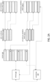
- FIGS. 2A-2C illustrate diagrams of example patterns of non-contiguous memory locations of the main memory 106 for different I/O scenarios. It should be understood that some connections between components are omitted from FIG. 2C for ease of illustration, and that the features included in FIGS. 2A-2B could also be included in FIG. 2C .
- an I/O device 108 is configured to directly write/read data to/from the physical memory.
- the I/O device 108 is directly communicatively coupled to the main memory locations 204-2, 224-2, and the I/O device 108 is configured to directly write/read I/O data to/from the main memory locations 204-2, 224-2 via the link between the I/O device 108 and the main memory locations 204-2, 224-2.
- the most recent memory requests are cached prior to be written to the main memory 106.
- the I/O device 108 is communicatively coupled to the cache 104, and the I/O device 108 is configured to cache the I/O data via the link between the I/O device 108 and the cache 104.
- the I/O data is included in the cache 104 and only then the cached I/O data is written to the main memory 106.
- the CPUs 102 are configured to perform uncached memory transfers in certain situations.
- the CPUs 102 are communicatively coupled to the virtual address space 202-2, 222-2, and the CPUs 102 are optionally configured to write/read data with uncached memory transfers via the link between the CPUs 102 and the virtual address space 202-2, 222-2.
- the CPUs 102 are communicatively coupled to the I/O device 108.
- the link from the CPUs 102 to the I/O device 108 is used for control and particularly where the CPUs 102 are the master and the I/O device 108 is the slave in the computing systems shown.
- the line from the I/O device 108 to the CPUs 102 is optionally included and can be used for signaling (for example, through interrupts) the CPUs 102 when data transfer is completed by the I/O device.
- the I/O device 108 is configured to have its own memory pool(s) that is distinct from the memory pools for an application (Application A in FIG. 2A ) executed by the CPUs 102.
- the I/O device 108 is configured to store I/O data in a subset of locations 204-2 of the main memory 106 that map to different memory pools of the CPU cache 104 than those that are allocated to one or more threads of the application.
- At least one of the I/O devices 108 is configured to be a private I/O device 108 for a specific application (Application A in FIG. 2B ) executed by the CPU(s) 102 and share the cache partition and memory pool with the specific application.
- the I/O device 108 is configured to store I/O data in a subset of locations of the main memory 106 that map to the portions of the CPU cache 104 partitioned for the specific application.
- the subset of locations 224-2 where the I/O device 108 stores the I/O data are non-contiguous memory locations 224-2 of the main memory 106 and the locations are separated in address space according to a predefined pattern that is the same as the pattern used for storing the one or more threads of the specific application in non-contiguous memory locations 224-1.
- the non-contiguous memory locations allocated for the I/O data from the I/O device 108 will be included in the CPU cache partition for the specific application.
- two or more of the I/O devices 108-1, 108-2 are configured to be private I/O devices 108 for a specific application (Application A in FIG. 2C ) executed by the CPU(s) 102 and share the cache partition and memory pool with the specific application.
- the I/O devices 108-1, 108-2 are configured to store I/O data in respective subsets of locations of the main memory that map to the portions of the CPU cache 104 partitioned for the specific application.
- the subset of locations 244-2 where the I/O device 108-1 stores the I/O data are non-contiguous memory locations 244-2 of the main memory 106 and the locations are separated in address space according to a predefined pattern that is the same as the pattern used for storing the one or more threads of the specific application in non-contiguous memory locations 244-1.
- the subset of locations where the I/O device 108-2 stores the I/O data are non-contiguous memory locations 244-3 of the main memory 106 and the locations are separated in address space according to a predefined pattern that is the same as the pattern used for storing the one or more threads of the specific application in non-contiguous memory locations 244-1.
- the non-contiguous memory locations allocated for the I/O data from the I/O devices 108-1, 108-2 will be aligned to the memory pool for the specific application.
- At least one of the I/O devices 108 is configured to be shared by two or more applications executed by the CPU(s) 102.
- the I/O device 108 is configured to store I/O data in a subset of locations of the main memory that map to the portions of the CPU cache 104 partitioned for each respective application.
- a first subset of locations where the I/O device 108 stores the I/O data are non-contiguous memory locations of the main memory 106 and the locations are separated in address space according to a predefined pattern that is the same as the pattern used for storing the one or more threads of a first application in non-contiguous memory locations
- a second subset of locations where the I/O device 108 stores the I/O data are non-contiguous memory locations of the main memory 106 and the locations are separated in address space according to a predefined pattern that is the same as the pattern used for storing the one or more threads of a second application non-contiguous memory locations.
- the first and second subsets of non-contiguous memory locations allocated for the I/O data from the I/O device 108 will be included in the cache partition for the first and second applications, respectively.
- the one or more I/O devices 108 can be configured to operate in different operational modes that enable I/O data to be read from and write to the non-contiguous memory locations of the main memory 106.
- the one or more I/O devices 108 are configured to operate in a linked-list descriptor mode.
- a linked-list descriptor mode includes reading/writing data to different addresses using pointers that indicate where data is to be read/written next. Rather than starting at a particular address and reading/writing data to contiguous memory locations in a sequential manner, a linked-list descriptor mode enables the I/O device 108 to store I/O data in non-contiguous memory locations of the main memory 106 as defined in the linked-list.
- the computing system 100 is configured to utilize software-only to enable the one or more I/O devices 108 to respect the memory pools of the one or more applications executed by the CPU(s) 102.
- the CPUs 102 are configured to call an I/O device 108 to perform a data transfer.
- the predefined non-contiguous memory access pattern utilized by the I/O device 108 can be stored in the main memory 106.
- the predefined non-contiguous memory access pattern is represented as a linked-list
- the one or more I/O devices 108 are configured to retrieve the linked-list descriptors from the main memory 106 prior to each time the I/O devices 108 input data to the main memory 106 in order to determine where to store the I/O data.
- the descriptor tables in the main memory are precomputed for particular page masks, but the source and destination addresses need to be taken into account or computed.
- the computing system 100 utilizes specialized hardware and software to enable the I/O devices 108 to respect the memory pools of the one or more applications executed by the CPU(s) 102. Similar to the software-only configuration, the CPUs 102 can be configured to command an I/O device 108 to perform a data transfer. However, in some specialized hardware and software examples, the one or more I/O devices 108 are configured to interact with a memory management unit (MMU) of the computing system 100 in order to access the page table used for the computing system 100 rather than retrieving the non-contiguous memory access pattern (for example, linked-list descriptors) from the main memory 106.
- MMU memory management unit
- the I/O device 108 is configured to perform a continuous read/write and the MMU is configured to save the I/O data to the particular non-contiguous locations of the main memory 106.
- the computing system 100 includes an I/O MMU configured to provide I/O address translation for I/O data to/from the I/O device 108.
- the I/O device 108 is configured to interact with the microprocessor chip 101 directly via a specialized interface. In some such examples, the I/O device 108 is configured to determine the predefined pattern either from an I/O configuration interface or directly from the processor architecture. In some such examples, the I/O device 108 includes a set of registers that includes the page mask, the source and destination addresses, and bytes to be read/written. In such examples, the I/O device 108 is configured to determine the predefined pattern (for example, using logic, state machines, etc.) based on the information in the set of registers (for example, using the page mask and destination address).
- the I/O device 108 or other component of the computing system 100 is configured to automatically copy the I/O data that is saved in the non-contiguous memory locations of the main memory 106 to the CPU cache 104.
- the CPU(s) 102 would be enabled to access the I/O data more quickly than if the CPU(s) had to read the data from the main memory 106 into the CPU cache 104.
- FIG. 3 illustrates a flow diagram of an example method 300 for data input/output for a computing system utilizing memory pools.
- the common features discussed above with respect to computing system 100 with respect to FIGS. 1-2C can include similar characteristics to those discussed with respect to method 300 and vice versa.
- the method 300 is performed using one or more components of the computing system 100.
- the method 300 includes dividing the CPU cache into a plurality of memory pools (block 302).
- the CPU cache is divided such that each application executed by the CPUs of a computing system has a respective memory pool assigned to it.
- the method 300 further includes dividing the main memory into a plurality of locations that map to the memory pools (block 304) and assigning one or more threads of a first application to a first subset of the plurality of main memory locations associated with a first memory pool (block 306).
- the first subset of the plurality of main memory locations is a non-contiguous set of locations of the main memory that are separated in address space according to a predefined pattern.
- the method 300 further includes assigning I/O data from a first I/O device to a second subset of the plurality of main memory locations associated with the first memory pool or a second memory pool (block 308).
- the I/O device can be, for example, a DMA engine, GPU, co-processor, or hardware accelerator.
- the second subset of the plurality of main memory locations is a non-contiguous set of locations of the main memory that are separated in address space according to a predefined pattern.
- the first I/O device is exclusively used by the first application.
- the I/O data from the first I/O device is saved in the main memory using a similar pattern to the one or more threads of the first application (for example, as discussed above with respect to FIG. 2B ) and associated with the first memory pool.
- the first I/O device is not exclusively used (or used at all) by the first application.
- the I/O data from the first I/O device is saved in the main memory using a wholly different pattern than the pattern used to save the one or more threads of the first application.
- the first I/O device is shared by multiple applications.
- the I/O data from the first I/O device is saved in the main memory in a similar pattern to that used for saving each of the one or more threads of the multiple applications. For example, a subset of the I/O data saved by the first I/O device is saved in the main memory using a similar pattern used to save the one or more threads of the first application and another subset of the I/O data saved by the first I/O device is saved in the main memory using a similar pattern used to save the one or more threads of the second application.
- the method optionally includes assigning I/O data from other I/O device(s) to other subset(s) of the plurality of main memory locations associated with the first memory pool or a second memory pool (block 310).
- the other I/O device can be the same type as the first I/O device or could also be different.
- the other subset(s) of the plurality of main memory locations are non-contiguous set of locations of the main memory that are separated in address space according to a predefined pattern, which may be the same or different as the patterns used to associate data with the first memory pool or the second memory pool.
- the systems and methods described herein provide enable the computing system 100 to use CPU cache partitions and memory pools and also access I/O data as a cached transaction, which is typically many times faster than uncached transactions of the previous systems.
- the CPUs are more efficient with cached transactions and the WCET when utilizing an I/O device (for example, a DMA, GPU, or co-processor) is greatly reduced.
- I/O device for example, a DMA, GPU, or co-processor
- the systems and methods described herein can be utilized in high-performance system to efficiently handle high-throughput network interfaces using multiple DMA engines to send/receive data to a GPU or other co-processor.
- the systems and methods described herein can also be used to accelerate machine learning applications and aid other I/O intensive applications.
- system elements, method steps, or examples described throughout this disclosure may be implemented on one or more computer systems, field programmable gate array (FPGA), application specific integrated circuit (ASIC) or similar devices comprising hardware executing code to realize those elements, processes, or examples, said code stored on a non-transient data storage device.
- FPGA field programmable gate array
- ASIC application specific integrated circuit
- These devices include or function with software programs, firmware, or other computer readable instructions for carrying out various methods, process tasks, calculations, and control functions, used in a distributed antenna system.
- the computer readable medium can be implemented as any available media that can be accessed by a general purpose or special purpose computer or processor, or any programmable logic device.
- Suitable processor-readable media may include storage or memory media such as magnetic or optical media.
- storage or memory media may include conventional hard disks, Compact Disk - Read Only Memory (CD-ROM), volatile or non-volatile media such as Random Access Memory (RAM) (including, but not limited to, Synchronous Dynamic Random Access Memory (SDRAM), Double Data Rate (DDR) RAM, RAMBUS Dynamic RAM (RDRAM), Static RAM (SRAM), etc.), Read Only Memory (ROM), Electrically Erasable Programmable ROM (EEPROM), and flash memory, etc.
- RAM Random Access Memory
- SDRAM Synchronous Dynamic Random Access Memory
- DDR Double Data Rate
- RDRAM RAMBUS Dynamic RAM
- SRAM Static RAM
- ROM Read Only Memory
- EEPROM Electrically Erasable Programmable ROM
- flash memory etc.
- Suitable processor-readable media may also include transmission media such as electrical, electromagnetic, or digital signals, conveyed via a communication medium such as a network and/or a wireless link.
- the methods and techniques described here may be implemented in digital electronic circuitry, or with a programmable processor (for example, a special-purpose processor or a general-purpose processor such as a computer) firmware, software, or in combinations of them.
- Apparatus embodying these techniques may include appropriate input and output devices, a programmable processor, and a storage medium tangibly embodying program instructions for execution by the programmable processor.
- a process embodying these techniques may be performed by a programmable processor executing a program of instructions to perform desired functions by operating on input data and generating appropriate output.
- the techniques may advantageously be implemented in one or more programs that are executable on a programmable system including at least one programmable processor coupled to receive data and instructions from, and to transmit data and instructions to, a data storage system, at least one input device, and at least one output device.
- a processor will receive instructions and data from a read-only memory and/or a random access memory.
- Storage devices suitable for tangibly embodying computer program instructions and data include all forms of non-volatile memory, including by way of example semiconductor memory devices, such as EPROM, EEPROM, and flash memory devices; magnetic disks such as internal hard disks and removable disks; magneto-optical disks; and DVD disks. Any of the foregoing may be supplemented by, or incorporated in, specially-designed application-specific integrated circuits (ASICs).
- ASICs application-specific integrated circuits
- Example 1 includes a computing system, comprising: at least one central processing unit; one or more central processing unit caches; a main memory comprising a plurality of locations, wherein each location of the plurality of locations maps to a set in the one or more central processing unit caches, wherein a first subset of locations of the plurality of locations are partitioned for one or more threads of a first application and assigned to non-contiguous memory locations of the main memory based on a respective set of one or more sets in the one or more central processing unit caches to which each location is mapped; and a first input/output (I/O) device configured to store data in a second subset of locations of the plurality of locations that are different from the first subset of locations partitioned for the one or more threads of the first application, wherein the second subset of locations are non-contiguous memory locations of the main memory that are separated in address space according to a predefined pattern.
- I/O input/output
- Example 2 includes the computing system of Example 1, wherein the first I/O device is a direct memory access (DMA) engine, a graphics processing unit (GPU), or a co-processor, wherein the first I/O device is configured to input data to the main memory and/or output data from the main memory.
- DMA direct memory access
- GPU graphics processing unit
- co-processor wherein the first I/O device is configured to input data to the main memory and/or output data from the main memory.
- Example 3 includes the computing system of any of Examples 1-2, wherein the second subset of locations are mapped to different sets of the one or more central processing unit caches than the first subset of locations.
- Example 4 includes the computing system of any of Examples 1-2, wherein the second subset of locations are mapped to the same sets of the one or more central processing unit caches as the first subset of locations.
- Example 5 includes the computing system of any of Examples 1-4, further comprising a second I/O device configured to store data in a third subset of locations of the plurality of locations that are distinct from the first subset of locations partitioned for the one or more threads of the first application and the second subset of locations, wherein the third subset of locations are non-contiguous memory locations of the main memory that are separated in address space according to the predefined pattern used for the first subset of non-contiguous memory locations and mapped to the same sets of the one or more central processing unit caches for the first subset of locations.
- a second I/O device configured to store data in a third subset of locations of the plurality of locations that are distinct from the first subset of locations partitioned for the one or more threads of the first application and the second subset of locations, wherein the third subset of locations are non-contiguous memory locations of the main memory that are separated in address space according to the predefined pattern used for the first subset of non-contiguous memory locations and mapped to the
- Example 6 includes the computing system of any of Examples 1-5, further comprising a second I/O device configured to store data in a third subset of locations of the plurality of locations that are distinct from the first subset of locations partitioned for the one or more threads of the first application and the second subset of locations, wherein the third subset of locations are non-contiguous memory locations of the main memory that are separated according to a second predefined pattern and mapped to different sets of the one or more central processing unit caches than the first subset of locations and the second subset of locations.
- a second I/O device configured to store data in a third subset of locations of the plurality of locations that are distinct from the first subset of locations partitioned for the one or more threads of the first application and the second subset of locations, wherein the third subset of locations are non-contiguous memory locations of the main memory that are separated according to a second predefined pattern and mapped to different sets of the one or more central processing unit caches than the first subset of locations and the second subset of
- Example 7 includes the computing system of Example 6, further comprising a third I/O device configured to store data in a fourth subset of locations of the plurality of locations that are distinct from the first subset of locations partitioned for the one or more threads of the first application, the second subset of locations, and the third subset of locations, wherein the fourth subset of locations are non-contiguous memory locations of the main memory that are separated according to a third predefined pattern and mapped to different sets of the one or more central processing unit caches than the first subset of locations, the second subset of locations, and the third subset of locations.
- a third I/O device configured to store data in a fourth subset of locations of the plurality of locations that are distinct from the first subset of locations partitioned for the one or more threads of the first application, the second subset of locations, and the third subset of locations, wherein the fourth subset of locations are non-contiguous memory locations of the main memory that are separated according to a third predefined pattern and mapped to different sets of the one
- Example 8 includes the computing system of any of Examples 1-7, wherein the predefined pattern is stored in the main memory and represented as a linked-list, wherein the first I/O device is configured to retrieve the linked-list when inputting data to the main memory.
- Example 9 includes the computing system of any of Examples 1-8, further comprising a memory management unit, wherein the I/O device is configured to determine the predefined pattern either from an I/O configuration interface or directly from a processor architecture.
- Example 10 includes a computing system, comprising: at least one central processing unit; one or more central processing unit caches; a main memory comprising a plurality of locations, wherein each location of the plurality of locations maps to a set in the one or more central processing unit caches, wherein a first subset of locations of the plurality of locations are partitioned for one or more threads of a first application and assigned to non-contiguous memory locations of the main memory based on a respective set of one or more sets in the one or more central processing unit caches to which each location is mapped, wherein a second subset of locations of the plurality of locations are partitioned for one or more threads of a second application and assigned to non-contiguous memory locations of the main memory based on a respective set of one or more sets in the one or more central processing unit caches to which each location is mapped; and a first input/output (I/O) device configured to store data in a third subset of locations of the plurality of locations and a fourth subset of locations
- Example 11 includes the computing system of Example 10, wherein the first I/O device is a direct memory access (DMA) engine, a graphics processing unit (GPU), or a co-processor, wherein the first I/O device is configured to input data to the main memory and/or output data from the main memory.
- DMA direct memory access
- GPU graphics processing unit
- co-processor wherein the first I/O device is configured to input data to the main memory and/or output data from the main memory.
- Example 12 includes the computing system of any of Examples 10-11, further comprising a second I/O device configured to store data in a fifth subset of locations of the plurality of locations that are distinct from the first subset of locations partitioned for the one or more threads of the first application, the second subset of locations partitioned for the one or more threads of the second application, the third subset of locations and the fourth subset of locations, wherein the fifth subset of locations are non-contiguous memory locations of the main memory that are separated in address space according to the first predefined pattern used for the first subset of non-contiguous memory locations and mapped to the same sets of the one or more central processing unit caches for the first subset of locations.
- a second I/O device configured to store data in a fifth subset of locations of the plurality of locations that are distinct from the first subset of locations partitioned for the one or more threads of the first application, the second subset of locations partitioned for the one or more threads of the second application, the third subset of locations and the
- Example 13 includes the computing system of any of Examples 10-12, further comprising a second I/O device configured to store data in a fifth subset of locations of the plurality of locations that are distinct from the first subset of locations partitioned for the one or more threads of the first application, the second subset of locations partitioned for the one or more threads of the second application, the third subset of locations and the fourth subset of locations, wherein the fifth subset of locations are non-contiguous memory locations of the main memory that are separated according to a third predefined pattern and mapped to different sets of the one or more central processing unit caches than the first subset of locations and the second subset of locations.
- a second I/O device configured to store data in a fifth subset of locations of the plurality of locations that are distinct from the first subset of locations partitioned for the one or more threads of the first application, the second subset of locations partitioned for the one or more threads of the second application, the third subset of locations and the fourth subset of locations, wherein the fifth
Landscapes
- Engineering & Computer Science (AREA)
- Theoretical Computer Science (AREA)
- Physics & Mathematics (AREA)
- General Engineering & Computer Science (AREA)
- General Physics & Mathematics (AREA)
- Memory System Of A Hierarchy Structure (AREA)
- Information Transfer Systems (AREA)
- Debugging And Monitoring (AREA)
Applications Claiming Priority (2)
| Application Number | Priority Date | Filing Date | Title |
|---|---|---|---|
| US17/087,221 US11847074B2 (en) | 2020-11-02 | 2020-11-02 | Input/output device operational modes for a system with memory pools |
| EP21205391.2A EP3992802B1 (de) | 2020-11-02 | 2021-10-28 | Betriebsarten für eingabe-/ausgabevorrichtungen für ein system mit speicherpools |
Related Parent Applications (2)
| Application Number | Title | Priority Date | Filing Date |
|---|---|---|---|
| EP21205391.2A Division-Into EP3992802B1 (de) | 2020-11-02 | 2021-10-28 | Betriebsarten für eingabe-/ausgabevorrichtungen für ein system mit speicherpools |
| EP21205391.2A Division EP3992802B1 (de) | 2020-11-02 | 2021-10-28 | Betriebsarten für eingabe-/ausgabevorrichtungen für ein system mit speicherpools |
Publications (2)
| Publication Number | Publication Date |
|---|---|
| EP4582958A2 true EP4582958A2 (de) | 2025-07-09 |
| EP4582958A3 EP4582958A3 (de) | 2025-07-30 |
Family
ID=78414427
Family Applications (2)
| Application Number | Title | Priority Date | Filing Date |
|---|---|---|---|
| EP21205391.2A Active EP3992802B1 (de) | 2020-11-02 | 2021-10-28 | Betriebsarten für eingabe-/ausgabevorrichtungen für ein system mit speicherpools |
| EP25178075.5A Pending EP4582958A3 (de) | 2020-11-02 | 2021-10-28 | Betriebsarten für ein-/ausgabegerät für ein system mit speicherpools |
Family Applications Before (1)
| Application Number | Title | Priority Date | Filing Date |
|---|---|---|---|
| EP21205391.2A Active EP3992802B1 (de) | 2020-11-02 | 2021-10-28 | Betriebsarten für eingabe-/ausgabevorrichtungen für ein system mit speicherpools |
Country Status (2)
| Country | Link |
|---|---|
| US (2) | US11847074B2 (de) |
| EP (2) | EP3992802B1 (de) |
Families Citing this family (3)
| Publication number | Priority date | Publication date | Assignee | Title |
|---|---|---|---|---|
| US11847074B2 (en) | 2020-11-02 | 2023-12-19 | Honeywell International Inc. | Input/output device operational modes for a system with memory pools |
| US12204952B2 (en) | 2022-03-24 | 2025-01-21 | Honeywell International S.R.O. | Systems and method for thermal management of computing systems |
| US12493570B2 (en) * | 2023-09-26 | 2025-12-09 | Microchip Technology Incorporated | Device and methods for functional descriptor-based DMA controller |
Citations (1)
| Publication number | Priority date | Publication date | Assignee | Title |
|---|---|---|---|---|
| US8069308B2 (en) | 2008-02-13 | 2011-11-29 | Honeywell International Inc. | Cache pooling for computing systems |
Family Cites Families (22)
| Publication number | Priority date | Publication date | Assignee | Title |
|---|---|---|---|---|
| US6370622B1 (en) | 1998-11-20 | 2002-04-09 | Massachusetts Institute Of Technology | Method and apparatus for curious and column caching |
| US6732255B1 (en) | 1999-09-15 | 2004-05-04 | Koninklijke Philips Electronics N.V. | Can microcontroller that permits concurrent access to different segments of a common memory by both the processor core and the DMA engine thereof |
| US6938252B2 (en) * | 2000-12-14 | 2005-08-30 | International Business Machines Corporation | Hardware-assisted method for scheduling threads using data cache locality |
| US7039768B2 (en) * | 2003-04-25 | 2006-05-02 | International Business Machines Corporation | Cache predictor for simultaneous multi-threaded processor system supporting multiple transactions |
| US8266379B2 (en) * | 2003-06-02 | 2012-09-11 | Infineon Technologies Ag | Multithreaded processor with multiple caches |
| US8868790B2 (en) | 2004-02-13 | 2014-10-21 | Oracle International Corporation | Processor-memory module performance acceleration in fabric-backplane enterprise servers |
| US7424553B1 (en) | 2004-04-15 | 2008-09-09 | Xilinx, Inc. | Method and apparatus for communicating data between a network transceiver and memory circuitry |
| US7984241B2 (en) * | 2005-09-16 | 2011-07-19 | Hewlett-Packard Development Company, L.P. | Controlling processor access to cache memory |
| WO2008057833A2 (en) | 2006-11-08 | 2008-05-15 | Sicortex, Inc. | System and method for remote direct memory access without page locking by the operating system |
| US7895392B2 (en) * | 2007-01-05 | 2011-02-22 | International Business Machines | Color-based cache monitoring |
| US9189282B2 (en) * | 2009-04-21 | 2015-11-17 | Empire Technology Development Llc | Thread-to-core mapping based on thread deadline, thread demand, and hardware characteristics data collected by a performance counter |
| US20110055482A1 (en) * | 2009-08-28 | 2011-03-03 | Broadcom Corporation | Shared cache reservation |
| AU2011213795A1 (en) * | 2011-08-19 | 2013-03-07 | Canon Kabushiki Kaisha | Efficient cache reuse through application determined scheduling |
| US9684600B2 (en) * | 2011-11-30 | 2017-06-20 | International Business Machines Corporation | Dynamic process/object scoped memory affinity adjuster |
| US9390010B2 (en) | 2012-12-14 | 2016-07-12 | Intel Corporation | Cache management |
| WO2015069408A1 (en) | 2013-11-05 | 2015-05-14 | Oracle International Corporation | System and method for supporting efficient packet processing model and optimized buffer utilization for packet processing in a network environment |
| US20150205724A1 (en) * | 2014-01-20 | 2015-07-23 | Honeywell International Inc. | System and method of cache partitioning for processors with limited cached memory pools |
| US9824015B2 (en) | 2015-05-29 | 2017-11-21 | Qualcomm Incorporated | Providing memory management unit (MMU) partitioned translation caches, and related apparatuses, methods, and computer-readable media |
| US9812221B1 (en) | 2015-09-09 | 2017-11-07 | Rockwell Collins, Inc. | Multi-core cache coherency built-in test |
| US10515017B2 (en) | 2017-02-23 | 2019-12-24 | Honeywell International Inc. | Memory partitioning for a computing system with memory pools |
| US10366007B2 (en) | 2017-12-11 | 2019-07-30 | Honeywell International Inc. | Apparatuses and methods for determining efficient memory partitioning |
| US11847074B2 (en) | 2020-11-02 | 2023-12-19 | Honeywell International Inc. | Input/output device operational modes for a system with memory pools |
-
2020
- 2020-11-02 US US17/087,221 patent/US11847074B2/en active Active
-
2021
- 2021-10-28 EP EP21205391.2A patent/EP3992802B1/de active Active
- 2021-10-28 EP EP25178075.5A patent/EP4582958A3/de active Pending
-
2023
- 2023-11-20 US US18/514,872 patent/US12360930B2/en active Active
Patent Citations (1)
| Publication number | Priority date | Publication date | Assignee | Title |
|---|---|---|---|---|
| US8069308B2 (en) | 2008-02-13 | 2011-11-29 | Honeywell International Inc. | Cache pooling for computing systems |
Also Published As
| Publication number | Publication date |
|---|---|
| EP3992802B1 (de) | 2025-08-06 |
| US11847074B2 (en) | 2023-12-19 |
| EP4582958A3 (de) | 2025-07-30 |
| US20220138131A1 (en) | 2022-05-05 |
| US12360930B2 (en) | 2025-07-15 |
| US20240086349A1 (en) | 2024-03-14 |
| EP3992802A1 (de) | 2022-05-04 |
Similar Documents
| Publication | Publication Date | Title |
|---|---|---|
| US12360930B2 (en) | Input/output device operational modes for a system with memory pools | |
| JP6928123B2 (ja) | メモリシステム内のページマイグレーションのオーバヘッドを低減するメカニズム | |
| EP2476051B1 (de) | Systeme und verfahren zur verarbeitung von speicheranfragen | |
| US10545672B2 (en) | Method for accessing extended memory, device, and system | |
| US8180981B2 (en) | Cache coherent support for flash in a memory hierarchy | |
| US8451281B2 (en) | Shared virtual memory between a host and discrete graphics device in a computing system | |
| US20150106545A1 (en) | Computer Processor Employing Cache Memory Storing Backless Cache Lines | |
| US9678872B2 (en) | Memory paging for processors using physical addresses | |
| US10761986B2 (en) | Redirecting data to improve page locality in a scalable data fabric | |
| EP0408058A2 (de) | Mikroprozessor | |
| KR20170098187A (ko) | 저장 서브시스템을 위한 연관적 및 원자적 라이트-백 캐싱 시스템 및 방법 | |
| US11354244B2 (en) | Memory management device containing memory copy device with direct memory access (DMA) port | |
| US20170091092A1 (en) | Coherent interconnect for managing snoop operation and data processing apparatus including the same | |
| US20190018790A1 (en) | Method and apparatus for two-layer copy-on-write | |
| US10754791B2 (en) | Software translation prefetch instructions | |
| US20180107619A1 (en) | Method for shared distributed memory management in multi-core solid state drive | |
| US5293622A (en) | Computer system with input/output cache | |
| WO2008031678A1 (en) | Dmac address translation miss handling mechanism | |
| US20100257319A1 (en) | Cache system, method of controlling cache system, and information processing apparatus | |
| US5696938A (en) | Computer system permitting mulitple write buffer read-arounds and method therefor | |
| US7181587B1 (en) | Mapping an arbitrary number of contiguous memory pages at an arbitrary alignment | |
| EP0377969B1 (de) | Rechneranordnungen mit Ein-/Ausgabecachespeicher | |
| US20130262790A1 (en) | Method, computer program and device for managing memory access in a multiprocessor architecture of numa type | |
| CN117971716A (zh) | 缓存管理方法、设备、装置和存储介质 | |
| Dixon | Page associative caches on Futurebus |
Legal Events
| Date | Code | Title | Description |
|---|---|---|---|
| PUAI | Public reference made under article 153(3) epc to a published international application that has entered the european phase |
Free format text: ORIGINAL CODE: 0009012 |
|
| STAA | Information on the status of an ep patent application or granted ep patent |
Free format text: STATUS: THE APPLICATION HAS BEEN PUBLISHED |
|
| REG | Reference to a national code |
Ref country code: DE Ref legal event code: R079 Free format text: PREVIOUS MAIN CLASS: G06F0012081300 Ipc: G06F0012084200 |
|
| PUAL | Search report despatched |
Free format text: ORIGINAL CODE: 0009013 |
|
| AC | Divisional application: reference to earlier application |
Ref document number: 3992802 Country of ref document: EP Kind code of ref document: P |
|
| AK | Designated contracting states |
Kind code of ref document: A2 Designated state(s): AL AT BE BG CH CY CZ DE DK EE ES FI FR GB GR HR HU IE IS IT LI LT LU LV MC MK MT NL NO PL PT RO RS SE SI SK SM TR |
|
| AK | Designated contracting states |
Kind code of ref document: A3 Designated state(s): AL AT BE BG CH CY CZ DE DK EE ES FI FR GB GR HR HU IE IS IT LI LT LU LV MC MK MT NL NO PL PT RO RS SE SI SK SM TR |
|
| RIC1 | Information provided on ipc code assigned before grant |
Ipc: G06F 12/0842 20160101AFI20250624BHEP Ipc: G06F 12/0846 20160101ALI20250624BHEP Ipc: G06F 12/084 20160101ALI20250624BHEP Ipc: G06F 12/109 20160101ALI20250624BHEP Ipc: G06F 12/1081 20160101ALI20250624BHEP Ipc: G06F 13/28 20060101ALI20250624BHEP Ipc: G06F 12/02 20060101ALI20250624BHEP Ipc: G06F 12/06 20060101ALN20250624BHEP Ipc: G06F 12/0813 20160101ALN20250624BHEP |
|
| STAA | Information on the status of an ep patent application or granted ep patent |
Free format text: STATUS: REQUEST FOR EXAMINATION WAS MADE |
|
| 17P | Request for examination filed |
Effective date: 20250821 |
|
| GRAP | Despatch of communication of intention to grant a patent |
Free format text: ORIGINAL CODE: EPIDOSNIGR1 |
|
| STAA | Information on the status of an ep patent application or granted ep patent |
Free format text: STATUS: GRANT OF PATENT IS INTENDED |
|
| RIC1 | Information provided on ipc code assigned before grant |
Ipc: G06F 12/0842 20160101AFI20260211BHEP Ipc: G06F 12/0846 20160101ALI20260211BHEP Ipc: G06F 12/084 20160101ALI20260211BHEP Ipc: G06F 12/109 20160101ALI20260211BHEP Ipc: G06F 12/1081 20160101ALI20260211BHEP Ipc: G06F 13/28 20060101ALI20260211BHEP Ipc: G06F 12/02 20060101ALI20260211BHEP Ipc: G06F 12/06 20060101ALN20260211BHEP Ipc: G06F 12/0813 20160101ALN20260211BHEP |
|
| INTG | Intention to grant announced |
Effective date: 20260219 |