EP4580347A1 - Circuit for detection and mitigation of device damage to an electronic device - Google Patents
Circuit for detection and mitigation of device damage to an electronic device Download PDFInfo
- Publication number
- EP4580347A1 EP4580347A1 EP24220777.7A EP24220777A EP4580347A1 EP 4580347 A1 EP4580347 A1 EP 4580347A1 EP 24220777 A EP24220777 A EP 24220777A EP 4580347 A1 EP4580347 A1 EP 4580347A1
- Authority
- EP
- European Patent Office
- Prior art keywords
- transistor
- terminal
- value
- electronic device
- output
- Prior art date
- Legal status (The legal status is an assumption and is not a legal conclusion. Google has not performed a legal analysis and makes no representation as to the accuracy of the status listed.)
- Pending
Links
Images



Classifications
-
- H—ELECTRICITY
- H10—SEMICONDUCTOR DEVICES; ELECTRIC SOLID-STATE DEVICES NOT OTHERWISE PROVIDED FOR
- H10D—INORGANIC ELECTRIC SEMICONDUCTOR DEVICES
- H10D89/00—Aspects of integrated devices not covered by groups H10D84/00 - H10D88/00
- H10D89/60—Integrated devices comprising arrangements for electrical or thermal protection, e.g. protection circuits against electrostatic discharge [ESD]
- H10D89/601—Integrated devices comprising arrangements for electrical or thermal protection, e.g. protection circuits against electrostatic discharge [ESD] for devices having insulated gate electrodes, e.g. for IGFETs or IGBTs
- H10D89/811—Integrated devices comprising arrangements for electrical or thermal protection, e.g. protection circuits against electrostatic discharge [ESD] for devices having insulated gate electrodes, e.g. for IGFETs or IGBTs using FETs as protective elements
-
- H—ELECTRICITY
- H02—GENERATION; CONVERSION OR DISTRIBUTION OF ELECTRIC POWER
- H02H—EMERGENCY PROTECTIVE CIRCUIT ARRANGEMENTS
- H02H1/00—Details of emergency protective circuit arrangements
- H02H1/0007—Details of emergency protective circuit arrangements concerning the detecting means
-
- G—PHYSICS
- G01—MEASURING; TESTING
- G01R—MEASURING ELECTRIC VARIABLES; MEASURING MAGNETIC VARIABLES
- G01R31/00—Arrangements for testing electric properties; Arrangements for locating electric faults; Arrangements for electrical testing characterised by what is being tested not provided for elsewhere
- G01R31/28—Testing of electronic circuits, e.g. by signal tracer
- G01R31/317—Testing of digital circuits
- G01R31/31703—Comparison aspects, e.g. signature analysis, comparators
-
- H—ELECTRICITY
- H02—GENERATION; CONVERSION OR DISTRIBUTION OF ELECTRIC POWER
- H02H—EMERGENCY PROTECTIVE CIRCUIT ARRANGEMENTS
- H02H9/00—Emergency protective circuit arrangements for limiting excess current or voltage without disconnection
- H02H9/04—Emergency protective circuit arrangements for limiting excess current or voltage without disconnection responsive to excess voltage
- H02H9/041—Emergency protective circuit arrangements for limiting excess current or voltage without disconnection responsive to excess voltage using a short-circuiting device
-
- H—ELECTRICITY
- H03—ELECTRONIC CIRCUITRY
- H03K—PULSE TECHNIQUE
- H03K17/00—Electronic switching or gating, i.e. not by contact-making and –breaking
- H03K17/08—Modifications for protecting switching circuit against overcurrent or overvoltage
- H03K17/081—Modifications for protecting switching circuit against overcurrent or overvoltage without feedback from the output circuit to the control circuit
- H03K17/08104—Modifications for protecting switching circuit against overcurrent or overvoltage without feedback from the output circuit to the control circuit in field-effect transistor switches
-
- H—ELECTRICITY
- H10—SEMICONDUCTOR DEVICES; ELECTRIC SOLID-STATE DEVICES NOT OTHERWISE PROVIDED FOR
- H10D—INORGANIC ELECTRIC SEMICONDUCTOR DEVICES
- H10D89/00—Aspects of integrated devices not covered by groups H10D84/00 - H10D88/00
- H10D89/60—Integrated devices comprising arrangements for electrical or thermal protection, e.g. protection circuits against electrostatic discharge [ESD]
- H10D89/601—Integrated devices comprising arrangements for electrical or thermal protection, e.g. protection circuits against electrostatic discharge [ESD] for devices having insulated gate electrodes, e.g. for IGFETs or IGBTs
- H10D89/611—Integrated devices comprising arrangements for electrical or thermal protection, e.g. protection circuits against electrostatic discharge [ESD] for devices having insulated gate electrodes, e.g. for IGFETs or IGBTs using diodes as protective elements
Definitions
- This disclosure relates generally to circuit structures and methods for detecting and mitigating damage that may occur to an electronic device during device fabrication and, specifically, damage that may occur due to electrical discharge resulting from plasma-induced charges in a device's electrical structures.
- Semiconductor devices can be fabricated on insulative substrates. During device fabrication, such substrates sometimes accumulate charge in the substrate itself and in the devices formed or being formed on or in the substrate. If sufficient charge is accumulated, the charge is suddenly dissipated, potentially resulting in damage to the devices being fabricated on the substrate.
- SOC devices are often fabricated by forming a large number of isolated well structures (e.g., positive-well or PWELL structures) within the substrate. Those isolated well structures are often formed within larger well structures that are formed using opposite doping chemistry. Various SOC components can be formed within the isolated well structures, which provide improved isolation to reduce substrate noise coupling in the case of analog circuits.
- isolated well structures e.g., positive-well or PWELL structures
- PWELL structures positive-well or PWELL structures
- SOC components can be formed within the isolated well structures, which provide improved isolation to reduce substrate noise coupling in the case of analog circuits.
- the isolated well structures are connected to power or ground metal distributed networks.
- these power and ground distribution networks operate as metal antennas that collect the charges during plasma processing steps (e.g., during plasma etching).
- a discharge path from the driver located in one isolated WELL to a receiver located in another isolated WELL is established.
- WELL charging that occurs during plasma processing may cause a voltage difference across the gate oxide of the receiver, which can lead to gate oxide failure if the accumulated charge resulting into voltage difference exceeding the gate oxide breakdown voltage. Even if this does not cause device failure during fabrication, however, this weakens the gate oxide which may fail later in the field.
- Semiconductor devices find application in a wide variety of electronic components and systems.
- devices such as system-on-chip (SOC) devices
- device components are formed within isolated WELLs within the device substrate.
- SOC system-on-chip
- such devices may include drivers or receiver devices configured to process wireless (e.g., radio frequency) signal transmissions. These devices are often connected to antenna structures that are also formed over the device substrate to facilitate the transmission and reception of such wireless signals.
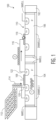
- FIG. 1 is a cross-sectional view of an SOC device 100.
- Device 100 includes a substrate 102 including isolated WELLs 104, 106.
- isolated WELL 104 includes a driver circuit that includes a transistor 108.
- Isolated WELL 106 includes a receiver circuit that includes transistor 110.
- an input terminal 120 of transistor 108 of isolated WELLs 104 is connected to antenna 112.
- An output terminal 122 of transistor 108 is connected, via electrical connection 116, to a gate terminal 118 of transistor 110 of isolated WELLs 106.
- electrical charge can accumulate within antenna 112. That charge also accumulates (as depicted by arrow 114) at a first terminal (e.g., a source or drain terminal) of transistor 108. When the charge has accumulated to a sufficient degree, the charge is discharged through connection 116 into the gate terminal 118 of transistor 110.
- the electrical discharge into gate terminal 118 can cause damage to transistor 110 and, specifically, the gate oxide material making up gate terminal 118 of transistor 110. This damage may cause transistor 110 to fail entirely (such that transistor 110 is never operational) or may cause sufficient damage the transistor 110 fails at a later date after fabrication of SOC device 100 is complete and the device has been operational in the field.
- the present disclosure proposes a circuit implementation configured to prevent, detect and correct the plasma-induced damage of SOC device gate oxide due to antenna-induced isolated WELL charging and device failure in the field due to aging.
- the present circuit approach is configured to detect plasma-induced damage (PID) via a self-test algorithm (see, for example, the method of FIG. 11 , described below). If a failure is detected (indicating some damage to device gate oxides), the present circuit may be utilized to remove the damaged device from the SOC device circuit to provide ongoing operations of the SOC, even if at reduced clock speeds.
- PID plasma-induced damage
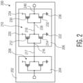
- FIG. 2 is a simplified depiction of a conventional SOC device 200 configured to implement a buffer circuit.
- Conventional SOC device 200 includes a substrate 202 including isolated WELL 204 and isolated WELL 206.
- Device 208 is formed within isolated WELL 204.
- Device 208 includes an electronic circuit (e.g., a transistor in combination with an antenna or antenna-like structure) that is susceptible to charge build-up during a plasma-based manufacturing process of conventional SOC device 200.
- a buffer 210 is formed within isolated WELL 206.
- Buffer 210 includes a transistor pair including transistor 212 and 214 connected between a power supply terminal and a ground terminal. Transistors 212 and 214 are connected in an inverter configuration with an input terminal 216 and an output terminal 218.
- Input terminal 216 is connected to device 208 via electrical connection 217 and to the gate terminals of transistors 212 and 214.
- the gate terminal of transistor 212 is inverting, so that transistor 212 is conductive when the value at input terminal 216 is a low value.
- the gate terminal of transistor 214 is non-inverting so that transistor 214 so that transistor 214 is conductive when the value at input terminal 216 is high.
- the value at output terminal 218 is equal to a high value (i.e., the level of power terminal 220) when the value at input terminal 216 is a low value.
- the value at output terminal is equal to a low value (i.e., the level of ground terminal 222) when the value at input terminal 216 is a high value.
- transistors 212 and 214 work in combination to invert the value at input terminal 216.
- transistors 230 and 232 are similarly configured in an inverter configuration between power terminal 234 and ground terminal 236.
- the inverter formed by transistors 230 and 232 has an input terminal 238 that is electrically connected to output terminal 218 of the inverter formed by transistors 212 and 214 and an output terminal 240.
- the two inverters formed by the first pair of transistors 212 and 214 and the second pair of transistors 230 and 232 forms a buffer in which the input value to buffer 210 received at input terminal 216 is replicated at output terminal 240.
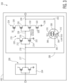
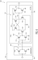
- FIG. 3 depicts a modified buffer circuit configuration in which additional circuit components are incorporated to protect the buffer circuit from damage due to electrical discharge occurring during device fabrication.
- FIG. 3 depicts the conventional SOC device 200 of FIG. 2 modified by the incorporation of additional circuit elements to form a new SOC device 300 provide electrical discharge protection.
- components in SOC device 300 are the same as those depicted in FIG. 2 (i.e., configured in the same manner and providing the same functionality), component element numbers are unchanged and the pertinent description of such components above is applicable.
- SOC device 300 includes a pair of transistors 320, 322 that have been added at the output stage of buffer 210.
- transistor 320 is connected between power terminal 234 and transistors 230.
- the control terminal of transistor 320 receives an input signal SE.
- Transistor 322 is connected between ground terminal 236 and transistors 232.
- the control terminal of transistor 322 receive an input signal SEB, which is the opposite of SE.
- buffer 210 is disabled and transistor 304 is enabled cause the input signal received at input terminal 216 to be supplied at output terminal 240.
- buffer 210 By supplying a particular input and toggling the control signal SE it is possible to selectively enable and disable the operation of buffer 210 and, correspondingly, transistor 304. Because the output of buffer 210 should match its input and because pass transistor 304 is configured to simply supply the input signal at input terminal 216 to output terminal 240, when toggling the value of SE, the output at output terminal 240 should not change if buffer 210 is operating correctly (i.e., has not been damaged).
- pass transistor 304 provide significant protection against electrical discharge, but by toggling the value of control signal SE and monitoring the output of buffer 210 it is possible to detect that buffer 210 is not operating correctly (e.g., as a buffer), which can be indicate of damage, which may be due to electrical discharge, for example, into the gate terminal of one or more of transistors 212, 214.
- control signal, SE may be set to a high value, in which buffer 210 is disabled and instead, pass transistor 304 operates as a buffer. Although this may enable ongoing error-free operations of SOC device 300, as mentioned above the configuration of pass transistor 304 may not enable operation of SOC device 300 at full clock-speeds. Accordingly, when bypassing buffer 210 the operational frequency of SOC device 300 may be reduced.
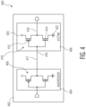
- FIG. 4 is a simplified depiction of a conventional SOC device 400 configured to implement an inverter.
- SOC device 400 includes a substrate 402 including isolated WELL 404 and isolated WELL 406.
- Device 408 is formed within isolated WELL 404.
- Device 408 includes an electronic circuit (e.g., a transistor in combination with an antenna or antenna-like structure) that is susceptible to charge build-up during a plasma-based manufacturing process of SOC device 400.
- Inverter 410 is formed within isolated WELL 406.
- Inverter 410 includes a transistor pair including transistor 412 and 414 connected between a power supply terminal 420 and ground terminal 422.
- Transistors 412 and 414 are connected in an inverter configuration with an input terminal 416 and an output terminal 418.
- Input terminal 416 is connected to device 408 via electrical connection 417 and to the gate terminals of transistors 412 and 414.
- the gate terminal of transistor 412 is inverting, so that transistor 412 is conductive when the value at input terminal 416 is a low value.
- the gate terminal of transistor 414 is non-inverting so that transistor 414 is conductive when the value at input terminal 416 is high. Accordingly, the value at output terminal 418 is equal to a high value (i.e., the level of power terminal 420) when the value at input terminal 416 is a low value.
- the value at output terminal is equal to a low value (i.e., the level of ground terminal 422) when the value at input terminal 416 is a high value.
- transistors 412 and 414 work in combination to invert the value at input terminal 416.
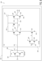
- FIG. 5 depicts a modified inverter circuit configuration in which additional circuit components are incorporated to protect the inverter circuit from damage due to electrical discharge occurring during device fabrication.
- FIG. 5 depicts the SOC device 400 of FIG. 4 modified by the incorporation of additional circuit elements to form SOC device 500 configured to provide electrical discharge protection.
- SOC device 500 is the same as those depicted in FIG. 4 (i.e., configured in the same manner and providing the same functionality)
- component element numbers are unchanged and the pertinent description of such components above is applicable.
- SOC device 500 includes a bypass path 502 that is connected between input terminal 416 of inverter 410 and output terminal 418.
- Bypass path 502 includes pass transistor 504.
- An input terminal of transistor 504 is connected to input terminal 416.
- Bypass path 502 includes inverter 506.
- An input terminal of inverter 506 is connected to an output terminal of transistor 504.
- Bypass path 502 includes pass transistor 508.
- An input terminal of pass transistor 508 is connected to an output terminal of inverter 506.
- An output terminal of pass transistor 508 is connected to output terminal 418.
- the control terminals of pass transistors 504 and 508 receive a selection input signal SE, which determine whether pass transistors 504 and 508 are conductive.
- Pass transistor 504 is formed within isolated WELL 406 and has a clamp diode configuration in which a pair of parasitic diodes are connected between a ground terminal and the input and output terminals of pass transistor 504.
- the parasitic clamp diodes are helpful to limit the positive charge buildup at its cathode, as an accumulation of this charge could result in an excessive voltage at this location. Should this voltage surpass the breakdown threshold of the parasitic clamp diode, it causes the diode to essentially create a direct path to ground. This action safeguards transistor 414 by preventing excess voltage from damaging it.
- Pass transistor 508 is formed within isolated WELL 406 and has a clamp diode configuration in which a pair of diodes are connected between a ground terminal and the input and output terminals of pass transistor 508.
- pass transistor 504 operates to protect transistors 412 and 414 from electrical discharge from isolated WELL 404 and into input terminal 416 that may occur during fabrication steps involving plasma operations. This results because if the electrical discharge reaches a significant value (e.g., one that may cause damage to any of transistors 412 and 414), the clamp diode configuration of pass transistors 504 can cause that electrical discharge to be passed to ground.
- SOC device 500 includes a pair of transistors 520, 522 that have been incorporated into inverter 410.
- Transistor 520 is connected between power terminal 420 and transistor 412.
- the control terminal of transistor 520 receives an input signal SE.
- Transistor 522 is connected between ground terminal 422 and transistor 414.
- the control terminal of transistor 522 receive an input signal SEB, which is the opposite of SE.
- inverter 410 is disabled - transistor 520 is turned off (due to the inversion at the control terminal of transistor 520) and, similarly, transistor 522 is turned off (due to the inverted control signal SEB being supplied at the control terminal).
- SE set to a high value
- inverter 410 is disabled and transistors 504 and 508 are enabled.
- the signal received at input terminal 416 passes through pass transistor 504, is inverted by inverter 506, passes through pass transistor 508 and is output at output terminal 418.
- bypass path 502 includes inverter 506, bypass path 502 operates as an inverter to mimic the functionality of inverter 410.
- isolation cell 810 includes a second input terminal 824 configured to receive a second signal EN that determines whether the isolation cell 810 is enabled. That input signal is inverted by the inverter made up of transistors 826 and 828 to generate an output signal B. If B has a high level, isolation cell 810 is enabled, and if B has a low value, isolation cell 810 is disabled.
- the control signal B is supplied to the gate control terminal of transistor 830, which is connected between transistor 814 and ground terminal 822.
- the same supply signal B is supplied at the gate or control terminal of transistor 832, which is connected between power supply terminal 820 and output terminal 818.
- Transistor 926 is connected between power supply terminal 820 and the control terminal of transistor 906.
- the control signal SE is supplied to the control terminal of transistor 926, which is an inverting terminal.
- transistor 926 when SE is high, transistor 926 is non-conductive, enabling operation of bypass path 902.
- SE when SE is low (e.g., during normal operations of SOC device 900 in which bypass path 902 is non-operative), transistor 926 is conductive, which connects the control terminal of transistor 906 to power supply terminal 820, which, due to the transistor's inverting control terminal makes transistor 906 non-conductive, effectively disabling bypass path 902.
- transistor 928 is connected between the control terminal of transistor 906 and ground node 930.
- the control signal SEB is supplied to the control terminal of transistor 928.
- SEB when SEB is low, transistor 928 is non-conductive, enabling operation of bypass path 902.
- SEB when SEB is high (e.g., during normal operations of SOC device 900 in which bypass path 902 is non-operative), transistor 928 is conductive, which connects the control terminal of transistor 908 to ground node 930, which makes transistor 908 non-conductive, effectively disabling bypass path 902.
- Transistor 932 is connected between a first terminal of transistor 812 and power supply terminal 820.
- the control terminal of transistor 932 receives the SE control input signal.
- the control terminal of transistor 932 is an inverting terminal such that when SE is high, transistor 932 is non-conductive, which disables the operation of inverter 842. Conversely, when SE is low, transistor 932 is conductive enabling normal operations of inverter 842.
- Transistor 934 is connected between transistor 814 and transistor 830.
- the control terminal of transistor 934 receives the SEB control input signal.
- SE SEB control input signal
- transistor 934 When SE is low, transistor 934 is non-conductive, which disables the operation of inverter 842. Conversely, when SEB is high, transistor 934 is conductive enabling normal operations of inverter 842.
- inverter 904 of bypass path 902 is disabled and isolation cell 810 can operate normally.
- inverter 842 is effectively disabled, and bypass path 902 is enabled such that inverter 904 supplies the inverted version of input signal A to input terminal 834 of inverter 844.
- inverter 842 it is possible to test the operation of inverter 842 to detect potential damage that may have resulted during plasma processing, as discussed above.
- by supplying particular input signals A and EN and toggling the control signal SE it is possible to selectively enable and disable the operation of inverter 842 and, correspondingly, transistors 812 and 814.
- the output at output terminal 846 should not change if inverter 842 is operating correctly (i.e., has not been damaged).
- inverter 842 is not operating correctly (e.g., as an inverter), which can be an indication of damage, which may be due to electrical discharge, for example, into the gate terminal of one or more of transistors 812 and 814.
- control signal SE may be set to a high value, in which case inverter 842 is disabled and instead, bypass path 902 operates as an inverter to enable ongoing error-free operations of SOC device 900.
- FIG. 10 is a block diagram depicting functional components of a device 1000 configured in accordance with the present disclosure.
- Device 1000 includes an electronic device 1002 (e.g., a buffer, inverter, level shifter, or isolation cell) that includes an input terminal 1004 and an output terminal 1006.
- Device 1000 includes a bypass path 1008 (e.g., bypass path 302, bypass path 502, bypass path 702, second bypass path 752, bypass path 902) that is connected between input terminal 1004 and output terminal 1006.
- Bypass path 1008 includes switch 1010 (e.g., pass transistor 304, pass transistors 504, pass transistor 704, pass transistor 754) that is controlled by a control signal received at control input 1012 of switch 1010.
- switch 1010 When the control signal has a first value, switch 1010 is open, which disables bypass path 1008 enabling normal operation of electronic device 1002. However, when the control signal has a second value, switch 1010 is closed, enabling bypass path 1008 and effectively bypassing electronic device 1002.
- Device 1000 includes switch 1014 (e.g., transistor 320 and transistor 322, transistor 520 and transistor 522, transistor 760 and transistor 762, bypass path 902) that is controlled by a control signal received at control input 1016 of switch 1014.
- the control signal received by control input 1016 of switch 1014 is inverted by inverter 1018 so that when the control signal has the first value, switch 1010 is closed, which enables the output of electronic device 1002 to be passed to output terminal 1006.
- control input 1016 is open, disconnecting electronic device 1002 from output terminal 1006 effectively disabling electronic device 1002.
- the control signal is received at control signal input 1020 as an output from demultiplexer 1022.
- Demultiplexer 1022 has a first input 1024 configured to receive an input based on the device configuration.
- a second input 1026 of demultiplexer 1022 is configured to receive an output from demultiplexer 1030.
- Demultiplexer 1022 receives a control input at control terminal 1028.
- the value of the control signal can be determined by the Fuse Bit or NVM bit.
- the value of the control signal can be determined by the output signal of demultiplexer 1030.
- Demultiplexer 1030 includes a first input 1032 configured to receive an input from a device test data register.
- Demultiplexer 1030 includes a second input 1034 configured to receive an input from a device pin 1036 or other electrical terminal accessible to external devices. The output of second input 1034 is determined by a control signal received at control input 1037, which selects whether the output of second input 1034 is the value stored in the test data register or the value at the device pin 1036.
- device 1000 may be placed in a normal mode of operation (e.g., where the output of control signal input 1020 is the first value of the control signal). In that case, bypass path 1008 is disabled.
- control signal can be set to the second value (e.g., via one or more input of the Fuse bit, the test data register, or the external control pin) enabling bypass path 1008 to be enabled and, at the same time, electronic device 1002 to be disabled.
- demultiplexer 1022 and demultiplexer 1030 provide various mechanisms by which bypass path 1008 can be selectively enabled to allow for test patterns to be executed on electronic device 1002 to detect potential malfunctions, such as those resulting from plasma induced discharge.
- method 1100 ends at block 1118 with an indication that there are no PID issues.
- the device may operate normally, however, as discussed above, because the device is operating nominally only due to the use of the various bypass paths or circuits described herein (as enabled by the high SE control signal input), the device may be configured to operate at a reduced operational frequency. This outcome is indicative of detection of a potential PID issue with the device.
- the method ends at block 1120 with an indication that the device has a potential non-PID related issue that requires diagnosis.
- the techniques described herein relate to a device, including: a substrate that includes a first isolated well and a second isolated well; a first electronic device formed within the first isolated well, the first electronic device including a first electronic circuit electrically connected to an antenna; and a second electronic device formed within the second isolated well, the second electronic device including: an input terminal that is electrically connected to the first electronic device, a second electronic circuit, the second electronic circuit including a first transistor, wherein a control terminal of the first transistor is electrically connected to the input terminal, a third electronic circuit including a clamp diode transistor, wherein the clamp diode is electrically connected to the input terminal, wherein the clamp diode transistor is configured to limit a voltage that may be applied to the control terminal of the first transistor and wherein the clamp diode transistor is configured to receive a control input signal, wherein when the control input signal has a first value the clamp diode transistor is conductive, and an output terminal electrically connected to the second electronic circuit and the third electronic circuit.
- the techniques described herein relate to a system, including: a device, including: a substrate that includes an isolated well, an electronic device within the isolated well, the electronic device including: an input terminal, a first electronic circuit including a first transistor, wherein a control terminal of the first transistor is electrically connected to the input terminal, a second electronic circuit including a clamp diode transistor, wherein the clamp diode is electrically connected to the input terminal, wherein the clamp diode transistor is configured to receive a control input signal and when the control input signal has a first value the clamp diode transistor is conductive, and an output terminal electrically connected to the first electronic circuit and the second electronic circuit; and a testing device configured to perform steps of: supplying a first input signal to the input terminal, switching the control input signal between the first value and a second value, and monitoring an output of the electronic device at the output terminal to detect a malfunction in the electronic device.
- the first electronic circuit is configured to receive the control input signal and wherein, when the control input signal has the first value, the first electronic circuit is disabled.
- the testing device to detect the malfunction in the second electronic device, is configured to perform steps of: when the control input signal has the first value, detect a first output value of an output signal of the electronic device at the output terminal; when the control input signal has the second value, detect a second output value of an output signal of the electronic device at the output terminal; and determine that the first output value is not equal to the second output value.
- the testing device to detect the malfunction in the second electronic device, is configured to perform steps of: setting the control input signal to the first value; determining a first result of a set of ATPG test patterns run on the second electronic device; setting the control input signal to the second value; determining a second result of the set of ATPG test patterns run on the second electronic device; and detecting the malfunction based on at least one of the first result and the second result.
- the testing device after detecting the malfunction, is configured to generate an output indicative of a plasma induced damage to the second electronic device.
- the terms “substantial” and “substantially” mean sufficient to accomplish the stated purpose in a practical manner and that minor imperfections, if any, are not significant for the stated purpose. Also as used herein, the terms “approximately” and “about” mean a value close to or within an acceptable range of an indicated value, amount, or quality, which also includes the exact indicated value itself.
Landscapes
- Engineering & Computer Science (AREA)
- General Engineering & Computer Science (AREA)
- Physics & Mathematics (AREA)
- General Physics & Mathematics (AREA)
- Semiconductor Integrated Circuits (AREA)
- Metal-Oxide And Bipolar Metal-Oxide Semiconductor Integrated Circuits (AREA)
Abstract
Description
- This disclosure relates generally to circuit structures and methods for detecting and mitigating damage that may occur to an electronic device during device fabrication and, specifically, damage that may occur due to electrical discharge resulting from plasma-induced charges in a device's electrical structures.
- Semiconductor devices can be fabricated on insulative substrates. During device fabrication, such substrates sometimes accumulate charge in the substrate itself and in the devices formed or being formed on or in the substrate. If sufficient charge is accumulated, the charge is suddenly dissipated, potentially resulting in damage to the devices being fabricated on the substrate.
- System-on-chip (SOC) devices are often fabricated by forming a large number of isolated well structures (e.g., positive-well or PWELL structures) within the substrate. Those isolated well structures are often formed within larger well structures that are formed using opposite doping chemistry. Various SOC components can be formed within the isolated well structures, which provide improved isolation to reduce substrate noise coupling in the case of analog circuits.
- In an SOC device, the isolated well structures are connected to power or ground metal distributed networks. During device fabrication, these power and ground distribution networks operate as metal antennas that collect the charges during plasma processing steps (e.g., during plasma etching). In SOC devices in which there are driver/receiver pairs placed in different isolated wells structures, but that are electrically connected to one another, a discharge path from the driver located in one isolated WELL to a receiver located in another isolated WELL is established. In such a configuration, WELL charging that occurs during plasma processing may cause a voltage difference across the gate oxide of the receiver, which can lead to gate oxide failure if the accumulated charge resulting into voltage difference exceeding the gate oxide breakdown voltage. Even if this does not cause device failure during fabrication, however, this weakens the gate oxide which may fail later in the field.
- A more complete understanding of the subject matter may be derived by referring to the detailed description and claims when considered in conjunction with the following figures, wherein like reference numbers refer to similar elements throughout the figures.
-
FIG. 1 is a cross-sectional view of a conventional layout of isolated wells in a system-on-chip (SOC) device showing a well charging phenomenon that can cause gate-oxide damage. -
FIG. 2 is a simplified depiction of a conventional SOC device configured to implement a buffer circuit. -
FIG. 3 depicts the conventional SOC device ofFIG. 2 modified by the incorporation of additional circuit elements to form an SOC device configured to provide electrical discharge protection. -
FIG. 4 is a simplified depiction of a conventional SOC device configured to implement an inverter. -
FIG. 5 depicts the SOC device ofFIG. 4 modified by the incorporation of additional circuit elements to form an SOC device configured to provide electrical discharge protection. -
FIG. 6 is a simplified depiction of a conventional SOC device configured to implement a level shifter. -
FIG. 7 depicts the SOC device ofFIG. 6 modified by the incorporation of additional circuit elements to form an SOC device configured to provide electrical discharge protection. -
FIG. 8 is a simplified depiction of a conventional SOC device configured to implement an isolation cell device. -
FIG. 9 depicts the SOC device ofFIG. 8 modified by the incorporation of additional circuit elements to form an SOC device configured to provide electrical discharge protection. -
FIG. 10 is a block diagram depicting functional components of a device configured in accordance with the present disclosure. -
FIG. 11 is a flow chart depicting a method of testing an SOC device incorporating a bypass circuit configured in accordance with the present disclosure to detect potential device damage. - The following sets forth a detailed description of various embodiments intended to be illustrative of the invention and should not be taken to be limiting.
- Semiconductor devices find application in a wide variety of electronic components and systems. In some applications, devices, such as system-on-chip (SOC) devices, device components are formed within isolated WELLs within the device substrate. In some device configurations, such devices may include drivers or receiver devices configured to process wireless (e.g., radio frequency) signal transmissions. These devices are often connected to antenna structures that are also formed over the device substrate to facilitate the transmission and reception of such wireless signals.
- During device fabrication, techniques such as plasma etching and/or plasma deposition may be used to form particular structures over the device substrate. These processes, however, involve the generation of positive and negative ions, ionized gases, and electrons, which can all result on electrical charge accumulating on those antenna structures. To illustrate,
FIG. 1 is a cross-sectional view of anSOC device 100.Device 100 includes asubstrate 102 including isolated WELLs 104, 106. In this example, isolated WELL 104 includes a driver circuit that includes atransistor 108. Isolated WELL 106 includes a receiver circuit that includestransistor 110. As illustrated, aninput terminal 120 oftransistor 108 of isolatedWELLs 104 is connected toantenna 112. Anoutput terminal 122 oftransistor 108 is connected, viaelectrical connection 116, to agate terminal 118 oftransistor 110 of isolatedWELLs 106. - During device fabrication, and particularly during plasma processing, electrical charge can accumulate within
antenna 112. That charge also accumulates (as depicted by arrow 114) at a first terminal (e.g., a source or drain terminal) oftransistor 108. When the charge has accumulated to a sufficient degree, the charge is discharged throughconnection 116 into thegate terminal 118 oftransistor 110. - The electrical discharge into
gate terminal 118 can cause damage totransistor 110 and, specifically, the gate oxide material making upgate terminal 118 oftransistor 110. This damage may causetransistor 110 to fail entirely (such thattransistor 110 is never operational) or may cause sufficient damage thetransistor 110 fails at a later date after fabrication ofSOC device 100 is complete and the device has been operational in the field. - To mitigate these problems associated with plasma-processing charge build-up and discharge, the present disclosure proposes a circuit implementation configured to prevent, detect and correct the plasma-induced damage of SOC device gate oxide due to antenna-induced isolated WELL charging and device failure in the field due to aging.
- As described herein, the present circuit approach is configured to detect plasma-induced damage (PID) via a self-test algorithm (see, for example, the method of
FIG. 11 , described below). If a failure is detected (indicating some damage to device gate oxides), the present circuit may be utilized to remove the damaged device from the SOC device circuit to provide ongoing operations of the SOC, even if at reduced clock speeds. - To illustrate,
FIG. 2 is a simplified depiction of aconventional SOC device 200 configured to implement a buffer circuit.Conventional SOC device 200 includes asubstrate 202 including isolated WELL 204 and isolated WELL 206.Device 208 is formed within isolatedWELL 204.Device 208 includes an electronic circuit (e.g., a transistor in combination with an antenna or antenna-like structure) that is susceptible to charge build-up during a plasma-based manufacturing process ofconventional SOC device 200. Abuffer 210 is formed within isolated WELL 206.Buffer 210 includes a transistorpair including transistor Transistors input terminal 216 and anoutput terminal 218.Input terminal 216 is connected todevice 208 viaelectrical connection 217 and to the gate terminals oftransistors transistor 212 is inverting, so thattransistor 212 is conductive when the value atinput terminal 216 is a low value. Conversely, the gate terminal oftransistor 214 is non-inverting so thattransistor 214 so thattransistor 214 is conductive when the value atinput terminal 216 is high. Accordingly, the value atoutput terminal 218 is equal to a high value (i.e., the level of power terminal 220) when the value atinput terminal 216 is a low value. Conversely, the value at output terminal is equal to a low value (i.e., the level of ground terminal 222) when the value atinput terminal 216 is a high value. As such,transistors input terminal 216. - As second pair of
transistors power terminal 234 andground terminal 236. The inverter formed bytransistors input terminal 238 that is electrically connected tooutput terminal 218 of the inverter formed bytransistors output terminal 240. - The two inverters formed by the first pair of
transistors transistors buffer 210 received atinput terminal 216 is replicated atoutput terminal 240. - In this configuration, during fabrication of
conventional SOC device 200 and, specifically, during fabrication processes that involve plasma-based operations (e.g., plasma etching and/or plasma deposition) there is a risk of electrical charge build-up within isolated WELL 204 anddevice 208. That electrical charge may be discharged through 217 intobuffer 210, resulting in potential damage to buffer 210. In a typical case, this electrical discharge may be likely to damage the gate oxide of the gate terminal oftransistor 214, which we be subjected to a majority of that electrical discharge. - To remedy these problems,
FIG. 3 depicts a modified buffer circuit configuration in which additional circuit components are incorporated to protect the buffer circuit from damage due to electrical discharge occurring during device fabrication.FIG. 3 depicts theconventional SOC device 200 ofFIG. 2 modified by the incorporation of additional circuit elements to form anew SOC device 300 provide electrical discharge protection. To the extent components inSOC device 300 are the same as those depicted inFIG. 2 (i.e., configured in the same manner and providing the same functionality), component element numbers are unchanged and the pertinent description of such components above is applicable. - As depicted,
SOC device 300 includes abypass path 302 that is connected betweeninput terminal 216 ofbuffer 210 andoutput terminal 240.Bypass path 302 includes apass transistor 304. A first terminal 306 (e.g., a source terminal) ofpass transistor 304 is connected viapath 203 to input terminal 216. A second terminal 308 (e.g., a drain terminal) ofpass transistor 304 is connected viapath 203 tooutput terminal 240. A control terminal 310 (e.g., a gate terminal) ofpass transistor 304 receives a selection input signal SE, which determine whetherpass transistor 304 is operational. -
Pass transistor 304 is formed withinisolated WELL 206 and has a clamp diode configuration in which a pair of diodes are connected between a ground terminal and thefirst terminal 306 andsecond terminal 308 ofpass transistor 304. The clamp diodes are configured to limit a voltage that can be applied acrosspass transistor 304. If that voltage is exceeded, thepass transistor 304 is effectively shorted to ground, thereby protecting thetransistor 304. - Although this clamp diode configuration can be useful in limiting the voltage that can be applied across pass transistor 304 (e.g., due to electrical discharge from isolated WELL 204), the clamp diode configuration is generally helps to provide discharge path within the transistors of an active device within isolated WELL 206 (e.g.,
transistors 212, 214) - During device fabrication,
pass transistor 304 operates to protecttransistors input terminal 216 that may occur during fabrication steps involving plasma operations. This results because if the electrical discharge reaches a significant value (e.g., one that may cause damage to any oftransistors 212, 214), the clamp diode configuration ofpass transistor 304 causes that electrical discharge to be passed to ground (e.g., via ground terminal 312). - If, however, that electrical discharge does cause damage to one or more of
transistors present SOC device 300. - Specifically,
SOC device 300 includes a pair oftransistors buffer 210. Specifically,transistor 320 is connected betweenpower terminal 234 andtransistors 230. The control terminal oftransistor 320 receives an input signal SE.Transistor 322 is connected betweenground terminal 236 andtransistors 232. The control terminal oftransistor 322 receive an input signal SEB, which is the opposite of SE. - In this configuration, if the value of SE is high (indicating that
pass transistor 304 is operational), the output stage ofbuffer 210 is disabled -transistor 320 is turned off (due to the inversion at the control terminal of transistor 320) and, similarly,transistor 322 is turned off (due to the inverted control signal SEB being supplied at the control terminal). - As such, with SE set to a high value,
buffer 210 is disabled andtransistor 304 is enabled cause the input signal received atinput terminal 216 to be supplied atoutput terminal 240. - Given this structure, therefore it is possible to test the operation of
buffer 210. By supplying a particular input and toggling the control signal SE it is possible to selectively enable and disable the operation ofbuffer 210 and, correspondingly,transistor 304. Because the output ofbuffer 210 should match its input and becausepass transistor 304 is configured to simply supply the input signal atinput terminal 216 tooutput terminal 240, when toggling the value of SE, the output atoutput terminal 240 should not change ifbuffer 210 is operating correctly (i.e., has not been damaged). Accordingly, using the circuit ofSOC device 300 not only does passtransistor 304 provide significant protection against electrical discharge, but by toggling the value of control signal SE and monitoring the output ofbuffer 210 it is possible to detect thatbuffer 210 is not operating correctly (e.g., as a buffer), which can be indicate of damage, which may be due to electrical discharge, for example, into the gate terminal of one or more oftransistors - In the event that damage is detected, the control signal, SE, may be set to a high value, in which
buffer 210 is disabled and instead, passtransistor 304 operates as a buffer. Although this may enable ongoing error-free operations ofSOC device 300, as mentioned above the configuration ofpass transistor 304 may not enable operation ofSOC device 300 at full clock-speeds. Accordingly, when bypassingbuffer 210 the operational frequency ofSOC device 300 may be reduced. - In another embodiment, the present disclosure provides a circuit for detection and mitigation of PID-induced failure in an inverter device. To illustrate,
FIG. 4 is a simplified depiction of aconventional SOC device 400 configured to implement an inverter.SOC device 400 includes asubstrate 402 including isolated WELL 404 andisolated WELL 406.Device 408 is formed withinisolated WELL 404.Device 408 includes an electronic circuit (e.g., a transistor in combination with an antenna or antenna-like structure) that is susceptible to charge build-up during a plasma-based manufacturing process ofSOC device 400.Inverter 410 is formed withinisolated WELL 406.Inverter 410 includes a transistorpair including transistor power supply terminal 420 andground terminal 422.Transistors input terminal 416 and anoutput terminal 418.Input terminal 416 is connected todevice 408 viaelectrical connection 417 and to the gate terminals oftransistors transistor 412 is inverting, so thattransistor 412 is conductive when the value atinput terminal 416 is a low value. Conversely, the gate terminal oftransistor 414 is non-inverting so thattransistor 414 is conductive when the value atinput terminal 416 is high. Accordingly, the value atoutput terminal 418 is equal to a high value (i.e., the level of power terminal 420) when the value atinput terminal 416 is a low value. Conversely, the value at output terminal is equal to a low value (i.e., the level of ground terminal 422) when the value atinput terminal 416 is a high value. As such,transistors input terminal 416. - In this configuration, during fabrication of
SOC device 400 and, specifically, during fabrication processes that involve plasma-based operations (e.g., plasma etching and/or plasma deposition) there is a risk of electrical charge build-up withinisolated WELL 404. That electrical charge may be discharged throughconnection 417 into the gates of theinverter 410, resulting in potential damage toinverter 410. In a typical case, this electrical discharge may be likely to damage the gate oxide of the gate terminal oftransistor 414, which will be subjected to a majority of that electrical discharge. - To remedy these problems,
FIG. 5 depicts a modified inverter circuit configuration in which additional circuit components are incorporated to protect the inverter circuit from damage due to electrical discharge occurring during device fabrication.FIG. 5 depicts theSOC device 400 ofFIG. 4 modified by the incorporation of additional circuit elements to formSOC device 500 configured to provide electrical discharge protection. To the extent components inSOC device 500 are the same as those depicted inFIG. 4 (i.e., configured in the same manner and providing the same functionality), component element numbers are unchanged and the pertinent description of such components above is applicable. - As depicted,
SOC device 500 includes abypass path 502 that is connected betweeninput terminal 416 ofinverter 410 andoutput terminal 418.Bypass path 502 includespass transistor 504. An input terminal oftransistor 504 is connected to input terminal 416.Bypass path 502 includesinverter 506. An input terminal ofinverter 506 is connected to an output terminal oftransistor 504.Bypass path 502 includespass transistor 508. An input terminal ofpass transistor 508 is connected to an output terminal ofinverter 506. An output terminal ofpass transistor 508 is connected tooutput terminal 418. - The control terminals of
pass transistors pass transistors -
Pass transistor 504 is formed withinisolated WELL 406 and has a clamp diode configuration in which a pair of parasitic diodes are connected between a ground terminal and the input and output terminals ofpass transistor 504. The parasitic clamp diodes are helpful to limit the positive charge buildup at its cathode, as an accumulation of this charge could result in an excessive voltage at this location. Should this voltage surpass the breakdown threshold of the parasitic clamp diode, it causes the diode to essentially create a direct path to ground. This action safeguardstransistor 414 by preventing excess voltage from damaging it. -
Pass transistor 508 is formed withinisolated WELL 406 and has a clamp diode configuration in which a pair of diodes are connected between a ground terminal and the input and output terminals ofpass transistor 508. During device fabrication,pass transistor 504 operates to protecttransistors input terminal 416 that may occur during fabrication steps involving plasma operations. This results because if the electrical discharge reaches a significant value (e.g., one that may cause damage to any oftransistors 412 and 414), the clamp diode configuration ofpass transistors 504 can cause that electrical discharge to be passed to ground. - If, however, that electrical discharge does cause damage to one or more of
transistors present SOC device 500 configuration. - Specifically,
SOC device 500 includes a pair oftransistors inverter 410.Transistor 520 is connected betweenpower terminal 420 andtransistor 412. The control terminal oftransistor 520 receives an input signal SE.Transistor 522 is connected betweenground terminal 422 andtransistor 414. The control terminal oftransistor 522 receive an input signal SEB, which is the opposite of SE. - In this configuration, if the value of SE is high (indicating that
pass transistors inverter 410 is disabled -transistor 520 is turned off (due to the inversion at the control terminal of transistor 520) and, similarly,transistor 522 is turned off (due to the inverted control signal SEB being supplied at the control terminal). As such, with SE set to a high value,inverter 410 is disabled andtransistors input terminal 416 passes throughpass transistor 504, is inverted byinverter 506, passes throughpass transistor 508 and is output atoutput terminal 418. In other words, when SE is set to ahigh level inverter 410 is disabled andbypass path 502 is enabled. Becausebypass path 502 includesinverter 506,bypass path 502 operates as an inverter to mimic the functionality ofinverter 410. - Given this structure, therefore it is possible to test the operation of
inverter 410. By supplying a particular input and toggling the control signal SE it is possible to selectively enable and disable the operation ofinverter 410 and, correspondingly,transistors inverter 410 should be the opposite of its input and becausepass transistors inverter 506 operate to output atoutput terminal 418 the inverted value of the input signal received frominput terminal 416, when toggling the value of SE, the output atoutput terminal 418 should not change ifinverter 410 is operating correctly (i.e., has not been damaged). Accordingly, using the circuit ofSOC device 500 not only do passtransistors output terminal 418 it is possible to detect thatinverter 410 is not operating correctly (e.g., as an inverter), which can be an indication of damage, which may be due to electrical discharge, for example, into the gate terminal of one or more oftransistors - In the event that damage is detected, the control signal may be set to a high value, in which
case inverter 410 is disabled and instead, passtransistors inverter 506 operate as an inverter. Although this may enable ongoing error-free operations ofSOC device 500, as mentioned above, the configuration ofpass transistors SOC device 500 at full clock-speeds. Accordingly, when bypassinginverter 410 the operational frequency ofSOC device 500 may be reduced. - In another embodiment, the present disclosure provides a circuit for detection and mitigation of PID-induced failure in a level shifter device. To illustrate,
FIG. 6 is a simplified depiction of aconventional SOC device 600 configured to implement a level shifter.SOC device 600 includes asubstrate 602 including isolated WELL 604 andisolated WELL 606.Device 608 is formed withinisolated WELL 604.Device 608 includes an electronic circuit (e.g., a transistor in combination with an antenna or antenna-like structure) that is susceptible to charge build-up during a plasma-based manufacturing process ofSOC device 600.Level shifter 610 is formed withinisolated WELL 606.Level shifter 610 includes a transistorpair including transistor power supply terminal 620 andground terminal 622.Transistors input terminal 616 and anoutput terminal 618.Input terminal 616 is connected todevice 608 viaelectrical connection 617 and to the gate terminals oftransistors output terminal 618 is equal to a high value when the value atinput terminal 616 is a low value. Conversely, the value atoutput terminal 618 is equal to a low value when the value atinput terminal 616 is a high value. As such,transistors input terminal 616. -
Input terminal 616 andoutput terminal 618 are connected, respectively, to the gate or control terminals oftransistors Transistor 624 is connected in series totransistor 628 betweenpower terminal 630 andground terminal 632.Transistor 626 is connected in series totransistor 634 betweenpower terminal 630 andground terminal 632. - In the configuration shown in
FIG. 6 , the combination oftransistors power terminal 630 and the relative sizes oftransistors output 636. - That output signal is then inverted by the inverter formed by
transistors 638 and 640 (to offset the signal inversion performed by the inverted formed bytransistors output node 642. - In this configuration, during fabrication of
SOC device 600 and, specifically, during fabrication processes that involve plasma-based operations (e.g., plasma etching and/or plasma deposition) there is a risk of electrical charge build-up within isolated WELL 604 anddevice 608. That electrical charge may be discharged throughconnection 617 intolevel shifter 610, resulting in potential damage tolevel shifter 610. In a typical case, this electrical discharge may be likely to damage the gate oxide of the gate terminal oftransistor 614, which we be subjected to a majority of that electrical discharge. - To remedy these problems,
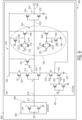
FIG. 7 depicts a modified level shifter circuit configuration in which additional circuit components are incorporated to protect the level shifter circuit from damage due to electrical discharge occurring during device fabrication.FIG. 7 depicts theSOC device 600 ofFIG. 6 modified by the incorporation of additional circuit elements to formSOC device 700 configured to provide electrical discharge protection. To the extent components inSOC device 700 are the same as those depicted inFIG. 6 (i.e., configured in the same manner and providing the same functionality), component element numbers are unchanged and the pertinent description of such components above is applicable. - As depicted,
SOC device 700 includes abypass path 702 that is connected betweeninput terminal 616 of the inverter formed bytransistors output terminal 618.Bypass path 702 includespass transistor 704. An input terminal oftransistor 704 is connected to input terminal 616.Bypass path 702 includesinverter 706. An input terminal ofinverter 706 is connected to an output terminal oftransistor 704.Bypass path 702 includespass transistor 708. An input terminal ofpass transistor 708 is connected to an output terminal ofinverter 706. An output terminal ofpass transistor 708 is connected tooutput terminal 618. - The control terminals of
pass transistors pass transistors - During device fabrication,
pass transistor 704 operate to protecttransistors input terminal 616 that may occur during fabrication steps involving plasma operations. This results because if the electrical discharge reaches a significant value (e.g., one that may cause damage to any oftransistors 612 and 614), the clamp diode configuration ofpass transistors 704 can cause that electrical discharge to be passed to ground. If, however, that electrical discharge does cause damage to one or more oftransistors present SOC device 700 configuration. - Specifically,
SOC device 700 includes a pair oftransistors transistors Transistor 720 is connected betweenpower terminal 620 andtransistor 612. The control terminal oftransistor 720 receives an input signal SE.Transistor 722 is connected betweenground terminal 622 andtransistor 614. The control terminal oftransistor 722 receive an input signal SEB, which is the opposite of SE. - In this configuration, if the value of SE is high (indicating that
pass transistors transistors transistor 720 is turned off (due to the inversion at the control terminal of transistor 720) and, similarly,transistor 722 is turned off (due to the inverted control signal SEB being supplied at the control terminal). As such, with SE set to a high value, the inverter oftransistors transistors input terminal 616 passes throughpass transistor 704, is inverted byinverter 706, passes throughpass transistor 708 and is output atoutput terminal 618. In other words, when SE is set to a high level the inverter oftransistors bypass path 702 is enabled. Becausebypass path 702 includesinverter 706,bypass path 702 operates as an inverter to mimic the functionality of the inverter oftransistors - Given this structure, therefore it is possible to test the operation of the inverter of
transistors transistors transistors pass transistors inverter 706 operate to output atoutput terminal 618 the inverted value of the input signal received frominput terminal 616, when toggling the value of SE, the output atoutput terminal 618 should not change if the inverter is operating correctly (i.e., has not been damaged). Accordingly, using the circuit ofSOC device 700 not only do passtransistors output terminal 618 it is possible to detect that the inverter oftransistors transistors - In the event that damage is detected, the control signal may be set to a high value, in which case the inverter of
transistors transistors inverter 706 operate as an inverter. Although this may enable ongoing error-free operations ofSOC device 700, as mentioned above, the configuration ofpass transistors SOC device 700 at full clock-speeds. Accordingly, when bypassing the inverter the operational frequency ofSOC device 700 may be reduced. - In a similar manner,
SOC device 700 includes asecond bypass path 752 configured to provide electrical protection to the level-shifter 631 made up oftransistors Bypass path 752 includespass transistor 754. An input terminal oftransistor 754 is connected to input terminal 616 and the control terminal oftransistor 626 of level-shifter 631. -
Pass transistor 754 is formed withinisolated WELL 606 and has a clamp diode configuration in which a pair of diodes are connected between a ground terminal and the input and output terminals ofpass transistor 754. Specifically, during device fabrication,pass transistor 754 operates to protecttransistors 626 from electrical discharge from isolated WELL 604 and intoinput terminal 616 that may occur during fabrication steps involving plasma operations. This results because if the electrical discharge reaches a significant value (e.g., one that may cause damage to transistor 626), the clamp diode configuration ofpass transistor 754 can cause that electrical discharge to be passed to ground. - If, however, that electrical discharge does cause damage to
transistor 626, that damage can be detected using thepresent SOC device 700 configuration. - Specifically,
SOC device 700 includes a pair oftransistors shifter 631.Transistor 760 is connected betweentransistor 628 andtransistor 624. The control terminal oftransistor 760 is connected to a high input signal from a power terminal to act as a balancing transistor fortransistor 762.Transistor 762 is essentially required to cut-offtransistor 626 in the case of failure andtransistor 760 is used to balance the differential arm.Transistor 762 is connected betweentransistor 634 andtransistor 626. The control terminal oftransistor 762 receive an input signal SEB, which is the opposite of SE. - In this configuration, if the value of SE is high (indicating that
pass transistor 754 is operational), andtransistor 626 is cutoff from the level-shifter circuit by thetransistor 762 which is OFF when SE is high.Transistor 758, which is connected tooutput 636 throughtransistor 755, which is controlled by the control input SE, will now be in enabled state becausetransistor 754 is ON andtransistor 756 is OFF. In this configuration,transistor 758 will take over the functionality oftransistor 626. The gate control oftransistor 758 is also connected toelectrical connection 617 throughpass transistor 754. In normal operation, SE is low and SEB is high. So,transistor 758 is disabled in this level-shifter circuit andtransistor 626 is enabled by default in level-shifter circuit. In the case of PID,transistor 754 tries to protecttransistor 626 through its clamp diode. Thealternate path 752 can be switched ON by driving SE to high to access the presence of any damage. - Given this structure, therefore it is possible to test the operation of level-
shifter 631. By supplying a particular input and toggling the control signal SE it is possible to selectively enable and disable the operation of level-shifter 631 and, correspondingly,second bypass path 752. When toggling that control signal, if level-shifter 631 is operating correctly, the output at 642 should not change when the control signal is toggled. If the output does change, that indicates a malfunction, which could be due to damage within level-shifter 631 (e.g., at transistor 626), or, potentially, damage intransistor - In the event that damage is detected, the control signal may be set to a high value, in which case level-
shifter 631 is disabled and instead,second bypass path 752 is operational withtransistors SOC device 700, as mentioned above, the configuration ofpass transistor 754 may not enable operation ofSOC device 700 at full clock-speeds. Accordingly, when bypassing level-shifter 631, the operational frequency ofSOC device 700 may be reduced. - In another embodiment, the present disclosure provides a circuit for detection and mitigation of PID-induced failure in an isolation cell device. To illustrate,
FIG. 8 is a simplified depiction of aconventional SOC device 800 configured to implement an isolation cell device.SOC device 800 includes asubstrate 802 including isolated WELL 804 andisolated WELL 806.Device 808 is formed withinisolated WELL 804.Device 808 includes an electronic circuit (e.g., a transistor structure in combination with an antenna or antenna-like structure) that is susceptible to charge build-up during a plasma-based manufacturing process ofSOC device 800. -
Isolation cell 810 is formed withinisolated WELL 806.Isolation cell 810 includes a transistorpair including transistors power supply terminal 820 andground terminal 822.Transistors input terminal 816 and anoutput terminal 818.Input terminal 816 is connected todevice 808 viaelectrical connection 817 and to the gate terminals oftransistors Input terminal 816 receives an input signal A that represent the primary input ofisolation cell 810. -
Output terminal 818 is connected to input terminal 834 of the inverter made of up oftransistors power supply terminal 820 andground terminal 840. - In this configuration, when
isolation cell 810 is operational (discussed below), the input signal A is received at 816 is inverted byinverter 842, inverted again byinverter 844 and output atoutput terminal 846. - To control the operation of
isolation cell 810,isolation cell 810 includes asecond input terminal 824 configured to receive a second signal EN that determines whether theisolation cell 810 is enabled. That input signal is inverted by the inverter made up oftransistors isolation cell 810 is enabled, and if B has a low value,isolation cell 810 is disabled. The control signal B is supplied to the gate control terminal oftransistor 830, which is connected betweentransistor 814 andground terminal 822. The same supply signal B is supplied at the gate or control terminal oftransistor 832, which is connected betweenpower supply terminal 820 andoutput terminal 818. - When B has a high value (indicating
isolation cell 810 is enabled),transistor 830 is enabled allowing for normal operations of the inverter made up bytransistors transistor 832 is disabled. However, when B has a low value (indicating thatisolation cell 810 is disabled),transistor 830 is non-conductive, meaning that the inverter oftransistors transistor 832 is conductive so that the value atoutput terminal 818 is pulled high to the voltage at 820. That high value is inverted byinverter 844, so in this configured (i.e., withisolation cell 810 disabled), the output ofisolation cell 810 will always be a low value. - In this configuration, during fabrication of
SOC device 800 and, specifically, during fabrication processes that involve plasma-based operations (e.g., plasma etching and/or plasma deposition) there is a risk of electrical charge build-up within isolated WELL 804 anddevice 808. That electrical charge may be discharged throughconnection 817 intoisolation cell 810, resulting in potential damage toisolation cell 810. In a typical case, this electrical discharge may be likely to damage the gate oxide of the gate terminal oftransistor 814, which we be subjected to a majority of that electrical discharge. - To remedy these problems,
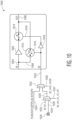
FIG. 9 depicts a modified isolation cell circuit configuration in which additional circuit components are incorporated to protect the isolation cell circuit from damage due to electrical discharge occurring during device fabrication.FIG. 9 depicts theSOC device 800 ofFIG. 8 modified by the incorporation of additional circuit elements to formSOC device 900 configured to provide electrical discharge protection. To the extent components inSOC device 900 are the same as those depicted inFIG. 8 (i.e., configured in the same manner and providing the same functionality), component element numbers are unchanged and the pertinent description of such components above is applicable. - As depicted,
SOC device 900 includes abypass path 902 or circuit including components that, as described below, can operate as a back-up inverter in the event of damage toinverter 842 and, specifically,transistors 814 ofinverter 842. - Specifically,
bypass path 902 includes aninverter 904 made oftransistors power supply terminal 820 and a first terminal oftransistor 830, as illustrated. -
Input terminal 910 is configured to receive the input signalA. Input terminal 910 is connected to first terminals oftransistors transistors transistor 906. The control terminal oftransistor 912 receives an input signal SEB, which is the inverse of the control signal SE, discussed below. The control terminal oftransistor 912 is an inverting input so when SEB is high,transistor 912 is non-conductive. However, when SEB is low,transistor 912 is conductive. The control terminal oftransistor 914 receives an input signal SE. When SE is high,transistor 914 is conductive. When SE is low,transistor 914 is conductive. - In this configuration, when SE is high, the input signal A is passed through
transistors transistor 906. -
Input terminal 920 is configured to receive the input signalA. Input terminal 920 is connected to first terminals oftransistors transistors transistor 908. The control terminal oftransistor 924 receives an input signal SEB, which is the inverse of the control signal SE. The control terminal oftransistor 924 is an inverting input so when SEB is high,transistor 924 is non-conductive. However, when SEB is low,transistor 924 is conductive. The control terminal oftransistor 922 receives an input signal SE. When SE is high,transistor 922 is conductive. When SE is low,transistor 922 is conductive. - In this configuration, when SE is high, the input signal A is passed through
transistors transistor 908. -
Transistor 926 is connected betweenpower supply terminal 820 and the control terminal oftransistor 906. The control signal SE is supplied to the control terminal oftransistor 926, which is an inverting terminal. As such, when SE is high,transistor 926 is non-conductive, enabling operation ofbypass path 902. However, when SE is low (e.g., during normal operations ofSOC device 900 in which bypasspath 902 is non-operative),transistor 926 is conductive, which connects the control terminal oftransistor 906 topower supply terminal 820, which, due to the transistor's inverting control terminal makestransistor 906 non-conductive, effectively disablingbypass path 902. - Similarly,
transistor 928 is connected between the control terminal oftransistor 906 andground node 930. The control signal SEB is supplied to the control terminal oftransistor 928. As such, when SEB is low,transistor 928 is non-conductive, enabling operation ofbypass path 902. However, when SEB is high (e.g., during normal operations ofSOC device 900 in which bypasspath 902 is non-operative),transistor 928 is conductive, which connects the control terminal oftransistor 908 toground node 930, which makestransistor 908 non-conductive, effectively disablingbypass path 902. -
Transistor 932 is connected between a first terminal oftransistor 812 andpower supply terminal 820. The control terminal oftransistor 932 receives the SE control input signal. The control terminal oftransistor 932 is an inverting terminal such that when SE is high,transistor 932 is non-conductive, which disables the operation ofinverter 842. Conversely, when SE is low,transistor 932 is conductive enabling normal operations ofinverter 842. -
Transistor 934 is connected betweentransistor 814 andtransistor 830. The control terminal oftransistor 934 receives the SEB control input signal. When SE is low,transistor 934 is non-conductive, which disables the operation ofinverter 842. Conversely, when SEB is high,transistor 934 is conductive enabling normal operations ofinverter 842. - In this configuration, if the value of SE is low (indicating that
inverter 842 is operational),inverter 904 ofbypass path 902 is disabled andisolation cell 810 can operate normally. However, if the value of SE is high,inverter 842 is effectively disabled, andbypass path 902 is enabled such thatinverter 904 supplies the inverted version of input signal A toinput terminal 834 ofinverter 844. - Given this structure, therefore it is possible to test the operation of
inverter 842 to detect potential damage that may have resulted during plasma processing, as discussed above. As such, by supplying particular input signals A and EN and toggling the control signal SE it is possible to selectively enable and disable the operation ofinverter 842 and, correspondingly,transistors output terminal 846 should not change ifinverter 842 is operating correctly (i.e., has not been damaged). Accordingly, using the circuit ofSOC device 900, by toggling the value of control signal SE and monitoring the signal atoutput terminal 846 it is possible to detect thatinverter 842 is not operating correctly (e.g., as an inverter), which can be an indication of damage, which may be due to electrical discharge, for example, into the gate terminal of one or more oftransistors - In the event that damage is detected, the control signal SE may be set to a high value, in which
case inverter 842 is disabled and instead, bypasspath 902 operates as an inverter to enable ongoing error-free operations ofSOC device 900. -
FIG. 10 is a block diagram depicting functional components of adevice 1000 configured in accordance with the present disclosure.Device 1000 includes an electronic device 1002 (e.g., a buffer, inverter, level shifter, or isolation cell) that includes aninput terminal 1004 and anoutput terminal 1006.Device 1000 includes a bypass path 1008 (e.g.,bypass path 302,bypass path 502,bypass path 702,second bypass path 752, bypass path 902) that is connected betweeninput terminal 1004 andoutput terminal 1006.Bypass path 1008 includes switch 1010 (e.g.,pass transistor 304, passtransistors 504,pass transistor 704, pass transistor 754) that is controlled by a control signal received atcontrol input 1012 ofswitch 1010. When the control signal has a first value,switch 1010 is open, which disablesbypass path 1008 enabling normal operation ofelectronic device 1002. However, when the control signal has a second value,switch 1010 is closed, enablingbypass path 1008 and effectively bypassingelectronic device 1002. -
Device 1000 includes switch 1014 (e.g.,transistor 320 andtransistor 322,transistor 520 andtransistor 522,transistor 760 andtransistor 762, bypass path 902) that is controlled by a control signal received atcontrol input 1016 ofswitch 1014. The control signal received bycontrol input 1016 ofswitch 1014 is inverted byinverter 1018 so that when the control signal has the first value,switch 1010 is closed, which enables the output ofelectronic device 1002 to be passed tooutput terminal 1006. However, when the control signal has the second value,control input 1016 is open, disconnectingelectronic device 1002 fromoutput terminal 1006 effectively disablingelectronic device 1002. - The control signal is received at
control signal input 1020 as an output fromdemultiplexer 1022.Demultiplexer 1022 has afirst input 1024 configured to receive an input based on the device configuration. Asecond input 1026 ofdemultiplexer 1022 is configured to receive an output fromdemultiplexer 1030.Demultiplexer 1022 receives a control input atcontrol terminal 1028. When the input atcontrol terminal 1028 causes the input signal atfirst input 1024 to be output bydemultiplexer 1022, the value of the control signal can be determined by the Fuse Bit or NVM bit. However, when the input atcontrol terminal 1028 causes the input signal atsecond input 1026 to be output bydemultiplexer 1022, the value of the control signal can be determined by the output signal ofdemultiplexer 1030. -
Demultiplexer 1030 includes afirst input 1032 configured to receive an input from a device test data register.Demultiplexer 1030 includes asecond input 1034 configured to receive an input from adevice pin 1036 or other electrical terminal accessible to external devices. The output ofsecond input 1034 is determined by a control signal received atcontrol input 1037, which selects whether the output ofsecond input 1034 is the value stored in the test data register or the value at thedevice pin 1036. - As such, by selecting appropriate input signals to
demultiplexer 1022 anddemultiplexer 1030,device 1000 may be placed in a normal mode of operation (e.g., where the output ofcontrol signal input 1020 is the first value of the control signal). In that case,bypass path 1008 is disabled. - However, by providing different inputs to
demultiplexer 1022 anddemultiplexer 1030, the control signal can be set to the second value (e.g., via one or more input of the Fuse bit, the test data register, or the external control pin) enablingbypass path 1008 to be enabled and, at the same time,electronic device 1002 to be disabled. - Accordingly,
demultiplexer 1022 anddemultiplexer 1030 provide various mechanisms by whichbypass path 1008 can be selectively enabled to allow for test patterns to be executed onelectronic device 1002 to detect potential malfunctions, such as those resulting from plasma induced discharge. - To illustrate,
FIG. 11 is a flow chart depicting amethod 1100 of testing an SOC device incorporating a bypass circuit configured in accordance with the present disclosure to detect potential device damage.Method 1100 may be implemented by a suitably configured testing device configured to provide signal inputs and control signals (e.g., the signals SE and/or SEB) to various input terminals of the SOC device being tested.Method 1100 begins atblock 1102. To initiate testing, atblock 1104 the select control signal SE is driven to a low value of 0 (e.g., to disable the various bypass circuits and enable normal operations of the device). At block 1106 a series of automatic test pattern generator (ATPG) test patterns are run to determine whether the device is operating correctly. If, atpass block 1108, it is determined that the device passes the ATPG test patterns with SE set to a high value,method 1100 ends atblock 1110 with an indication that there is no PID issue and that the device is not malfunctioning. - If, however, at
block 1108 it is determined that the device did not pass the ATPG test pattern with SE set to a low value, atblock 1112 the control input SE is set to a high value of 1 and the same ATPG test patterns are run atblock 1114. - If at
block 1116 it is determined that the device passed the ATPG test patterns,method 1100 ends atblock 1118 with an indication that there are no PID issues. In that case, the device may operate normally, however, as discussed above, because the device is operating nominally only due to the use of the various bypass paths or circuits described herein (as enabled by the high SE control signal input), the device may be configured to operate at a reduced operational frequency. This outcome is indicative of detection of a potential PID issue with the device. - If, however, at
block 1116 it is determined that the device again failed the ATPG test patterns, the method ends atblock 1120 with an indication that the device has a potential non-PID related issue that requires diagnosis. - A system and method for electronic device damage detection is presented. A first input signal is supplied to an input terminal of an electronic device. The electronic device includes a input terminal, a first electronic circuit including a first transistor, wherein a control terminal of the first transistor is electrically connected to the input terminal, a second electronic circuit including a clamp diode transistor, wherein the clamp diode is electrically connected to the input terminal, wherein the clamp diode transistor is configured to receive a control input signal and when the control input signal has a first value the clamp diode transistor is conductive, and an output terminal electrically connected to the first electronic circuit and the second electronic circuit. The control input signal is switched between the first value and a second value and an output of the electronic device is monitored to detect a malfunction.
- In some aspects, the techniques described herein relate to a device, including: a substrate that includes a first isolated well and a second isolated well; a first electronic device formed within the first isolated well, the first electronic device including a first electronic circuit electrically connected to an antenna; and a second electronic device formed within the second isolated well, the second electronic device including: an input terminal that is electrically connected to the first electronic device, a second electronic circuit, the second electronic circuit including a first transistor, wherein a control terminal of the first transistor is electrically connected to the input terminal, a third electronic circuit including a clamp diode transistor, wherein the clamp diode is electrically connected to the input terminal, wherein the clamp diode transistor is configured to limit a voltage that may be applied to the control terminal of the first transistor and wherein the clamp diode transistor is configured to receive a control input signal, wherein when the control input signal has a first value the clamp diode transistor is conductive, and an output terminal electrically connected to the second electronic circuit and the third electronic circuit.
- In some aspects, the techniques described herein relate to a system, including: a device, including: a substrate that includes an isolated well, an electronic device within the isolated well, the electronic device including: an input terminal, a first electronic circuit including a first transistor, wherein a control terminal of the first transistor is electrically connected to the input terminal, a second electronic circuit including a clamp diode transistor, wherein the clamp diode is electrically connected to the input terminal, wherein the clamp diode transistor is configured to receive a control input signal and when the control input signal has a first value the clamp diode transistor is conductive, and an output terminal electrically connected to the first electronic circuit and the second electronic circuit; and a testing device configured to perform steps of: supplying a first input signal to the input terminal, switching the control input signal between the first value and a second value, and monitoring an output of the electronic device at the output terminal to detect a malfunction in the electronic device.
- In some embodiments, the first electronic circuit is configured to receive the control input signal and wherein, when the control input signal has the first value, the first electronic circuit is disabled. In some embodiments the testing device, to detect the malfunction in the second electronic device, is configured to perform steps of: when the control input signal has the first value, detect a first output value of an output signal of the electronic device at the output terminal; when the control input signal has the second value, detect a second output value of an output signal of the electronic device at the output terminal; and determine that the first output value is not equal to the second output value.
- In some embodiments, the testing device, to detect the malfunction in the second electronic device, is configured to perform steps of: setting the control input signal to the first value; determining a first result of a set of ATPG test patterns run on the second electronic device; setting the control input signal to the second value; determining a second result of the set of ATPG test patterns run on the second electronic device; and detecting the malfunction based on at least one of the first result and the second result. In some embodiments, the testing device, after detecting the malfunction, is configured to generate an output indicative of a plasma induced damage to the second electronic device.
- In some embodiments, the second electronic circuit includes an input buffer and wherein a first terminal of the clamp diode transistor is connected to the input terminal, a second terminal of the clamp diode transistor is connected to the output terminal, and a control terminal of the clamp diode transistor is configured to receive the control input signal. In some embodiments, the device includes a wireless signal receiver and the electronic device includes a signal driver.
- In some aspects, the techniques described herein relate to a method, including: supplying a first input signal to an input terminal of an electronic device, wherein the electronic device includes: a substrate that includes an isolated well, a electronic device within the isolated well, the electronic device including: the input terminal, a first electronic circuit including a first transistor, wherein a control terminal of the first transistor is electrically connected to the input terminal, a second electronic circuit including a clamp diode transistor, wherein the clamp diode is electrically connected to the input terminal, wherein the clamp diode transistor is configured to receive a control input signal and when the control input signal has a first value the clamp diode transistor is conductive, and an output terminal electrically connected to the first electronic circuit and the second electronic circuit; switching the control input signal between the first value and a second value; and monitoring an output of the electronic device at the output terminal to detect a malfunction in the electronic device.
- Because the apparatus implementing the present invention is, for the most part, composed of electronic components and circuits known to those skilled in the art, circuit details will not be explained in any greater extent than that considered necessary as illustrated above, for the understanding and appreciation of the underlying concepts of the present invention and in order not to obfuscate or distract from the teachings of the present invention.
- Moreover, the terms "front," "back," "top," "bottom," "over," "under" and the like in the description and in the claims, if any, are used for descriptive purposes and not necessarily for describing permanent relative positions. It is understood that the terms so used are interchangeable under appropriate circumstances such that the embodiments of the invention described herein are, for example, capable of operation in other orientations than those illustrated or otherwise described herein.
- As used herein the terms "substantial" and "substantially" mean sufficient to accomplish the stated purpose in a practical manner and that minor imperfections, if any, are not significant for the stated purpose. Also as used herein, the terms "approximately" and "about" mean a value close to or within an acceptable range of an indicated value, amount, or quality, which also includes the exact indicated value itself.
- Although the invention is described herein with reference to specific embodiments, various modifications and changes can be made without departing from the scope of the present invention as set forth in the claims below. Accordingly, the specification and figures are to be regarded in an illustrative rather than a restrictive sense, and all such modifications are intended to be included within the scope of the present invention. Any benefits, advantages, or solutions to problems that are described herein with regard to specific embodiments are not intended to be construed as a critical, required, or essential feature or element of any or all the claims.
- Furthermore, the terms "a" or "an," as used herein, are defined as one or more than one. Also, the use of introductory phrases such as "at least one" and "one or more" in the claims should not be construed to imply that the introduction of another claim element by the indefinite articles "a" or "an" limits any particular claim containing such introduced claim element to inventions containing only one such element, even when the same claim includes the introductory phrases "one or more" or "at least one" and indefinite articles such as "a" or "an." The same holds true for the use of definite articles.
- The following detailed description is merely illustrative in nature and is not intended to limit the embodiments of the subject matter or the application and uses of such embodiments. As used herein, the words "exemplary" and "example" mean "serving as an example, instance, or illustration." Any implementation described herein as exemplary or an example is not necessarily to be construed as preferred or advantageous over other implementations. Furthermore, there is no intention to be bound by any expressed or implied theory presented in the preceding technical field, background, or the following detailed description.
- For the sake of brevity, conventional semiconductor fabrication techniques may not be described in detail herein. In addition, certain terminology may also be used herein for reference only, and thus are not intended to be limiting, and the terms "first", "second" and other such numerical terms referring to structures do not imply a sequence or order unless clearly indicated by the context.
- The foregoing description refers to elements or nodes or features being "connected" or "coupled" together. As used herein, unless expressly stated otherwise, "connected" means that one element is directly joined to (or directly communicates with) another element, and not necessarily mechanically. Likewise, unless expressly stated otherwise, "coupled" means that one element is directly or indirectly joined to (or directly or indirectly communicates with) another element, and not necessarily mechanically. Thus, although the schematic shown in the figures depict one exemplary arrangement of elements, additional intervening elements, devices, features, or components may be present in an embodiment of the depicted subject matter.
- While at least one exemplary embodiment has been presented in the foregoing detailed description, it should be appreciated that a vast number of variations exist. It should also be appreciated that the exemplary embodiment or embodiments described herein are not intended to limit the scope, applicability, or configuration of the claimed subject matter in any way. Rather, the foregoing detailed description will provide those skilled in the art with a convenient road map for implementing the described embodiment or embodiments. It should be understood that various changes can be made in the function and arrangement of elements without departing from the scope defined by the claims, which includes known equivalents and foreseeable equivalents at the time of filing this patent application.
Claims (13)
- A device, comprising:a substrate that includes a first isolated well and a second isolated well;a first electronic device formed within the first isolated well, the first electronic device including a first electronic circuit electrically connected to an antenna; anda second electronic device formed within the second isolated well, the second electronic device including:an input terminal that is electrically connected to the first electronic device,a second electronic circuit, the second electronic circuit including a first transistor, wherein a control terminal of the first transistor is electrically connected to the input terminal,a third electronic circuit including a clamp diode transistor, wherein the clamp diode is electrically connected to the input terminal, wherein the clamp diode transistor is configured to limit a voltage that may be applied to the control terminal of the first transistor and wherein the clamp diode transistor is configured to receive a control input signal, wherein when the control input signal has a first value the clamp diode transistor is conductive, andan output terminal electrically connected to the second electronic circuit and the third electronic circuit.
- The device of claim 1, wherein the second electronic circuit is configured to receive the control input signal and wherein, when the control input signal has the first value, the second electronic circuit is disabled.
- The device of claim 2, wherein the second electronic circuit includes a second transistor and wherein a control terminal of the second transistor is configured to receive the control input signal.
- The device of claim 2 or 3, further comprising a testing device configured to perform steps of:supplying a first input signal to the input terminal;switching the control input signal between the first value and a second value, andmonitoring an output of the second electronic device at the output terminal to detect a malfunction in the second electronic device.
- The device of claim 4, wherein the testing device, to detect the malfunction in the second electronic device, is configured to perform steps of:when the control input signal has the first value, detect a first output value of an output signal of the second electronic device at the output terminal;when the control input signal has the second value, detect a second output value of an output signal of the second electronic device at the output terminal; anddetermine that the first output value is not equal to the second output value.
- The device of claim 4 or 5, wherein the testing device, to detect the malfunction in the second electronic device, is configured to perform steps of:setting the control input signal to the first value;determining a first result of a set of ATPG test patterns run on the second electronic device;setting the control input signal to the second value;determining a second result of the set of ATPG test patterns run on the second electronic device; anddetecting the malfunction based on at least one of the first result and the second result.
- The device of any of claims 4 to 6, wherein the testing device, after detecting the malfunction, is configured to generate an output indicative of a plasma induced damage to the second electronic device.
- The device of any preceding claim, wherein the second electronic circuit includes an input buffer and wherein a first terminal of the clamp diode transistor is connected to the input terminal, a second terminal of the clamp diode transistor is connected to the output terminal, and a control terminal of the clamp diode transistor is configured to receive the control input signal.
- The device of any preceding claim, wherein the first electronic device includes a wireless signal receiver and the second electronic device includes a signal driver.
- A method, comprising:supplying a first input signal to an input terminal of an electronic device, wherein the electronic device includes:a substrate that includes an isolated well,a electronic device within the isolated well, the electronic device including:the input terminal,a first electronic circuit including a first transistor, wherein a control terminal of the first transistor is electrically connected to the input terminal,a second electronic circuit including a clamp diode transistor, wherein the clamp diode is electrically connected to the input terminal, wherein the clamp diode transistor is configured to receive a control input signal and when the control input signal has a first value the clamp diode transistor is conductive, andan output terminal electrically connected to the first electronic circuit and the second electronic circuit;switching the control input signal between the first value and a second value; andmonitoring an output of the electronic device at the output terminal to detect a malfunction in the electronic device.
- The method of claim 10, further comprising detecting the malfunction in the second electronic device by performing steps including:when the control input signal has the first value, detecting a first output value of an output signal of the electronic device at the output terminal;when the control input signal has the second value, detecting a second output value of an output signal of the electronic device at the output terminal; anddetermining that the first output value is not equal to the second output value.
- The method of claim 10 or 11, further comprising detecting the malfunction in the second electronic device by performing steps including:setting the control input signal to the first value;determining a first result of a set of ATPG test patterns run on the second electronic device;setting the control input signal to the second value;determining a second result of the set of ATPG test patterns run on the second electronic device; anddetecting the malfunction based on at least one of the first result and the second result.
- The method of claim 12, further comprising, after detecting the malfunction, generating an output indicative of a plasma induced damage to the second electronic device.
Applications Claiming Priority (1)
| Application Number | Priority Date | Filing Date | Title |
|---|---|---|---|
| IN202341088819 | 2023-12-26 |
Publications (1)
| Publication Number | Publication Date |
|---|---|
| EP4580347A1 true EP4580347A1 (en) | 2025-07-02 |
Family
ID=93925343
Family Applications (1)
| Application Number | Title | Priority Date | Filing Date |
|---|---|---|---|
| EP24220777.7A Pending EP4580347A1 (en) | 2023-12-26 | 2024-12-17 | Circuit for detection and mitigation of device damage to an electronic device |
Country Status (2)
| Country | Link |
|---|---|
| US (1) | US20250210958A1 (en) |
| EP (1) | EP4580347A1 (en) |
Citations (4)
| Publication number | Priority date | Publication date | Assignee | Title |
|---|---|---|---|---|
| US6414358B1 (en) * | 2001-09-28 | 2002-07-02 | Intel Corporation | Arrangements to reduce charging damage in structures of integrated circuits |
| US20020130368A1 (en) * | 2001-03-13 | 2002-09-19 | Chin-Ping Tan | Method for protecting MOS components form antenna effect and the apparatus thereof |
| US20130256801A1 (en) * | 2012-03-28 | 2013-10-03 | Taiwan Semiconductor Manufacturing Company, Ltd. | Integrated circuit structure to resolve deep-well plasma charging problem and method of forming the same |
| US20220293597A1 (en) * | 2021-03-11 | 2022-09-15 | Taiwan Semiconductor Manufacturing Company Ltd. | Semiconductor and circuit structures, and related methods |
Family Cites Families (17)
| Publication number | Priority date | Publication date | Assignee | Title |
|---|---|---|---|---|
| US5416351A (en) * | 1991-10-30 | 1995-05-16 | Harris Corporation | Electrostatic discharge protection |
| US6078487A (en) * | 1992-03-31 | 2000-06-20 | Digital Equipment Corporation | Electro-static discharge protection device having a modulated control input terminal |
| US5917220A (en) * | 1996-12-31 | 1999-06-29 | Stmicroelectronics, Inc. | Integrated circuit with improved overvoltage protection |
| US6075686A (en) * | 1997-07-09 | 2000-06-13 | Industrial Technology Research Institute | ESD protection circuit for mixed mode integrated circuits with separated power pins |
| US6417544B1 (en) * | 2001-06-11 | 2002-07-09 | Chartered Semiconductor Manufacturing Ltd. | Diode-like plasma induced damage protection structure |
| DE10246098A1 (en) * | 2002-10-02 | 2004-04-22 | Epcos Ag | circuitry |
| US7817459B2 (en) * | 2007-01-24 | 2010-10-19 | Keystone Semiconductor Inc. | Depletion-mode MOSFET circuit and applications |
| US8525265B2 (en) * | 2010-02-12 | 2013-09-03 | United Microelectronics Corp. | Electrostatic discharge protection circuit |
| US9088224B2 (en) * | 2010-07-21 | 2015-07-21 | Lihua Chen | Variable voltage converter with stabilized output voltage |
| US8634174B2 (en) * | 2011-05-25 | 2014-01-21 | International Business Machines Corporation | Gate dielectric breakdown protection during ESD events |
| US20140268446A1 (en) * | 2013-03-15 | 2014-09-18 | Qualcomm Incorporated | Radio frequency integrated circuit (rfic) charged-device model (cdm) protection |
| US9466976B2 (en) * | 2013-05-15 | 2016-10-11 | Oeco, Llc | Active transient voltage suppression device |
| US20140376134A1 (en) * | 2013-06-19 | 2014-12-25 | Texas Instruments Incorporated | Voltage Protection Circuit |
| US10593661B2 (en) * | 2017-03-03 | 2020-03-17 | Texas Instruments Incorporated | Circuit overvoltage protection |
| EP3588559B1 (en) * | 2018-06-29 | 2021-10-20 | Intel Corporation | Circuit for electrostatic discharge protection for wide frequency range multi-band interfaces |
| US11469717B2 (en) * | 2019-05-03 | 2022-10-11 | Analog Devices International Unlimited Company | Microwave amplifiers tolerant to electrical overstress |
| US20230187435A1 (en) * | 2021-12-14 | 2023-06-15 | Skyworks Solutions, Inc. | Diode configuration for circuit protection |
-
2024
- 2024-02-14 US US18/441,013 patent/US20250210958A1/en active Pending
- 2024-12-17 EP EP24220777.7A patent/EP4580347A1/en active Pending
Patent Citations (4)
| Publication number | Priority date | Publication date | Assignee | Title |
|---|---|---|---|---|
| US20020130368A1 (en) * | 2001-03-13 | 2002-09-19 | Chin-Ping Tan | Method for protecting MOS components form antenna effect and the apparatus thereof |
| US6414358B1 (en) * | 2001-09-28 | 2002-07-02 | Intel Corporation | Arrangements to reduce charging damage in structures of integrated circuits |
| US20130256801A1 (en) * | 2012-03-28 | 2013-10-03 | Taiwan Semiconductor Manufacturing Company, Ltd. | Integrated circuit structure to resolve deep-well plasma charging problem and method of forming the same |
| US20220293597A1 (en) * | 2021-03-11 | 2022-09-15 | Taiwan Semiconductor Manufacturing Company Ltd. | Semiconductor and circuit structures, and related methods |
Also Published As
| Publication number | Publication date |
|---|---|
| US20250210958A1 (en) | 2025-06-26 |
Similar Documents
| Publication | Publication Date | Title |
|---|---|---|
| US9188645B2 (en) | System and method for testing a circuit | |
| US7816890B2 (en) | Semiconductor unit for protecting secondary battery, battery pack having the semiconductor unit built-in and electronic apparatus using it | |
| US20090009133A1 (en) | Battery state monitoring circuit and battery apparatus | |
| US20090001994A1 (en) | Semiconductor device including fuse and method for testing the same capable of suppressing erroneous determination | |
| US10896808B2 (en) | Maintenance mode power supply system | |
| US20090237846A1 (en) | Esd protection circuit and method thereof | |
| US8519730B2 (en) | Circuit, system, and method for degradation detection | |
| KR20070121010A (en) | Voltage fault detection and protection | |
| US10965118B2 (en) | Over voltage/energy protection apparatus | |
| KR100389172B1 (en) | Repair signal generating circuit | |
| KR20020067667A (en) | Battery state monitoring circuit | |
| US7573273B2 (en) | Fuse cutting test circuit, fuse cutting test method, and semiconductor circuit | |
| US20250210958A1 (en) | Circuit for detection and mitigation of device damage to an electronic device | |
| EP4711779A1 (en) | Level shifter circuit | |
| JP4535910B2 (en) | Secondary battery protection circuit, battery pack and electronic device | |
| US12424859B2 (en) | Charge control circuit, charge control device, and battery device | |
| US8363366B2 (en) | Electrostatic discharge protection circuit | |
| CN214622955U (en) | Protection circuits and test equipment | |
| US7800420B2 (en) | Power detection system and circuit for high voltage supply and low voltage devices | |
| KR100621626B1 (en) | Semiconductor test device using leakage current and compensation system of leakage current | |
| CN112147517B (en) | Battery pack detection device and system | |
| US7063988B1 (en) | Circuit for detecting arcing in an etch tool during wafer processing | |
| CN116896363B (en) | NMOS control circuit and battery protection chip | |
| US7224198B2 (en) | Input and output circuit and method of operation thereof | |
| CN220064244U (en) | Detection circuit and test equipment of leakage protector |
Legal Events
| Date | Code | Title | Description |
|---|---|---|---|
| PUAI | Public reference made under article 153(3) epc to a published international application that has entered the european phase |
Free format text: ORIGINAL CODE: 0009012 |
|
| STAA | Information on the status of an ep patent application or granted ep patent |
Free format text: STATUS: THE APPLICATION HAS BEEN PUBLISHED |
|
| AK | Designated contracting states |
Kind code of ref document: A1 Designated state(s): AL AT BE BG CH CY CZ DE DK EE ES FI FR GB GR HR HU IE IS IT LI LT LU LV MC ME MK MT NL NO PL PT RO RS SE SI SK SM TR |
|
| STAA | Information on the status of an ep patent application or granted ep patent |
Free format text: STATUS: REQUEST FOR EXAMINATION WAS MADE |
|
| 17P | Request for examination filed |
Effective date: 20260102 |
|
| GRAP | Despatch of communication of intention to grant a patent |
Free format text: ORIGINAL CODE: EPIDOSNIGR1 |
|
| STAA | Information on the status of an ep patent application or granted ep patent |
Free format text: STATUS: GRANT OF PATENT IS INTENDED |
|
| RIC1 | Information provided on ipc code assigned before grant |
Ipc: H10D 89/60 20250101AFI20260602BHEP |
|
| INTG | Intention to grant announced |
Effective date: 20260616 |
|
| RIN1 | Information on inventor provided before grant (corrected) |
Inventor name: BHOOSHAN, RISHI Inventor name: JAIN, VIGYAN Inventor name: GUPTA, SHILPA Inventor name: GUPTA, CHANDAN Inventor name: REBER, DOUGLAS MICHAEL |