EP4580336A1 - Gaa-feldeffekttransistoren mit asymmetrischen rückseitigen source- und oberseitigen drain-kontakten - Google Patents
Gaa-feldeffekttransistoren mit asymmetrischen rückseitigen source- und oberseitigen drain-kontakten Download PDFInfo
- Publication number
- EP4580336A1 EP4580336A1 EP24220194.5A EP24220194A EP4580336A1 EP 4580336 A1 EP4580336 A1 EP 4580336A1 EP 24220194 A EP24220194 A EP 24220194A EP 4580336 A1 EP4580336 A1 EP 4580336A1
- Authority
- EP
- European Patent Office
- Prior art keywords
- contact
- source
- drain
- gate
- transistor
- Prior art date
- Legal status (The legal status is an assumption and is not a legal conclusion. Google has not performed a legal analysis and makes no representation as to the accuracy of the status listed.)
- Pending
Links
Images






Classifications
-
- H—ELECTRICITY
- H10—SEMICONDUCTOR DEVICES; ELECTRIC SOLID-STATE DEVICES NOT OTHERWISE PROVIDED FOR
- H10D—INORGANIC ELECTRIC SEMICONDUCTOR DEVICES
- H10D30/00—Field-effect transistors [FET]
- H10D30/501—FETs having stacked nanowire, nanosheet or nanoribbon channels
-
- H—ELECTRICITY
- H10—SEMICONDUCTOR DEVICES; ELECTRIC SOLID-STATE DEVICES NOT OTHERWISE PROVIDED FOR
- H10D—INORGANIC ELECTRIC SEMICONDUCTOR DEVICES
- H10D30/00—Field-effect transistors [FET]
- H10D30/60—Insulated-gate field-effect transistors [IGFET]
- H10D30/601—Insulated-gate field-effect transistors [IGFET] having lightly-doped drain or source extensions, e.g. LDD IGFETs or DDD IGFETs
- H10D30/603—Insulated-gate field-effect transistors [IGFET] having lightly-doped drain or source extensions, e.g. LDD IGFETs or DDD IGFETs having asymmetry in the channel direction, e.g. lateral high-voltage MISFETs having drain offset region or extended drain IGFETs [EDMOS]
-
- H—ELECTRICITY
- H10—SEMICONDUCTOR DEVICES; ELECTRIC SOLID-STATE DEVICES NOT OTHERWISE PROVIDED FOR
- H10D—INORGANIC ELECTRIC SEMICONDUCTOR DEVICES
- H10D30/00—Field-effect transistors [FET]
- H10D30/01—Manufacture or treatment
- H10D30/019—Manufacture or treatment of FETs having stacked nanowire, nanosheet or nanoribbon channels
-
- H—ELECTRICITY
- H10—SEMICONDUCTOR DEVICES; ELECTRIC SOLID-STATE DEVICES NOT OTHERWISE PROVIDED FOR
- H10D—INORGANIC ELECTRIC SEMICONDUCTOR DEVICES
- H10D30/00—Field-effect transistors [FET]
- H10D30/40—FETs having zero-dimensional [0D], one-dimensional [1D] or two-dimensional [2D] charge carrier gas channels
- H10D30/43—FETs having zero-dimensional [0D], one-dimensional [1D] or two-dimensional [2D] charge carrier gas channels having one-dimensional [1D] charge carrier gas channels, e.g. quantum wire FETs or transistors having 1D quantum-confined channels
-
- H—ELECTRICITY
- H10—SEMICONDUCTOR DEVICES; ELECTRIC SOLID-STATE DEVICES NOT OTHERWISE PROVIDED FOR
- H10D—INORGANIC ELECTRIC SEMICONDUCTOR DEVICES
- H10D30/00—Field-effect transistors [FET]
- H10D30/60—Insulated-gate field-effect transistors [IGFET]
- H10D30/62—Fin field-effect transistors [FinFET]
-
- H—ELECTRICITY
- H10—SEMICONDUCTOR DEVICES; ELECTRIC SOLID-STATE DEVICES NOT OTHERWISE PROVIDED FOR
- H10D—INORGANIC ELECTRIC SEMICONDUCTOR DEVICES
- H10D30/00—Field-effect transistors [FET]
- H10D30/60—Insulated-gate field-effect transistors [IGFET]
- H10D30/62—Fin field-effect transistors [FinFET]
- H10D30/6219—Fin field-effect transistors [FinFET] characterised by the source or drain electrodes
-
- H—ELECTRICITY
- H10—SEMICONDUCTOR DEVICES; ELECTRIC SOLID-STATE DEVICES NOT OTHERWISE PROVIDED FOR
- H10D—INORGANIC ELECTRIC SEMICONDUCTOR DEVICES
- H10D30/00—Field-effect transistors [FET]
- H10D30/60—Insulated-gate field-effect transistors [IGFET]
- H10D30/67—Thin-film transistors [TFT]
- H10D30/6729—Thin-film transistors [TFT] characterised by the electrodes
- H10D30/673—Thin-film transistors [TFT] characterised by the electrodes characterised by the shapes, relative sizes or dispositions of the gate electrodes
- H10D30/6735—Thin-film transistors [TFT] characterised by the electrodes characterised by the shapes, relative sizes or dispositions of the gate electrodes having gates fully surrounding the channels, e.g. gate-all-around
-
- H—ELECTRICITY
- H10—SEMICONDUCTOR DEVICES; ELECTRIC SOLID-STATE DEVICES NOT OTHERWISE PROVIDED FOR
- H10D—INORGANIC ELECTRIC SEMICONDUCTOR DEVICES
- H10D30/00—Field-effect transistors [FET]
- H10D30/60—Insulated-gate field-effect transistors [IGFET]
- H10D30/67—Thin-film transistors [TFT]
- H10D30/6757—Thin-film transistors [TFT] characterised by the structure of the channel, e.g. transverse or longitudinal shape or doping profile
-
- H—ELECTRICITY
- H10—SEMICONDUCTOR DEVICES; ELECTRIC SOLID-STATE DEVICES NOT OTHERWISE PROVIDED FOR
- H10D—INORGANIC ELECTRIC SEMICONDUCTOR DEVICES
- H10D62/00—Semiconductor bodies, or regions thereof, of devices having potential barriers
- H10D62/10—Shapes, relative sizes or dispositions of the regions of the semiconductor bodies; Shapes of the semiconductor bodies
- H10D62/117—Shapes of semiconductor bodies
- H10D62/118—Nanostructure semiconductor bodies
- H10D62/119—Nanowire, nanosheet or nanotube semiconductor bodies
- H10D62/121—Nanowire, nanosheet or nanotube semiconductor bodies oriented parallel to substrates
-
- H—ELECTRICITY
- H10—SEMICONDUCTOR DEVICES; ELECTRIC SOLID-STATE DEVICES NOT OTHERWISE PROVIDED FOR
- H10D—INORGANIC ELECTRIC SEMICONDUCTOR DEVICES
- H10D64/00—Electrodes of devices having potential barriers
- H10D64/20—Electrodes characterised by their shapes, relative sizes or dispositions
- H10D64/23—Electrodes carrying the current to be rectified, amplified, oscillated or switched, e.g. sources, drains, anodes or cathodes
- H10D64/251—Source or drain electrodes for field-effect devices
- H10D64/256—Source or drain electrodes for field-effect devices for lateral devices wherein the source or drain electrodes are recessed in semiconductor bodies
-
- H—ELECTRICITY
- H10—SEMICONDUCTOR DEVICES; ELECTRIC SOLID-STATE DEVICES NOT OTHERWISE PROVIDED FOR
- H10D—INORGANIC ELECTRIC SEMICONDUCTOR DEVICES
- H10D64/00—Electrodes of devices having potential barriers
- H10D64/20—Electrodes characterised by their shapes, relative sizes or dispositions
- H10D64/23—Electrodes carrying the current to be rectified, amplified, oscillated or switched, e.g. sources, drains, anodes or cathodes
- H10D64/251—Source or drain electrodes for field-effect devices
- H10D64/256—Source or drain electrodes for field-effect devices for lateral devices wherein the source or drain electrodes are recessed in semiconductor bodies
- H10D64/2565—Source or drain electrodes for field-effect devices for lateral devices wherein the source or drain electrodes are recessed in semiconductor bodies wherein the source or drain regions are on a top side of the semiconductor bodies and the recessed source or drain electrodes are on a bottom side of the semiconductor bodies
-
- B—PERFORMING OPERATIONS; TRANSPORTING
- B82—NANOTECHNOLOGY
- B82Y—SPECIFIC USES OR APPLICATIONS OF NANOSTRUCTURES; MEASUREMENT OR ANALYSIS OF NANOSTRUCTURES; MANUFACTURE OR TREATMENT OF NANOSTRUCTURES
- B82Y10/00—Nanotechnology for information processing, storage or transmission, e.g. quantum computing or single electron logic
Definitions
- the source and drain regions of transistors include electrical contacts to enable electrical connections to be formed to and from the transistors.
- larger contact sizes reduce resistance, which improves performance.
- parasitic capacitance may increase.
- the distance between the trenches of the source/drain contacts and the gate contact decreases.
- parasitic capacitance increases, which may lead to a higher propensity for shorting, thus reducing process yield.
- larger source/drain contacts reduce resistance, they can also increase parasitic capacitance if they become too large, which may negate the performance gains from lower resistance.
- the source and drain regions of transistors include electrical contacts to enable electrical connections to be formed to and from the transistors. These contacts are symmetrical and are formed on the frontside of an integrated circuit (e.g., above the source and drain). In general, larger contact sizes (e.g., wider, more contact area) are often preferable as they achieve lower resistance, which can improve performance. If the source and drain contacts are too large, however, parasitic capacitance may increase. For example, as the size of the source/drain contacts increases, the distance between the trenches of the source/drain contacts and the gate contact decreases. If the source/drain contacts and the gate contact become too close to each other, parasitic capacitance increases, which may lead to a higher propensity for shorting, thus reducing process yield. Thus, while larger source/drain contacts reduce resistance, they can also increase parasitic capacitance if they become too large, which may negate the performance gains from lower resistance.
- this disclosure presents embodiments of semiconductor devices (e.g., integrated circuits) with asymmetric transistor source and drain contacts, along with methods of forming the same.
- one of the source or drain contacts may be formed on the frontside of the semiconductor device (e.g., above the source or drain), and the other may be formed on the backside (e.g., below the source or drain).
- the frontside contact may be the standard or usual size to avoid interfering with the gate/gate contact, but the backside contact may have a larger size (e.g., wider, more contact area) since gate interference is not a concern on the backside.
- the backside contact size can be increased significantly without a capacitance penalty, such as by increasing the width and/or contact area of the backside contact relative to the frontside contact.
- the larger backside contact can be either the source contact or the drain contact depending on the performance implications in different embodiments. For example, if the source-side resistance is more dominant than drain-side resistance (e.g., due to a low bias on the source and a high bias on the drain), then the larger backside contact may be used for the source and the standard frontside contact may be used for the drain. Alternatively, if the opposite is true, then the larger backside contact may be used for the drain and the standard frontside contact may be used for the source.
- this solution increases performance due to the lower access resistance provided by the larger backside source or drain contact. Moreover, since there is no backside gate contact, there is no meaningful increase in parasitic capacitance due to the larger backside source/drain contact, nor any increased propensity for shorting.
- the lower contact resistance without a capacitance penalty improves transistor performance and enables cell height scaling, which results in faster microprocessors and improved process technology.
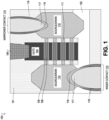
- FIG. 1 illustrates an example of a transistor 100 with asymmetric source and drain contacts.
- one of the source/drain contacts 114 is on the frontside of the transistor 100 and the other source/drain contact 112 is on the backside of the transistor 100.
- the backside contact 112 has a larger width and contact area than the frontside contact 114, which reduces resistance on the backside contact 112 without increasing parasitic capacitance.
- the transistor 100 may be part of a semiconductor device such as an integrated circuit.
- the transistor 100 is a nanoribbon transistor, where nanoribbons 108 are used as the transistor channel.
- the transistor 100 includes source and drain regions 110 formed over a substrate 102, nanoribbons 108 extending between the source/drain regions 110, and a gate 104 formed around the nanoribbons 108.
- the nanoribbons 108 couple the source/drain regions 110 and serve as the channel of the transistor 100.
- the tips/ends 111 of the nanoribbons 108 are doped with the same dopants as the source/drain regions 110, which causes the source/drain regions 110 to effectively extend or protrude into the tips 111 of the nanoribbons 108.
- the size of the backside contact 112 can be increased significantly relative to the frontside contact 114 without a capacitance penalty, thus reducing resistance.
- the backside (wider) contact 112 may have a width of -8-22 nanometers (nm)
- the frontside (narrower) contact 112 may have a width of ⁇ 6-16 nm
- the backside (wider) contact 112 may be ⁇ 2-6 nm wider than the frontside (narrower) contact 114.
- the backside (wider) contact 112 may be -10-40% wider than the frontside (narrower) contact 114.
- the materials used to form the respective layers may vary in different embodiments. Examples of materials that may be used for each layer are provided below.
- the substrate 102 may be made of any suitable material(s), including, without limitation, silicon.
- the inter-layer dielectric (ILD) 101 also referred to as an isolation oxide, may be made of any suitable dielectric material(s), including, without limitation, silicon dioxide (SiO 2 ) (and/or other oxides of silicon), silicon oxynitride (SiON), and/or silicon oxycarbide (SiOC).
- the ILD 101 may be made of material(s) that include elements such as silicon (Si), oxygen (O), nitrogen (N), and/or carbon (C).
- the gate 104 may be made of any suitable conductive or metal material(s), including, without limitation, titanium (Ti), titanium nitride (TiN), aluminum (Al), titanium aluminide (TiAl), titanium aluminum nitride (TiAIN), titanium silicon nitride (TiSiN), nickel (Ni), platinum (Pt), molybdenum (Mo), and/or tungsten (W).
- the gate 104 may be made of material(s) that include elements such as titanium (Ti), aluminum (Al), nickel (Ni), platinum (Pt), molybdenum (Mo), tungsten (W), nitrogen (N), and/or silicon (Si).
- the gate oxide 105 may be made of material(s) that include elements such as hafnium (Hf), silicon (Si), oxygen (O), nitrogen (N), zirconium (Zr), lanthanum (La), and/or tantalum (Ta).
- elements such as hafnium (Hf), silicon (Si), oxygen (O), nitrogen (N), zirconium (Zr), lanthanum (La), and/or tantalum (Ta).
- the source/drain contacts 112, 114 may be made of any suitable material(s), including those described below with respect to the contact metal 116, contact trench metal 117, and contact trench liner 118.
- the source/drain contact metal 116 may be made of material(s) that include elements such as titanium (Ti), aluminum (Al), nickel (Ni), platinum (Pt), molybdenum (Mo), tungsten (W), scandium (Sc), erbium (Er), yttrium (Y), ytterbium (Yb), gadolinium (Gd), terbium (Tb), dysprosium (Dy), and/or nitrogen (N).
- elements such as titanium (Ti), aluminum (Al), nickel (Ni), platinum (Pt), molybdenum (Mo), tungsten (W), scandium (Sc), erbium (Er), yttrium (Y), ytterbium (Yb), gadolinium (Gd), terbium (Tb), dysprosium (Dy), and/or nitrogen (N).
- the contact trench 117 may be made of any suitable conductive or metal material(s), including, without limitation, cobalt (Co), tungsten (W), molybdenum (Mo), aluminum (Al), and/or copper (Cu).
- Co cobalt
- W tungsten
- Mo molybdenum
- Al aluminum
- Cu copper
- the contact trench liner 118 may be made of any suitable dielectric material(s), including, without limitation, silicon oxynitride (SiON) and/or silicon oxycarbide (SiOC). Thus, in some embodiments, the contact trench liner 118 may be made of material(s) that include elements such as silicon (Si), oxygen (O), nitrogen (N), and/or carbon (C).
- transistor 100 may be implemented using other types, numbers, and/or arrangements of layers and materials than those shown and described with respect to FIG. 1 .
- the size and/or materials of the layers may vary.
- certain components of transistor 100 may be added, replaced, omitted, and/or rearranged.
- the substrate 102 may not be present in some embodiments, as it may be completely grinded/thinned away during fabrication.
- the frontside source/drain contact may be the larger contact if the gate is formed on the backside instead of the frontside.
- transistor 100 is a nanoribbon transistor
- asymmetric source/drain contacts can be implemented on any type of transistor, including nanoribbon transistors, gate-all-around (GAA) transistors, fin field-effect transistors (FinFET), planar transistors, and two-dimensional (2D) transistors (e.g., made of 2D semiconductor materials), among others.
- GAA gate-all-around
- FinFET fin field-effect transistors
- 2D transistors e.g., made of 2D semiconductor materials
- transistors with asymmetric source/drain contacts may be used for power delivery or signaling on semiconductor devices such as integrated circuits.
- transistors with asymmetric source/drain contacts may be used for backside power delivery (e.g., IC 300), where the backside source/drain contact is larger than the frontside source/drain contact, and power delivery is provided from the backside of the device.
- the narrower frontside contact may be coupled to a frontside interconnect, while the wider backside contact may be coupled to a backside interconnect.
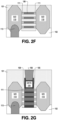
- FIGS. 2A-I illustrate an example process flow for forming a transistor 100 with asymmetric source and drain contacts.
- the process flow is used to form the transistor 100 of FIG. 1 . It will be appreciated in light of the present disclosure that the illustrated process flow is only one example methodology for arriving at a transistor with asymmetric source/drain contacts.
- a substrate 102 is received.
- the substrate 102 may be a silicon substrate.
- a superlattice with alternating silicon germanium (SiGe) 107 and silicon (Si) 108 layers is formed over the substrate 102.
- the Si layers 107 are the nanoribbons that will serve as the channel of the transistor 100 once complete.
- the SiGe/Si superlattice layers 107, 108 are etched away in the areas 109 where the respective source and drain regions 110 will be formed.
- a sacrificial dummy backside contact 113 is formed for one of the source or drain regions 110, which will subsequently be replaced with the actual backside contact during backside processing (e.g., as described below with respect to FIG. 2I ).
- the source and drain regions 110 are epitaxially grown. Further, the tips 111 of the silicon nanoribbons 108 are doped, which effectively causes the source and drain regions 110 to extend into the nanoribbons 108.
- the SiGe layers 107 are removed (e.g., etched) to release the nanoribbons 107.
- the gate oxide/dielectric 105 is formed over/around the released nanoribbon channels 108, and the gate 104 is then formed over/around the gate oxide 105 and nanoribbon channels 108.
- the gate contact 106 is then formed above/over the gate 104.
- any remaining frontside processing may be performed (not shown), such as frontside metallization/interconnect patterning.
- a carrier substrate may be attached to the top of the device (not shown), the device may be flipped, and the original substrate 102 may be grinded/thinned before performing backside processing (e.g., to expose the dummy contact along with any other backside connections).
- the dummy contact 113 is removed (e.g., etched) and the wider backside contact 112 is formed in its place.
- the backside contact 112 may be formed under the other one of the source or drain regions 110 and may include a contact metal 116, a contact trench metal 117, and a contact trench liner 118.
- the backside contact 112 is formed with a larger width and contact area than the frontside contact 114, thus reducing resistance and increasing performance.
- any remaining backside or other processing may be performed to complete the device (not shown), such as backside metallization/interconnect patterning.
- FIG. 3 illustrates a cross-section of an integrated circuit (IC) 300 with asymmetric transistor contacts in accordance with certain embodiments.
- IC 300 includes a layer 304 of transistors 305, and at least some of the transistors 305 have asymmetric source and drain contacts (e.g., different contact widths and/or contact areas).
- IC 300 includes a thinned silicon substrate 302, a device layer 304 over the silicon substrate 302, a frontside interconnect 306 over the device layer 304, and a backside interconnect 308 under the device layer 304 and the silicon substrate 302.
- IC 300 also includes a carrier substrate 301 attached above the frontside interconnect 306 for structural support, along with conductive (e.g., metal) bumps 303 on the bottom surface to electrically couple IC 300 with another electronic device (e.g., an IC package, another IC die/chip, etc.).
- conductive e.g., metal
- the device layer 304 includes one or more transistors 305 and/or other semiconductor devices. Moreover, at least some of the transistors 305 have asymmetric source and drain contacts. In some embodiments, for example, the transistors 305 may be implemented using the design of transistor 100. For example, transistors 305 with asymmetric contacts may have one contact on the frontside of IC 300 (e.g., above the source or drain) and another contact on the backside of IC 300 (e.g., below the other of the source or drain). In the illustrated embodiment, for example, some of the transistors 305 are shown with connections 315 to the backside source or drain contact. Moreover, the contact on the backside may have greater width and/or contact area than the contact on the frontside, as described throughout this disclosure.
- film deposition- such as depositing layers, filling portions of layers (e.g., removed portions), and filling via openings-may be performed using any suitable deposition techniques, including, for example, chemical vapor deposition (CVD), metal-organic chemical vapor deposition (MOCVD), molecular beam epitaxy (MBE), atomic layer deposition (ALD), and/or physical vapor deposition (PVD).
- CVD chemical vapor deposition
- MOCVD metal-organic chemical vapor deposition
- MBE molecular beam epitaxy
- ALD atomic layer deposition
- PVD physical vapor deposition
- patterning and removal- such as interconnect patterning, forming via openings, and shaping-may be performed using any suitable techniques, such as lithography-based patterning/masking and/or etching.
- the illustrated process flow may be used to form one or more IC dies that respectively include a device layer along with frontside and backside interconnects above and below the device layer (e.g., for signaling and power delivery).
- the device layer and interconnects may collectively implement logic circuitry and associated signal, power, and ground nets on the respective IC dies.
- at least some of the transistors in the device layer may include asymmetric source and drain contacts, as described throughout this disclosure.
- the flowchart begins at block 402 by receiving a first substrate.
- the first substrate may be a wafer or panel and may include silicon (Si). Further, the first substrate may be pre-patterned with one or more through-silicon vias (TSVs), or alternatively, the first substrate may be received without any pre-patterned TSVs and one or more TSVs may be subsequently formed in the substrate.
- TSVs through-silicon vias
- the transistors may be designed with asymmetric source and drain contacts, where one of the contacts is on the frontside of the first substrate (e.g., above the source or drain) and the other contact is on the backside of the first substrate (e.g., below the other of the source or drain), and the respective frontside/backside contacts have different widths and/or contact areas.
- the frontside contacts may have a smaller width and/or smaller contact area than the backside contacts (e.g., due to the presence of the gate on the frontside but not the backside).
- the frontside source or drain contacts are formed at block 404, while the backside source or drain contacts are formed at block 412, as described further below.
- dummy backside contacts may be formed in a portion of the source or the drain to aid in forming the actual backside contacts at block 412.
- one or more vias may be formed through the device layer to form electrical connections to the TSVs in the first substrate.
- the flowchart then proceeds to block 406 to form a first interconnect over the device layer (e.g., on the frontside of the first substrate), which may be referred to as the frontside interconnect.
- the frontside interconnect For example, multiple conductive (e.g., metal) layers may be formed over the device layer, along with intervening dielectric layers separating the conductive layers.
- the conductive layers which may also be referred to as metal layers, may be made of one or more electrically-conductive materials that include one or more metals (e.g., any of the metals/alloys described throughout this disclosure).
- the dielectric layers may include one or more dielectric materials (e.g., any of the dielectric materials described throughout this disclosure).
- conductive traces may be patterned (e.g., etched) in the frontside conductive layers, and vias may be formed between the conductive layers (e.g., through the intervening dielectric layers) to electrically couple traces in different conductive layers.
- the conductive traces and vias patterned in and between the frontside conductive layers may collectively form one or more signal, power, and/or ground nets for the logic circuitry on the respective IC dies (e.g., networks of conductive traces that provide signaling, power, and ground connections).
- the signal nets may include one or more conductive traces used for signaling (e.g., electrical connections between inputs and outputs of devices/transistors in the device layer), which may also be referred to as signal traces or signal routing. Further, the signal nets in the frontside interconnect may be connected to one or more corresponding signal nets formed in the backside interconnect for off-die signal routing (e.g., as described below with respect to block 414).
- the power nets may include one or more conductive traces for delivering power (e.g., electrical connections between the device layer and one or more power supply terminals), which may also be referred to as power traces or power routing. Further, the power nets in the frontside interconnect may be connected to one or more corresponding power nets formed in the backside interconnect (e.g., as described below with respect to block 414).
- the ground nets may include one or more conductive traces for providing ground connections (e.g., electrical connections between the device layer and one or more ground/reference terminals), which may also be referred to as ground traces or ground routing. Further, the ground nets in the frontside interconnect may be connected to one or more corresponding ground nets formed in the backside interconnect (e.g., as described below with respect to block 414).
- the flowchart then proceeds to block 408 to attach or bond a second substrate to the frontside of the first substrate (e.g., over the frontside interconnect) and then flip the first substrate over.
- the second substrate may be referred to as a carrier substrate (e.g., a silicon carrier wafer or panel).
- the flowchart then proceeds to block 414 to form a second interconnect under the device layer and the first substrate (e.g., on the backside of the first substrate), which may be referred to as the backside interconnect.
- conductive layers may be formed below the device layer and first substrate, along with intervening dielectric layers separating the conductive layers.
- the conductive layers which may also be referred to as backside metal layers, may be made of one or more electrically-conductive materials that include one or more metals (e.g., any of the metals/alloys described throughout this disclosure).
- the dielectric layers may include one or more dielectric materials (e.g., any of the dielectric materials described throughout this disclosure).
- conductive traces may be patterned (e.g., etched) in the backside conductive layers, and vias may be formed between the conductive layers (e.g., through the intervening dielectric layers) to electrically couple traces in different conductive layers.
- the conductive traces and vias patterned in and between the backside conductive layers may collectively form one or more backside power, ground, and/or signal nets for the logic circuitry on the respective IC dies (e.g., networks of conductive traces that provide power, ground, and/or off-chip signal routing connections).
- the backside power and ground nets may electrically couple the corresponding frontside power and ground nets to one or more backside power supply terminals and ground terminals, respectively (e.g., through the vias in the first substrate and device layer).
- the backside signal net may electrically couple the corresponding frontside signal net to one or more off-die or off-chip components (e.g., through the vias in the first substrate and device layer).
- the backside interconnect is electrically coupled to the frontside interconnect (e.g., through the vias in the first substrate and device layer) to provide power delivery and ground connections, along with off-die or off-chip signal routing.
- the flowchart then proceeds to block 416 to perform any remaining processing, such as inter-layer dielectric (ILD) filling, planarization, interconnect bump formation, etc.
- ILD inter-layer dielectric
- the completed wafer or panel may be diced to singulate the IC dies on the wafer or panel.
- the singulated IC dies may then be incorporated into an IC package, circuit board, electronic device, system, etc.
- the wafer 500 or the die 502 may include a memory device (e.g., a random access memory (RAM) device, such as a static RAM (SRAM) device, a magnetic RAM (MRAM) device, a resistive RAM (RRAM) device, a conductive-bridging RAM (CBRAM) device, etc.), a logic device (e.g., an AND, OR, NAND, or NOR gate), or any other suitable circuit element. Multiple ones of these devices may be combined on a single die 502. For example, a memory array formed by multiple memory devices may be formed on a same die 502 as a processor unit (e.g., the processor unit 902 of FIG.
- a memory device e.g., a static RAM (SRAM) device, a magnetic RAM (MRAM) device, a resistive RAM (RRAM) device, a conductive-bridging RAM (CBRAM) device, etc.
- a logic device e.g., an AND, OR, NAND, or NOR gate
- the die substrate 602 may include, for example, a crystalline substrate formed using a bulk silicon or a silicon-on-insulator (SOI) substructure.
- the die substrate 602 may be formed using alternative materials, which may or may not be combined with silicon, that include, but are not limited to, germanium, indium antimonide, lead telluride, indium arsenide, indium phosphide, gallium arsenide, or gallium antimonide. Further materials classified as group II-VI, III-V, or IV may also be used to form the die substrate 602. Although a few examples of materials from which the die substrate 602 may be formed are described here, any material that may serve as a foundation for an integrated circuit device 600 may be used.
- the die substrate 602 may be part of a singulated die (e.g., the dies 502 of FIG. 5 ) or a wafer (e.g., the wafer 500 of FIG. 5 ).
- the integrated circuit device 600 may include one or more device layers 604 disposed on the die substrate 602.
- the device layer 604 may include features of one or more transistors 640 (e.g., metal oxide semiconductor field-effect transistors (MOSFETs)) formed on the die substrate 602.
- the transistors 640 may include, for example, one or more source and/or drain (S/D) regions 620, a gate 622 to control current flow between the S/D regions 620, and one or more S/D contacts 624 to route electrical signals to/from the S/D regions 620.
- the transistors 640 may include additional features not depicted for the sake of clarity, such as device isolation regions, gate contacts, and the like.
- the transistors 640 are not limited to the type and configuration depicted in FIG.
- Non- planar transistors may include FinFET transistors, such as double-gate transistors or tri-gate transistors, and wrap-around or all-around gate transistors, such as nanoribbon, nanosheet, or nanowire transistors.
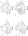
- FIGS. 7A-D are simplified perspective views of example planar, FinFET, gate-all-around, and stacked gate-all-around transistors. In some embodiments, these transistors may be implemented with asymmetric source and drain contacts (e.g., similar to transistor 100).
- the transistors illustrated in FIGS. 7A-7D are formed on a substrate 716 having a surface 708. Isolation regions 714 separate the source and drain regions of the transistors from other transistors and from a bulk region 718 of the substrate 716.
- FIG. 7A is a perspective view of an example planar transistor 700 comprising a gate 702 that controls current flow between a source region 704 and a drain region 706.
- the transistor 700 is planar in that the source region 704 and the drain region 706 are planar with respect to the substrate surface 708.
- FIG. 7B is a perspective view of an example FinFET transistor 720 comprising a gate 722 that controls current flow between a source region 724 and a drain region 726.
- the transistor 720 is non-planar in that the source region 724 and the drain region 726 comprise "fins" that extend upwards from the substrate surface 728.
- the transistor 720 can be considered a tri-gate transistor.
- FIG. 7B illustrates one S/D fin extending through the gate 722, but multiple S/D fins can extend through the gate of a FinFET transistor.
- FIG. 7C is a perspective view of a gate-all-around (GAA) transistor 740 comprising a gate 742 that controls current flow between a source region 744 and a drain region 746.
- the transistor 740 is non-planar in that the source region 744 and the drain region 746 are elevated from the substrate surface 728.
- FIG. 7D is a perspective view of a GAA transistor 760 comprising a gate 762 that controls current flow between multiple elevated source regions 764 and multiple elevated drain regions 766.
- the transistor 760 is a stacked GAA transistor as the gate controls the flow of current between multiple elevated S/D regions stacked on top of each other.
- the transistors 740 and 760 are considered gate-all-around transistors as the gates encompass all sides of the semiconductor portions that extends from the source regions to the drain regions.
- the transistors 740 and 760 can alternatively be referred to as nanowire, nanosheet, or nanoribbon transistors depending on the width (e.g., widths 748 and 768 of transistors 740 and 760, respectively) of the semiconductor portions extending through the gate.
- a transistor 640 may include a gate 622 formed of at least two layers, a gate dielectric and a gate electrode.
- the gate dielectric may include one layer or a stack of layers.
- the one or more layers may include silicon oxide, silicon dioxide, silicon carbide, and/or a high-k dielectric material.
- the high-k dielectric material may include elements such as hafnium, silicon, oxygen, titanium, tantalum, lanthanum, aluminum, zirconium, barium, strontium, yttrium, lead, scandium, niobium, and zinc.
- high-k materials that may be used in the gate dielectric include, but are not limited to, hafnium oxide, hafnium silicon oxide, lanthanum oxide, lanthanum aluminum oxide, zirconium oxide, zirconium silicon oxide, tantalum oxide, titanium oxide, barium strontium titanium oxide, barium titanium oxide, strontium titanium oxide, yttrium oxide, aluminum oxide, lead scandium tantalum oxide, and lead zinc niobate.
- an annealing process may be carried out on the gate dielectric to improve its quality when a high-k material is used.
- the gate electrode may be formed on the gate dielectric and may include at least one p-type work function metal or n-type work function metal, depending on whether the transistor 640 is to be a p-type metal oxide semiconductor (PMOS) or an n-type metal oxide semiconductor (NMOS) transistor.
- the gate electrode may consist of a stack of two or more metal layers, where one or more metal layers are work function metal layers and at least one metal layer is a fill metal layer. Further metal layers may be included for other purposes, such as a barrier layer.
- metals that may be used for the gate electrode include, but are not limited to, ruthenium, palladium, platinum, cobalt, nickel, conductive metal oxides (e.g., ruthenium oxide), and any of the metals discussed below with reference to an NMOS transistor (e.g., for work function tuning).
- metals that may be used for the gate electrode include, but are not limited to, hafnium, zirconium, titanium, tantalum, aluminum, alloys of these metals, carbides of these metals (e.g., hafnium carbide, zirconium carbide, titanium carbide, tantalum carbide, and aluminum carbide), and any of the metals discussed above with reference to a PMOS transistor (e.g., for work function tuning).
- the interconnect structures 628 may be arranged within the interconnect layers 606-610 to route electrical signals according to a wide variety of designs; in particular, the arrangement is not limited to the particular configuration of interconnect structures 628 depicted in FIG. 6 . Although a particular number of interconnect layers 606-610 is depicted in FIG. 6 , embodiments of the present disclosure include integrated circuit devices having more or fewer interconnect layers than depicted.
- the second interconnect layer 608 (referred to as Metal 2 or "M2") may be formed directly on the first interconnect layer 606.
- the second interconnect layer 608 may include via 628b to couple the lines 628 of the second interconnect layer 608 with the lines 628a of a third interconnect layer 610.
- the lines 628a and the vias 628b are structurally delineated with a line within individual interconnect layers for the sake of clarity, the lines 628a and the vias 628b may be structurally and/or materially contiguous (e.g., simultaneously filled during a dual-damascene process) in some embodiments.
- the third interconnect layer 610 (referred to as Metal 3 or "M3") (and additional interconnect layers, as desired) may be formed in succession on the second interconnect layer 608 according to similar techniques and configurations described in connection with the second interconnect layer 608 or the first interconnect layer 606.
- the interconnect layers that are "higher up” in the metallization stack 619 in the integrated circuit device 600 i.e., farther away from the device layer 604 may be thicker that the interconnect layers that are lower in the metallization stack 619, with lines 628a and vias 628b in the higher interconnect layers being thicker than those in the lower interconnect layers.
- the integrated circuit device 600 may include a solder resist material 634 (e.g., polyimide or similar material) and one or more conductive contacts 636 formed on the interconnect layers 606-610.
- the conductive contacts 636 are illustrated as taking the form of bond pads.
- the conductive contacts 636 may be electrically coupled with the interconnect structures 628 and configured to route the electrical signals of the transistor(s) 640 to external devices.
- solder bonds may be formed on the one or more conductive contacts 636 to mechanically and/or electrically couple an integrated circuit die including the integrated circuit device 600 with another component (e.g., a printed circuit board).
- the integrated circuit device 600 may include additional or alternate structures to route the electrical signals from the interconnect layers 606-610; for example, the conductive contacts 636 may include other analogous features (e.g., posts) that route the electrical signals to external components.
- the conductive contacts 636 may serve as any of the conductive contacts described throughout this disclosure.
- the integrated circuit device 600 may include another metallization stack (not shown) on the opposite side of the device layer(s) 604.
- This metallization stack may include multiple interconnect layers as discussed above with reference to the interconnect layers 606-610, to provide conductive pathways (e.g., including conductive lines and vias) between the device layer(s) 604 and additional conductive contacts (not shown) on the opposite side of the integrated circuit device 600 from the conductive contacts 636.
- conductive pathways e.g., including conductive lines and vias
- additional conductive contacts may serve as any of the conductive contacts described throughout this disclosure.
- the integrated circuit device 600 may include one or more through silicon vias (TSVs) through the die substrate 602; these TSVs may make contact with the device layer(s) 604, and may provide conductive pathways between the device layer(s) 604 and additional conductive contacts (not shown) on the opposite side of the integrated circuit device 600 from the conductive contacts 636. These additional conductive contacts may serve as any of the conductive contacts described throughout this disclosure.
- TSVs through silicon vias
- TSVs extending through the substrate can be used for routing power and ground signals from conductive contacts on the opposite side of the integrated circuit device 600 from the conductive contacts 636 to the transistors 640 and any other components integrated into the die 600, and the metallization stack 619 can be used to route I/O signals from the conductive contacts 636 to transistors 640 and any other components integrated into the die 600.
- the coupling components 816 may electrically and mechanically couple the package-on-interposer structure 836 to the circuit board 802, and may include solder balls (as shown in FIG. 8 ), pins (e.g., as part of a pin grid array (PGA), contacts (e.g., as part of a land grid array (LGA)), male and female portions of a socket, an adhesive, an underfill material, and/or any other suitable electrical and/or mechanical coupling structure.
- the coupling components 816 may serve as the coupling components illustrated or described for any of the substrate assembly or substrate assembly components described herein, as appropriate.
- the package-on-interposer structure 836 may include an integrated circuit component 820 coupled to an interposer 804 by coupling components 818.
- the coupling components 818 may take any suitable form for the application, such as the forms discussed above with reference to the coupling components 816. Although a single integrated circuit component 820 is shown in FIG. 8 , multiple integrated circuit components may be coupled to the interposer 804; indeed, additional interposers may be coupled to the interposer 804.
- the interposer 804 may provide an intervening substrate used to bridge the circuit board 802 and the integrated circuit component 820.
- the integrated circuit component 820 may be a packaged or unpackaged integrated circuit product that includes one or more integrated circuit dies (e.g., the die 502 of FIG. 5 , the integrated circuit device 600 of FIG. 6 ) and/or one or more other suitable components.
- a packaged integrated circuit component comprises one or more integrated circuit dies mounted on a package substrate with the integrated circuit dies and package substrate encapsulated in a casing material, such as a metal, plastic, glass, or ceramic.
- a single monolithic integrated circuit die comprises solder bumps attached to contacts on the die. The solder bumps allow the die to be directly attached to the interposer 804.
- the integrated circuit component 820 can comprise one or more computing system components, such as one or more processor units (e.g., system-on-a-chip (SoC), processor core, graphics processor unit (GPU), accelerator, chipset processor), I/O controller, memory, or network interface controller.
- processor units e.g., system-on-a-chip (SoC)
- SoC system-on-a-chip
- GPU graphics processor unit
- accelerator chipset processor
- I/O controller I/O controller
- memory or network interface controller.
- the integrated circuit component 820 can comprise one or more additional active or passive devices such as capacitors, decoupling capacitors, resistors, inductors, fuses, diodes, transformers, sensors, electrostatic discharge (ESD) devices, and memory devices.
- ESD electrostatic discharge
- the integrated circuit component 820 comprises multiple integrated circuit dies
- they dies can be of the same type (a homogeneous multi-die integrated circuit component) or of two or more different types (a heterogeneous multi-die integrated circuit component).
- a multi-die integrated circuit component can be referred to as a multi-chip package (MCP) or multi-chip module (MCM).
- the integrated circuit component 820 can comprise additional components, such as embedded DRAM, stacked high bandwidth memory (HBM), shared cache memories, input/output (I/O) controllers, or memory controllers. Any of these additional components can be located on the same integrated circuit die as a processor unit, or on one or more integrated circuit dies separate from the integrated circuit dies comprising the processor units. These separate integrated circuit dies can be referred to as "chiplets". In embodiments where an integrated circuit component comprises multiple integrated circuit dies, interconnections between dies can be provided by the package substrate, one or more silicon interposers, one or more silicon bridges embedded in the package substrate (such as Intel ® embedded multi-die interconnect bridges (EMIBs)), or combinations thereof.
- EMIBs Intel ® embedded multi-die interconnect bridges
- the interposer 804 may spread connections to a wider pitch or reroute a connection to a different connection.
- the interposer 804 may couple the integrated circuit component 820 to a set of ball grid array (BGA) conductive contacts of the coupling components 816 for coupling to the circuit board 802.
- BGA ball grid array
- the integrated circuit component 820 and the circuit board 802 are attached to opposing sides of the interposer 804; in other embodiments, the integrated circuit component 820 and the circuit board 802 may be attached to a same side of the interposer 804.
- three or more components may be interconnected by way of the interposer 804.
- the interposer 804 may be formed as a PCB, including multiple metal layers separated from one another by layers of dielectric material and interconnected by electrically conductive vias.
- the interposer 804 may be formed of an epoxy resin, a fiberglass-reinforced epoxy resin, an epoxy resin with inorganic fillers, a ceramic material, or a polymer material such as polyimide.
- the interposer 804 may be formed of alternate rigid or flexible materials that may include the same materials described above for use in a semiconductor substrate, such as silicon, germanium, and other group III-V and group IV materials.
- the interposer 804 may include metal interconnects 808 and vias 810, including but not limited to through hole vias 810-1 (that extend from a first face 850 of the interposer 804 to a second face 854 of the interposer 804), blind vias 810-2 (that extend from the first or second faces 850 or 854 of the interposer 804 to an internal metal layer), and buried vias 810-3 (that connect internal metal layers).
- through hole vias 810-1 that extend from a first face 850 of the interposer 804 to a second face 854 of the interposer 804
- blind vias 810-2 that extend from the first or second faces 850 or 854 of the interposer 804 to an internal metal layer
- buried vias 810-3 that connect internal metal layers.
- the interposer 804 can comprise a silicon interposer. Through silicon vias (TSV) extending through the silicon interposer can connect connections on a first face of a silicon interposer to an opposing second face of the silicon interposer.
- TSV through silicon vias
- an interposer 804 comprising a silicon interposer can further comprise one or more routing layers to route connections on a first face of the interposer 804 to an opposing second face of the interposer 804.
- the interposer 804 may further include embedded devices 814, including both passive and active devices. Such devices may include, but are not limited to, capacitors, decoupling capacitors, resistors, inductors, fuses, diodes, transformers, sensors, electrostatic discharge (ESD) devices, and memory devices. More complex devices such as radio frequency devices, power amplifiers, power management devices, antennas, arrays, sensors, and microelectromechanical systems (MEMS) devices may also be formed on the interposer 804.
- the package-on-interposer structure 836 may take the form of any of the package-on-interposer structures known in the art. In embodiments where the interposer is a non-printed circuit board
- the integrated circuit device assembly 800 may include an integrated circuit component 824 coupled to the first face 840 of the circuit board 802 by coupling components 822.
- the coupling components 822 may take the form of any of the embodiments discussed above with reference to the coupling components 816, and the integrated circuit component 824 may take the form of any of the embodiments discussed above with reference to the integrated circuit component 820.
- the integrated circuit device assembly 800 illustrated in FIG. 8 includes a package-on-package structure 834 coupled to the second face 842 of the circuit board 802 by coupling components 828.
- the package-on-package structure 834 may include an integrated circuit component 826 and an integrated circuit component 832 coupled together by coupling components 830 such that the integrated circuit component 826 is disposed between the circuit board 802 and the integrated circuit component 832.
- the coupling components 828 and 830 may take the form of any of the embodiments of the coupling components 816 discussed above, and the integrated circuit components 826 and 832 may take the form of any of the embodiments of the integrated circuit component 820 discussed above.
- the package-on-package structure 834 may be configured in accordance with any of the package-on-package structures known in the art.
- Example 16 includes the electronic device of any of Examples 12-15, wherein: the source contact is the wider contact and the drain contact is the narrower contact; or the drain contact is the wider contact and the source contact is the narrower contact.
- Example 18 includes a method, comprising: receiving a substrate; forming a channel over the substrate; forming a source and a drain over the substrate, wherein the source and the drain are coupled via the channel; forming a gate over the substrate, wherein the gate is coupled to the channel; and forming a source contact and a drain contact, wherein the source contact is coupled to the source and the drain contact is coupled to the drain, and wherein the source contact and the drain contact are asymmetric.
Landscapes
- Insulated Gate Type Field-Effect Transistor (AREA)
- Electrodes Of Semiconductors (AREA)
Applications Claiming Priority (1)
| Application Number | Priority Date | Filing Date | Title |
|---|---|---|---|
| US18/400,193 US20250220950A1 (en) | 2023-12-29 | 2023-12-29 | Transistors with asymmetric source and drain contacts |
Publications (1)
| Publication Number | Publication Date |
|---|---|
| EP4580336A1 true EP4580336A1 (de) | 2025-07-02 |
Family
ID=93924345
Family Applications (1)
| Application Number | Title | Priority Date | Filing Date |
|---|---|---|---|
| EP24220194.5A Pending EP4580336A1 (de) | 2023-12-29 | 2024-12-16 | Gaa-feldeffekttransistoren mit asymmetrischen rückseitigen source- und oberseitigen drain-kontakten |
Country Status (2)
| Country | Link |
|---|---|
| US (1) | US20250220950A1 (de) |
| EP (1) | EP4580336A1 (de) |
Citations (5)
| Publication number | Priority date | Publication date | Assignee | Title |
|---|---|---|---|---|
| US20220157956A1 (en) * | 2020-11-13 | 2022-05-19 | Taiwan Semiconductor Manufacturing Co., Ltd. | Forming a cavity with a wet etch for backside contact formation |
| US20230060786A1 (en) * | 2021-08-27 | 2023-03-02 | Taiwan Semiconductor Manufacturing Company, Ltd. | Enlarged Backside Contact |
| US11791387B2 (en) * | 2021-04-30 | 2023-10-17 | Taiwan Semiconductor Manufacturing Company, Ltd. | Semiconductor devices with backside via and methods thereof |
| EP4270484A2 (de) * | 2022-03-11 | 2023-11-01 | INTEL Corporation | Integrierte schaltungsstrukturen mit selbstjustiertem rückseitenkontakt zwischen einer leitfähigen quelle und einem drain |
| US20230386915A1 (en) * | 2022-05-26 | 2023-11-30 | Taiwan Semiconductor Manufacturing Company, Ltd. | Method for forming a contact plug by bottom-up metal growth |
-
2023
- 2023-12-29 US US18/400,193 patent/US20250220950A1/en active Pending
-
2024
- 2024-12-16 EP EP24220194.5A patent/EP4580336A1/de active Pending
Patent Citations (5)
| Publication number | Priority date | Publication date | Assignee | Title |
|---|---|---|---|---|
| US20220157956A1 (en) * | 2020-11-13 | 2022-05-19 | Taiwan Semiconductor Manufacturing Co., Ltd. | Forming a cavity with a wet etch for backside contact formation |
| US11791387B2 (en) * | 2021-04-30 | 2023-10-17 | Taiwan Semiconductor Manufacturing Company, Ltd. | Semiconductor devices with backside via and methods thereof |
| US20230060786A1 (en) * | 2021-08-27 | 2023-03-02 | Taiwan Semiconductor Manufacturing Company, Ltd. | Enlarged Backside Contact |
| EP4270484A2 (de) * | 2022-03-11 | 2023-11-01 | INTEL Corporation | Integrierte schaltungsstrukturen mit selbstjustiertem rückseitenkontakt zwischen einer leitfähigen quelle und einem drain |
| US20230386915A1 (en) * | 2022-05-26 | 2023-11-30 | Taiwan Semiconductor Manufacturing Company, Ltd. | Method for forming a contact plug by bottom-up metal growth |
Also Published As
| Publication number | Publication date |
|---|---|
| US20250220950A1 (en) | 2025-07-03 |
Similar Documents
| Publication | Publication Date | Title |
|---|---|---|
| WO2022132267A1 (en) | Microelectronic structures including glass cores | |
| US12288750B2 (en) | Conformal power delivery structure for direct chip attach architectures | |
| US20230411390A1 (en) | Two-dimensional pmos devices for providing cmos in back-end layers of integrated circuit devices | |
| US12242290B2 (en) | Integrating voltage regulators and passive circuit elements with top side power planes in stacked die architectures | |
| US20250112153A1 (en) | Virtual ground net for process-induced damage prevention | |
| WO2025071719A1 (en) | Die-to-die input/output signal routing utilizing opposing die surfaces in integrated circuit component packaging | |
| US20250112168A1 (en) | Hybrid bonding with embedded alignment markers | |
| US20230095654A1 (en) | Conformal power delivery structures | |
| US20240079335A1 (en) | Three-dimensional integration of dies in an integrated circuit device | |
| US20230395467A1 (en) | Glass core architectures with dielectric buffer layer between glass core and metal vias and pads | |
| US20230299123A1 (en) | Inductors for hybrid bonding interconnect architectures | |
| US20240006494A1 (en) | Source and drain refractory metal cap | |
| US20240222258A1 (en) | Glass substrates with self-assembled monolayers for copper adhesion | |
| EP4580336A1 (de) | Gaa-feldeffekttransistoren mit asymmetrischen rückseitigen source- und oberseitigen drain-kontakten | |
| US20230207421A1 (en) | Technologies for thermoelectric-enhanced cooling | |
| US20250385166A1 (en) | Frontside feedthrough connections | |
| US20250112122A1 (en) | Backside power gating | |
| EP4719026A2 (de) | Selbstausgerichtete rückseiten-durchkontaktierungen mit endpunkt-unterfinätzung | |
| US20260068174A1 (en) | Overhang architectures for high bandwidth memory (hbm) multi-die assemblies and methods for making same | |
| US20250210491A1 (en) | Vertically embedded utility patch for semiconductor packages | |
| EP4716410A1 (de) | Integrierte gate-all-around (gaa)/finfet-transistorvorrichtungen | |
| EP4468336A1 (de) | Wärmeableitungslösungen für integrierte schaltungspackungen | |
| US20240006488A1 (en) | Capping source and drain regions of transistors to prevent diffusion of dopants during fabrication | |
| US20240114693A1 (en) | Self-aligned patterning of plate lines in three-dimensional ferroelectric capacitors | |
| US20250218942A1 (en) | Via aligned with adjacent interconnect layers |
Legal Events
| Date | Code | Title | Description |
|---|---|---|---|
| PUAI | Public reference made under article 153(3) epc to a published international application that has entered the european phase |
Free format text: ORIGINAL CODE: 0009012 |
|
| STAA | Information on the status of an ep patent application or granted ep patent |
Free format text: STATUS: THE APPLICATION HAS BEEN PUBLISHED |
|
| AK | Designated contracting states |
Kind code of ref document: A1 Designated state(s): AL AT BE BG CH CY CZ DE DK EE ES FI FR GB GR HR HU IE IS IT LI LT LU LV MC ME MK MT NL NO PL PT RO RS SE SI SK SM TR |
|
| STAA | Information on the status of an ep patent application or granted ep patent |
Free format text: STATUS: REQUEST FOR EXAMINATION WAS MADE |
|
| 17P | Request for examination filed |
Effective date: 20260102 |