EP4580334A1 - Isolationswände mit luftspalt - Google Patents
Isolationswände mit luftspalt Download PDFInfo
- Publication number
- EP4580334A1 EP4580334A1 EP24215516.6A EP24215516A EP4580334A1 EP 4580334 A1 EP4580334 A1 EP 4580334A1 EP 24215516 A EP24215516 A EP 24215516A EP 4580334 A1 EP4580334 A1 EP 4580334A1
- Authority
- EP
- European Patent Office
- Prior art keywords
- transistor
- gate
- layer
- dielectric
- transistors
- Prior art date
- Legal status (The legal status is an assumption and is not a legal conclusion. Google has not performed a legal analysis and makes no representation as to the accuracy of the status listed.)
- Pending
Links
Images






Classifications
-
- H—ELECTRICITY
- H10—SEMICONDUCTOR DEVICES; ELECTRIC SOLID-STATE DEVICES NOT OTHERWISE PROVIDED FOR
- H10W—GENERIC PACKAGES, INTERCONNECTIONS, CONNECTORS OR OTHER CONSTRUCTIONAL DETAILS OF DEVICES COVERED BY CLASS H10
- H10W20/00—Interconnections in chips, wafers or substrates
- H10W20/40—Interconnections external to wafers or substrates, e.g. back-end-of-line [BEOL] metallisations or vias connecting to gate electrodes
- H10W20/41—Interconnections external to wafers or substrates, e.g. back-end-of-line [BEOL] metallisations or vias connecting to gate electrodes characterised by their conductive parts
- H10W20/427—Power or ground buses
-
- H—ELECTRICITY
- H10—SEMICONDUCTOR DEVICES; ELECTRIC SOLID-STATE DEVICES NOT OTHERWISE PROVIDED FOR
- H10D—INORGANIC ELECTRIC SEMICONDUCTOR DEVICES
- H10D84/00—Integrated devices formed in or on semiconductor substrates that comprise only semiconducting layers, e.g. on Si wafers or on GaAs-on-Si wafers
- H10D84/01—Manufacture or treatment
- H10D84/0123—Integrating together multiple components covered by H10D12/00 or H10D30/00, e.g. integrating multiple IGBTs
- H10D84/0126—Integrating together multiple components covered by H10D12/00 or H10D30/00, e.g. integrating multiple IGBTs the components including insulated gates, e.g. IGFETs
- H10D84/0151—Manufacturing their isolation regions
- H10D84/0153—Manufacturing their isolation regions using gate cut processes
-
- H—ELECTRICITY
- H10—SEMICONDUCTOR DEVICES; ELECTRIC SOLID-STATE DEVICES NOT OTHERWISE PROVIDED FOR
- H10D—INORGANIC ELECTRIC SEMICONDUCTOR DEVICES
- H10D30/00—Field-effect transistors [FET]
- H10D30/01—Manufacture or treatment
- H10D30/019—Manufacture or treatment of FETs having stacked nanowire, nanosheet or nanoribbon channels
- H10D30/0198—Manufacture or treatment of FETs having stacked nanowire, nanosheet or nanoribbon channels forming source or drain electrodes wherein semiconductor bodies are replaced by dielectric layers and the source or drain electrodes extend through the dielectric layers
-
- H—ELECTRICITY
- H10—SEMICONDUCTOR DEVICES; ELECTRIC SOLID-STATE DEVICES NOT OTHERWISE PROVIDED FOR
- H10D—INORGANIC ELECTRIC SEMICONDUCTOR DEVICES
- H10D30/00—Field-effect transistors [FET]
- H10D30/40—FETs having zero-dimensional [0D], one-dimensional [1D] or two-dimensional [2D] charge carrier gas channels
- H10D30/43—FETs having zero-dimensional [0D], one-dimensional [1D] or two-dimensional [2D] charge carrier gas channels having one-dimensional [1D] charge carrier gas channels, e.g. quantum wire FETs or transistors having 1D quantum-confined channels
-
- H—ELECTRICITY
- H10—SEMICONDUCTOR DEVICES; ELECTRIC SOLID-STATE DEVICES NOT OTHERWISE PROVIDED FOR
- H10D—INORGANIC ELECTRIC SEMICONDUCTOR DEVICES
- H10D30/00—Field-effect transistors [FET]
- H10D30/60—Insulated-gate field-effect transistors [IGFET]
- H10D30/67—Thin-film transistors [TFT]
- H10D30/6729—Thin-film transistors [TFT] characterised by the electrodes
- H10D30/673—Thin-film transistors [TFT] characterised by the electrodes characterised by the shapes, relative sizes or dispositions of the gate electrodes
- H10D30/6735—Thin-film transistors [TFT] characterised by the electrodes characterised by the shapes, relative sizes or dispositions of the gate electrodes having gates fully surrounding the channels, e.g. gate-all-around
-
- H—ELECTRICITY
- H10—SEMICONDUCTOR DEVICES; ELECTRIC SOLID-STATE DEVICES NOT OTHERWISE PROVIDED FOR
- H10D—INORGANIC ELECTRIC SEMICONDUCTOR DEVICES
- H10D30/00—Field-effect transistors [FET]
- H10D30/60—Insulated-gate field-effect transistors [IGFET]
- H10D30/67—Thin-film transistors [TFT]
- H10D30/6757—Thin-film transistors [TFT] characterised by the structure of the channel, e.g. transverse or longitudinal shape or doping profile
-
- H—ELECTRICITY
- H10—SEMICONDUCTOR DEVICES; ELECTRIC SOLID-STATE DEVICES NOT OTHERWISE PROVIDED FOR
- H10D—INORGANIC ELECTRIC SEMICONDUCTOR DEVICES
- H10D62/00—Semiconductor bodies, or regions thereof, of devices having potential barriers
- H10D62/10—Shapes, relative sizes or dispositions of the regions of the semiconductor bodies; Shapes of the semiconductor bodies
- H10D62/117—Shapes of semiconductor bodies
- H10D62/118—Nanostructure semiconductor bodies
- H10D62/119—Nanowire, nanosheet or nanotube semiconductor bodies
- H10D62/121—Nanowire, nanosheet or nanotube semiconductor bodies oriented parallel to substrates
-
- H—ELECTRICITY
- H10—SEMICONDUCTOR DEVICES; ELECTRIC SOLID-STATE DEVICES NOT OTHERWISE PROVIDED FOR
- H10D—INORGANIC ELECTRIC SEMICONDUCTOR DEVICES
- H10D64/00—Electrodes of devices having potential barriers
- H10D64/20—Electrodes characterised by their shapes, relative sizes or dispositions
- H10D64/23—Electrodes carrying the current to be rectified, amplified, oscillated or switched, e.g. sources, drains, anodes or cathodes
- H10D64/251—Source or drain electrodes for field-effect devices
-
- H—ELECTRICITY
- H10—SEMICONDUCTOR DEVICES; ELECTRIC SOLID-STATE DEVICES NOT OTHERWISE PROVIDED FOR
- H10D—INORGANIC ELECTRIC SEMICONDUCTOR DEVICES
- H10D84/00—Integrated devices formed in or on semiconductor substrates that comprise only semiconducting layers, e.g. on Si wafers or on GaAs-on-Si wafers
- H10D84/01—Manufacture or treatment
- H10D84/0123—Integrating together multiple components covered by H10D12/00 or H10D30/00, e.g. integrating multiple IGBTs
- H10D84/0126—Integrating together multiple components covered by H10D12/00 or H10D30/00, e.g. integrating multiple IGBTs the components including insulated gates, e.g. IGFETs
- H10D84/0165—Integrating together multiple components covered by H10D12/00 or H10D30/00, e.g. integrating multiple IGBTs the components including insulated gates, e.g. IGFETs the components including complementary IGFETs, e.g. CMOS devices
- H10D84/0188—Manufacturing their isolation regions
-
- H—ELECTRICITY
- H10—SEMICONDUCTOR DEVICES; ELECTRIC SOLID-STATE DEVICES NOT OTHERWISE PROVIDED FOR
- H10D—INORGANIC ELECTRIC SEMICONDUCTOR DEVICES
- H10D84/00—Integrated devices formed in or on semiconductor substrates that comprise only semiconducting layers, e.g. on Si wafers or on GaAs-on-Si wafers
- H10D84/80—Integrated devices formed in or on semiconductor substrates that comprise only semiconducting layers, e.g. on Si wafers or on GaAs-on-Si wafers characterised by the integration of at least one component covered by groups H10D12/00 or H10D30/00, e.g. integration of IGFETs
- H10D84/82—Integrated devices formed in or on semiconductor substrates that comprise only semiconducting layers, e.g. on Si wafers or on GaAs-on-Si wafers characterised by the integration of at least one component covered by groups H10D12/00 or H10D30/00, e.g. integration of IGFETs of only field-effect components
- H10D84/83—Integrated devices formed in or on semiconductor substrates that comprise only semiconducting layers, e.g. on Si wafers or on GaAs-on-Si wafers characterised by the integration of at least one component covered by groups H10D12/00 or H10D30/00, e.g. integration of IGFETs of only field-effect components of only insulated-gate FETs [IGFET]
-
- H—ELECTRICITY
- H10—SEMICONDUCTOR DEVICES; ELECTRIC SOLID-STATE DEVICES NOT OTHERWISE PROVIDED FOR
- H10D—INORGANIC ELECTRIC SEMICONDUCTOR DEVICES
- H10D84/00—Integrated devices formed in or on semiconductor substrates that comprise only semiconducting layers, e.g. on Si wafers or on GaAs-on-Si wafers
- H10D84/80—Integrated devices formed in or on semiconductor substrates that comprise only semiconducting layers, e.g. on Si wafers or on GaAs-on-Si wafers characterised by the integration of at least one component covered by groups H10D12/00 or H10D30/00, e.g. integration of IGFETs
- H10D84/82—Integrated devices formed in or on semiconductor substrates that comprise only semiconducting layers, e.g. on Si wafers or on GaAs-on-Si wafers characterised by the integration of at least one component covered by groups H10D12/00 or H10D30/00, e.g. integration of IGFETs of only field-effect components
- H10D84/83—Integrated devices formed in or on semiconductor substrates that comprise only semiconducting layers, e.g. on Si wafers or on GaAs-on-Si wafers characterised by the integration of at least one component covered by groups H10D12/00 or H10D30/00, e.g. integration of IGFETs of only field-effect components of only insulated-gate FETs [IGFET]
- H10D84/85—Complementary IGFETs, e.g. CMOS
- H10D84/851—Complementary IGFETs, e.g. CMOS comprising IGFETs having stacked nanowire, nanosheet or nanoribbon channels
-
- H—ELECTRICITY
- H10—SEMICONDUCTOR DEVICES; ELECTRIC SOLID-STATE DEVICES NOT OTHERWISE PROVIDED FOR
- H10D—INORGANIC ELECTRIC SEMICONDUCTOR DEVICES
- H10D88/00—Three-dimensional [3D] integrated devices
-
- H—ELECTRICITY
- H10—SEMICONDUCTOR DEVICES; ELECTRIC SOLID-STATE DEVICES NOT OTHERWISE PROVIDED FOR
- H10D—INORGANIC ELECTRIC SEMICONDUCTOR DEVICES
- H10D88/00—Three-dimensional [3D] integrated devices
- H10D88/01—Manufacture or treatment
-
- H—ELECTRICITY
- H10—SEMICONDUCTOR DEVICES; ELECTRIC SOLID-STATE DEVICES NOT OTHERWISE PROVIDED FOR
- H10W—GENERIC PACKAGES, INTERCONNECTIONS, CONNECTORS OR OTHER CONSTRUCTIONAL DETAILS OF DEVICES COVERED BY CLASS H10
- H10W10/00—Isolation regions in semiconductor bodies between components of integrated devices
- H10W10/01—Manufacture or treatment
- H10W10/021—Manufacture or treatment of air gaps
-
- H—ELECTRICITY
- H10—SEMICONDUCTOR DEVICES; ELECTRIC SOLID-STATE DEVICES NOT OTHERWISE PROVIDED FOR
- H10W—GENERIC PACKAGES, INTERCONNECTIONS, CONNECTORS OR OTHER CONSTRUCTIONAL DETAILS OF DEVICES COVERED BY CLASS H10
- H10W10/00—Isolation regions in semiconductor bodies between components of integrated devices
- H10W10/20—Air gaps
-
- B—PERFORMING OPERATIONS; TRANSPORTING
- B82—NANOTECHNOLOGY
- B82Y—SPECIFIC USES OR APPLICATIONS OF NANOSTRUCTURES; MEASUREMENT OR ANALYSIS OF NANOSTRUCTURES; MANUFACTURE OR TREATMENT OF NANOSTRUCTURES
- B82Y10/00—Nanotechnology for information processing, storage or transmission, e.g. quantum computing or single electron logic
-
- H—ELECTRICITY
- H10—SEMICONDUCTOR DEVICES; ELECTRIC SOLID-STATE DEVICES NOT OTHERWISE PROVIDED FOR
- H10D—INORGANIC ELECTRIC SEMICONDUCTOR DEVICES
- H10D84/00—Integrated devices formed in or on semiconductor substrates that comprise only semiconducting layers, e.g. on Si wafers or on GaAs-on-Si wafers
- H10D84/01—Manufacture or treatment
- H10D84/02—Manufacture or treatment characterised by using material-based technologies
- H10D84/03—Manufacture or treatment characterised by using material-based technologies using Group IV technology, e.g. silicon technology or silicon-carbide [SiC] technology
- H10D84/038—Manufacture or treatment characterised by using material-based technologies using Group IV technology, e.g. silicon technology or silicon-carbide [SiC] technology using silicon technology, e.g. SiGe
Definitions
- Transistor-based IC devices have isolation materials between different conductive components.
- the isolation materials provide electrical isolation between different components of transistors, e.g., between a gate and a source region.
- the isolation materials also provide electrical isolation between different transistors, e.g., between the gates of adjacent transistors.
- a dielectric material is used as an isolation material between different conductive components in an IC device. Capacitance is proportional to the dielectric constant or relative permittivity of the material between two conductors, e.g., two adjacent gates, or a gate and a via next to the gate. Materials having a higher dielectric constant resulting in greater capacitance. Reducing the dielectric constant reduces the capacitance between conductors. Silicon dioxide is a common dielectric material that has a dielectric constant of 3.9. Dielectric materials with higher dielectric constants, such as silicon nitride, are often used between gates, as higher-k materials are often more robust than lower-k materials. Air gaps, with a dielectric constant of around 1, dramatically reduce capacitance relative to common dielectric materials.
- air gaps are incorporated into the device layer to reduce capacitance between conductive components of the IC device.
- a gate cut dielectric e.g., silicon nitride
- the air gap may extend between two adjacent gates (of two adjacent transistors), or between a gate and a via that extends through the gate line, between two gates.
- air gaps may extend between adjacent source or drain regions of pairs of adjacent transistors, e.g., in a device that includes back side source or drain contacts.
- the air gap may be formed from the back side of the transistor layer.
- a transistor layer may be formed over a support structure, followed by several layers of front side interconnect. The device may then be flipped and the support structure removed to expose the back side of the transistor layer. Material in the transistor layer is etched from the back side to create the air gaps. The air gaps are then capped by a dielectric material, so that additional layers (e.g., back side interconnect layers) may be formed over the air gap.
- a gate stack that may include one or more gate electrode materials and a gate dielectric may be provided around a portion of an elongated semiconductor structure called "nanoribbon", forming the gate stack on all sides of the nanoribbon.
- a source region and a drain region are provided on the opposite ends of the nanoribbon(s) and on either side of the gate stack, forming, respectively, a source and a drain of the nanoribbon transistor.
- the source and drain regions are insulated from the gate stack, so that the voltages at the three terminals (gate, source, and drain) may be separately controlled.
- Non-planar transistors provide several advantages over planar transistor architectures. For example, non-planar transistors provide improved electrostatic transistor control and faster transistor speeds relative to other transistor architectures. For certain applications, nanoribbon-based channels are particularly advantageous, providing increased drive current at smaller scales relative to other non-planar architectures.
- CMOS complementary metal-oxide-semiconductor
- N-channel FET may operate as an enhancement mode transistor
- P-channel FET may operate as a depletion mode transistor.
- CFETs may be employed in digital logic gates, memory cells, and various integrated circuits (ICs). The complementary nature of CFETs may reduce power consumption and/or enhance overall circuit performance in modern electronic devices.
- a layer of NMOS devices may be stacked over a layer of PMOS devices, or vice versa.
- the CFET transistors may have a non-planar transistor architecture, e.g., the transistors may be FinFETs, gate all-around transistors, nanoribbon transistors, nanowire transistors, or another transistor architecture.
- individual transistors may be aligned and stacked, e.g., an NMOS transistor in the NMOS layer may be stacked over a PMOS transistor in the PMOS layer.
- a pair of transistors (e.g., a stacked NMOS and PMOS transistor) may be coupled together in a circuit, e.g., connected in parallel or in series with each other.
- IC devices typically include a metallization stack, which is a collection of several metal layers, stacked above one another, in which different interconnects are provided.
- a metallization stack which is a collection of several metal layers, stacked above one another, in which different interconnects are provided.
- both front side interconnect layers and back side interconnect layers also referred to as front side metallization and back side metallization, are included.
- the front and back side metallization are provided on opposite sides of the transistor layer.
- Interconnect layers also referred to as metal layers, include electrically conductive trenches, also referred to as lines, which provide connectivity across the layer, and electrically conductive vias (or, simply, "vias”) that provide electrical connectivity between different layers.
- the term “trench” or “line” may be used to describe an electrically conductive element isolated by an insulator material (e.g., an insulator material typically comprising a low-k dielectric) that is provided in a plane parallel to the plane of an IC die/chip or a support structure over which an IC structure is provided, while the term “via” may be used to describe an electrically conductive element that interconnects two or more trenches of different levels of a metallization stack, or a component of the transistor layer and one or more trenches of a metallization layer.
- an insulator material e.g., an insulator material typically comprising a low-k dielectric
- a via may be provided substantially perpendicularly to the plane of an IC die/chip or a support structure over which an IC structure is provided, and the via may interconnect two trenches in adjacent levels, two trenches in not adjacent levels, and/or a component of a transistor layer and a trench in adjacent or not adjacent layers.
- trenches and vias may be referred to as "metal trenches/tracks/lines/traces” and “metal vias", respectively, to highlight the fact that these elements include electrically conductive materials such as, but not limited to, metals.
- trenches and vias may be referred to as "interconnects," where the term “interconnect” may be used to describe any element formed of an electrically conductive material for providing electrical connectivity to/from one or more components associated with an IC or/and between various such components.
- components associated with an IC include, for example, transistors, diodes, power sources, resistors, capacitors, inductors, sensors, transceivers, receivers, antennas, etc.
- Components associated with an IC may include those that are mounted on an IC or those connected to an IC.
- the IC may be either analog or digital and may be used in a number of applications, such as microprocessors, optoelectronics, logic blocks, audio amplifiers, etc., depending on the components associated with the IC.
- the IC may be employed as part of a chipset for executing one or more related functions in a computer.
- the phrase “A and/or B” means (A), (B), or (A and B).
- the phrase “A, B, and/or C” means (A), (B), (C), (A and B), (A and C), (B and C), or (A, B, and C).
- the term “between,” when used with reference to measurement ranges, is inclusive of the ends of the measurement ranges.
- the meaning of “a,” “an,” and “the” include plural references.
- the meaning of "in” includes “in” and "on.”
- FIGS. 1A-1B For convenience, if a collection of drawings designated with different letters are present, e.g., FIGS. 1A-1B , such a collection may be referred to herein without the letters, e.g., as " FIG. 1 .”
- FIGs. 1A-1B illustrate an example architecture of a nanoribbon-based transistor.
- FIG. 1A is a cross-section across a transistor 100 showing the source, gate, and drain.
- FIG. 1B is a cross-section across the gate regions of the transistor 100.
- FIG. 1B is a cross-section through the plane AA' in FIG. 1A
- FIG. 1A is a cross-section through the plane BB' in FIG. 1B .
- implementations of the present disclosure may be formed or carried out on a support structure, e.g., the support structure 102 illustrated in FIG. 1 .
- the support structure 102 may be, e.g., a substrate, a die, a wafer or a chip.
- the support structure may be the wafer 1500 of FIG. 11A , discussed below, and may be, or be included in, a die, e.g., the singulated die 1502 of FIG. 11B , discussed below.
- the support structure 102 extends along the x-y plane in the coordinate system shown in FIG. 1 .
- a support structure 102 may be used during a fabrication process and later removed.
- a top side of the transistor 100 may be attached to a second support structure (e.g., a second one of the support structures 102, which may be referred to as a carrier structure), and the support structure 102 over which the transistor 100 is formed may be removed to expose the back side of the transistor 100.
- a second support structure e.g., a second one of the support structures 102, which may be referred to as a carrier structure
- the support structure may be a substrate that includes silicon and/or hafnium. More generally, the support structure may be a semiconductor substrate composed of semiconductor material systems including, for example, N-type or P-type materials systems. In one implementation, the semiconductor substrate may be a crystalline substrate formed using a bulk silicon or a silicon-on-insulator (SOI) substructure.
- SOI silicon-on-insulator
- the semiconductor substrate may be formed using alternate materials, which may or may not be combined with silicon, that include, but are not limited to, germanium, silicon germanium, indium antimonide, lead telluride, indium arsenide, indium phosphide, gallium arsenide, aluminum gallium arsenide, aluminum arsenide, indium aluminum arsenide, aluminum indium antimonide, indium gallium arsenide, gallium nitride, indium gallium nitride, aluminum indium nitride or gallium antimonide, or other combinations of group III-V materials (i.e., materials from groups III and V of the periodic system of elements), group II-VI (i.e., materials from groups II and IV of the periodic system of elements), or group IV materials (i.e., materials from group IV of the periodic system of elements).
- group III-V materials i.e., materials from groups III and V of the periodic system of elements
- group II-VI i.e., materials from groups II and
- the substrate may be non-crystalline.
- the support structure may be a printed circuit board (PCB) substrate.
- PCB printed circuit board
- a transistor 100 is formed over a support structure 102.
- the transistor 100 includes a channel material 104 formed into four nanoribbons stacked on top of each other.
- the transistor 100 may include more or fewer nanoribbons, e.g., one, two, three, five, six or more nanoribbons.
- the channel material 104 may be a semiconductor, such as silicon or other semiconductor materials described herein.
- the transistor 100 includes nanoribbons 120a, 120b, 120c, and 120d, referred to collectively as nanoribbons 120 or individually as a nanoribbon 120.
- Each nanoribbon 120 is at a different height in the z-direction in the orientation shown in FIGs. 1A and 1B , i.e., a different distance from the support structure 102, where the nanoribbon 120a is the greatest distance from the support structure 102, and the nanoribbon 120d is the smallest distance from the support structure 102.
- S/D regions 108a and 108b are formed at either end of the nanoribbon channels 120, as illustrated in FIG. 1A .
- the channel material 104 may include one or more of cobalt oxide, copper oxide, ruthenium oxide, nickel oxide, niobium oxide, copper peroxide, indium telluride, molybdenite, molybdenum diselenide, tungsten diselenide, tungsten disulfide, molybdenum disulfide, N- or P-type amorphous or polycrystalline silicon, monocrystalline silicon, germanium, indium arsenide, indium gallium arsenide, indium selenide, indium antimonide, zinc antimonide, antimony selenide, silicon germanium, gallium nitride, aluminum gallium nitride, indium phosphite, black phosphorus, zinc sulfide, indium sulfide, gallium sulfide, each of which may possibly be doped with one or more of gallium, indium, aluminum, fluorine, boron, phosphorus, arsenic, nitrogen, tantalum, tungsten
- the high-k dielectric may be formed over the oxide.
- the gate electrode 110 surrounds the gate dielectric 112, e.g., the high-k dielectric (if included). In this example, the gate electrode 110 is above and below the nanoribbon stack, and between adjacent nanoribbons 120.
- high-k materials examples include, but are not limited to, hafnium oxide, hafnium silicon oxide, lanthanum oxide, lanthanum aluminum oxide, zirconium oxide, zirconium silicon oxide, tantalum oxide, titanium oxide, barium strontium titanium oxide, barium titanium oxide, strontium titanium oxide, yttrium oxide, aluminum oxide, tantalum oxide, tantalum silicon oxide, lead scandium tantalum oxide, and lead zinc niobate.
- the gate dielectric 112 may have a thickness between about 0.5 nanometers and 3 nanometers, including all values and ranges therein, e.g., between about 1 and 3 nanometers, or between about 1 and 2 nanometers.
- a transistor layer with through-layer vias is provided.
- a transistor layer including nanoribbon transistors 100 may be fabricated using known fabrication processes.
- the transistor layer may be formed over a support structure, such as the support structure 102.
- a front side metallization stack may be built up over the transistor layer, i.e., over a "front side" or top of the transistor layer.
- the front side metallization stack may include electrical connections to S/D regions and gate electrodes.
- a carrier structure may be attached to the top or front of the front side metallization stack, and the assembly may be flipped, so that the support structure over which the transistor layer was formed is facing up.
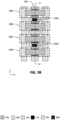
- FIGs. 3A and 3B provide cross-sections of a portion of a transistor layer over a front side metallization stack, according to some embodiments of the present disclosure.
- FIG. 3B is a cross-section through the plane CC' in FIG. 3A , illustrating the transistor layer and the front side metallization stack
- FIG. 3A is a cross-section through the plane DD' in FIG. 3B , illustrating a cross-section through the transistor layer.
- FIGs. 3A and 3B illustrate different cross-sections through four nanoribbon transistors 100a, 100b, 100c, and 100d.
- the nanoribbon transistors 100a-100d are examples of the nanoribbon transistor 100 described with respect to FIG. 1 .
- FIG. 3A illustrates the nanoribbon transistors 100 in a cross-section through the gate stack 116 in the y-z plane, which corresponds to the cross-section shown in FIG. 1B .
- the nanoribbon transistors 100 may be formed as described with respect to FIG. 1 .
- the nanoribbon transistors 100 are in a transistor layer 320, which may also be referred to as a device layer 320.
- an oxide material 312 is directly over the nanoribbon transistors 100.
- the oxide material 312 forms oxide regions 332, e.g., the oxide region 332a over the transistor 100a, and the oxide region 332b over the transistor 100b.
- the oxide material 312 may be a dielectric material that includes oxygen.
- the oxide regions 332 may be formed prior to forming the nanoribbon transistors 100 or at a later time, e.g., after the back side of the transistor layer 320 is exposed.
- FIG. 3B illustrates a gate line 350 that extends through the gate electrodes 110, gate dielectric 112, and the gate cut dielectric 302.
- FIG. 3B also illustrates the two S/D regions 108 on either side of the gate line 350.
- the channel material 104 of the nanoribbons extends through the gate electrode 110 and gate dielectric 112, and the channel material 104 extends between the S/D regions 108.
- one or more other dielectric materials e.g., the dielectric material 106) may fill other areas of the transistor layer 320 outside of the gate cut dielectric 302.
- the gate cut dielectric 302 may be included outside of the gate area, e.g., the gate cut dielectric 302 can extend into or through areas around the S/D regions 108.
- the gate cut dielectric 302 is a high-k dielectric. In certain embodiments, the gate cut dielectric 302 includes nitrogen. The gate cut dielectric 302 may include silicon and nitrogen, e.g., silicon nitride. In other embodiments, the gate cut dielectric 302 may include one or more dielectric materials that may include, but are not limited to, elements such as hafnium, silicon, oxygen, nitrogen, titanium, tantalum, lanthanum, aluminum, zirconium, barium, strontium, yttrium, lead, scandium, niobium, and zinc.
- elements such as hafnium, silicon, oxygen, nitrogen, titanium, tantalum, lanthanum, aluminum, zirconium, barium, strontium, yttrium, lead, scandium, niobium, and zinc.
- dielectric materials include, but are not limited to silicon oxide, silicon dioxide, silicon carbide, silicon nitride doped with carbon, silicon oxynitride, hafnium oxide, hafnium silicon oxide, lanthanum oxide, lanthanum aluminum oxide, zirconium oxide, zirconium silicon oxide, tantalum oxide, titanium oxide, barium strontium titanium oxide, barium titanium oxide, strontium titanium oxide, yttrium oxide, aluminum oxide, tantalum oxide, tantalum silicon oxide, lead scandium tantalum oxide, and lead zinc niobate.
- the transistor layer 320 is over (i.e., on top of) a front side metallization stack 322.
- the metallization stack 322 is over a support structure 102.
- the support structure 102 may be a carrier wafer that is coupled to the front side metallization stack 322 by a bonding layer 310.
- the carrier wafer may be bonded to the front side metallization stack 322 after fabrication of the front side metallization stack 322.
- the assembly i.e., the transistor layer 320, front side metallization stack 322, bonding layer 310, and carrier wafer
- the assembly may be flipped after bonding the carrier wafer, and a support structure over which the transistor layer 320 was formed may be removed, e.g., by grinding or polishing.
- the front side metallization stack 322 includes three front side metal layers 324a, 324b, and 324c, also referred to as interconnect layers.
- the metal layer 324a is the nearest metal layer to the transistor layer 320
- the metal layer 324c is the farthest metal layer from the transistor layer 320. While three metal layers 324a, 324b, and 324c are illustrated in FIG. 3A , an IC device may have fewer or more front side metal layers, e.g., up to 10 metal layers, up to 15 metal layers, or more.
- Each metal layer 324 includes conductive structures, including metal lines or trenches (e.g., the line 326) formed from a conductive material 308 and vias (e.g., the via 328) formed from the conductive material 308.
- the conductive material 308 may include one or more metals or metal alloys, with materials such as copper, ruthenium, palladium, platinum, cobalt, nickel, hafnium, zirconium, titanium, tantalum, and aluminum, tantalum nitride, tungsten, doped silicon, doped germanium, or alloys and mixtures of any of these.
- the conductive material 308 may include one or more electrically conductive alloys, oxides, or carbides of one or more metals. While FIG.
- any suitable conductive material may be used.
- the same conductive material may be used for both metal lines and vias, or different materials may be used for metal lines and vias.
- different materials may be used for the metal lines and/or vias, e.g., ruthenium may be included in the metal lines in the metal layer 324a, while copper is included in the metal lines in the metal layer 324c.
- conductive structures may include multiple conductive materials, e.g., a first metal as a liner, and a second metal as a fill.
- the conductive material 308 may form conductive pathways to route power, ground, and/or signals to/from various components of the transistor layer 320.
- the arrangement of the conductive material 308 in the front side metallization stack 322 in FIG. 3A is merely illustrative, and the conductive pathways in the front side metallization stack 322 may be connected to one another in any suitable manner.
- the metal lines and vias in the in the front side metallization stack 322 are surrounded by a dielectric material 306.
- the dielectric material 306 may be a low-k dielectric.
- the dielectric material 306 may include any of the materials described above with respect to the gate cut dielectric 302.
- different dielectric materials may be included in different ones of the metal layers, e.g., the metal layer 324a may include a different dielectric material from the metal layer 324c.
- multiple dielectric materials may be present in a given layer.
- the assembly shown in FIG. 3A and 3B further includes vias 330a and 330b (referred to jointly as vias 330) between certain pairs of adjacent gates.
- the vias 330 are formed within the gate cut regions and between adjacent gates.
- the vias 330 may be used for power and/or signal delivery between the back and front sides of the transistor layer 320, e.g., between the front side metallization stack 322 and a back side metallization stack formed later in the process.
- the via 330a is between the gates of the transistors 100a and 100b, and the via 330b is between the gates of the transistors 100c and 100d.
- the gate cut dielectric 302 fills the area between the gates of the transistors 100b and 100c.
- the vias 330 include a via material 304.
- the via material 304 may be a conductive material, such as a metal. Any of the conductive materials 308 described above may be used as or included in the via material 304.
- the vias 330a and 330b are in the transistor layer 320, and, in the orientation shown, the vias 330 extend above the transistor layer 320.
- the vias 330 extend downward to the front side metallization stack 322.
- the via 330b is over the via 328, and the via 330b is in electrical and physical contact with the via 328.
- a portion of the gate cut dielectric 302 is patterned and etched, and the via material 304 is deposited in the etched regions.
- a process to remove at least some of the gate cut dielectric is performed.
- the gate cut dielectric is etched from the exposed back side of the assembly, e.g., from the top of the assembly in the orientation of FIG. 3A .
- the etch chemistry may be highly selective to the gate cut dielectric 302 (e.g., silicon and/or nitrogen) so that other structures within the assembly are not removed or damaged by the etching process. For example, the oxide regions over the gate electrodes are left substantially intact.
- Removal of the gate cut dielectric forms air gaps within the transistor layer. The air gaps are created between adjacent gates and/or next to vias within the transistor layer, e.g., between a via and a gate.
- the gate cut dielectric may be patterned, e.g., using a lithographic process, so that portions of the gate cut dielectric are removed while others are not.
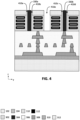
- FIG. 4 is a cross-section illustrating etching of portions of the gate cut dielectric, according to some embodiments of the present disclosure.
- the gate cut dielectric 402 is removed between the gate electrodes 110 of the four illustrated transistors, resulting in air gaps 410a and 410b on either side of the via 330a, air gaps 410c and 410d on either side of the via 330b, and the air gap 410e between the gates of the transistors 100b and 100c.
- a process to deposit a dielectric over the air gaps is performed.
- the dielectric may form caps over the air gaps formed in the process 204.
- the dielectric material is deposited such that the dielectric material covers, but does not fill, the air gaps.
- the dielectric material may be deposited some distance into the air gaps, but at least a portion of each air gap remains after the dielectric deposition.
- PVD physical vapor deposition
- CVD chemical vapor deposition
- the ends of the vias are exposed, e.g., by polishing the dielectric material deposited over the oxide regions 332, air gaps 410, and vias 330.
- the dielectric material that filled the top portion of the air gaps remains, capping the air gaps 410.
- FIG. 6 is a cross-section illustrating exposure, or reveal, of the vias 330 that extend through the transistor layer 320, according to some embodiments of the present disclosure.
- the portion of the dielectric material 502 that extended over the oxide regions 332 and the vias 330 has been removed, exposing the upper surfaces of the vias 330a and 330b and the upper surfaces of the oxide regions 332.
- the portions of the dielectric material 502 within the air gaps 410 remains, forming caps 612 over the air gaps 610.
- the resulting air gaps 610 after formation of the caps 612 have smaller volumes than the air gaps 410, as upper portions of the air gaps 410 have been replaced with the dielectric material 502.
- the cap 612a is over the air gap 610a
- the cap 612b is over the air gap 610b
- the cap 612c is over the air gap 610c
- the cap 612d is over the air gap 610d
- the cap 612e is over the air gap 610e.
- the cap 612a is bounded on the left side by the oxide region 332a and on the right side by the via 330a.
- the cap 612b is bounded on the left side by the via 330a and on the right side by the oxide region 332b.
- the cap 612e is bounded on either side by the oxide regions 332b and 332c.
- back side metallization is formed over the back side of the transistor layer, and over the capped air gaps.
- the back side metallization may be formed in a similar manner to the front side metallization.
- the back side metallization may include electrical connections to at least a portion of the vias that extend through the transistor layer.
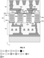
- Each back side metal layer 724 includes conductive structures, including metal lines or trenches formed from a conductive material 308 and vias formed from the conductive material 308. While FIG. 7A illustrates the same conductive material 308 for the vias and the metal lines within the back side metallization stack 722 that were included in the front side metallization stack 322, any suitable conductive material may be used, as described with respect to the front side metallization stack 322. Similarly, while the metal lines and vias in the in the back side metallization stack 722 are surrounded by the dielectric material 306, any suitable dielectric material or combination of dielectric materials may be used.
- the conductive material 308 may form conductive pathways to route power, ground, and/or signals to/from various components of the transistor layer 320.
- the arrangement of the conductive material 308 in the back side metallization stack 722 in FIG. 7A is merely illustrative, and the conductive pathways in the back side metallization stack 722 may be connected to one another in any suitable manner.
- the via 330b that extends through the transistor layer 320 is coupled to the via 726 in the back side metallization stack 722.
- This connection may provide power delivery from the back side of the IC device, through the back side metallization stack 722, into the via 726, through the via 330b, and to the front side metallization stack 322 by way of the via 328.
- a portion of the via 726 is over the cap 612d; the cap 612d prevents the conductive material 308 from the via 726 from entering the air gap 610d.
- FIG. 7B is an enlarged view of a portion 700 of FIG. 7A .
- FIG. 7B more clearly shows a pair of air gaps 610a and 610b around the via 330a.
- the air gap 610a is between the gate electrode 110a of the transistor 100a and the via 330a
- the air gap 610b is between the gate electrode 110b of the transistor 100b and the via 330a.
- the air gaps 610 provide isolation walls between conductive components, e.g., the via 330a and the gate electrode 110a.
- the via 330a has an upper surface 730 that is above an upper surface 732a of the gate 110a and above an upper surface 732b of the gate 110b.
- the upper surface 730 of the via 330a is also above the interfaces 734a and 734b between the caps 612a and 612b and the respective air gaps 610a and 610b.
- the upper surface 730 of the via 330a is coplanar (i.e., at the same position in the z-dimension) with the top surfaces 736a and 736b of the caps 612a and 612b.
- the gate electrodes 110a and 110b and via 330a form the sides of the air gaps 610a and 610b, and the dielectric material in the front side metallization stack 322 forms the base of the air gaps 610a and 610b.
- a portion of the gate cut dielectric 302 remains after etching the air gaps 410 in the process 204.
- An example of air gaps bounded by the gate cut dielectric 302 is illustrated in FIG. 8 .
- FIG. 8 is similar to FIG. 7B , except that a dielectric liner is along the base and sides of the air gaps.
- the dielectric liner is formed from the gate cut dielectric 302, described above, that remains after the etching process 204.
- the dielectric liner includes a base 812a between the dielectric material 306 in the front side metallization stack 322 and the air gap 810a.
- the dielectric liner around the air gap 810 further includes a first dielectric layer 814a between the gate electrode 110a and the air gap 810a; the first dielectric layer 814a extends along a side of the gate electrode 110a.
- the dielectric liner around the air gap 810 further includes a second dielectric layer 814b between the via 330a and the air gap 810a; the second dielectric layer 814b extends along a side of the via 330a.
- the air gap 810b includes a similar dielectric liner that includes a base 812b and two dielectric layers 814c and 814c along the via 330a and the gate electrode 110b, respectively.
- a dielectric liner, similar to the bases 812a and 812b may be along the base of the air gaps, but the layers 814a, 814b, 814c, and 814d along the sides of the air gaps may not be present.
- the transistors 100 are within a transistor layer 930.
- the transistor layer 930 is over a front side metallization stack 932 and under a back side metallization stack 934, which are similar to the front side metallization stack 322 and back side metallization stack 722, respectively.
- Each S/D region 108 may be physically and electrically coupled to a S/D contact 920. In some cases, certain ones of the S/D regions 108 may not be coupled to a S/D contact, or be connected to a dummy contact.
- S/D contacts 920 are on either the front side or the back side of the S/D region 108.
- the S/D regions 108a and 108d each have a front side contact 920a or 920d
- the S/D regions 108b and 108c each have a back side contact 920b or 920c.
- Each of the contacts 920 is coupled to interconnect structures in the adjoining metallization stack 932 or 934.
- the S/D regions 108a and 108d have an oxide region 922a or 922d on the back side; the S/D regions 108b and 108c have an oxide region 922b or 922c on the front side.
- one or more S/D regions 108 may have S/D contacts 920 on both the front side and back side, or oxide regions 922 on both the front side and back side (e.g., at a dummy device).
- the caps 912 prevent material (e.g., the conductive material 308 in the back side metallization stack 934) from entering the air gaps 910.
- material e.g., the conductive material 308 in the back side metallization stack 934.
- conductive structures within the back side metallization stack 934 may be directly over the caps 912.
- the via 936a in the back side metallization stack 934 is over and in contact with the dielectric cap 912a
- the via 936b in the back side metallization stack 934 is over and in contact with the dielectric cap 912c.
- a portion of a dielectric material that etched to form the air gaps 910 may remain around the air gaps 910.
- a layer of dielectric material may be present between the air gaps 910 and the S/D regions 108 and/or between the air gaps 910 and the dielectric material 306 in the front side metallization stack 932.
- FIG. 10 is a cross-section through two rows having four transistors each, and in particular, through the S/D contacts of the eight nanoribbon transistors. Each individual transistor may be similar to the transistor 100. Rather than illustrating nanoribbon channels surrounded by the gate electrode 110 and gate dielectric 112, e.g., as shown in FIGs. 1 and 3 , the cross-section in FIG. 10 illustrates a cross-section in a y-z plane through the S/D contacts, as described with respect to FIG. 9 .
- FIG. 10 includes two transistor layers 1030a and 1030b, where the transistor layer 1030b is stacked over the transistor layer 1030a.
- Each of the layers 1030a and 1030b includes multiple transistors with S/D regions 108 arranged along a line.
- the S/D regions in the layer 1030a include a first S/D material 108
- the S/D regions in the layer 1030b include a second S/D material 1002 that is different from the first S/D material 108.
- the S/D materials 108 and 1002 may have different dopants.
- a via 1010 extends through both the transistor layers 1030a and 1030b.
- the via 1010 is between a pair of adjacent S/D regions in the transistor layer 1030a and between another pair of adjacent S/D regions in the transistor layer 1030b.
- the via 1010 may also extend between a pair of adjacent gate regions in the transistor layers 1030a and 1030b (e.g., the via 1010 extends in the x-direction in the coordinate system shown into a gate region). Alternatively, the via 1010 may only be in the gate region, e.g., similar to the position shown in FIG. 3B .
- a dielectric material 106 is between certain ones of the S/D regions in the transistor layer 1030a and transistor layer 1030b, while other stacked S/D regions of the transistor layer transistor layer 1030a and transistor layer 1030b are in physical and electrical contact.
- the oxide material 312 is over the S/D regions over two of the transistors in the transistor layer 1030b, similar to the oxide regions 922 of FIG. 9 .
- the dielectric material 106 and/or oxide material 312 may be arranged differently, e.g., a dielectric material 106 may be included between all of the stacked S/D regions in the layers 1030a and 1030b, or different ones of the stacked S/D regions.
- FIG. 11A and 11B are top views of a wafer and dies that include one or more IC structures including one or more transistor layers with air gapped isolation walls in accordance with any of the embodiments disclosed herein.
- the wafer 1500 may be composed of semiconductor material and may include one or more dies 1502 having IC structures formed on a surface of the wafer 1500.
- Each of the dies 1502 may be a repeating unit of a semiconductor product that includes any suitable IC structure (e.g., the IC structures as shown in any of FIGS. 2-14 , or any further embodiments of the IC structures described herein).
- FIG. 12 is a cross-sectional side view of an IC device 1600 that may include one or more transistor layers with air gapped isolation walls in accordance with any of the embodiments disclosed herein.
- the IC device 1600 may be formed on a substrate 1602 (e.g., the wafer 1500 of FIG. 11A ) and may be included in a die (e.g., the die 1502 of FIG. 11B ).
- the substrate 1602 may be any substrate as described herein.
- the substrate 1602 may be part of a singulated die (e.g., the dies 1502 of FIG. 11B ) or a wafer (e.g., the wafer 1500 of FIG. 11A ).
- the transistors 1640 are not limited to the type and configuration depicted in FIG. 12 and may include a wide variety of other types and configurations such as, for example, planar transistors, non-planar transistors, or a combination of both.
- Non-planar transistors may include FinFET transistors, such as double-gate transistors or tri-gate transistors, and wrap-around or all-around gate transistors, such as nanoribbon and nanowire transistors.
- Each transistor 1640 may include a gate 1622 formed of at least two layers, a gate electrode layer and a gate dielectric layer.
- the gate electrode layer may be formed on the gate interconnect support layer and may consist of at least one P-type workfunction metal or N-type workfunction metal, depending on whether the transistor is to be a PMOS or an NMOS transistor, respectively.
- the gate electrode layer may consist of a stack of two or more metal layers, where one or more metal layers are workfunction metal layers and at least one metal layer is a fill metal layer. Further metal layers may be included for other purposes, such as a barrier layer or/and an adhesion layer.
- metals that may be used for the gate electrode include, but are not limited to, ruthenium, palladium, platinum, cobalt, nickel, and conductive metal oxides, e.g., ruthenium oxide.
- a P-type metal layer will enable the formation of a PMOS gate electrode with a workfunction that is between about 4.9 electron Volts (eV) and about 5.2 eV.
- metals that may be used for the gate electrode include, but are not limited to, hafnium, zirconium, titanium, tantalum, aluminum, alloys of these metals, and carbides of these metals such as hafnium carbide, zirconium carbide, titanium carbide, tantalum carbide, aluminum carbide, tungsten, tungsten carbide.
- An N-type metal layer will enable the formation of an NMOS gate electrode with a workfunction that is between about 3.9 eV and about 4.2 eV.
- the gate electrode when viewed as a cross-section of the transistor 1640 along the source-channel-drain direction, may be formed as a U-shaped structure that includes a bottom portion substantially parallel to the surface of the substrate and two sidewall portions that are substantially perpendicular to the top surface of the substrate.
- at least one of the metal layers that form the gate electrode may simply be a planar layer that is substantially parallel to the top surface of the substrate and does not include sidewall portions substantially perpendicular to the top surface of the substrate.
- the gate electrode may be implemented as a combination of U-shaped structures and planar, non-U-shaped structures.
- the gate electrode may be implemented as one or more U-shaped metal layers formed atop one or more planar, non-U-shaped layers.
- the gate electrode may consist of a V-shaped structure (e.g., when a fin of a FinFET transistor does not have a "flat" upper surface, but instead has a rounded peak).
- the S/D regions 1620 may be formed within the substrate 1602 adjacent to the gate 1622 of each transistor 1640, using any suitable processes known in the art.
- the S/D regions 1620 may be formed using either an implantation/diffusion process or a deposition process.
- dopants such as boron, aluminum, antimony, phosphorous, or arsenic may be ion-implanted into the substrate 1602 to form the S/D regions 1620.
- An annealing process that activates the dopants and causes them to diffuse farther into the substrate 1602 may follow the ion implantation process.
- an epitaxial deposition process may provide material that is used to fabricate the S/D regions 1620.
- the S/D regions 1620 may be fabricated using a silicon alloy such as silicon germanium or silicon carbide.
- the epitaxially deposited silicon alloy may be doped in situ with dopants such as boron, arsenic, or phosphorous.
- the S/D regions 1620 may be formed using one or more alternate semiconductor materials such as germanium or a group III-V material or alloy.
- one or more layers of metal and/or metal alloys may be used to form the S/D regions 1620.
- an etch process may be performed before the epitaxial deposition to create recesses in the substrate 1602 in which the material for the S/D regions 1620 is deposited.
- Electrical signals such as power and/or input/output (I/O) signals, may be routed to and/or from the transistors 1640 of the device layer 1604 through one or more interconnect layers disposed on the device layer 1604 (illustrated in FIG. 12 as interconnect layers 1606-1610).
- interconnect layers 1606-1610 electrically conductive features of the device layer 1604 (e.g., the gate 1622 and the S/D contacts 1624) may be electrically coupled with the interconnect structures 1628 of the interconnect layers 1606-1610.
- the one or more interconnect layers 1606-1610 may form an ILD stack 1619 of the IC device 1600.
- the interconnect structures 1628 may be arranged within the interconnect layers 1606-1610 to route electrical signals according to a wide variety of designs (in particular, the arrangement is not limited to the particular configuration of interconnect structures 1628 depicted in FIG. 12 ). Although a particular number of interconnect layers 1606-1610 is depicted in FIG. 12 , embodiments of the present disclosure include IC devices having more or fewer interconnect layers than depicted.
- the dielectric material 1626 disposed between the interconnect structures 1628 in different ones of the interconnect layers 1606-1610 may have different compositions. In other embodiments, the composition of the dielectric material 1626 between different interconnect layers 1606-1610 may be the same.
- a second interconnect layer 1608 (referred to as Metal 2 or "M2") may be formed directly on the first interconnect layer 1606.
- the second interconnect layer 1608 may include via structures 1628b to couple the trench contact structures 1628a of the second interconnect layer 1608 with the trench contact structures 1628a of the first interconnect layer 1606.
- the trench contact structures 1628a and the via structures 1628b are structurally delineated with a line within each interconnect layer (e.g., within the second interconnect layer 1608) for the sake of clarity, the trench contact structures 1628a and the via structures 1628b may be structurally and/or materially contiguous (e.g., simultaneously filled during a dual-damascene process) in some embodiments.
- the IC device assembly 1700 illustrated in FIG. 13 includes a package-on-interposer structure 1736 coupled to the first face 1740 of the circuit board 1702 by coupling components 1716.
- the coupling components 1716 may electrically and mechanically couple the package-on-interposer structure 1736 to the circuit board 1702 and may include solder balls (as shown in FIG. 13 ), male and female portions of a socket, an adhesive, an underfill material, and/or any other suitable electrical and/or mechanical coupling structure.
- the interposer 1704 may be formed of an epoxy resin, a fiberglass-reinforced epoxy resin, a ceramic material, or a polymer material such as polyimide. In some implementations, the interposer 1704 may be formed of alternate rigid or flexible materials that may include the same materials described above for use in a semiconductor substrate, such as silicon, germanium, and other group III-V and group IV materials.
- the interposer 1704 may include metal interconnects 1708 and vias 1710, including but not limited to TSVs 1706.
- the interposer 1704 may further include embedded devices 1714, including both passive and active devices.
- Such devices may include, but are not limited to, capacitors, decoupling capacitors, resistors, inductors, fuses, diodes, transformers, sensors, electrostatic discharge (ESD) devices, and memory devices. More complex devices such as radio frequency (RF) devices, power amplifiers, power management devices, antennas, arrays, sensors, and microelectromechanical systems (MEMS) devices may also be formed on the interposer 1704.
- RF radio frequency
- MEMS microelectromechanical systems
- the package-on-interposer structure 1736 may take the form of any of the package-on-interposer structures known in the art.
- the IC device assembly 1700 may include an IC package 1724 coupled to the first face 1740 of the circuit board 1702 by coupling components 1722.
- the coupling components 1722 may take the form of any of the embodiments discussed above with reference to the coupling components 1716
- the IC package 1724 may take the form of any of the embodiments discussed above with reference to the IC package 1720.
- the IC device assembly 1700 illustrated in FIG. 13 includes a package-on-package structure 1734 coupled to the second face 1742 of the circuit board 1702 by coupling components 1728.
- the package-on-package structure 1734 may include an IC package 1726 and an IC package 1732 coupled together by coupling components 1730 such that the IC package 1726 is disposed between the circuit board 1702 and the IC package 1732.
- the coupling components 1728 and 1730 may take the form of any of the embodiments of the coupling components 1716 discussed above, and the IC packages 1726 and 1732 may take the form of any of the embodiments of the IC package 1720 discussed above.
- the package-on-package structure 1734 may be configured in accordance with any of the package-on-package structures known in the art.
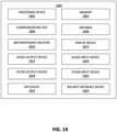
- FIG. 14 is a block diagram of an example computing device 1800 that may include one or more transistor layers with air gapped isolation walls in accordance with any of the embodiments disclosed herein.
- any suitable ones of the components of the computing device 1800 may include a die (e.g., the die 1502 ( FIG. 11B )) having one or more transistor layers with air gapped isolation walls.
- Any one or more of the components of the computing device 1800 may include, or be included in, an IC device 1600 ( FIG. 12 ).
- Any one or more of the components of the computing device 1800 may include, or be included in, an IC device assembly 1700 ( FIG. 13 ).
- FIG. 14 A number of components are illustrated in FIG. 14 as included in the computing device 1800, but any one or more of these components may be omitted or duplicated, as suitable for the application. In some embodiments, some or all of the components included in the computing device 1800 may be attached to one or more motherboards. In some embodiments, some or all of these components are fabricated onto a single system-on-a-chip (SoC) die.
- SoC system-on-a-chip
- the computing device 1800 may not include one or more of the components illustrated in FIG. 14 , but the computing device 1800 may include interface circuitry for coupling to the one or more components.
- the computing device 1800 may not include a display device 1812, but may include display device interface circuitry (e.g., a connector and driver circuitry) to which a display device 1812 may be coupled.
- the computing device 1800 may not include an audio input device 1816 or an audio output device 1814, but may include audio input or output device interface circuitry (e.g., connectors and supporting circuitry) to which an audio input device 1816 or audio output device 1814 may be coupled.
- the computing device 1800 may include a processing device 1802 (e.g., one or more processing devices).
- processing device e.g., one or more processing devices.
- the term "processing device” or “processor” may refer to any device or portion of a device that processes electronic data from registers and/or memory to transform that electronic data into other electronic data that may be stored in registers and/or memory.
- the processing device 1802 may include one or more digital signal processors (DSPs), application-specific integrated circuits (ASICs), central processing units (CPUs), graphics processing units (GPUs), cryptoprocessors (specialized processors that execute cryptographic algorithms within hardware), server processors, or any other suitable processing devices.
- DSPs digital signal processors
- ASICs application-specific integrated circuits
- CPUs central processing units
- GPUs graphics processing units
- cryptoprocessors specialized processors that execute cryptographic algorithms within hardware
- server processors or any other suitable processing devices.
- the computing device 1800 may include a memory 1804, which may itself include one or more memory devices such as volatile memory (e.g., dynamic random access memory (DRAM)), nonvolatile memory (e.g., read-only memory (ROM)), flash memory, solid state memory, and/or a hard drive.
- volatile memory e.g., dynamic random access memory (DRAM)
- nonvolatile memory e.g., read-only memory (ROM)
- flash memory solid state memory
- solid state memory solid state memory
- hard drive e.g., solid state memory, and/or a hard drive.
- the memory 1804 may include memory that shares a die with the processing device 1802. This memory may be used as cache memory and may include embedded dynamic random access memory (eDRAM) or spin transfer torque magnetic random-access memory (STT-MRAM).
- eDRAM embedded dynamic random access memory
- STT-MRAM spin transfer torque magnetic random-access memory
- the computing device 1800 may include a communication chip 1806 (e.g., one or more communication chips).
- the communication chip 1806 may be configured for managing wireless communications for the transfer of data to and from the computing device 1800.
- wireless and its derivatives may be used to describe circuits, devices, systems, methods, techniques, communications channels, etc., that may communicate data through the use of modulated electromagnetic radiation through a nonsolid medium. The term does not imply that the associated devices do not contain any wires, although in some embodiments they might not.
- the communication chip 1806 may implement any of a number of wireless standards or protocols, including but not limited to Institute for Electrical and Electronic Engineers (IEEE) standards including Wi-Fi (IEEE 1402.11 family), IEEE 1402.18 standards (e.g., IEEE 1402.18-2005 Amendment), Long-Term Evolution (LTE) project along with any amendments, updates, and/or revisions (e.g., advanced LTE project, ultramobile broadband (UMB) project (also referred to as "3GPP2”), etc.).
- IEEE 1402.18 compatible Broadband Wireless Access (BWA) networks are generally referred to as WiMAX networks, an acronym that stands for Worldwide Interoperability for Microwave Access, which is a certification mark for products that pass conformity and interoperability tests for the IEEE 1402.18 standards.
- the communication chip 1806 may operate in accordance with a Global System for Mobile Communication (GSM), General Packet Radio Service (GPRS), Universal Mobile Telecommunications System (UMTS), High Speed Packet Access (HSPA), Evolved HSPA (E-HSPA), or LTE network.
- GSM Global System for Mobile Communication
- GPRS General Packet Radio Service
- UMTS Universal Mobile Telecommunications System
- High Speed Packet Access HSPA
- E-HSPA Evolved HSPA
- LTE LTE network.
- the communication chip 1806 may operate in accordance with Enhanced Data for GSM Evolution (EDGE), GSM EDGE Radio Access Network (GERAN), Universal Terrestrial Radio Access Network (UTRAN), or Evolved UTRAN (E-UTRAN).
- EDGE Enhanced Data for GSM Evolution
- GERAN GSM EDGE Radio Access Network
- UTRAN Universal Terrestrial Radio Access Network
- E-UTRAN Evolved UTRAN
- the communication chip 1806 may operate in accordance with Code Division Multiple Access (CDMA), Time Division Multiple Access (TDMA), Digital Enhanced Cordless Telecommunications (DECT), Evolution-Data Optimized (EV-DO), and derivatives thereof, as well as any other wireless protocols that are designated as 3G, 4G, 5G, and beyond.
- CDMA Code Division Multiple Access
- TDMA Time Division Multiple Access
- DECT Digital Enhanced Cordless Telecommunications
- EV-DO Evolution-Data Optimized
- the communication chip 1806 may operate in accordance with other wireless protocols in other embodiments.
- the computing device 1800 may include an antenna 1808 to facilitate wireless communications and/or to receive other wireless communications (such as AM or FM radio transmissions).
- Example 4 provides the IC device of example 2 or 3, where the conductive structure has an upper surface above an interface between the first cap and the first air gap.
- Example 5 provides the IC device of any of examples 2-4 where the conductive structure has an upper surface in a same plane as an upper surface of the first cap.
- Example 8 provides the IC device of any preceding example, where the first transistor and the second transistor are over a front side interconnect layer, the front side interconnect layer including a second conductive structure coupled to the conductive structure.
- Example 9 provides the IC device of example 8, further including a back side interconnect layer over the first transistor and the second transistor, the back side interconnect layer including a third conductive structure coupled to the conductive structure.
- Example 10 provides the IC device of any preceding example, further including a third transistor including a third gate, the third transistor arranged along the gate line, and the third transistor adjacent to the second transistor; and a third air gap between the second gate and the third gate.
- a third transistor including a third gate, the third transistor arranged along the gate line, and the third transistor adjacent to the second transistor; and a third air gap between the second gate and the third gate.
- Example 11 provides an integrated circuit (IC) device including a first transistor layer including a first transistor including a first source or drain region; a second transistor including a second source or drain region, the first source or drain region and the second source or drain region arranged along a first line; a second transistor layer over the first transistor layer, the second transistor layer including a third transistor including a third source or drain region; and a fourth transistor including a fourth source or drain region, the third source or drain region and the fourth source or drain region arranged along a second line; a conductive structure extending through the first transistor layer and the second transistor layer, the conductive structure between the first source or drain region and the second source or drain region; and an air gap between the conductive structure and the first source or drain region.
- IC integrated circuit
- Example 12 provides the IC device of example 11, where the second line is over the first line, and the conductive structure is between the third source or drain region and the fourth source or drain region.
- Example 13 provides the IC device of example 11 or 12, further including a second air gap between the conductive structure and the second source or drain region.
- Example 14 provides the IC device of any of examples 11-13, where the conductive structure is electrically coupled to the second source or drain region of the second transistor.
- Example 15 provides the IC device of example 14, further including a back side interconnect layer over the second transistor layer, where the conductive structure is electrically coupled to an interconnect structure in the back side interconnect layer.
- Example 16 provides the IC device of any of example 11-15, where the first source or drain region includes a first dopant, and the third source or drain region includes a second dopant different from the first dopant.
- Example 17 provides an integrated circuit (IC) device including a first transistor including a first source or drain region; a second transistor including a second source or drain region; an air gap between the first source or drain region and the second source of drain region; a first conductive contact on a front side of the first source or drain region; and a second conductive contact on a back side of the second source or drain region.
- IC integrated circuit
- Example 18 provides the IC device of example 17, further including a dielectric cap over the air gap, the dielectric cap in contact with the second conductive contact.
- Example 19 provides the IC device of example 18, where the second conductive contact has an upper surface in a same plane as an upper surface of the first cap.
- Example 20 provides the IC device of any of examples 17-19, further including a dielectric layer between the first source or drain region and the air gap, the dielectric layer along a side of the first source or drain region.
- Example 21 provides the IC device of any of examples 17-20, further including a back side interconnect layer over the first transistor and the second transistor, the back side interconnect layer including an interconnect structure coupled to the second conductive contact.
- Example 22 provides the IC device of example 21, where the interconnect structure is over a dielectric cap over the air gap.
- Example 23 provides the IC device of example 21 or 22, where the first transistor and the second transistor are over a front side interconnect layer, the front side interconnect layer including a second interconnect structure coupled to the first conductive contact.
- Example 24 provides an IC package that includes an IC die, including one or more of the IC devices according to any one of the preceding examples.
- the IC package may also include a further component, coupled to the IC die.
- Example 25 provides the IC package according to example 24, where the further component is one of a package substrate, a flexible substrate, or an interposer.
- Example 26 provides the IC package according to examples 24 or 25, where the further component is coupled to the IC die via one or more first level interconnects.
- Example 27 provides the IC package according to example 26, where the one or more first level interconnects include one or more solder bumps, solder posts, or bond wires.
- Example 28 provides a computing device that includes a circuit board; and an IC die coupled to the circuit board, where the IC die includes one or more of the transistor/IC devices according to any one of the preceding examples (e.g., transistor/IC devices according to any one of examples 1-23), and/or the IC die is included in the IC package according to any one of the preceding examples (e.g., the IC package according to any one of examples 24-27).
- the IC die includes one or more of the transistor/IC devices according to any one of the preceding examples (e.g., transistor/IC devices according to any one of examples 1-23), and/or the IC die is included in the IC package according to any one of the preceding examples (e.g., the IC package according to any one of examples 24-27).
- Example 29 provides the computing device according to example 28, where the computing device is a wearable computing device (e.g., a smart watch) or hand-held computing device (e.g., a mobile phone).
- the computing device is a wearable computing device (e.g., a smart watch) or hand-held computing device (e.g., a mobile phone).
- Example 30 provides the computing device according to examples 28 or 29, where the computing device is a server processor.
- Example 31 provides the computing device according to examples 28 or 29, where the computing device is a motherboard.
Landscapes
- Thin Film Transistor (AREA)
- Metal-Oxide And Bipolar Metal-Oxide Semiconductor Integrated Circuits (AREA)
Applications Claiming Priority (1)
| Application Number | Priority Date | Filing Date | Title |
|---|---|---|---|
| US18/396,209 US20250210522A1 (en) | 2023-12-26 | 2023-12-26 | Air-gapped isolation walls |
Publications (1)
| Publication Number | Publication Date |
|---|---|
| EP4580334A1 true EP4580334A1 (de) | 2025-07-02 |
Family
ID=93656104
Family Applications (1)
| Application Number | Title | Priority Date | Filing Date |
|---|---|---|---|
| EP24215516.6A Pending EP4580334A1 (de) | 2023-12-26 | 2024-11-26 | Isolationswände mit luftspalt |
Country Status (2)
| Country | Link |
|---|---|
| US (1) | US20250210522A1 (de) |
| EP (1) | EP4580334A1 (de) |
Citations (3)
| Publication number | Priority date | Publication date | Assignee | Title |
|---|---|---|---|---|
| US20200126843A1 (en) * | 2018-10-23 | 2020-04-23 | Taiwan Semiconductor Manufacturing Co., Ltd. | Insulating cap on contact structure and method for forming the same |
| US20200135591A1 (en) * | 2018-10-31 | 2020-04-30 | Taiwan Semiconductor Manufacturing Co., Ltd. | Contact air gap formation and structures thereof |
| US20230387007A1 (en) * | 2022-05-25 | 2023-11-30 | International Business Machines Corporation | Interconnect through gate cut for stacked fet device |
-
2023
- 2023-12-26 US US18/396,209 patent/US20250210522A1/en active Pending
-
2024
- 2024-11-26 EP EP24215516.6A patent/EP4580334A1/de active Pending
Patent Citations (3)
| Publication number | Priority date | Publication date | Assignee | Title |
|---|---|---|---|---|
| US20200126843A1 (en) * | 2018-10-23 | 2020-04-23 | Taiwan Semiconductor Manufacturing Co., Ltd. | Insulating cap on contact structure and method for forming the same |
| US20200135591A1 (en) * | 2018-10-31 | 2020-04-30 | Taiwan Semiconductor Manufacturing Co., Ltd. | Contact air gap formation and structures thereof |
| US20230387007A1 (en) * | 2022-05-25 | 2023-11-30 | International Business Machines Corporation | Interconnect through gate cut for stacked fet device |
Also Published As
| Publication number | Publication date |
|---|---|
| US20250210522A1 (en) | 2025-06-26 |
Similar Documents
| Publication | Publication Date | Title |
|---|---|---|
| US11018264B1 (en) | Three-dimensional nanoribbon-based logic | |
| US20220139911A1 (en) | Use of a placeholder for backside contact formation for transistor arrangements | |
| US20240355682A1 (en) | Extension of nanocomb transistor arrangements to implement gate all around | |
| US11984487B2 (en) | Non-planar transistor arrangements with asymmetric gate enclosures | |
| US12453123B2 (en) | Transistor with front-side and back-side contacts and routing | |
| US20250120143A1 (en) | Extended drain transistor for high voltage applications | |
| US20250113561A1 (en) | Stacked transistors with strain materials on source and drain | |
| US20240321962A1 (en) | Rounded nanoribbons with regrown caps | |
| US20240088035A1 (en) | Full wafer device with back side passive electronic components | |
| US20240234303A9 (en) | Integrated inductor over transistor layer | |
| EP4580334A1 (de) | Isolationswände mit luftspalt | |
| US12513970B2 (en) | Integrated circuits with tungsten interconnect liners | |
| US20230268382A1 (en) | Integrated circuit devices with angled transistors formed based on angled wafers | |
| US20200279939A1 (en) | Transistors including first and second semiconductor materials between source and drain regions and methods of manufacturing the same | |
| US20220399342A1 (en) | Three-dimensional transistor arrangements with recessed gates | |
| US20250210412A1 (en) | Recessed oxide and seam-first etch for air-gapped isolation walls | |
| US20240088029A1 (en) | Full wafer device with back side interconnects and wafer-scale integration | |
| US20260006909A1 (en) | Nanoribbon Transistors Formed from Layered Materials with Dopant for Reduced Strain | |
| US20240088017A1 (en) | Full wafer device with front side passive electronic components | |
| US20240202415A1 (en) | High Density Transistor and Routing Track Architecture | |
| US20250301779A1 (en) | Transistor assemblies with patterned back side-filled isolation regions | |
| US20250212464A1 (en) | Bilayer cavity spacer for gate-all-around transistor | |
| US20250098249A1 (en) | Mitigating proximity effects of deep trench vias | |
| US20250204000A1 (en) | Integrated circuit device with co-metalized electrical contact | |
| US20240321987A1 (en) | Long channel fin transistors in nanoribbon-based devices |
Legal Events
| Date | Code | Title | Description |
|---|---|---|---|
| PUAI | Public reference made under article 153(3) epc to a published international application that has entered the european phase |
Free format text: ORIGINAL CODE: 0009012 |
|
| STAA | Information on the status of an ep patent application or granted ep patent |
Free format text: STATUS: THE APPLICATION HAS BEEN PUBLISHED |
|
| AK | Designated contracting states |
Kind code of ref document: A1 Designated state(s): AL AT BE BG CH CY CZ DE DK EE ES FI FR GB GR HR HU IE IS IT LI LT LU LV MC ME MK MT NL NO PL PT RO RS SE SI SK SM TR |
|
| STAA | Information on the status of an ep patent application or granted ep patent |
Free format text: STATUS: REQUEST FOR EXAMINATION WAS MADE |
|
| 17P | Request for examination filed |
Effective date: 20260102 |