EP4580331A1 - Grabenkondensator in einer verbindungsregion - Google Patents
Grabenkondensator in einer verbindungsregion Download PDFInfo
- Publication number
- EP4580331A1 EP4580331A1 EP24210791.0A EP24210791A EP4580331A1 EP 4580331 A1 EP4580331 A1 EP 4580331A1 EP 24210791 A EP24210791 A EP 24210791A EP 4580331 A1 EP4580331 A1 EP 4580331A1
- Authority
- EP
- European Patent Office
- Prior art keywords
- electrode
- dielectric
- layer
- dielectric layer
- integrated circuit
- Prior art date
- Legal status (The legal status is an assumption and is not a legal conclusion. Google has not performed a legal analysis and makes no representation as to the accuracy of the status listed.)
- Pending
Links
Images





Classifications
-
- H—ELECTRICITY
- H10—SEMICONDUCTOR DEVICES; ELECTRIC SOLID-STATE DEVICES NOT OTHERWISE PROVIDED FOR
- H10D—INORGANIC ELECTRIC SEMICONDUCTOR DEVICES
- H10D1/00—Resistors, capacitors or inductors
- H10D1/01—Manufacture or treatment
- H10D1/041—Manufacture or treatment of capacitors having no potential barriers
- H10D1/042—Manufacture or treatment of capacitors having no potential barriers using deposition processes to form electrode extensions
-
- H—ELECTRICITY
- H10—SEMICONDUCTOR DEVICES; ELECTRIC SOLID-STATE DEVICES NOT OTHERWISE PROVIDED FOR
- H10D—INORGANIC ELECTRIC SEMICONDUCTOR DEVICES
- H10D1/00—Resistors, capacitors or inductors
- H10D1/60—Capacitors
- H10D1/68—Capacitors having no potential barriers
- H10D1/692—Electrodes
- H10D1/711—Electrodes having non-planar surfaces, e.g. formed by texturisation
- H10D1/716—Electrodes having non-planar surfaces, e.g. formed by texturisation having vertical extensions
-
- H—ELECTRICITY
- H10—SEMICONDUCTOR DEVICES; ELECTRIC SOLID-STATE DEVICES NOT OTHERWISE PROVIDED FOR
- H10W—GENERIC PACKAGES, INTERCONNECTIONS, CONNECTORS OR OTHER CONSTRUCTIONAL DETAILS OF DEVICES COVERED BY CLASS H10
- H10W20/00—Interconnections in chips, wafers or substrates
- H10W20/40—Interconnections external to wafers or substrates, e.g. back-end-of-line [BEOL] metallisations or vias connecting to gate electrodes
- H10W20/495—Capacitive arrangements or effects of, or between wiring layers
- H10W20/496—Capacitor integral with wiring layers
Definitions
- an interconnect layer included in a stack of interconnect layers includes a MIM capacitor having a first electrode, a capacitor dielectric on the first electrode, and a second electrode on the capacitor dielectric.
- the MIM capacitor runs along the outside surface of a plurality of dielectric fins, which greatly increases the surface area of the capacitor within a relatively small plan footprint.
- the first and second electrodes may connect with topside contacts or one or more buried conductive lines. Numerous configurations and variations will be apparent in light of this disclosure.
- MIM capacitors Passive metal-insulator-metal (MIM) capacitors protect against power delivery noise and can provide a charge reservoir close to the transistors. Their performance is measured in capacitance/area. Typical MIM capacitors stack electrode and high-K dielectric films in a planar fashion, which makes the capacitance directly dependent on the occupied 2D area. However, it becomes increasingly challenging to integrate such capacitors in densely packed devices with limited available footprint.
- MIM metal-insulator-metal
- the interconnect region includes a stack of interconnect layers having conductive structures for routing signal and power/ground rails between the various semiconductor devices.
- MIM trench capacitors may be formed within one of the interconnect layers to free up more space in the device layer (e.g., where the semiconductor devices are located).
- the trench-based design of the MIM capacitors increases the capacitance due to the increase in surface area without causing a large increase in the plan footprint of the capacitor.
- Various contact designs may be used to form conductive contacts to the MIM capacitor electrodes. Topside contacts and/or vias extending down to bottom-side metal lines may be provided to make electrical contact with the capacitor electrodes.
- an integrated circuit includes a plurality of semiconductor devices, an interconnect region above the plurality of semiconductor devices having a plurality of interconnect layers, and a metal-insulator-metal (MIM) capacitor in the interconnect region.
- the MIM capacitor includes a first electrode running along sidewalls and top surfaces of a plurality of parallel dielectric fins, a capacitor dielectric layer on the first electrode, and a second electrode on the capacitor dielectric layer.
- the capacitor dielectric layer is conformal on the first electrode along the sidewalls and the top surfaces of the plurality of parallel dielectric fins
- the second electrode is conformal on the capacitor dielectric layer along the sidewalls and the top surfaces of the plurality of parallel dielectric fins.
- an electronic device includes a chip package having one or more dies. At least one of the one or more dies includes an interconnect region above a plurality of semiconductor devices and having a plurality of interconnect layers, and a MIM capacitor in an interconnect layer of the plurality of interconnect layers.
- the MIM capacitor includes a first electrode running along sidewalls and top surfaces of a plurality of parallel dielectric fins, a capacitor dielectric layer on the first electrode, and a second electrode on the capacitor dielectric layer.
- the capacitor dielectric layer follows the first electrode along the sidewalls and the top surfaces of the plurality of parallel dielectric fins
- the second electrode follows the capacitor dielectric layer along the sidewalls and the top surfaces of the plurality of parallel dielectric fins.
- an integrated circuit includes a plurality of semiconductor devices, an interconnect region above the plurality of semiconductor devices and having a plurality of stacked interconnect layers, an interconnect layer of the plurality of stacked interconnect layers and having a dielectric layer with a thickness of at least 1 micrometer, and a MIM capacitor embedded in the dielectric layer.
- the MIM capacitor includes a first electrode running along sidewalls and top surfaces of a plurality of parallel dielectric fins, a capacitor dielectric layer on the first electrode, and a second electrode on the capacitor dielectric layer.
- the capacitor dielectric layer follows the first electrode along the sidewalls and the top surfaces of the plurality of parallel dielectric fins
- the second electrode follows the capacitor dielectric layer along the sidewalls and the top surfaces of the plurality of parallel dielectric fins.
- the techniques can be used with any type of planar and non-planar transistors, including finFETs (sometimes called double-gate transistors, or tri-gate transistors), nanowire and nanoribbon transistors (sometimes called gate-all-around transistors), and thin film transistors, to name a few examples.
- the source and drain regions can be, for example, doped portions of a given fin or substrate, or epitaxial regions that are deposited during an etch-and-replace source/drain forming process. The dopant-type in the source and drain regions will depend on the polarity of the corresponding transistor.
- the gate structure can be implemented with a gate-first process or a gate-last process (sometimes called a remove metal gate, or RMG, process).
- any number of semiconductor materials can be used in forming the transistors to which power is being supplied by a buried or backside power rail, such as group IV materials (e.g., silicon, germanium, silicon germanium) or group III-V materials (e.g., gallium arsenide, indium gallium arsenide).
- group IV materials e.g., silicon, germanium, silicon germanium
- group III-V materials e.g., gallium arsenide, indium gallium arsenide.
- Use of the techniques and structures provided herein may be detectable using tools such as electron microscopy including scanning/transmission electron microscopy (SEM/TEM), scanning transmission electron microscopy (STEM), nano-beam electron diffraction (NBD or NBED), and reflection electron microscopy (REM); composition mapping; x-ray crystallography or diffraction (XRD); energy-dispersive x-ray spectroscopy (EDX); secondary ion mass spectrometry (SIMS); time-of-flight SIMS (ToF-SIMS); atom probe imaging or tomography; local electrode atom probe (LEAP) techniques; 3D tomography; or high resolution physical or chemical analysis, to name a few suitable example analytical tools.
- tools such as electron microscopy including scanning/transmission electron microscopy (SEM/TEM), scanning transmission electron microscopy (STEM), nano-beam electron diffraction (NBD or NBED), and reflection electron microscopy (REM); composition mapping; x-ray crystallography or
- such tools may indicate the presence of relatively large (e.g., at least 500 nm in height) accordion-like MIM capacitors within the interconnect region.
- the MIM capacitors may be located within one of the upper layers of the interconnect region (e.g., within the top three interconnect layers of the interconnect region).
- a layer refers to a material portion including a region with a thickness.
- a monolayer is a layer that consists of a single layer of atoms of a given material.
- a layer can extend over the entirety of an underlying or overlying structure, or may have an extent less than the extent of an underlying or overlying structure.
- a layer can be a region of a homogeneous or inhomogeneous continuous structure, with the layer having a thickness less than the thickness of the continuous structure.
- a layer can be located between any pair of horizontal planes between, or at, a top surface and a bottom surface of the continuous structure.
- a layer can extend horizontally, vertically, and/or along a tapered surface.
- a layer can be conformal to a given surface (whether flat or curvilinear) with a relatively uniform thickness across the entire layer.
- compositionally different refers to two materials that have different chemical compositions. This compositional difference may be, for instance, by virtue of an element that is in one material but not the other (e.g., SiGe is compositionally different than silicon), or by way of one material having all the same elements as a second material but at least one of those elements is intentionally provided at a different concentration in one material relative to the other material (e.g., SiGe having 70 atomic percent germanium is compositionally different than from SiGe having 25 atomic percent germanium).
- the materials may also have distinct dopants (e.g., gallium and magnesium) or the same dopants but at differing concentrations.
- compositionally distinct materials may further refer to two materials that have different crystallographic orientations. For instance, (110) silicon is compositionally distinct or different from (100) silicon. Creating a stack of different orientations could be accomplished, for instance, with blanket wafer layer transfer.
- FIG. 1 is a cross-sectional view that illustrates an example portion of an integrated circuit having an interconnect region above a plurality of semiconductor devices, in accordance with an embodiment of the present disclosure.
- the semiconductor devices in this example are non-planar metal oxide semiconductor (MOS) transistors, such as tri-gate or gate-all-around (GAA) transistors, although other transistor topologies and types can also benefit from the techniques provided herein, as will be appreciated (e.g., planar transistors, forksheet transistors, thin film transistors, or any other transistors to which contact can be made).
- MOS metal oxide semiconductor
- GAA gate-all-around
- the integrated circuit includes a device region 101 (sometimes referred to as a device layer), and an interconnect region 103 over the device region 101.
- Device region 101 may include a plurality of semiconductor devices 104 along with one or more other layers or structures associated with the semiconductor devices 104.
- device region 101 can also include one or more dielectric layers 106 that surround active portions or contacts of the semiconductor devices 104.
- Device region 101 may also include one or more conductive contacts 108 that provide electrical contact to transistor elements such as gate structures, drain regions, or source regions.
- Conductive contacts 108 include, for example, tungsten, although other metal or metal alloy materials may be used as well. Conductive contacts may also be a part of, or otherwise include, what is sometimes called a local interconnect, which is considered part of the device layer and usually formed prior to any backend processing.
- device region 101 is formed on or over a substrate 102.
- substrate 102 can be, for example, a bulk substrate including group IV semiconductor material (such as silicon, germanium, or silicon germanium), group III-V semiconductor material (such as gallium arsenide, indium gallium arsenide, or indium phosphide), and/or any other suitable material upon which transistors can be formed.
- the substrate can be a semiconductor-on-insulator substrate having a desired semiconductor layer over a buried insulator layer (e.g., silicon over silicon dioxide).
- Interconnect region 103 includes a plurality of interconnect layers 110a - 110e stacked over one another. Each interconnect layer can include a dielectric material 112 along with one or more different conductive features.
- Dielectric material 112 can be any dielectric, such as silicon oxide, silicon oxycarbide, silicon nitride, or silicon oxynitride. Dielectric material 112 may be deposited using any known dielectric deposition technique such as chemical vapor deposition (CVD), plasma-enhanced chemical vapor deposition (PECVD), flowable CVD, spin-on dielectric, or atomic layer deposition (ALD).
- CVD chemical vapor deposition
- PECVD plasma-enhanced chemical vapor deposition
- ALD atomic layer deposition
- any of conductive traces 114 and conductive vias 116 can include any number of conductive materials, with some examples including copper, ruthenium, tungsten, cobalt, molybdenum, and alloys thereof.
- any of conductive traces 114 and conductive vias 116 include a relatively thin liner or barrier, such as titanium nitride, titanium silicide, tungsten carbo-nitride (WCN), PVD or ALD tungsten, or tantalum nitride.
- any of conductive vias 116 may include a MIM structure as part of the conductive via to provide an anti-fuse element within interconnect region 103.
- each of the various conductive vias 116 and conductive contacts 108 are shown with tapered profiles to indicate a more natural appearance due to the etching process used to form the openings. Any degree of tapering may be observed depending on the etch parameters used and the thickness of the dielectric layer being etched through.
- conductive vias may be stacked one over the other through different dielectric layers of interconnect region 103. However, in some examples, a single via recess may be formed through more than one dielectric layer yielding a taller, more tapered conductive via that extends through two or more dielectric layers.
- the various interconnect layers of interconnect region 103 may not all be the same thickness. According to some embodiments, the interconnect layers increase in thickness moving upwards towards the top of interconnect region 103. Thus, the top-most interconnect layer may have the greatest thickness while the bottom-most interconnect layer may have the smallest thickness. In some examples, the top-most interconnect layer may have a thickness in the range of several micrometers (e.g., 1 - 4 ⁇ m), while the bottom-most interconnect layer may have a thickness of less than 50 nm.
- FIG. 2A illustrates a more detailed cross-section view of a given interconnect layer having a MIM trench capacitor formed within it, according to some embodiments.
- the interconnect layer may include a dielectric layer 202 having a thickness that defines the thickness of the interconnect layer.
- dielectric layer 202 has a total thickness of between about 400 nm and 4000 nm.
- Dielectric layer 202 may be any suitable dielectric material, such as silicon dioxide.
- the illustrated interconnect layer may be one of the upper interconnect layers of interconnect region 103.
- the interconnect layer may be one of the top three interconnect layers of interconnect region 103.
- interconnect layer can also include via structures and metal lines at other locations within the interconnect layer. Other features may also be included. For instance, there may be a relatively thin etch stop layer (e.g., silicon nitride having a thickness in the range of 2 nm to 6 nm) either along the top or bottom surface of dielectric layer 202. Any number of configurations will be apparent in light of this disclosure.
- etch stop layer e.g., silicon nitride having a thickness in the range of 2 nm to 6 nm
- a plurality of dielectric fins 204 are provided within dielectric layer 202.
- Dielectric fins 204 extend lengthwise into and out of the page to form trenches between them.
- dielectric fins 204 have a height between about 200 nm and about 2000 nm.
- Dielectric fins 204 may be formed directly from the dielectric material of dielectric layer 202 (e.g., formed via etching dielectric layer 202), or may be formed from patterning a different dielectric layer deposited on dielectric layer 202.
- a top surface of dielectric fins 204 may be substantially coplanar with a top surface of a remainder of dielectric layer 202.
- the MIM capacitor includes a dielectric material sandwiched between two electrodes.
- the MIM capacitor includes a continuous structure that extends from a first location on the top surface of dielectric layer 206, and along the sidewall and top surfaces of each of the dielectric fins, to a second location on the top surface of dielectric layer 206.
- a first electrode 206 continuously runs along the sidewalls and top surfaces of dielectric fins 204.
- First electrode 206 may also contact a top surface of dielectric layer 202 beyond the trenches, as part of its continuous nature.
- first electrode 206 extends further along the top surface of dielectric layer 202 on one side of the plurality of trenches compared to the other side.
- First contact 208 may include any suitable conductive material, such as tungsten, ruthenium, titanium, tantalum, cobalt, molybdenum, or copper.
- First electrode 206 may be any suitable conductive material, such as tungsten, ruthenium, cobalt, molybdenum, titanium, or copper. First electrode 206 may directly contact the dielectric material of dielectric fins 204 and dielectric layer 202, or a different material may be interposed between first electrode 206 and dielectric fins 204/dielectric layer 202. For example, a barrier layer including tantalum or titanium may be between first electrode 206 and the dielectric material of dielectric fins 204/dielectric layer 202. In another example, a different dielectric layer, such as silicon nitride, may be present between first electrode 206 and the dielectric material of dielectric fins 204/dielectric layer 202. First electrode 206 may have any suitable thickness depending on the application. In some examples, first electrode 206 has a thickness between about 20 nm and about 100 nm.
- a dielectric structure 210 is on first electrode 206 at least within the trenches adjacent to dielectric fins 204. In some examples, dielectric structure 210 follows first electrode 206 along the sidewalls and top surfaces of dielectric fins 204. In some embodiments, dielectric structure 210 also follows at least a portion of first electrode 206 onto a top surface of dielectric layer 202 on either or both sides of the plurality of trenches, as part of its continuous nature. Dielectric structure 210 may represent any number of dielectric layers that make up the capacitor dielectric. According to some embodiments, dielectric structure 210 includes at least one high-k dielectric material, such as a material with a dielectric constant equal to or greater than that of silicon nitride.
- dielectric structure 210 includes a layer of hafnium oxide or aluminum oxide. Dielectric structure 210 may have any suitable thickness depending on the application. In some examples, dielectric structure 210 has a thickness between about 2 nm and about 50 nm.
- a second electrode 212 is on dielectric structure 210 at least within the trenches adjacent to dielectric fins 204.
- second electrode 212 follows dielectric structure 210 along the sidewalls and top surfaces of dielectric fins 204.
- Second electrode 212 may also contact a top surface of dielectric layer 202 beyond the trenches, as part of its continuous nature.
- second electrode 212 extends further along the top surface of dielectric layer 202 on one side of the plurality of trenches compared to the other side.
- the extended portion or tail of second electrode 212 provides a landing site for a second topside contact 214, according to some embodiments.
- Second contact 214 may have similar properties to first contact 208.
- Second electrode 212 may be any suitable conductive material, such as tungsten, ruthenium, cobalt, molybdenum, titanium, or copper.
- first electrode 206 extends further on the top surface of dielectric layer 202 on the left side of the plurality of trenches and second electrode 212 extends further on the top surface of dielectric layer 202 on the right side of the plurality of trenches. Due to the sandwich layout with dielectric structure 210, second electrode 212 is separated from first electrode 206 by dielectric structure 210.
- Second electrode 212 may have any suitable thickness. In some examples, second electrode 212 has a thickness between about 20 nm and about 100 nm.
- the MIM capacitor Due to the continuous capacitor layers extending from a first location on dielectric layer 202, and following the shape of the trenches, to a second location on the dielectric layer 202, the MIM capacitor has a three-dimensional serpentine or accordion shape that increases the surface area between the electrodes within a relatively small two-dimensional footprint, thus requiring less space in the X-direction (left to right on the page) and/or in the Y-direction (into and out of the page). Likewise, another example configuration may use less space in the Z-direction (up and down the page) if more space is used in the X and/or Y directions. Other such variations can be used as well, so as to provide a capacitor structure with a desired amount of capacitance.
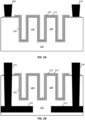
- FIG. 2B illustrates an example where via structures 216 and 218 are formed through at least a portion of a thickness of dielectric layer 202 to contact conductive traces 220 and 222, respectively.
- via structure 216 provides a conductive path between first electrode 206 and conductive trace 220 and via structure 218 provides a conductive path between second electrode 212 and conductive trace 222.
- Via structures 216/218 may include the same conductive materials as contacts 208/214.
- Conductive traces 220/222 may include any suitable conductive material such as tungsten, ruthenium, titanium, tantalum, cobalt, molybdenum, or copper. According to some embodiments, conductive traces 220/222 may be on the same level with each other (e.g., substantially coplanar with each other) beneath dielectric fins 204. Conductive traces 220/222 may be part of the same interconnect layer as the MIM capacitor (e.g., formed within dielectric layer 202), or may be part of a lower interconnect layer beneath dielectric layer 202.
- Figure 2C illustrates another example where second electrode 212 is coupled to topside contact 214, while a conductive trace 224 contacts first electrode 206.
- first electrode 206 directly contacts conductive trace 224 at the bottom of the trenches adjacent to dielectric fins 204.
- Conductive trace 224 may be part of the same interconnect layer as the MIM capacitor (e.g., formed within dielectric layer 202), or may be part of a lower interconnect layer beneath dielectric layer 202.
- Conductive trace 224 may include any suitable conductive material such as tungsten, ruthenium, cobalt, molybdenum, or copper.
- first electrode 206 runs continuously from a first location on the top surface and along side and bottom walls of the recesses to a second location on the top surface of dielectric layer 202.
- capacitor dielectric layer 210 runs continuously along first electrode 206, such that capacitor dielectric layer 210 follows the first electrode at least along the side and bottom walls of the recesses to a third location on the top surface of dielectric layer 202, adjacent to the second location.
- the second electrode 212 runs continuously along capacitor dielectric layer 210, such that second electrode 212 follows capacitor dielectric layer 210 at least along the side and bottom walls of the recesses to a fourth location on the top surface of dielectric layer 202.
- the third location is between the second and fourth locations.
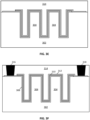
- FIGS 3A - 3F are cross-sectional views that collectively illustrate an example process for forming a portion of an interconnect region of an integrated circuit, in accordance with an embodiment of the present disclosure.
- Each figure shows an example structure that results from the process flow up to that point in time, so the depicted structure evolves as the process flow continues, culminating in the MIM capacitor structure shown in Figure 3F , which is similar to the structure illustrated in Figure 2A .
- Such a structure may be part of an overall integrated circuit (e.g., such as a processor or memory chip) that includes, for example, digital logic cells and/or memory cells and analog mixed signal circuitry.
- the illustrated integrated circuit structure may be part of a larger integrated circuit that includes other integrated circuitry not depicted.
- Example materials and process parameters are given, but the present disclosure is not intended to be limited to any specific such materials or parameters, as will be appreciated.
- Figure 3A is a cross sectional view taken through an interconnect layer of a plurality of stacked interconnect layers. Accordingly, the illustrated interconnect layer may be at any position within interconnect region 103. As noted above, the illustrated interconnect layer may be one of the upper interconnect layers, such as one of the top three interconnect layers of interconnect region 103.
- the interconnect layer includes a dielectric layer 302 that may include any suitable dielectric material, such as silicon dioxide, silicon oxynitride, or silicon oxycarbide. Dielectric layer 302 may be formed using any known dielectric deposition technique, such as CVD, PECVD, flowable CVD, spin-on dielectric, or ALD. Dielectric layer 302 may have a height between about 400 nm and about 4000 nm.
- a plurality of parallel fins 304 are formed within dielectric layer 302.
- An etching process may be performed using a patterned mask to protect some areas of dielectric layer 302 while exposing other areas to be recessed via the etch. Any suitable anisotropic etching process, such as RIE, may be used to form trenches 306 within dielectric layer 302.
- Dielectric fins 304 (and similarly trenches 306) may have a height between about 200 nm and about 2000 nm, depending on the desired size of the capacitor. Other heights may be used as well.
- trenches 306 may have a substantially constant pitch from one another across the page while extending into and out of the page for any desired distance.
- Figure 3B is a cross sectional view of the structure depicted in Figure 3A , after formation of a first electrode 308, according to some embodiments.
- First electrode 308 may include copper or tungsten that is deposited using any one of electroplating, electroless plating, CVD, or PECVD, to name a few examples. Any other suitable conductive materials may be used as well (e.g., aluminum, ruthenium, cobalt, molybdenum).
- first electrode 308 is deposited directly on all surfaces within trenches 306 as well as on the top surfaces of fins 304 and dielectric layer 302.
- barrier layer or other dielectric layer is first deposited on the exposed surfaces of fins 304 and trenches 306, and first electrode 308 is deposited onto the barrier layer or other dielectric layer.
- first electrode 308 is patterned using any suitable lithography process such that first electrode 308 extends further on the top surface of dielectric layer 302 on one side of the plurality of fins compared to the opposite side. In the illustrated example, the left side of first electrode 308 extends further on the top surface of dielectric layer 302 compared to the right side of first electrode 308. According to some embodiments, first electrode 308 is deposited to a thickness between about 20 nm and about 100 nm.
- FIG 3C is a cross sectional view of the structure depicted in Figure 3B , after formation of dielectric structure 310 on first electrode 308, according to some embodiments.
- Dielectric structure 310 may represent any number of deposited dielectric layers.
- dielectric structure 310 includes a layer of hafnium oxide or any other suitable high-k dielectric material.
- Dielectric structure 310 may be deposited using any suitable dielectric deposition technique, such as CVD, PECVD, ALD, or spin-on dielectric.
- dielectric structure 310 follows first electrode 308 over all surfaces within trenches 306 and over fins 304.
- Dielectric structure 310 may be patterned using any suitable lithographic technique such that dielectric structure 310 completely covers the shorter side of first electrode 308 (e.g., at location 309) on the top surface of dielectric layer 302 and exposes a portion of the longer side of first electrode 308 (e.g., at location 311) on the top surface of dielectric layer 302.
- dielectric structure 310 is deposited to a thickness between about 2 nm and about 50 nm.
- Figure 3D is a cross sectional view of the structure depicted in Figure 3C , after formation of a second electrode 312 on dielectric structure 310, according to some embodiments.
- Second electrode 312 may include copper or tungsten that is deposited using any one of electroplating, electroless plating, CVD, or PECVD, to name a few examples. Any other suitable conductive materials may be used as well (e.g., aluminum, ruthenium, cobalt, molybdenum).
- first electrode 308 and second electrode 312 include the same conductive material.
- second electrode 312 follows dielectric structure 310 over all surfaces within trenches 306 and over fins 304.
- second electrode 312 is patterned using any suitable lithography process such that second electrode 312 extends further on the top surface of dielectric layer 302 on one side of the plurality of fins compared to the opposite side.
- the right side of second electrode 312 extends further on the top surface of dielectric layer 302 compared to the right side of second electrode 312.
- first electrode 308 extends further on the top surface of dielectric layer 302 on one side of the plurality of trenches 306 and second electrode 312 extends further on the top surface of dielectric layer 302 on the opposite side of the plurality of trenches 306.
- second electrode 312 is separated from first electrode 308 by dielectric structure 210 along all surfaces within trenches 306 and on fins 304. According to some embodiments, second electrode 312 is deposited to a thickness between about 20 nm and about 100 nm.
- FIG 3E is a cross sectional view of the structure depicted in Figure 3D following the formation of an additional dielectric layer 314 over dielectric layer 302, according to some embodiments.
- Dielectric layer 314 may include any suitable dielectric material, such as the same dielectric material as dielectric layer 302. According to some embodiments, dielectric layer 314 fills in any remaining space within trenches 306 following the formation of the MIM capacitor structure.
- a top surface of dielectric layer 314 may be planarized using any standard polishing technique, such as chemical mechanical polishing (CMP).
- CMP chemical mechanical polishing
- Figure 3F is a cross sectional view of the structure depicted in Figure 3E following the formation of contacts 316/318 through dielectric layer 314, according to some embodiments.
- Contacts 316/318 may include any suitable conductive material, such as tungsten, copper, cobalt, ruthenium, or molybdenum.
- contacts 316/318 include a barrier layer having titanium or tantalum that is deposited first and followed by a metal fill formed on the barrier layer. In the illustrated example, contact 316 makes electrical contact to first electrode 308 and contact 318 makes electrical contact to second electrode 312.
- contacts 316/318 continue through the corresponding first electrode 308 or second electrode 312 to make contact with respective lower conductive traces beneath fins 304 (such as shown in Figure 2B ).
- the lower conductive traces may have been formed within a previous interconnect layer beneath dielectric layer 302, or may have been formed within a portion of dielectric layer 302 prior to the formation of fins 304 and trenches 306.
- contact 316 is omitted and first electrode 308 instead directly contacts a lower conductive trace beneath fins 304 (such as shown in Figure 2C ).
- contact 316 may be formed directly on the lower conductive trace at the bottom of trenches 306. Similar to the above example, the lower conductive trace may have been formed within a previous interconnect layer beneath dielectric layer 302, or may have been formed within a portion of dielectric layer 302 prior to the formation of fins 304 and trenches 306.
- FIG. 4 illustrates an example embodiment of a chip package 400, in accordance with an embodiment of the present disclosure.
- chip package 400 includes one or more dies 402.
- One or more dies 402 may include at least one integrated circuit having a structure as described in any of the aforementioned embodiments.
- One or more dies 402 may include any other circuitry used to interface with other devices formed on the dies, or other devices connected to chip package 400, in some example configurations.
- chip package 400 includes a housing 404 that is bonded to a package substrate 406.
- the housing 404 may be any standard or proprietary housing, and may provide, for example, electromagnetic shielding and environmental protection for the components of chip package 400.
- the one or more dies 402 may be conductively coupled to a package substrate 406 using connections 408, which may be implemented with any number of standard or proprietary connection mechanisms, such as solder bumps, ball grid array (BGA), pins, or wire bonds, to name a few examples.
- Package substrate 406 may be any standard or proprietary package substrate, but in some cases includes a dielectric material having conductive pathways (e.g., including conductive vias and lines) extending through the dielectric material between the faces of package substrate 406, or between different locations on each face.
- package substrate 406 may have a thickness less than 1 millimeter (e.g., between 0.1 millimeters and 0.5 millimeters), although any number of package geometries can be used. Additional conductive contacts 412 may be disposed at an opposite face of package substrate 406 for conductively contacting, for instance, a printed circuit board (PCB). One or more vias 410 extend through a thickness of package substrate 406 to provide conductive pathways between one or more of connections 408 to one or more of contacts 412.
- PCB printed circuit board
- Vias 410 are illustrated as single straight columns through package substrate 406 for ease of illustration, although other configurations can be used (e.g., damascene, dual damascene, through-silicon via, or an interconnect structure that meanders through the thickness of substrate 406 to contact one or more intermediate locations therein). In still other embodiments, vias 410 are fabricated by multiple smaller stacked vias, or are staggered at different locations across package substrate 406.
- contacts 412 are solder balls (e.g., for bump-based connections or a ball grid array arrangement), but any suitable package bonding mechanism may be used (e.g., pins in a pin grid array arrangement or lands in a land grid array arrangement). In some embodiments, a solder resist is disposed between contacts 412, to inhibit shorting.
- a mold material 414 may be disposed around the one or more dies 402 included within housing 404 (e.g., between dies 402 and package substrate 406 as an underfill material, as well as between dies 402 and housing 404 as an overfill material). Although the dimensions and qualities of the mold material 414 can vary from one embodiment to the next, in some embodiments, a thickness of mold material 414 is less than 1 millimeter.
- Example materials that may be used for mold material 414 include epoxy mold materials, as suitable. In some cases, the mold material 414 is thermally conductive, in addition to being electrically insulating.
- FIG. 5 is an example computing system implemented with one or more of the integrated circuit structures as disclosed herein, in accordance with some embodiments of the present disclosure.
- the computing system 500 houses a motherboard 502.
- the motherboard 502 may include a number of components, including, but not limited to, a processor 504 and at least one communication chip 506, each of which can be physically and electrically coupled to the motherboard 502, or otherwise integrated therein.
- the motherboard 502 may be, for example, any printed circuit board (PCB), whether a main board, a daughterboard mounted on a main board, or the only board of system 500, etc.
- PCB printed circuit board
- computing system 500 may include one or more other components that may or may not be physically and electrically coupled to the motherboard 502. These other components may include, but are not limited to, volatile memory (e.g., DRAM), non-volatile memory (e.g., ROM), a graphics processor, a digital signal processor, a crypto processor, a chipset, an antenna, a display, a touchscreen display, a touchscreen controller, a battery, an audio codec, a video codec, a power amplifier, a global positioning system (GPS) device, a compass, an accelerometer, a gyroscope, a speaker, a camera, and a mass storage device (such as hard disk drive, compact disk (CD), digital versatile disk (DVD), and so forth).
- volatile memory e.g., DRAM
- non-volatile memory e.g., ROM
- graphics processor e.g., a digital signal processor
- crypto processor e.g., a graphics processor
- a digital signal processor
- any of the components included in computing system 500 may include one or more integrated circuit structures or devices configured in accordance with an example embodiment (e.g., a module including an integrated circuit having interconnect structures that have one or more MIM trench capacitors in the interconnect region).
- multiple functions can be integrated into one or more chips (e.g., for instance, note that the communication chip 506 can be part of or otherwise integrated into the processor 504).
- the communication chip 506 enables wireless communications for the transfer of data to and from the computing system 500.
- wireless and its derivatives may be used to describe circuits, devices, systems, methods, techniques, communications channels, etc., that may communicate data through the use of modulated electromagnetic radiation through a non-solid medium. The term does not imply that the associated devices do not contain any wires, although in some embodiments they might not.
- the communication chip 506 may implement any of a number of wireless standards or protocols, including, but not limited to, Wi-Fi (IEEE 802.11 family), WiMAX (IEEE 802.16 family), IEEE 802.20, long term evolution (LTE), Ev-DO, HSPA+, HSDPA+, HSUPA+, EDGE, GSM, GPRS, CDMA, TDMA, DECT, Bluetooth, derivatives thereof, as well as any other wireless protocols that are designated as 3G, 4G, 5G, and beyond.
- the computing system 500 may include a plurality of communication chips 506.
- a first communication chip 506 may be dedicated to shorter range wireless communications such as Wi-Fi and Bluetooth and a second communication chip 506 may be dedicated to longer range wireless communications such as GPS, EDGE, GPRS, CDMA, WiMAX, LTE, Ev-DO, and others.
- the processor 504 of the computing system 500 includes an integrated circuit die packaged within the processor 504.
- the integrated circuit die of the processor includes onboard circuitry that is implemented with one or more semiconductor devices as variously described herein.
- the term "processor" may refer to any device or portion of a device that processes, for instance, electronic data from registers and/or memory to transform that electronic data into other electronic data that may be stored in registers and/or memory.
- the communication chip 506 also may include an integrated circuit die packaged within the communication chip 506.
- the integrated circuit die of the communication chip includes one or more semiconductor devices as variously described herein.
- multi-standard wireless capability may be integrated directly into the processor 504 (e.g., where functionality of any chips 506 is integrated into processor 504, rather than having separate communication chips).
- processor 504 may be a chip set having such wireless capability.
- any number of processor 504 and/or communication chips 506 can be used.
- any one chip or chip set can have multiple functions integrated therein.
- the computing system 500 may be a laptop, a netbook, a notebook, a smartphone, a tablet, a personal digital assistant (PDA), an ultra-mobile PC, a mobile phone, a desktop computer, a server, a printer, a scanner, a monitor, a set-top box, an entertainment control unit, a digital camera, a portable music player, a digital video recorder, or any other electronic device that processes data or employs one or more integrated circuit structures or devices formed using the disclosed techniques, as variously described herein.
- PDA personal digital assistant
- the various components of the computing system 500 may be combined or integrated in a system-on-a-chip (SoC) architecture.
- the components may be hardware components, firmware components, software components or any suitable combination of hardware, firmware or software.
- Example 1 is an integrated circuit that includes a plurality of semiconductor devices, an interconnect region above the plurality of semiconductor devices having a plurality of interconnect layers, and a metal-insulator-metal (MIM) capacitor in the interconnect region.
- the MIM capacitor includes a first electrode running along sidewalls and top surfaces of a plurality of parallel dielectric fins, a capacitor dielectric layer on the first electrode, and a second electrode on the capacitor dielectric layer.
- the capacitor dielectric layer is conformal on the first electrode along the sidewalls and the top surfaces of the plurality of parallel dielectric fins
- the second electrode is conformal on the capacitor dielectric layer along the sidewalls and the top surfaces of the plurality of parallel dielectric fins.
- Example 2 includes the integrated circuit of Example 1, wherein each of the plurality of parallel dielectric fins have a height greater than 1 micrometer.
- Example 3 includes the integrated circuit of Example 1 or 2, wherein the plurality of parallel dielectric fins are part of a dielectric layer in an interconnect layer of the plurality of interconnect layers.
- Example 4 includes the integrated circuit of Example 3, wherein the top surfaces of the plurality of parallel dielectric fins are substantially coplanar with a top surface of the dielectric layer.
- Example 5 includes the integrated circuit of Example 3 or 4, wherein the first electrode extends along a top surface of the dielectric layer on one side of the plurality of parallel dielectric fins and the second electrode extends along a top surface of the dielectric layer on an opposite side of the plurality of parallel dielectric fins.
- Example 6 includes the integrated circuit of Example 5, further comprising a first conductive contact on the first electrode over the top surface of the dielectric layer, and a second conductive contact on the second electrode over the top surface of the dielectric layer.
- Example 7 includes the integrated circuit of Example 5, further comprising a first conductive layer and a second conductive layer, both beneath the MIM capacitor, wherein a first conductive via extends from the first electrode on the top surface of the dielectric layer to the first conductive layer, and a second conductive via extends from the second electrode on the top surface of the dielectric layer to the second conductive layer.
- Example 8 includes the integrated circuit of any one of Examples 3-5, further comprising a conductive layer beneath the MIM capacitor and in contact with the first electrode.
- Example 9 includes the integrated circuit of Example 8, wherein the second electrode extends along a top surface of the dielectric layer on one side of the plurality of parallel dielectric fins, and the integrated circuit further comprises a conductive contact on the second electrode over the top surface of the dielectric layer.
- Example 11 includes the integrated circuit of any one of Examples 1-10, wherein the capacitor dielectric includes a high-k dielectric.
- Example 12 includes the integrated circuit of any one of Examples 1-11, wherein the MIM capacitor is in more than one interconnect layer of the plurality of interconnect layers.
- Example 13 includes the integrated circuit of any one of Examples 1-12, wherein the plurality of parallel dielectric fins includes three to ten parallel dielectric fins.
- Example 14 includes the integrated circuit of any one of Examples 1-13, wherein the plurality of parallel dielectric fins define a first trench and a second trench, with one of the dielectric fins between the first trench and the second trench, and wherein the first electrode continuously runs along sidewalls of the first and second trenches and the top surfaces of the dielectric fin between the first and second trenches.
- Example 15 is a printed circuit board that includes the integrated circuit of any one of Examples 1-14.
- Example 16 is an electronic device that includes a chip package having one or more dies. At least one of the one or more dies includes an interconnect region above a plurality of semiconductor devices and having a plurality of interconnect layers, and a metal-insulator-metal (MIM) capacitor in an interconnect layer of the plurality of stacked interconnect layers.
- the MIM capacitor includes a first electrode running along sidewalls and top surfaces of a plurality of parallel dielectric fins, a capacitor dielectric layer on the first electrode, and a second electrode on the capacitor dielectric layer.
- the capacitor dielectric layer follows the first electrode along the sidewalls and the top surfaces of the plurality of parallel dielectric fins
- the second electrode follows the capacitor dielectric layer along the sidewalls and the top surfaces of the plurality of parallel dielectric fins.
- Example 17 includes the electronic device of Example 16, wherein the plurality of parallel dielectric fins have a height greater than 1 micrometer.
- Example 18 includes the electronic device of Example 16 or 17, wherein the interconnect layer comprises a dielectric layer and the plurality of parallel dielectric fins are part of the dielectric layer.
- Example 21 includes the electronic device of Example 19, wherein the at least one of the one or more dies further comprises a first conductive layer beneath the MIM capacitor and a second conductive layer beneath the MIM capacitor.
- a first conductive via extends from the first electrode on the top surface of the dielectric layer to the first conductive layer, and a second conductive via extends from the second electrode on the top surface of the dielectric layer to the second conductive layer.
- Example 23 includes the electronic device of Example 22, wherein the second electrode extends along a top surface of the dielectric layer on one side of the plurality of parallel dielectric fins, and the at least one of the one or more dies further comprises a conductive contact on the second electrode over the top surface of the dielectric layer.
- Example 24 includes the electronic device of any one of Examples 16-23, wherein the interconnect layer is one of the three topmost interconnect layers of the plurality of interconnect layers.
- Example 25 includes the electronic device of any one of Examples 16-24, further comprising a printed circuit board, wherein the chip package is attached to the printed circuit board.
- Example 26 is an integrated circuit that includes a plurality of semiconductor devices, an interconnect region above the plurality of semiconductor devices and having a plurality of interconnect layers, an interconnect layer of the plurality of stacked interconnect layers, and a metal-insulator-metal (MIM) capacitor embedded in the dielectric layer.
- the interconnect layer includes a dielectric layer having a thickness of at least 1 micrometer.
- the MIM capacitor includes a first electrode running along sidewalls and top surfaces of a plurality of parallel dielectric fins, a capacitor dielectric layer on the first electrode, and a second electrode on the capacitor dielectric layer.
- the capacitor dielectric layer follows the first electrode along the sidewalls and the top surfaces of the plurality of parallel dielectric fins.
- the second electrode follows the capacitor dielectric layer along the sidewalls and the top surfaces of the plurality of parallel dielectric fins.
- Example 27 includes the integrated circuit of Example 26, wherein the top surfaces of the plurality of parallel dielectric fins are substantially coplanar with a top surface of the dielectric layer.
- Example 28 includes the integrated circuit of Example 26 or 27, wherein the first electrode extends along a top surface of the dielectric layer on one side of the plurality of parallel dielectric fins and the second electrode extends along a top surface of the dielectric layer on an opposite side of the plurality of parallel dielectric fins.
- Example 29 includes the integrated circuit of Example 28, further comprising a first conductive contact on the first electrode over the top surface of the dielectric layer, and a second conductive contact on the second electrode over the top surface of the dielectric layer.
- Example 30 includes the integrated circuit of Example 28, further comprising a first conductive layer and a second conductive layer beneath the MIM capacitor, wherein a first conductive via extends from the first electrode on the top surface of the dielectric layer to the first conductive layer, and a second conductive via extends from the second electrode on the top surface of the dielectric layer to the second conductive layer.
- Example 31 includes the integrated circuit of any one of Examples 26-28, further comprising a conductive layer beneath the MIM capacitor and in contact with the first electrode.
- Example 32 includes the integrated circuit of Example 31, wherein the second electrode extends along a top surface of the dielectric layer on one side of the plurality of parallel dielectric fins, and the integrated circuit further comprises a conductive contact on the second electrode over the top surface of the dielectric layer.
- Example 33 includes the integrated circuit of any one of Examples 26-32, wherein the interconnect layer is one of the three topmost interconnect layers of the plurality of interconnect layers.
- Example 34 is a printed circuit board that includes the integrated circuit of any one of Examples 26-33.
- Example 35 is an integrated circuit that includes an interconnect layer having a conductive interconnect feature within a layer of dielectric material, and a metal-insulator-metal (MIM) capacitor.
- the conductive interconnect feature is a conductive via or a conductive line.
- the interconnect layer further includes a first recess and a second recess with each recess extending from a top surface of the layer of dielectric material toward a bottom surface of the layer of dielectric material.
- the MIM capacitor includes a first electrode that runs continuously from a first location on the top surface and along side and bottom walls of the first and second recesses to a second location on the top surface, a capacitor dielectric layer that runs continuously along the first electrode, and a second electrode that runs continuously along the capacitor dielectric layer.
- the capacitor dielectric layer follows the first electrode at least along the side and bottom walls of the first and second recesses to a third location on the top surface.
- the second electrode follows the capacitor dielectric layer at least along the side and bottom walls of the first and second recesses to a fourth location on the top surface.
- the third location is between the second and fourth locations.
- Example 36 includes the integrated circuit of Example 35, wherein each of the first and second recesses has a height greater than 1 micrometer.
- Example 37 includes the integrated circuit of Example 35 or 36, further comprising a first conductive contact on the first electrode, and a second conductive contact on the second electrode.
- Example 38 includes the integrated circuit of Example 35 or 36, further comprising a first conductive layer and a second conductive layer, both beneath the MIM capacitor, wherein a first conductive via extends from the first electrode to the first conductive layer, and a second conductive via extends from the second electrode to the second conductive layer.
- Example 42 includes the integrated circuit of any one of Examples 35-41, wherein the capacitor dielectric includes a high-k dielectric.
Landscapes
- Semiconductor Integrated Circuits (AREA)
- Engineering & Computer Science (AREA)
- Power Engineering (AREA)
Applications Claiming Priority (1)
| Application Number | Priority Date | Filing Date | Title |
|---|---|---|---|
| US18/397,682 US20250218928A1 (en) | 2023-12-27 | 2023-12-27 | Trench capacitor in interconnect region |
Publications (1)
| Publication Number | Publication Date |
|---|---|
| EP4580331A1 true EP4580331A1 (de) | 2025-07-02 |
Family
ID=93430524
Family Applications (1)
| Application Number | Title | Priority Date | Filing Date |
|---|---|---|---|
| EP24210791.0A Pending EP4580331A1 (de) | 2023-12-27 | 2024-11-05 | Grabenkondensator in einer verbindungsregion |
Country Status (2)
| Country | Link |
|---|---|
| US (1) | US20250218928A1 (de) |
| EP (1) | EP4580331A1 (de) |
Families Citing this family (1)
| Publication number | Priority date | Publication date | Assignee | Title |
|---|---|---|---|---|
| US20250113498A1 (en) * | 2023-10-02 | 2025-04-03 | International Business Machines Corporation | Metal spacer 3d-mim capacitor |
Citations (4)
| Publication number | Priority date | Publication date | Assignee | Title |
|---|---|---|---|---|
| US20030183862A1 (en) * | 2002-03-26 | 2003-10-02 | Samsung Electronics Co., Ltd. | Semiconductor device having metal-insulator-metal capacitor and fabrication method thereof |
| US20230163063A1 (en) * | 2021-11-19 | 2023-05-25 | Intel Corporation | Staircase-based metal-insulator-metal (mim) capacitors |
| US20230178588A1 (en) * | 2021-12-06 | 2023-06-08 | International Business Machines Corporation | Metal-insulator-metal capacitor structure with enlarged capacitor area |
| US20230411443A1 (en) * | 2022-06-16 | 2023-12-21 | Intel Corporation | Metal insulator metal (mim) capacitor architectures |
-
2023
- 2023-12-27 US US18/397,682 patent/US20250218928A1/en active Pending
-
2024
- 2024-11-05 EP EP24210791.0A patent/EP4580331A1/de active Pending
Patent Citations (4)
| Publication number | Priority date | Publication date | Assignee | Title |
|---|---|---|---|---|
| US20030183862A1 (en) * | 2002-03-26 | 2003-10-02 | Samsung Electronics Co., Ltd. | Semiconductor device having metal-insulator-metal capacitor and fabrication method thereof |
| US20230163063A1 (en) * | 2021-11-19 | 2023-05-25 | Intel Corporation | Staircase-based metal-insulator-metal (mim) capacitors |
| US20230178588A1 (en) * | 2021-12-06 | 2023-06-08 | International Business Machines Corporation | Metal-insulator-metal capacitor structure with enlarged capacitor area |
| US20230411443A1 (en) * | 2022-06-16 | 2023-12-21 | Intel Corporation | Metal insulator metal (mim) capacitor architectures |
Also Published As
| Publication number | Publication date |
|---|---|
| US20250218928A1 (en) | 2025-07-03 |
Similar Documents
| Publication | Publication Date | Title |
|---|---|---|
| US12342614B2 (en) | Asymmetric gate structures and contacts for stacked transistors | |
| US20240113104A1 (en) | Forksheet transistor structures with gate cut spine | |
| EP4580331A1 (de) | Grabenkondensator in einer verbindungsregion | |
| US20260114030A1 (en) | Forming metal gate cuts using multiple passes for depth control | |
| US20250336800A1 (en) | Decoupling capacitors using backside connections | |
| CN120640781A (zh) | 背侧交叉耦合互连 | |
| KR20240085842A (ko) | finFET 디바이스와 게이트-올-어라운드 디바이스의 통합 | |
| EP4661079A1 (de) | Planare und 3d-kondensatoren in einem verbindungsbereich | |
| EP4576208A1 (de) | Mit durchkontaktierungsstrukturen integrierte kondensatoren | |
| US20250300077A1 (en) | End-to-end reduction between semiconductor interconnects | |
| US20250372482A1 (en) | Through semiconductor via as a well tap structure | |
| EP4694624A1 (de) | Versetzte vorder- und rückseitenverbindungsbahnen einer standardeinheitszelle | |
| US20250218931A1 (en) | Interconnect via with induced asymmetric profile | |
| US20250201698A1 (en) | Offset via fuse structure in interconnect region | |
| EP4718984A2 (de) | Zellenarchitektur mit gabelblatt- und tor-all-around-vorrichtungen | |
| EP4485532A1 (de) | Versetzte via architektur über einheitszellen hinweg | |
| US20250364369A1 (en) | Dielectric socket to facilitate through-semiconductor via structure | |
| EP4622418A1 (de) | In einem gate-graben begrenzter gate-schnitt | |
| EP4576087A1 (de) | Rückseiten-logikverbindungen | |
| TW202612487A (zh) | 互連區域中的平面電容及三維電容 | |
| EP4246564A1 (de) | Partielle gate-cut-strukturen in einer integrierten schaltung | |
| US20240355891A1 (en) | Conductive bridge through dielectric wall between source or drain contacts | |
| CN118693047A (zh) | 桥接接触结构 | |
| CN121510664A (zh) | 具有耦合的背侧触点的堆叠的半导体器件 | |
| CN118693086A (zh) | 栅极切口与深背面过孔之间的半导体器件 |
Legal Events
| Date | Code | Title | Description |
|---|---|---|---|
| PUAI | Public reference made under article 153(3) epc to a published international application that has entered the european phase |
Free format text: ORIGINAL CODE: 0009012 |
|
| STAA | Information on the status of an ep patent application or granted ep patent |
Free format text: STATUS: THE APPLICATION HAS BEEN PUBLISHED |
|
| AK | Designated contracting states |
Kind code of ref document: A1 Designated state(s): AL AT BE BG CH CY CZ DE DK EE ES FI FR GB GR HR HU IE IS IT LI LT LU LV MC ME MK MT NL NO PL PT RO RS SE SI SK SM TR |
|
| STAA | Information on the status of an ep patent application or granted ep patent |
Free format text: STATUS: REQUEST FOR EXAMINATION WAS MADE |
|
| 17P | Request for examination filed |
Effective date: 20251223 |