EP4579699A2 - Multilayer electronic component comprising a crack extending to an inside of the body from an end of one of the external electrodes - Google Patents
Multilayer electronic component comprising a crack extending to an inside of the body from an end of one of the external electrodes Download PDFInfo
- Publication number
- EP4579699A2 EP4579699A2 EP24210833.0A EP24210833A EP4579699A2 EP 4579699 A2 EP4579699 A2 EP 4579699A2 EP 24210833 A EP24210833 A EP 24210833A EP 4579699 A2 EP4579699 A2 EP 4579699A2
- Authority
- EP
- European Patent Office
- Prior art keywords
- overlapping region
- electronic component
- multilayer electronic
- electrode
- internal electrode
- Prior art date
- Legal status (The legal status is an assumption and is not a legal conclusion. Google has not performed a legal analysis and makes no representation as to the accuracy of the status listed.)
- Pending
Links
Images



Classifications
-
- H—ELECTRICITY
- H01—ELECTRIC ELEMENTS
- H01G—CAPACITORS; CAPACITORS, RECTIFIERS, DETECTORS, SWITCHING DEVICES, LIGHT-SENSITIVE OR TEMPERATURE-SENSITIVE DEVICES OF THE ELECTROLYTIC TYPE
- H01G4/00—Fixed capacitors; Processes of their manufacture
- H01G4/30—Stacked capacitors
-
- H—ELECTRICITY
- H01—ELECTRIC ELEMENTS
- H01G—CAPACITORS; CAPACITORS, RECTIFIERS, DETECTORS, SWITCHING DEVICES, LIGHT-SENSITIVE OR TEMPERATURE-SENSITIVE DEVICES OF THE ELECTROLYTIC TYPE
- H01G2/00—Details of capacitors not covered by a single one of groups H01G4/00-H01G11/00
- H01G2/02—Mountings
- H01G2/06—Mountings specially adapted for mounting on a printed-circuit support
-
- H—ELECTRICITY
- H01—ELECTRIC ELEMENTS
- H01G—CAPACITORS; CAPACITORS, RECTIFIERS, DETECTORS, SWITCHING DEVICES, LIGHT-SENSITIVE OR TEMPERATURE-SENSITIVE DEVICES OF THE ELECTROLYTIC TYPE
- H01G4/00—Fixed capacitors; Processes of their manufacture
- H01G4/002—Details
- H01G4/005—Electrodes
- H01G4/008—Selection of materials
- H01G4/0085—Fried electrodes
-
- H—ELECTRICITY
- H01—ELECTRIC ELEMENTS
- H01G—CAPACITORS; CAPACITORS, RECTIFIERS, DETECTORS, SWITCHING DEVICES, LIGHT-SENSITIVE OR TEMPERATURE-SENSITIVE DEVICES OF THE ELECTROLYTIC TYPE
- H01G4/00—Fixed capacitors; Processes of their manufacture
- H01G4/002—Details
- H01G4/005—Electrodes
- H01G4/012—Form of non-self-supporting electrodes
-
- H—ELECTRICITY
- H01—ELECTRIC ELEMENTS
- H01G—CAPACITORS; CAPACITORS, RECTIFIERS, DETECTORS, SWITCHING DEVICES, LIGHT-SENSITIVE OR TEMPERATURE-SENSITIVE DEVICES OF THE ELECTROLYTIC TYPE
- H01G4/00—Fixed capacitors; Processes of their manufacture
- H01G4/002—Details
- H01G4/228—Terminals
-
- H—ELECTRICITY
- H01—ELECTRIC ELEMENTS
- H01G—CAPACITORS; CAPACITORS, RECTIFIERS, DETECTORS, SWITCHING DEVICES, LIGHT-SENSITIVE OR TEMPERATURE-SENSITIVE DEVICES OF THE ELECTROLYTIC TYPE
- H01G4/00—Fixed capacitors; Processes of their manufacture
- H01G4/002—Details
- H01G4/228—Terminals
- H01G4/232—Terminals electrically connecting two or more layers of a stacked or rolled capacitor
-
- H—ELECTRICITY
- H01—ELECTRIC ELEMENTS
- H01G—CAPACITORS; CAPACITORS, RECTIFIERS, DETECTORS, SWITCHING DEVICES, LIGHT-SENSITIVE OR TEMPERATURE-SENSITIVE DEVICES OF THE ELECTROLYTIC TYPE
- H01G4/00—Fixed capacitors; Processes of their manufacture
- H01G4/002—Details
- H01G4/018—Dielectrics
- H01G4/06—Solid dielectrics
- H01G4/08—Inorganic dielectrics
- H01G4/12—Ceramic dielectrics
- H01G4/1209—Ceramic dielectrics characterised by the ceramic dielectric material
- H01G4/1218—Ceramic dielectrics characterised by the ceramic dielectric material based on titanium oxides or titanates
- H01G4/1227—Ceramic dielectrics characterised by the ceramic dielectric material based on titanium oxides or titanates based on alkaline earth titanates
Definitions
- the present disclosure relates to a multilayer electronic component.
- MLCCs may include a body and an external electrode disposed on the body.
- the stress tends to be concentrated on an end of the external electrode, and accordingly, a crack may occur from end of the external electrode toward the inside of the body.
- a short circuit may occur in the MLCC.
- a method of reducing the number of laminated internal electrodes or reducing a size of the overlapping region may be considered, but reducing the number of laminated internal electrodes or the size of the overlapping region may lower capacitance of an MLCC and DC-bias properties.
- an MLCC having excellent electrical properties such as capacitance and DC-bias while preventing short circuits from occurring due to a crack propagating to an overlapping region of a body.
- Another aspect of the present disclosure provides a multilayer electronic component having excellent electrical properties such as capacitance or the like.
- the body may include an overlapping region in which the first internal electrode overlaps the second internal electrode adjacent thereto in the first direction with the dielectric layer interposed therebetween.
- a length in the second direction of a central portion of the overlapping region in the first direction may be greater than that of both ends of the overlapping region in the first direction.
- the body may have a crack extending to the inside of the body from an end of at least one of the first and second external electrodes, the crack spaced apart from the overlapping region.
- the multilayer electronic component 100 has a structure in which the central portion of the overlapping region 110a in the first direction, having a longer distance from the crack CR, has a length in the second direction longer than that of both ends of the overlapping region 110a, having a shorter distance from the crack CR, thereby preventing the crack CR from propagating to the inside of the overlapping region 110a to prevent a short circuit defect from occurring, and improving capacitance and DC-bias properties of the multilayer electronic component 100 as compared to a case in which an overall length of the overlapping region 110a in the second direction is reduced.
- a length in the second direction in which the first external electrode 131 and the second internal electrode 122 are spaced apart from each other may gradually increase from the central portion of the overlapping region 110a in the first direction to both ends of the overlapping region 110a in the first direction
- a length in the second direction in which the second external electrode 132 and the first internal electrode 121 are spaced apart from each other may gradually increase from the central portion of the overlapping region 110a in the first direction to both ends of the overlapping region 110a in the first direction.
- a distance in the second direction between the overlapping region 110a and the crack CR may gradually increase from both ends of the overlapping region 110a in the first direction toward the central portion of the overlapping region 110a in the first direction, but the present disclosure is not limited thereto.
- the crack CR propagating from the ends 131a and 132a of the external electrodes to the inside of the body 110, may easily occur as high pressure is applied to the multilayer electronic component 100.
- LE is shorter than the LM in order to prevent a short circuit defect from occurring due to the crack CR from extending to the inside of the overlapping region 110a, flexural strength of a high-pressure electronic component may not be ensured.
- the crack surface may be the second surface.
- One end of the crack CR, present on the end 131a of the first external electrode, may be positioned on the second surface, and the other end of the crack CR may be positioned on the third surface 3.
- ⁇ may be, for example, 60° to 70°.
- the body 110 may include a first dummy electrode 123 disposed to be spaced apart from the second internal electrode 122 in the second direction, the first dummy electrode 123 connected to the first external electrode 131, and a second dummy electrode 124 disposed to be spaced apart from the first internal electrode 121 in the second direction, the second dummy electrode 124 connected to the second external electrode 132.
- the first dummy electrode 123 may be substantially coplanar with the second internal electrode 122
- the second dummy electrode 124 may be substantially coplanar with the first internal electrode 121.
- the dummy electrodes 123 and 124 may be appropriately formed on the body 110, such that a multilayer electronic component according to an example embodiment of the present disclosure may be manufactured without increasing a type of internal electrode pattern printed on a ceramic green sheet to be described below.
- a length of the first dummy electrode 123 in the second direction, measured in the central portion of the overlapping region 110a in the first direction may be shorter than a length of the first dummy electrode 123 in the second direction, measured in both ends of the overlapping region 110a in the first direction.
- a length of the second dummy electrode 124 in the second direction, measured in the central portion of the overlapping region 110a in the first direction may be shorter than a length of the second dummy electrode 124 in the second direction, measured in both ends of the overlapping region 110a in the first direction.
- the length of the first dummy electrode 123 in the second direction may increase from a center of the body 110 in the first direction toward an outer portion of the body 110 in the first direction
- the length of the second dummy electrode 124 in the second direction may increase from the center of the body 110 in the first direction toward the outer portion of the body 110 in the first direction
- a gap between the first dummy electrode 123 and the second internal electrode 122 in the second direction may be substantially constant from a topmost first dummy electrode to a bottommost first dummy electrode.
- a gap between the second dummy electrode 124 and the first internal electrode 121 in the second direction may be substantially constant from a topmost second dummy electrode to a bottommost second dummy electrode.
- a ratio (LD/LM) of LD to LM may be 0.3 or more.
- LD/LM is less than 0.3, the second internal electrode 122 and the first dummy electrode 123 may come into contact with each other to cause a short circuit defect.
- An upper limit of LD/LM is not particularly limited, but may be 0.8 or less.
- ceramic powder particles for forming ceramic green sheets 211a and 211b may be prepared.
- the ceramic powder particles may be (Ba 1-x Ca x )TiO 3 (0 ⁇ x ⁇ 1), Ba(Ti 1-y Ca y )O 3 (0 ⁇ y ⁇ 1), (Ba 1-x Ca x )(Ti 1-y Zr y )O 3 (0 ⁇ x ⁇ 1, 0 ⁇ y ⁇ 1), or Ba (Ti 1-y Zr y )O 3 (0 ⁇ y ⁇ 1) obtained by partially dissolving Ca or Zr in BaTiO 3 .
- BaTiO 3 powder particles may be synthesized, for example, by reacting a titanium raw material such as titanium dioxide with a barium raw material such as barium carbonate.
- a method of synthesizing the ceramic powder particles may include, for example, a solid-phase method, a sol-gel method, and a hydrothermal synthesis method, but the present disclosure is not limited thereto.
- the prepared ceramic powder particles may be dried and ground, an organic solvent such as ethanol and a binder such as polyvinyl butyral may be mixed to prepare a ceramic slurry, and then the ceramic slurry may be coated and dried on a carrier film to prepare the ceramic green sheets 211a and 211b.
- the internal electrode patterns 221 and 222 may be formed on the ceramic green sheets 211a and 211b by printing a conductive paste for an internal electrode, including metal powder particles, a binder, an organic solvent or the like, to have a predetermined thickness using a screen-printing method, a gravure-printing method, or the like. More specifically, a plurality of first internal electrode patterns 221 may be formed on a first ceramic green sheet 211a, and a plurality of second internal electrode patterns 222 may be formed on a second ceramic green sheet 211b.
- the ceramic green sheets 211a and 211b on which the internal electrode patterns 221 and 222 are printed may be peeled off from the carrier film.
- the first ceramic green sheet 211a on which the first internal electrode pattern 221 is formed and the second ceramic green sheet 211b on which the second internal electrode pattern is formed may be alternately laminated to correspond to a predetermined number of layers and then compressed to form a ceramic laminate 200 illustrated in FIG. 5 .
- a ceramic green sheet on which an internal electrode pattern is not formed may be laminated on upper and lower portions of the ceramic laminate 200 to correspond to a predetermined number of layers to form the cover portions 112 and 113 on which sintering has been performed.
- the ceramic laminate 200 may be cut along a cutting line C1 to have a predetermined chip size, and the cut chip may be sintered at a temperature, for example, greater than or equal to 1000°C and less than or equal to 1400°C to form the body 110.
- a length D1 in which an end of the first internal electrode pattern is offset with respect to the cutting line C1 increases from a central portion of the ceramic laminate 200 in the first direction toward both ends of the ceramic laminate 200 in the first direction.
- a length D2 in which an end of the second internal electrode pattern is offset with respect to the cutting line C1 increases from the central portion of the ceramic laminate 200 in the first direction toward both ends of the ceramic laminate 200 in the first direction.
- the length in the second direction of the central portion of the overlapping region 110a in the first direction on which sintering has been performed may be greater than that of both ends of the overlapping region 110a in the first direction.
- the margin portions 114 and 115 may be formed by coating a ceramic green sheet with a conductive paste for an internal electrode, except for a portion of the ceramic green sheet on which a margin portion is to be formed.
- the ceramic laminate may be cut such that the internal electrode pattern is exposed on both surfaces of the cut chip in the third direction, and then the sheet for forming the margin portions may be attached to both surfaces of the cut chip in the third direction, and then sintered to form the margin portions 114 and 115.
- the body 110 may be dipped in a conductive paste including metal powder particles, a glass frit, a binder, and an organic solvent, and then the conductive paste may be sintered to form a base electrode layer.
- the base electrode layer includes a first layer including a metal and glass, and a second layer including a metal and a resin
- the second layer may be formed on the first layer by dipping in a conductive resin composition including metal powder particles, a resin, a binder, and an organic solvent, and then performing curing heat treatment at a temperature of 250°C to 550°C.
- the multilayer electronic component 100 may be manufactured by forming a plating layer using an electroplating method and/or an electroless plating method.
- a crack CR extending from an end of the external electrode to the inside of the body 110 may be formed by flexural stress applied to the multilayer electronic component 100.
- the length in the second direction of the central portion of the overlapping region 110a in the first direction may be greater than that of both ends of the overlapping region 110a in the first direction, such that the crack CR may be spaced apart from the overlapping region 110a.
- the above-described manufacturing method is an example, and the method of manufacturing the multilayer electronic component 100 is not limited to the above-described manufacturing method.
- a length of an overlapping region 110a' in the second direction may decrease in a stepwise manner from a central portion of the overlapping region 110a' in the first direction toward both ends of the overlapping region 110a' in the first direction.
- the multilayer electronic component 100' may have a structure in which the length of the overlapping region 110a' in the second direction decreases in a stepwise manner from the central portion of the overlapping region 110a' in the first direction to both ends of the overlapping region 110a' in the first direction, thereby preventing a crack CR from propagating to the inside of the overlapping region 110a' to prevent a short circuit defect from occurring, and improving capacitance and DC-bias properties of the multilayer electronic component 100' as compared to a case in which an overall length of the overlapping region 110a' in the second direction is reduced.
- FIG. 8 is a schematic cross-sectional view of a multilayer electronic component 100" according to another example embodiment of the present disclosure, and corresponds to FIG. 2 .
- FIG. 9 is a schematic cross-sectional view of a ceramic laminate 200" for manufacturing the multilayer electronic component 100" illustrated in FIG. 8 , and corresponds to FIG. 5 .
- FIGS. 8 and 9 a multilayer electronic component 100'' and a ceramic laminate 200" for manufacturing the multilayer electronic component 100" according to another example embodiment of the present disclosure will be described with reference to FIGS. 8 and 9 .
- the same/similar reference numerals are used for components the same as/similar to those of the multilayer electronic component 100 and the ceramic laminate 200 illustrated in FIGS. 1 to 5 , and thus repeated descriptions will be omitted.
Landscapes
- Engineering & Computer Science (AREA)
- Power Engineering (AREA)
- Microelectronics & Electronic Packaging (AREA)
- Manufacturing & Machinery (AREA)
- Chemical & Material Sciences (AREA)
- Materials Engineering (AREA)
- Fixed Capacitors And Capacitor Manufacturing Machines (AREA)
- Ceramic Capacitors (AREA)
- Ceramic Engineering (AREA)
- Inorganic Chemistry (AREA)
- Production Of Multi-Layered Print Wiring Board (AREA)
Abstract
Description
- This application claims benefit of priority to
Korean Patent Application No. 10-2023-0192398 filed on December 27, 2023 - The present disclosure relates to a multilayer electronic component.
- A multilayer ceramic capacitor (MLCC), a multilayer electronic component, is a chip-type condenser mounted on the printed circuit boards of various types of electronic products such as imaging devices, including a liquid crystal display (LCD) and a plasma display panel (PDP), computers, smartphones, and mobile phones, and serves to charge or discharge electricity therein or therefrom. Such a multilayer ceramic capacitor may be used as a component of various electronic devices due to having a small size, ensuring high capacitance and being easily mounted.
- Recently, MLCCs have been used not only in IT devices such as existing smartphones and laptops, but also in electronics and industrialized products such as electric vehicles and autonomous driving, increasing the demand for high-reliability MLCCs for high voltage. To ensure the reliability of MLCCs, it may be necessary to improve flexural strength of MLCCs.
- MLCCs may include a body and an external electrode disposed on the body. When flexural stress is applied to a MLCC, the stress tends to be concentrated on an end of the external electrode, and accordingly, a crack may occur from end of the external electrode toward the inside of the body.
- When such a crack propagates to an overlapping region of the body in which internal electrodes having different polarities are alternately disposed, a short circuit may occur in the MLCC. In order to resolve the above issue, a method of reducing the number of laminated internal electrodes or reducing a size of the overlapping region may be considered, but reducing the number of laminated internal electrodes or the size of the overlapping region may lower capacitance of an MLCC and DC-bias properties.
- Accordingly, it may be necessary to study an MLCC having excellent electrical properties such as capacitance and DC-bias while preventing short circuits from occurring due to a crack propagating to an overlapping region of a body.
- An aspect of the present disclosure provides a multilayer electronic component capable of preventing a short circuit defect even when a crack occurs.
- Another aspect of the present disclosure provides a multilayer electronic component having excellent electrical properties such as capacitance or the like.
- However, the aspects of the present disclosure are not limited to those set forth herein, and will be more easily understood in the course of describing specific example embodiments of the present disclosure.
- According to an aspect of the present disclosure, there is provided a multilayer electronic component including a body having first and second surfaces opposing each other in a first direction, third and fourth surfaces opposing each other in a second direction and connected to the first and second surfaces, fifth and sixth surfaces opposing each other in a third direction and connected to the first to fourth surfaces, the body including a dielectric layer and first and second internal electrodes alternately disposed in the first direction with the dielectric layer interposed therebetween, a first external electrode connected to the first internal electrode, the first external electrode disposed on the third surface and extending onto portions of the first and second surfaces, and a second external electrode connected to the second internal electrode, the second external electrode disposed on the fourth surface and extending onto portions of the first and second surfaces. The body may include an overlapping region in which the first internal electrode overlaps the second internal electrode adjacent thereto in the first direction with the dielectric layer interposed therebetween. A length in the second direction of a central portion of the overlapping region in the first direction may be greater than that of both ends of the overlapping region in the first direction. The body may have a crack extending to the inside of the body from an end of at least one of the first and second external electrodes, the crack spaced apart from the overlapping region.
- According to another aspect of the present disclosure, there is provided a multilayer electronic component including a body having first and second surfaces opposing each other in a first direction, third and fourth surfaces opposing each other in a second direction and connected to the first and second surfaces, fifth and sixth surfaces opposing each other in a third direction and connected to the first to fourth surfaces, the body including a plurality of dielectric layers and a plurality of first and second internal electrodes alternately disposed in the first direction with the respective dielectric layers interposed therebetween, a first external electrode connected to the first internal electrodes, the first external electrode disposed on the third surface and extending onto portions of the first and second surfaces, and a second external electrode connected to the second internal electrodes, the second external electrode disposed on the fourth surface and extending onto portions of the first and second surfaces. The body may include an overlapping region in which the first internal electrodes overlap the second internal electrodes adjacent thereto in the first direction with the respective dielectric layers interposed therebetween. A length in the second direction of a central portion of the overlapping region in the first direction may be greater than that of both ends of the overlapping region in the first direction. The body may further include a plurality of first dummy electrodes disposed to be spaced apart from the second internal electrodes in the second direction and connected to the first external electrode, and a plurality of second dummy electrodes disposed to be spaced apart from the first internal electrodes in the second direction and connected to the second external electrode. Among the plurality of first dummy electrodes, the first dummy electrode adjacent to a centermost second internal electrode of the plurality of second internal electrodes may have a minimum length in the second direction, and among the plurality of second dummy electrodes, the second dummy electrode adjacent to a centermost first internal electrode of the plurality of first internal electrodes may have a minimum length in the second direction. The dielectric layer disposed between the centermost first internal electrode and the centermost second internal electrode may be free of an internal electrode.
- According to example embodiments of the present disclosure, a multilayer electronic component may prevent a short circuit defect even when a crack occurs.
- According to example embodiments of the present disclosure, a multilayer electronic component may have excellent electrical properties such as capacitance or the like.
- The above and other aspects, features, and advantages of the present disclosure will be more clearly understood from the following detailed description, taken in conjunction with the accompanying drawings, in which:
-
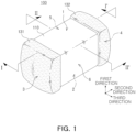
FIG. 1 is a schematic perspective view of a multilayer electronic component according to an example embodiment of the present disclosure; -
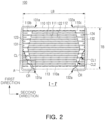
FIG. 2 is a schematic cross-sectional view taken along line I-I' ofFIG. 1 ; -
FIG. 3 is a schematic cross-sectional view taken along line II-II' ofFIG. 1 ; -
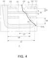
FIG. 4 is an enlarged view of region "A" ofFIG. 2 ; -
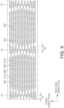
FIG. 5 is a schematic cross-sectional view of a ceramic laminate for manufacturing a multilayer electronic component illustrated inFIG. 2 ; -
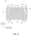
FIG. 6 is a schematic cross-sectional view of a multilayer electronic component according to another example embodiment of the present disclosure, and corresponds toFIG. 2 ; -
FIG. 7 is a schematic cross-sectional view of a ceramic laminate for manufacturing a multilayer electronic component illustrated inFIG. 6 , and corresponds toFIG. 5 ; -
FIG. 8 is a schematic cross-sectional view of a multilayer electronic component according to another example embodiment of the present disclosure, and corresponds toFIG. 2 ; -
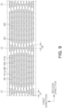
FIG. 9 is a schematic cross-sectional view of a ceramic laminate for manufacturing a multilayer electronic component illustrated inFIG. 8 , and corresponds toFIG. 5 ; and -
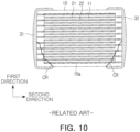
FIG. 10 is a schematic cross-sectional view of a state of a multilayer electronic component according to the related art in which a crack has occurred, and corresponds toFIG. 2 . - Hereinafter, example embodiments of the present disclosure are described with reference to the accompanying drawings. The present disclosure may, however, be exemplified in many different forms and should not be construed as being limited to the specific example embodiments set forth herein. In addition, example embodiments of the present disclosure may be provided for a more complete description of the present disclosure to those skilled in the art. Accordingly, the shapes and sizes of the elements in the drawings may be exaggerated for clarity of description, and elements denoted by the same reference numerals in the drawings may be the same elements.
- In order to clearly illustrate the present disclosure, portions not related to the description are omitted, and sizes and thicknesses are magnified in order to clearly represent layers and regions, and similar portions having the same functions within the same scope are denoted by similar reference numerals throughout the specification. Throughout the specification, when an element is referred to as "comprising" or "including," it means that it may include other elements as well, rather than excluding other elements, unless specifically stated otherwise.
- In the drawings, a first direction may be defined as a thickness (T) direction, a second direction may be defined as a length (L) direction, and a third direction may be defined as a width (W) direction.
-
-
FIG. 1 is a schematic perspective view of a multilayer electronic component according to an example embodiment of the present disclosure. -
FIG. 2 is a schematic cross-sectional view taken along line I-I' ofFIG. 1 . -
FIG. 3 is a schematic cross-sectional view taken along line II-II' ofFIG. 1 . -
FIG. 4 is an enlarged view of region "A" ofFIG. 1 . -
FIG. 5 is a schematic cross-sectional view of a ceramic laminate for manufacturing a multilayer electronic component illustrated inFIG. 2 . - Hereinafter, a multilayer
electronic component 100 according to an example embodiment of the present disclosure will be described in detail with reference toFIGS. 1 to 5 . In addition, a multilayer ceramic capacitor (hereinafter referred to as "MLCC") is described as an example of the multilayer electronic component, but the present disclosure is not limited thereto, and may be applied to various electronic products, such as inductors, piezoelectric elements, varistors, thermistors, or the like. - As used hereinafter, the expression "substantially constant length" may refer to being a same length as other lengths compared therewith, as will be appreciated by those of skill in the art, and allows for approximations, inaccuracies and limits of measurement under the relevant circumstances. In one or more aspects, the terms "substantially," "about," and "approximately" may provide an industry-accepted tolerance for their corresponding terms and/or relativity between items, such as a tolerance of ± 1%, ± 5% , or ± 10% of the actual value stated, and other suitable tolerances.
- The multilayer
electronic component 100 according to an example embodiment of the present disclosure may include abody 110 including adielectric layer 111 andinternal electrodes external electrodes - A specific shape of the
body 110 is not particularly limited. However, as illustrated, thebody 110 may have a hexahedral shape or a shape similar thereto. During a sintering process, ceramic powder particles, included in thebody 110, may shrink or an edge portion of thebody 110 may be polished, such that thebody 110 may not have a hexahedral shape having perfectly straight lines, but may have a substantially hexahedral shape. - The
body 110 may have first andsecond surfaces 1 and 2 opposing each other in the first direction, third andfourth surfaces second surfaces 1 and 2, and fifth andsixth surfaces fourth surfaces - The
body 110 may include adielectric layer 111 andinternal electrodes dielectric layer 111 in the first direction. A plurality ofdielectric layers 111, included in thebody 110, may be in a sintered state, and adjacentdielectric layers 111 may be integrated with each other such that boundaries therebetween are not readily apparent without using a scanning electron microscope (SEM). - The
dielectric layer 111 may include, for example, a perovskite-type compound, represented by ABO3, as a main component. The perovskite-type compound, represented by ABO3, may be, for example, (Ba1-xCax)TiO3 (0<x<1), Ba(Ti1-yCay)O3 (0<y<1), (Ba1-xCax)(Ti1-yZry)O3 (0<x<1, 0<y<1), or Ba (Ti1-yZry)O3 (0<y<1) obtained by partially dissolving Ca or Zr in BaTiO3. - An average thickness (td) of the
dielectric layer 111 is not particularly limited. The average thickness (td) of thedielectric layer 111 may be, for example, 0.1 to 20 µm, 0.1 to 10 µm, 0.1 to 5 µm, 0.1 to 2 µm, or 0.1 to 0.4 µm. - The
internal electrodes internal electrode 121 and a secondinternal electrode 122 alternately disposed in the first direction with thedielectric layer 111 interposed therebetween. The firstinternal electrode 121 and the secondinternal electrode 122, a pair of electrodes having different polarities, may be disposed to oppose each other with thedielectric layer 111 interposed therebetween. The firstinternal electrode 121 and the secondinternal electrode 122 may be electrically isolated from each other by thedielectric layer 111 interposed therebetween. - The first
internal electrode 121 may be spaced apart from thefourth surface 4, and may be connected to the firstexternal electrode 131 on thethird surface 3. The secondinternal electrode 122 may be spaced apart from thethird surface 3, and may be connected to the secondexternal electrode 132 on thefourth surface 4. - A conductive metal, included in the
internal electrodes - An average thickness (te) of each of the
internal electrodes internal electrodes - The average thickness (td) of the
dielectric layer 111 and the average thickness (te) of each of theinternal electrodes dielectric layer 111 in the first direction, and a size of each of theinternal electrodes dielectric layer 111 and the average size (te) of each of theinternal electrodes body 110 in the first and second directions at a magnification of 10,000. More specifically, the average thickness (td) of thedielectric layer 111 may be measured by measuring thicknesses of onedielectric layer 111 at multiple points of thedielectric layer 111, for example, thirty points equally spaced apart from each other in the second direction, and calculating an average value of the thicknesses. In addition, the average thickness (te) of each of theinternal electrodes internal electrodes internal electrodes overlapping region 110a. When such average value measurement is performed on tendielectric layers 111 and teninternal electrodes dielectric layer 111 and the average thickness (te) of each of theinternal electrodes - The
body 110 may include anoverlapping region 110a in which the firstinternal electrode 121 overlaps the secondinternal electrode 122 adjacent thereto in the first direction with thedielectric layer 111 interposed therebetween, afirst margin region 110b disposed between theoverlapping region 110a and thethird surface 3, thefirst margin region 110b in which the secondinternal electrode 122 is not disposed, and asecond margin region 110c disposed between theoverlapping region 110a and thefourth surface 4, thesecond margin region 110c in which the firstinternal electrode 121 is not disposed. - The
body 110 may include afirst cover portion 112 and asecond cover portion 113, disposed on both surfaces of theoverlapping region 110a opposing each other in the first direction. Thefirst cover portion 112 may be continuously disposed on one surface of theoverlapping region 110a in the first direction, one surface of thefirst margin region 110b in the first direction, and one surface of thesecond margin region 110c in the first direction. Thesecond cover portion 113 may be continuously disposed on the other surface of theoverlapping region 110a in the first direction, one surface of thefirst margin region 110b in the first direction, and the other surface of thesecond margin region 110c in the first direction. Thecover portions cover portions dielectric layer 111, except that an internal electrode is not included. - An average thickness of each of the
cover portions cover portions cover portions cover portions first cover portion 112 and thesecond cover portion 113. The average thickness of each of thecover portions cover portions cover portions body 110 in the first and second directions. - The
body 110 may include afirst margin portion 114 and asecond margin portion 115, disposed on both surfaces of theoverlapping region 110a opposing each other in the third direction. Thefirst margin portion 114 may be continuously disposed on one surface of theoverlapping region 110a in the third direction, one surface of thefirst margin region 110b in the third direction, and one surface of thesecond margin region 110c in the third direction. Thesecond margin portion 115 may be continuously disposed on the other surface of theoverlapping region 110a in the third direction, the other surface of thefirst margin region 110b in the third direction, and the other surface of thesecond margin region 110c in the third direction. Each of themargin portions internal electrodes body 110 in a cross-section of thebody 110 in the first and third directions. Themargin portions dielectric layer 111, except that theinternal electrodes - An average thickness of each of the
margin portions margin portions margin portions margin portions second margin portions margin portions margin portions margin portions body 110 in the first and third directions. - The
external electrodes external electrode 131 connected to the firstinternal electrode 121, the firstexternal electrode 131 disposed on thethird surface 3 and extending onto portions of the first andsecond surfaces 1 and 2, and a secondexternal electrode 132 connected to the secondinternal electrode 122, the secondexternal electrode 132 disposed on thefourth surface 4 and extending onto portions of the first andsecond surface 1 and 2. The firstexternal electrode 131 may be disposed on thethird surface 3 and extending onto a portion of each of the first surface 1, thesecond surface 2, thefifth surface 5 and thesixth surface 6, and the secondexternal electrode 132 may be disposed on thefourth surface 4 to extend to a portion of each of the first surface 1, thesecond surface 2, thefifth surface 5, and thesixth surface 6. - A type or shape of the external electrode is not particularly limited, and the external electrode may have a multilayer structure. For example, the external electrode may include a base electrode layer in contact with the
internal electrodes - The base electrode layer may be a sintered electrode including a metal and glass. The metal, included in the base electrode layer, may include Cu, Ni, Pd, Pt, Au, Ag, Pb, and/or an alloy including the same, but the present disclosure is not limited thereto. The glass, included in the base electrode layer, may include one or more oxides of Ba, Ca, Zn, Al, B, and Si, but the present disclosure is not limited thereto.
- The base electrode layer may be formed of only a first layer including a metal and glass, but the present disclosure is not limited thereto, and the base electrode layer may have a multilayer structure. For example, the base electrode layer may include a first layer including a metal and glass, and a second layer disposed on the first layer, the second layer including a metal and a resin.
- The metal, included in the second layer, may include one or more of spherical particles and flake-type particles. Here, the spherical particles may have a shape that is not completely spherical, for example, a shape in which a length ratio (long axis/short axis) between a long axis and a short axis is 1.45 or less. The flake-type particles may refer to particles having a flat and elongated shape, but the present disclosure is not particularly limited thereto. For example, the flake-type particles may have a shape in which a length ratio (long axis/short axis) between a long axis and a short axis may be 1.95 or more. The metal, included in the second layer, may include, for example, Cu, Ni, Pd, Pt, Au, Ag, Pb, Sn and/or an alloy including the same. The resin, included in the second layer, may include, for example, one or more of an epoxy resin, an acrylic resin, and ethyl cellulose.
- The plating layer may improve mounting properties. A type of the plating layer is not particularly limited, and may be a plating layer including Ni, Sn, Pd, and/or an alloy including the same, and may be formed of a plurality of layers. The plating layer may be, for example, a Ni plating layer or a Sn plating layer, or may be a Ni plating layer and a Sn plating layer, sequentially formed. In addition, the plating layer may include a plurality of Ni plating layers and/or a plurality of Sn plating layers.
- In the drawings, a structure is illustrated in which the multilayer
electronic component 100 has twoexternal electrodes external electrodes internal electrodes - When flexural stress is applied to the multilayer
electronic component 100, the stress may be concentrated onends body 110 may have a crack CR extending to the inside of thebody 110 from an end of at least one of the first and secondexternal electrodes end 131a of the first external electrode to thethird surface 3 through thefirst margin region 110b, or from anend 132a of the second external electrode to thefourth surface 4 through thesecond margin region 110c. The existence of this type of crack CR in thebody 110 may be attributed to the stress applied by theends body 110 in contact with them. A propagation path of the crack CR may vary depending on a density of a medium. For example, a slope in the second direction of at least a portion of a section CL2 of the crack CR, passing through the dielectric layer, may be steeper, based on a plane of incidence, than a slope in the second direction of a section CL1 of the crack CR, passing through the first or second internal electrode. - According to an example embodiment of the present disclosure, a length in the second direction of a central portion of the
overlapping region 110a in the first direction may be greater than that of both ends of theoverlapping region 110a in the first direction. For example, a length in the second direction of a central portion of each of themargin regions margin regions overlapping region 110a in the first direction may be greater than that of both ends of theoverlapping region 110a in the first direction, such that the crack CR may be spaced apart from the overlappingregion 110a even when the crack CR is present in thebody 110. -
FIG. 10 is a schematic cross-sectional view of a state of a multilayer electronic component according to the related art in which a crack has occurred, and corresponds toFIG. 2 . Referring toFIG. 10 , abody 10 of the multilayer electronic component according to the related art may include anoverlapping region 10a in which a firstinternal electrode 21 overlaps a secondinternal electrode 22 adjacent thereto with adielectric layer 11 interposed therebetween. However, a length of theoverlapping region 10a in the second direction may be generally constant in a central portion of theoverlapping region 10a in the first direction and both ends of theoverlapping region 10a in the first direction. - In a case according to the related art, when a crack CR propagates from ends of
external electrodes body 10, the crack CR may pass through theoverlapping region 10a, resulting in a short circuit defect. In order to resolve such an issue, a method of reducing an overall length of theoverlapping region 10a in the second direction to prevent the crack CR from extending to the inside of theoverlapping region 10a may be considered. However, as the length of theoverlapping region 10a in the second direction is reduced, a side effect of lowering capacitance and DC-bias properties of the multilayer electronic component may occur. - The multilayer
electronic component 100 according to an example embodiment of the present disclosure has a structure in which the central portion of theoverlapping region 110a in the first direction, having a longer distance from the crack CR, has a length in the second direction longer than that of both ends of theoverlapping region 110a, having a shorter distance from the crack CR, thereby preventing the crack CR from propagating to the inside of theoverlapping region 110a to prevent a short circuit defect from occurring, and improving capacitance and DC-bias properties of the multilayerelectronic component 100 as compared to a case in which an overall length of theoverlapping region 110a in the second direction is reduced. - It may be sufficient when the length in the second direction of the central portion of the
overlapping region 110a in the first direction is greater than that of both ends of theoverlapping region 110a in the first direction, and a specific shape of theoverlapping region 110a is not particularly limited. For example, a length of theoverlapping region 110a in the second direction may gradually decrease from the central portion of theoverlapping region 110a in the first direction to both ends of theoverlapping region 110a in the first direction. For example, a length in the second direction in which the firstexternal electrode 131 and the secondinternal electrode 122 are spaced apart from each other may gradually increase from the central portion of theoverlapping region 110a in the first direction to both ends of theoverlapping region 110a in the first direction, and a length in the second direction in which the secondexternal electrode 132 and the firstinternal electrode 121 are spaced apart from each other may gradually increase from the central portion of theoverlapping region 110a in the first direction to both ends of theoverlapping region 110a in the first direction. As a result, the present disclosure may have a more significant effect of improving capacitance and DC-bias properties while preventing a short circuit defect from occurring. - A distance in the second direction between the
overlapping region 110a and the crack CR may gradually increase from both ends of theoverlapping region 110a in the first direction toward the central portion of theoverlapping region 110a in the first direction, but the present disclosure is not limited thereto. - Referring to
FIGS. 2 and4 , in an example embodiment, in the cross-section of thebody 110 in the first and second directions, a distance in the second direction (LE) between the third surface and an end of the first external electrode in the second direction may be greater than a distance in the second direction (LM) between the third surface and the second internal electrode disposed on an outermost portion of thebody 110 in the first direction. That is, LE>LM may be satisfied. - The crack CR, propagating from the
ends body 110, may easily occur as high pressure is applied to the multilayerelectronic component 100. When LE is shorter than the LM in order to prevent a short circuit defect from occurring due to the crack CR from extending to the inside of theoverlapping region 110a, flexural strength of a high-pressure electronic component may not be ensured. - That is, when the crack CR, extending to the inside of the
body 110 from theends region 110a and LE>LM is satisfied, a certain or higher level of flexural strength may be ensured while preventing a short circuit from occurring in a high-pressure electronic component. - In an example embodiment, when a distance in the first direction between a crack surface having a crack on the
end 131a of the first external electrode, among the first andsecond surfaces 1 and 2, and the secondinternal electrode 122 disposed on the outermost portion of thebody 110 is denoted by TM, and an angle between a straight line CL connecting one end and the other end of the crack to each other and the crack surface is denoted by θ, LM>LE-TM×tan (90°-θ) may be satisfied. InFIGS. 3 and4 , the crack surface may be the second surface. One end of the crack CR, present on theend 131a of the first external electrode, may be positioned on the second surface, and the other end of the crack CR may be positioned on thethird surface 3. When LM>LE-TM×tan (90°-θ) is satisfied, a certain or higher level of flexural strength may be ensured while preventing a short circuit defect from occurring in a high-pressure electronic component. θ may be, for example, 60° to 70°. - When LM>LE-TM×tan (90°-θ) is satisfied, LM is not particularly limited. However, when a length of the body in the second direction is denoted by LB, a ratio (LM/LB) of LM to LB may be 0.05 to 0.4.
- In addition, TM is not particularly limited, but a thickness of the cover portion may increase as TM increases, and thus a crack CR may be less likely to occur in the multilayer
electronic component 100, and may not extend to the inside of theoverlapping region 110a even when the crack CR occurs. However, as TM increases, a volume of theoverlapping region 110a may decrease in a total volume of thebody 110, and thus the multilayerelectronic component 100 may have reduced capacitance. In the present disclosure, the length in the second direction of the central portion of theoverlapping region 110a in the first direction may be greater than that of both ends of theoverlapping region 110a in the first direction. Thus, even when a ratio (TM/TB) of TM to a thickness (TB) of thebody 110 in the first direction of thebody 110 is 0.3 or less, a certain or higher level of flexural strength and capacitance may be ensured while preventing a short circuit defect from occurring in a multilayer electronic component. A lower limit of the ratio (TM/TB) of TM to TB is not particularly limited, but may be 0.05 or more. - In an example embodiment, the
body 110 may include afirst dummy electrode 123 disposed to be spaced apart from the secondinternal electrode 122 in the second direction, thefirst dummy electrode 123 connected to the firstexternal electrode 131, and asecond dummy electrode 124 disposed to be spaced apart from the firstinternal electrode 121 in the second direction, thesecond dummy electrode 124 connected to the secondexternal electrode 132. Thefirst dummy electrode 123 may be substantially coplanar with the secondinternal electrode 122, and thesecond dummy electrode 124 may be substantially coplanar with the firstinternal electrode 121. - The
dummy electrodes body 110, such that a multilayer electronic component according to an example embodiment of the present disclosure may be manufactured without increasing a type of internal electrode pattern printed on a ceramic green sheet to be described below. - In an example embodiment, a length of the
first dummy electrode 123 in the second direction, measured in the central portion of theoverlapping region 110a in the first direction, may be shorter than a length of thefirst dummy electrode 123 in the second direction, measured in both ends of theoverlapping region 110a in the first direction. In addition, a length of thesecond dummy electrode 124 in the second direction, measured in the central portion of theoverlapping region 110a in the first direction, may be shorter than a length of thesecond dummy electrode 124 in the second direction, measured in both ends of theoverlapping region 110a in the first direction. - For example, the length of the
first dummy electrode 123 in the second direction may increase from a center of thebody 110 in the first direction toward an outer portion of thebody 110 in the first direction, and the length of thesecond dummy electrode 124 in the second direction may increase from the center of thebody 110 in the first direction toward the outer portion of thebody 110 in the first direction. - In an example embodiment, a gap between the
first dummy electrode 123 and the secondinternal electrode 122 in the second direction may be substantially constant from a topmost first dummy electrode to a bottommost first dummy electrode. Likewise, a gap between thesecond dummy electrode 124 and the firstinternal electrode 121 in the second direction may be substantially constant from a topmost second dummy electrode to a bottommost second dummy electrode. - In an example embodiment, when a distance in a second direction between the second
internal electrode 122, disposed on the outermost portion of thebody 110 in the first direction, and thefirst dummy electrode 123, disposed on the outermost portion of thebody 110 in the first direction, is denoted by LD, a ratio (LD/LM) of LD to LM may be 0.3 or more. When LD/LM is less than 0.3, the secondinternal electrode 122 and thefirst dummy electrode 123 may come into contact with each other to cause a short circuit defect. An upper limit of LD/LM is not particularly limited, but may be 0.8 or less. - Hereinafter, an example of a method of forming the multilayer
electronic component 100 according to an example embodiment of the present disclosure will be described with reference toFIG. 5 . - First, ceramic powder particles for forming ceramic
green sheets green sheets - Subsequently, the
internal electrode patterns green sheets internal electrode patterns 221 may be formed on a first ceramicgreen sheet 211a, and a plurality of secondinternal electrode patterns 222 may be formed on a second ceramicgreen sheet 211b. - Subsequently, the ceramic
green sheets internal electrode patterns green sheet 211a on which the firstinternal electrode pattern 221 is formed and the second ceramicgreen sheet 211b on which the second internal electrode pattern is formed may be alternately laminated to correspond to a predetermined number of layers and then compressed to form aceramic laminate 200 illustrated inFIG. 5 . A ceramic green sheet on which an internal electrode pattern is not formed may be laminated on upper and lower portions of theceramic laminate 200 to correspond to a predetermined number of layers to form thecover portions ceramic laminate 200 may be cut along a cutting line C1 to have a predetermined chip size, and the cut chip may be sintered at a temperature, for example, greater than or equal to 1000°C and less than or equal to 1400°C to form thebody 110. In this case, a length D1 in which an end of the first internal electrode pattern is offset with respect to the cutting line C1 increases from a central portion of theceramic laminate 200 in the first direction toward both ends of theceramic laminate 200 in the first direction. In addition, a length D2 in which an end of the second internal electrode pattern is offset with respect to the cutting line C1 increases from the central portion of theceramic laminate 200 in the first direction toward both ends of theceramic laminate 200 in the first direction. As a result, the length in the second direction of the central portion of theoverlapping region 110a in the first direction on which sintering has been performed may be greater than that of both ends of theoverlapping region 110a in the first direction. - The
margin portions internal electrodes margin portions - Thereafter, the
body 110 may be dipped in a conductive paste including metal powder particles, a glass frit, a binder, and an organic solvent, and then the conductive paste may be sintered to form a base electrode layer. When the base electrode layer includes a first layer including a metal and glass, and a second layer including a metal and a resin, the second layer may be formed on the first layer by dipping in a conductive resin composition including metal powder particles, a resin, a binder, and an organic solvent, and then performing curing heat treatment at a temperature of 250°C to 550°C. Subsequently, the multilayerelectronic component 100 may be manufactured by forming a plating layer using an electroplating method and/or an electroless plating method. - A crack CR extending from an end of the external electrode to the inside of the
body 110 may be formed by flexural stress applied to the multilayerelectronic component 100. However, the length in the second direction of the central portion of theoverlapping region 110a in the first direction may be greater than that of both ends of theoverlapping region 110a in the first direction, such that the crack CR may be spaced apart from the overlappingregion 110a. - However, the above-described manufacturing method is an example, and the method of manufacturing the multilayer
electronic component 100 is not limited to the above-described manufacturing method. -
FIG. 6 is a schematic cross-sectional view of a multilayer electronic component 100' according to another example embodiment of the present disclosure, and corresponds toFIG. 2 .FIG. 7 is a schematic cross-sectional view of a ceramic laminate 200' for manufacturing the multilayer electronic component 100' illustrated inFIG. 6 , and corresponds toFIG. 5 . - Hereinafter, a multilayer electronic component 100' and a ceramic laminate 200' for manufacturing the multilayer electronic component 100' according to another example embodiment of the present disclosure will be described with reference to
FIGS. 6 and7 . The same/similar reference numerals are used for components the same as/similar to those of the multilayerelectronic component 100 and theceramic laminate 200 illustrated inFIGS. 1 to 5 , and thus repeated descriptions will be omitted. - Referring to
FIG. 6 , a length of anoverlapping region 110a' in the second direction may decrease in a stepwise manner from a central portion of theoverlapping region 110a' in the first direction toward both ends of theoverlapping region 110a' in the first direction. - The multilayer electronic component 100' according to an example embodiment of the present disclosure may have a structure in which the length of the
overlapping region 110a' in the second direction decreases in a stepwise manner from the central portion of theoverlapping region 110a' in the first direction to both ends of theoverlapping region 110a' in the first direction, thereby preventing a crack CR from propagating to the inside of theoverlapping region 110a' to prevent a short circuit defect from occurring, and improving capacitance and DC-bias properties of the multilayer electronic component 100' as compared to a case in which an overall length of theoverlapping region 110a' in the second direction is reduced. - Referring to
FIG. 7 , in a ceramic laminate 200' for manufacturing the multilayer electronic component 100', a length D1' in which an end of a first internal electrode pattern is offset with respect to a cutting line C1 may increase in a stepwise manner from a central portion of the ceramic laminate 200' in the first direction to both ends of the ceramic laminate 200' in the first direction. In addition, a length D2' in which an end of a second internal electrode pattern is offset with respect to the cutting line C1 may increase in a stepwise manner from the central portion of the ceramic laminate 200' in the first direction to both ends of the ceramic laminate 200' in the first direction. As a result, a length of theoverlapping region 110a' in the second direction on which sintering has been performed may be formed to decrease in a stepwise manner from the central portion of theoverlapping region 110a' in the first direction to both ends of theoverlapping region 110a' in the first direction. However, the above-described manufacturing method is an example, and the method of manufacturing the multilayer electronic component 100' is not limited to the above-described manufacturing method. -
FIG. 8 is a schematic cross-sectional view of a multilayerelectronic component 100" according to another example embodiment of the present disclosure, and corresponds toFIG. 2 .FIG. 9 is a schematic cross-sectional view of aceramic laminate 200" for manufacturing the multilayerelectronic component 100" illustrated inFIG. 8 , and corresponds toFIG. 5 . - Hereinafter, a multilayer electronic component 100'' and a
ceramic laminate 200" for manufacturing the multilayerelectronic component 100" according to another example embodiment of the present disclosure will be described with reference toFIGS. 8 and9 . The same/similar reference numerals are used for components the same as/similar to those of the multilayerelectronic component 100 and theceramic laminate 200 illustrated inFIGS. 1 to 5 , and thus repeated descriptions will be omitted. - Referring to
FIG. 8 , the overlappingregion 110a" may include a first region R1 disposed in the central portion of theoverlapping region 110a'' in the first direction, the first region R1 having a substantially constant length in the second direction, and second regions R2 and R3 having a length in the second direction gradually decreasing from the first region R1 to both ends of theoverlapping region 110a'' in the first direction. Here, the first region R1, having a substantially constant length in the second direction, may mean that a length is sufficiently constant such that those skilled in the art could understood that the length is constant, and may mean that the length is the same, including a process error, positional deviation, and measurement error occurring in a manufacturing process. - The multilayer electronic component 100'' according to an example embodiment of the present disclosure may include the second regions R2 and R3 in which a length of the
overlapping region 110a" in the second direction gradually decreases toward both ends of theoverlapping region 110a" in the first direction, thereby preventing a crack CR from propagating to the inside of theoverlapping region 110a'' to prevent a short circuit defect from occurring, and improving capacitance and DC-bias properties of the multilayerelectronic component 100" as compared to a case in which an overall length of theoverlapping region 110a'' in the second direction is reduced. - Referring to
FIG. 9 , theceramic laminate 200" for manufacturing the multilayerelectronic component 100" may be designed such that it has a section where a length D1" in which an end of a first internal electrode pattern is offset with respect to a cutting line C1 gradually increases from the inside of theceramic laminate 200" in the first direction toward both ends of theceramic laminate 200" in the first direction, and a section where the length D1" in which the end of the first internal electrode pattern is offset is substantially constant in the central portion of theceramic laminate 200" in the first direction. In addition, theceramic laminate 200" for manufacturing the multilayerelectronic component 100" may be designed such that it has a section where a length D2" in which an end of a second internal electrode pattern is offset with respect to the cutting line C1 increases from the inside of theceramic laminate 200" in the first direction toward both ends of theceramic laminate 200" in the first direction, and a section where the length D2'' in which the end of the second internal electrode pattern is offset is substantially constant in the central portion of theceramic laminate 200" in the first direction. - Accordingly, the overlapping
region 110a'' may include a first region R1 disposed on the central portion of theoverlapping region 110a" in the first direction, the first region R1 having a substantially constant length in the second direction, and second regions R2 and R3 having a length in the second direction gradually decreasing from the first region R1 to both ends of theoverlapping region 110a" in the first direction. However, the above-described manufacturing method is an example, and the method of manufacturing the multilayerelectronic component 100" is not limited to the above-described manufacturing method. - While example embodiments have been illustrated and described above, it will be apparent to those skilled in the art that modifications and variations could be made without departing from the scope of the present disclosure as defined by the appended claims.
- In addition, the term "an example embodiment" used herein does not refer to the same example embodiment, and is provided to emphasize a particular feature or characteristic different from that of another example embodiment. However, example embodiments provided herein are considered to be able to be implemented by being combined in whole or in part one with one another. For example, one element described in a particular example embodiment, even if it is not described in another example embodiment, may be understood as a description related to another example embodiment, unless an opposite or contradictory description is provided therein.
- As used herein, the terms "first," "second," and the like may be used to distinguish a component from another component, and may not limit a sequence and/or an importance, or others, in relation to the components. In some cases, a first component may be referred to as a second component, and similarly, a second component may be referred to as a first component without departing from the scope of the example embodiments.
Claims (13)
- A multilayer electronic component comprising:a body having first and second surfaces opposing each other in a first direction, third and fourth surfaces opposing each other in a second direction and connected to the first and second surfaces, fifth and sixth surfaces opposing each other in a third direction and connected to the first to fourth surfaces, the body including a dielectric layer and first and second internal electrodes alternately disposed in the first direction with the dielectric layer interposed therebetween;a first external electrode connected to the first internal electrode, the first external electrode disposed on the third surface and extending onto portions of the first and second surfaces; anda second external electrode connected to the second internal electrode, the second external electrode disposed on the fourth surface and extending onto portions of the first and second surfaces,wherein the body includes an overlapping region in which the first internal electrode overlaps the second internal electrode adjacent thereto in the first direction with the dielectric layer interposed therebetween,a length in the second direction of a central portion of the overlapping region in the first direction is greater than that of both ends of the overlapping region in the first direction, andthe body has a crack extending to an inside of the body from an end of at least one of the first and second external electrodes, the crack spaced apart from the overlapping region.
- The multilayer electronic component of claim 1, whereinthe body includes a first margin region disposed between the overlapping region and the third surface and free of the second internal electrode, and a second margin region disposed between the overlapping region and the fourth surface and free of the first internal electrode, andthe crack extends from an end of the first external electrode to the third surface through the first margin region or from an end of the second external electrode to the fourth surface through the second margin region.
- The multilayer electronic component of claim 1, whereinin a cross-section of the body in the first and second directions,when a distance in the second direction between the third surface and the second internal electrode disposed on an outermost portion of the body in the first direction is denoted by LM, and a distance in the second direction between the third surface and the end of the first external electrode is denoted by LE, LE>LM is satisfied.
- The multilayer electronic component of claim 3, wherein, when a distance between a crack surface having a crack on the end of the first external electrode, among the first and second surfaces, and the second internal electrode disposed on the outermost portion of the body in the first direction is denoted by TM, and an angle between a straight line connecting one end and the other end of the crack to each other and the crack surface is denoted by θ, LM>LE-TM×tan(90°-θ) is satisfied.
- The multilayer electronic component of claim 4, wherein θ is 60° or more and 70° or less.
- The multilayer electronic component of claim 4, wherein, when a thickness of the body in the first direction is denoted by TB, a ratio of TM to TB (TM/TB) is 0.05 or more and 0.3 or less.
- The multilayer electronic component of claim 2, wherein a slope in the second direction of at least a portion of a section of the crack, passing through the dielectric layer, is steeper, based on a plane of incidence, than a slope in the second direction of a section of the crack, passing through the first or second internal electrode.
- The multilayer electronic component of claim 1, wherein the body further includes a first dummy electrode disposed to be spaced apart from the second internal electrode in the second direction and connected to the first external electrode, and a second dummy electrode disposed to be spaced apart from the first internal electrode in the second direction and connected to the second external electrode.
- The multilayer electronic component of claim 8, wherein a length of the first dummy electrode in the second direction, measured in the central portion of the overlapping region in the first direction, is less than a length of the first dummy electrode in the second direction, measured in both ends of the overlapping region in the first direction.
- The multilayer electronic component of claim 1, wherein a length of the overlapping region in the second direction gradually decreases from the central portion of the overlapping region in the first direction toward both ends of the overlapping region in the first direction.
- The multilayer electronic component of claim 10, whereina length in the second direction in which the first external electrode and the second internal electrode are spaced apart from each other gradually increases from the central portion of the overlapping region in the first direction toward both ends of the overlapping region in the first direction, anda length in the second direction in which the second external electrode and the first internal electrode are spaced apart from each other gradually increases from the central portion of the overlapping region in the first direction toward both ends of the overlapping region in the first direction.
- The multilayer electronic component of claim 1, wherein a length of the overlapping region in the second direction decreases in a stepwise manner from the central portion of the overlapping region in the first direction to both ends of the overlapping region in the first direction.
- The multilayer electronic component of claim 1, wherein the overlapping region includes a first region disposed on the central portion of the overlapping region in the first direction, the first region having a substantially constant length in the second direction, and a second region having a length in the second direction gradually decreasing from the first region to both ends of the overlapping region in the first direction.
Applications Claiming Priority (1)
| Application Number | Priority Date | Filing Date | Title |
|---|---|---|---|
| KR1020230192398A KR20250101118A (en) | 2023-12-27 | 2023-12-27 | Multilayer electronic component |
Publications (2)
| Publication Number | Publication Date |
|---|---|
| EP4579699A2 true EP4579699A2 (en) | 2025-07-02 |
| EP4579699A3 EP4579699A3 (en) | 2025-11-12 |
Family
ID=93430460
Family Applications (1)
| Application Number | Title | Priority Date | Filing Date |
|---|---|---|---|
| EP24210833.0A Pending EP4579699A3 (en) | 2023-12-27 | 2024-11-05 | Multilayer electronic component comprising a crack extending to an inside of the body from an end of one of the external electrodes |
Country Status (5)
| Country | Link |
|---|---|
| US (1) | US20250218668A1 (en) |
| EP (1) | EP4579699A3 (en) |
| JP (1) | JP2025104268A (en) |
| KR (1) | KR20250101118A (en) |
| CN (1) | CN120221281A (en) |
Family Cites Families (5)
| Publication number | Priority date | Publication date | Assignee | Title |
|---|---|---|---|---|
| JP2002299148A (en) * | 2001-03-30 | 2002-10-11 | Kyocera Corp | Multilayer ceramic capacitor and method of manufacturing the same |
| KR20150019643A (en) * | 2013-08-14 | 2015-02-25 | 삼성전기주식회사 | Multi-layered ceramic capacitor |
| KR101792385B1 (en) * | 2016-01-21 | 2017-11-01 | 삼성전기주식회사 | Multi-layered ceramic capacitor and board for mounting the same |
| KR102834093B1 (en) * | 2020-09-18 | 2025-07-15 | 삼성전기주식회사 | Mutilayer electronic component |
| KR102880989B1 (en) * | 2020-12-09 | 2025-11-04 | 삼성전기주식회사 | Mutilayer electronic component |
-
2023
- 2023-12-27 KR KR1020230192398A patent/KR20250101118A/en active Pending
-
2024
- 2024-11-05 EP EP24210833.0A patent/EP4579699A3/en active Pending
- 2024-11-18 US US18/951,524 patent/US20250218668A1/en active Pending
- 2024-11-25 JP JP2024204403A patent/JP2025104268A/en active Pending
- 2024-12-26 CN CN202411931607.1A patent/CN120221281A/en active Pending
Also Published As
| Publication number | Publication date |
|---|---|
| JP2025104268A (en) | 2025-07-09 |
| EP4579699A3 (en) | 2025-11-12 |
| CN120221281A (en) | 2025-06-27 |
| KR20250101118A (en) | 2025-07-04 |
| US20250218668A1 (en) | 2025-07-03 |
Similar Documents
| Publication | Publication Date | Title |
|---|---|---|
| US11476047B2 (en) | Multilayer electronic component | |
| US11735374B2 (en) | Multi-layered ceramic electronic component | |
| US11961673B2 (en) | Multilayer ceramic capacitor | |
| CN110942913A (en) | Ceramic Electronic Components | |
| CN116844861A (en) | Multilayer electronic components | |
| EP4542598A1 (en) | Multilayer electronic component | |
| EP4379762B1 (en) | Multilayer electronic component (mlcc) improved interface with external electrodes | |
| EP4401104A2 (en) | Multilayer electronic component | |
| US20250218668A1 (en) | Multilayer electronic component | |
| US12374496B2 (en) | Multilayer electronic component | |
| US12198860B2 (en) | Multilayer electronic component and method of manufacturing the same | |
| KR20240147249A (en) | Multilayer electronic component | |
| CN111009415A (en) | Ceramic electronic component | |
| US20250210260A1 (en) | Multilayer electronic component | |
| CN116417260A (en) | Multilayer electronic component | |
| US20250118492A1 (en) | Multilayer electronic component | |
| EP4560666A1 (en) | Multilayer electronic component | |
| US12633464B2 (en) | Multilayer electronic component | |
| US20260094769A1 (en) | Multilayer electronic component | |
| EP4579700A1 (en) | Multilayer electronic component | |
| EP4576136A1 (en) | Multilayer electronic component | |
| JP2025105544A (en) | Multilayer Electronic Components | |
| CN122000201A (en) | Multilayer electronic component | |
| JP2025040934A (en) | Multilayer Electronic Components | |
| JP2026000838A (en) | Multilayer electronic components |
Legal Events
| Date | Code | Title | Description |
|---|---|---|---|
| PUAI | Public reference made under article 153(3) epc to a published international application that has entered the european phase |
Free format text: ORIGINAL CODE: 0009012 |
|
| STAA | Information on the status of an ep patent application or granted ep patent |
Free format text: STATUS: THE APPLICATION HAS BEEN PUBLISHED |
|
| AK | Designated contracting states |
Kind code of ref document: A2 Designated state(s): AL AT BE BG CH CY CZ DE DK EE ES FI FR GB GR HR HU IE IS IT LI LT LU LV MC ME MK MT NL NO PL PT RO RS SE SI SK SM TR |
|
| PUAL | Search report despatched |
Free format text: ORIGINAL CODE: 0009013 |
|
| AK | Designated contracting states |
Kind code of ref document: A3 Designated state(s): AL AT BE BG CH CY CZ DE DK EE ES FI FR GB GR HR HU IE IS IT LI LT LU LV MC ME MK MT NL NO PL PT RO RS SE SI SK SM TR |
|
| RIC1 | Information provided on ipc code assigned before grant |
Ipc: H01G 4/008 20060101AFI20251007BHEP Ipc: H01G 4/012 20060101ALI20251007BHEP Ipc: H01G 4/12 20060101ALI20251007BHEP Ipc: H01G 4/232 20060101ALI20251007BHEP Ipc: H01G 4/30 20060101ALI20251007BHEP |
|
| STAA | Information on the status of an ep patent application or granted ep patent |
Free format text: STATUS: REQUEST FOR EXAMINATION WAS MADE |
|
| 17P | Request for examination filed |
Effective date: 20260330 |