EP4579494A2 - Verfahren, systeme, herstellungsartikel und vorrichtung zur decodierung von nullwertkompressionsdatenvektoren - Google Patents
Verfahren, systeme, herstellungsartikel und vorrichtung zur decodierung von nullwertkompressionsdatenvektoren Download PDFInfo
- Publication number
- EP4579494A2 EP4579494A2 EP25176972.5A EP25176972A EP4579494A2 EP 4579494 A2 EP4579494 A2 EP 4579494A2 EP 25176972 A EP25176972 A EP 25176972A EP 4579494 A2 EP4579494 A2 EP 4579494A2
- Authority
- EP
- European Patent Office
- Prior art keywords
- sparsity
- tensor
- data
- valued
- bitmap
- Prior art date
- Legal status (The legal status is an assumption and is not a legal conclusion. Google has not performed a legal analysis and makes no representation as to the accuracy of the status listed.)
- Pending
Links
Images








Classifications
-
- G—PHYSICS
- G06—COMPUTING OR CALCULATING; COUNTING
- G06F—ELECTRIC DIGITAL DATA PROCESSING
- G06F16/00—Information retrieval; Database structures therefor; File system structures therefor
- G06F16/20—Information retrieval; Database structures therefor; File system structures therefor of structured data, e.g. relational data
- G06F16/22—Indexing; Data structures therefor; Storage structures
- G06F16/2228—Indexing structures
- G06F16/2237—Vectors, bitmaps or matrices
-
- G—PHYSICS
- G06—COMPUTING OR CALCULATING; COUNTING
- G06F—ELECTRIC DIGITAL DATA PROCESSING
- G06F17/00—Digital computing or data processing equipment or methods, specially adapted for specific functions
- G06F17/10—Complex mathematical operations
- G06F17/15—Correlation function computation including computation of convolution operations
- G06F17/153—Multidimensional correlation or convolution
-
- G—PHYSICS
- G06—COMPUTING OR CALCULATING; COUNTING
- G06F—ELECTRIC DIGITAL DATA PROCESSING
- G06F17/00—Digital computing or data processing equipment or methods, specially adapted for specific functions
- G06F17/10—Complex mathematical operations
- G06F17/16—Matrix or vector computation, e.g. matrix-matrix or matrix-vector multiplication, matrix factorization
-
- G—PHYSICS
- G06—COMPUTING OR CALCULATING; COUNTING
- G06N—COMPUTING ARRANGEMENTS BASED ON SPECIFIC COMPUTATIONAL MODELS
- G06N3/00—Computing arrangements based on biological models
- G06N3/02—Neural networks
- G06N3/04—Architecture, e.g. interconnection topology
- G06N3/0464—Convolutional networks [CNN, ConvNet]
-
- G—PHYSICS
- G06—COMPUTING OR CALCULATING; COUNTING
- G06N—COMPUTING ARRANGEMENTS BASED ON SPECIFIC COMPUTATIONAL MODELS
- G06N3/00—Computing arrangements based on biological models
- G06N3/02—Neural networks
- G06N3/04—Architecture, e.g. interconnection topology
- G06N3/0495—Quantised networks; Sparse networks; Compressed networks
-
- G—PHYSICS
- G06—COMPUTING OR CALCULATING; COUNTING
- G06N—COMPUTING ARRANGEMENTS BASED ON SPECIFIC COMPUTATIONAL MODELS
- G06N3/00—Computing arrangements based on biological models
- G06N3/02—Neural networks
- G06N3/06—Physical realisation, i.e. hardware implementation of neural networks, neurons or parts of neurons
- G06N3/063—Physical realisation, i.e. hardware implementation of neural networks, neurons or parts of neurons using electronic means
-
- H—ELECTRICITY
- H03—ELECTRONIC CIRCUITRY
- H03M—CODING; DECODING; CODE CONVERSION IN GENERAL
- H03M7/00—Conversion of a code where information is represented by a given sequence or number of digits to a code where the same, similar or subset of information is represented by a different sequence or number of digits
- H03M7/30—Compression; Expansion; Suppression of unnecessary data, e.g. redundancy reduction
- H03M7/3059—Digital compression and data reduction techniques where the original information is represented by a subset or similar information, e.g. lossy compression
-
- H—ELECTRICITY
- H03—ELECTRONIC CIRCUITRY
- H03M—CODING; DECODING; CODE CONVERSION IN GENERAL
- H03M7/00—Conversion of a code where information is represented by a given sequence or number of digits to a code where the same, similar or subset of information is represented by a different sequence or number of digits
- H03M7/30—Compression; Expansion; Suppression of unnecessary data, e.g. redundancy reduction
- H03M7/3066—Compression; Expansion; Suppression of unnecessary data, e.g. redundancy reduction by means of a mask or a bit-map
-
- H—ELECTRICITY
- H03—ELECTRONIC CIRCUITRY
- H03M—CODING; DECODING; CODE CONVERSION IN GENERAL
- H03M7/00—Conversion of a code where information is represented by a given sequence or number of digits to a code where the same, similar or subset of information is represented by a different sequence or number of digits
- H03M7/30—Compression; Expansion; Suppression of unnecessary data, e.g. redundancy reduction
- H03M7/3082—Vector coding
-
- G—PHYSICS
- G06—COMPUTING OR CALCULATING; COUNTING
- G06N—COMPUTING ARRANGEMENTS BASED ON SPECIFIC COMPUTATIONAL MODELS
- G06N3/00—Computing arrangements based on biological models
- G06N3/02—Neural networks
- G06N3/04—Architecture, e.g. interconnection topology
-
- G—PHYSICS
- G06—COMPUTING OR CALCULATING; COUNTING
- G06N—COMPUTING ARRANGEMENTS BASED ON SPECIFIC COMPUTATIONAL MODELS
- G06N3/00—Computing arrangements based on biological models
- G06N3/02—Neural networks
- G06N3/08—Learning methods
Definitions
- This disclosure relates generally to processors, and, more particularly, to methods, systems, articles of manufacture, and apparatus to decode zero-value-compression data vectors.
- Mobile devices typically include image processing, video processing, and speech processing capabilities that are limited by size constraints, temperature management constraints, and/or power constraints.
- neural network applications, other machine learning and/or artificial intelligence applications use such image processing, video processing, and speech processing.
- Such neural network applications, other machine learning and/or artificial intelligence applications may store data in two-dimensional vectors (e.g., maps, channels, etc.).
- the two-dimensional vectors may be grouped to produce a multi-dimensional (e.g., three-dimensional, four-dimensional, etc.) volume/array, referred to as a tensor.
- Tensors, and other multi-dimensional data structures are typically stored in memory at addresses according to a particular order (e.g., corresponding to the dimensions of the multi-dimensional data structures).
- connection references e.g., attached, coupled, connected, and joined are to be construed broadly and may include intermediate members between a collection of elements and relative movement between elements unless otherwise indicated. As such, connection references do not necessarily infer that two elements are directly connected and in fixed relation to each other.
- Descriptors "first,” “second,” “third,” etc. are used herein when identifying multiple elements or components which may be referred to separately. Unless otherwise specified or understood based on their context of use, such descriptors are not intended to impute any meaning of priority, physical order or arrangement in a list, or ordering in time but are merely used as labels for referring to multiple elements or components separately for ease of understanding the disclosed examples.
- the descriptor "first” may be used to refer to an element in the detailed description, while the same element may be referred to in a claim with a different descriptor such as "second” or “third.” In such instances, it should be understood that such descriptors are used merely for ease of referencing multiple elements or components.
- Typical computing systems employ advanced image processing, computer vision, video processing, and/or speech processing algorithms to automate tasks that human vison and/or human hearing can perform.
- Computer vision, image processing, and/or video processing tasks include acquiring, processing, analyzing, and/or otherwise understanding digital images. Such tasks facilitate, in part, extraction of dimensional data from the digital images to produce numerical and/or symbolic information.
- Computer vision algorithms can use the numerical and/or symbolic information to make decisions and/or otherwise perform operations associated with three-dimensional (3-D) pose estimation, event detection, object recognition, video tracking, among others.
- AR augmented reality
- VR virtual reality
- robotics and/or other applications it is then accordingly important to perform such tasks quickly (e.g., in real time or near real time) and efficiently.
- a DNN is an artificial neural network including multiple layers.
- DNNs can include any number of hidden layers, usually more than one.
- DNNs are typically used to classify images, cluster the images by similarity (e.g., a photo search), and/or perform object recognition within the images.
- image processing or computer vision algorithms employ convolutional neural networks (CNNs).
- CNNs convolutional neural networks
- a DNN and/or a CNN can be used to identify faces, individuals, street signs, animals, etc., included in an input image.
- DNNs and/or CNNs obtain vectors (e.g., image data that is broken down from multi-dimensional arrays) that need to be stored or used in computations to perform one or more functions.
- a DNN and/or a CNN may receive multi-dimensional arrays (e.g., tensors or rows of vectors) including data corresponding to one or more images.
- the multi-dimensional arrays are represented as vectors.
- Such vectors may include thousands of elements. Each such element may include a large number of bits. A vector with 10,000 16 bit elements corresponds to 160,000 bits of information. Storing such vectors requires significant memory. However, such vectors may include large numbers of elements with a value of zero. Accordingly, some DNNs, some CNNs and/or other processing engines may break up such a vector into a zero-value-compression (ZVC) data vector and a sparsity bitmap (e.g., a bitmap vector).
- ZVC zero-value-compression
- a sparsity bitmap e.
- a zero-value-compression (ZVC) data vector is a vector that includes all non-zero elements of a vector in the same order as a sparse vector, but excludes all zero elements.
- a sparse vector is an input vector including both non-zero elements and zero elements.
- a dense vector is an input vector including all non-zero elements.
- an example sparse vector [0, 0, 5, 0, 18, 0, 4, 0] corresponds to an example ZVC data vector [5, 18, 4].
- a sparsity bitmap is a vector that includes one-bit elements identifying whether respective elements of the sparse vector are zero or non-zero.
- a sparsity bitmap may map non-zero values of a sparse vector to '1' and may map zero values of the sparse vector to '0'.
- an example sparsity bitmap may be [0, 0, 1, 0, 1, 0, 1, 0] (e.g., because the third, fifth, seventh, and eight elements of the sparse vector are non-zero).
- the combination of the ZVC data vector and the sparsity bitmap represents the sparse vector (e.g., the sparse vector could be generated/reconstructed based on the corresponding ZVC data vector and sparsity bitmap). Accordingly, a DNN and/or a CNN engine can generate/determine the sparse vector based on the corresponding ZVC data vector and sparsity bitmap without storing the sparse vector in memory.
- Storing a ZVC data vector and a sparsity bitmap in memory instead of a sparse vector saves memory and processing resources (e.g., provided there are sufficient zeros in the sparse vector(s)). For example, if each element of the above-sparse vector (e.g., [0, 0, 5, 0, 18, 0, 4, 0]) was 16 bits of information, the amount of memory required to store the sparse vector is 128 bits (e.g., 8 elements X 16 bits).
- the amount of memory required to store the corresponding ZVC data vector (e.g., [5, 18, 4]) and the sparsity bitmap (e.g., 0, 0, 1, 0, 1, 0, 1, 0]) is 64 bits (e.g., (the 3 elements of the ZVC data vector X 16 bits) + (8 elements of the sparsity bitmap X 1 bit)). Accordingly, storing the ZVC data vector and sparsity bitmap instead of a corresponding sparse vector reduces the amount of memory needed to store such vectors. Additionally, utilizing ZVC data vectors and sparsity bitmaps improves bandwidth requirements because the amount of data being delivered into a computational engine is decreased to increase the delivery speed to the computational engine.
- Machine learning accelerators handle a large amount of tensor data (e.g., data stored in multi-dimensional data structures) for performing inference tasks. Processing large amounts of tensor data requires data movement across multiple levels of a memory hierarchy (e.g., hard drives, flash storage, RAM, cache, registers, etc.) to a processing element (PE) array. Reducing data transfer and increasing (e.g., maximizing) data reuse and resource utilization can improve energy efficiency.
- a memory hierarchy e.g., hard drives, flash storage, RAM, cache, registers, etc.
- PE processing element
- Reducing data transfer and increasing (e.g., maximizing) data reuse and resource utilization can improve energy efficiency.
- Due to the nature of DNN and/or other AI engines both inputs to the DNN (sometimes referred to as input activations and/or input feature maps) and weights (sometimes referred to as trained DNN model parameters) include sparse vectors.
- input activation vectors and/or weight vectors can include a significant amount of zero elements due to rectifying operations in DNN layers.
- utilizing ZVC data vectors and sparsity bitmaps can be an effective technique to accelerate the inference and training of a DNN as well as to reduce the storage requirement for parameters (e.g. compression) for energy efficiency.
- Examples disclosed herein include an in-line sparsity-aware tensor data distribution system that decompresses ZVC data vectors for both activations and weights and distribute to a PE array.
- the in-line sparsity-aware tensor data distribution system disclosed herein maintains data in compressed data format in each PE based on a programmable schedule (e.g., a mapping between instructions (e.g., a program, an algorithm, etc.) to selected processing elements).
- Example disclosed in-line sparsity-aware tensor data distribution systems reconstruct the sparsity bitmap per tensor on the fly in PEs.
- Examples disclosed herein store compressed data (e.g., ZVC data vectors) with sparsity bitmaps through memory hierarchies from global buffers (e.g., SRAM banks) to register files in PEs without storing zero-elements.
- compressed data e.g., ZVC data vectors
- global buffers e.g., SRAM banks
- examples disclosed herein reduce data movement and improve energy efficiency of a computing device.
- the flexible tensor distribution is controlled, at least in part, by configuration descriptors, that are not dependent on the sparsity of input data but are exposed to the compiler to be configured during runtime.
- Examples disclosed herein advantageously increase local register file utilization and decrease data movement energy expenditure by storing non-zero elements as opposed to zero elements and non-zero elements.
- Examples disclosed herein advantageously reconstruct the sparsity bitmap at PEs on the fly according to the flexible tensor shapes.
- Examples disclosed herein advantageously do not require staging buffers for uncompressed data (e.g., sparse vectors). For instance, examples disclosed herein do not require movement of zero elements through an on-chip memory hierarchy.
- Examples disclosed herein advantageously provide programmable and flexible tensor data distribution capability to support different schedules in terms of convolution loop partitioning and loop blocking (e.g. weight-stationary, activation stationary, partial sum-stationary, etc.).
- Examples disclosed herein enable energy efficient DNN accelerators to improve edge inferences for one or more AI applications including imaging, video and speech applications. Examples disclosed herein improve energy efficiency, performance, and advantageously leverage transistor scaling. Examples disclosed herein enable efficient processing of sparse data to deliver improved energy efficiency for modern AI workloads.
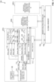
- FIG. 1 is a block diagram of an example in-line sparsity-aware tensor data distribution (InSAD) system 100.
- the InSAD system 100 includes an example first schedule-aware sparse distribution controller 102a, an example second schedule-aware sparse distribution controller 102b, an example mth schedule-aware sparse distribution controller 102m, an example memory routing controller 104, an example global memory 106, an example software compiler 108, and an example configuration description controller 110.
- Each of the example first schedule-aware sparse distribution controller 102a, the example second schedule-aware sparse distribution controller 102b, and the mth schedule-aware sparse distribution controller 102m includes any number of components.
- the structure and functionality of the example InSAD system 100 will be discussed with respect to the first schedule-aware sparse distribution controller 102a.
- the structure and functionality of the example InSAD system 100 is not limited thereto.
- the number of schedule-aware sparse distribution controllers included in the InSAD system 100 e.g., the value of m
- the first schedule-aware sparse distribution controller 102a is coupled to and/or otherwise in-circuit with the memory routing controller 104 and the configuration description controller 110.
- the example memory routing controller 104 is coupled to and/or otherwise in-circuit with the first schedule-aware sparse distribution controller 102a and the global memory 106.
- the global memory 106 is coupled to and/or otherwise in-circuit with the memory routing controller 104.
- the software compiler 108 is coupled to and/or otherwise in-circuit with the configuration description controller 110.
- the configuration description controller 110 is coupled to and/or otherwise in-circuit with the software compiler 108 and the first schedule-aware sparse distribution controller 102a.
- the first schedule-aware sparse distribution controller 102a includes an example first input buffer 112, an example first sparse decoder 114, an example first multiplexer array 116, and an example first processing element (PE) column 118.
- the example first multiplexer array 116 includes an example first multiplexer 120, an example second multiplexer 122, and an example nth multiplexer 124.
- the example first PE column 118 includes an example first PE 126, an example second PE 128, and an example nth PE 130.
- the structure and function of the example first schedule-aware sparse distribution controller 102a will be discussed with respect to input activation data.
- the structure and functionality of the example first schedule-aware sparse distribution controller 102a is not limited thereto.
- the first schedule-aware sparse distribution controller 102a can include duplicate components for input weight data.
- An example PE in accordance with such an example is discussed in connection with FIG. 3 .
- the PE array size of the platform including the InSAD system 100 is mxn, where m is the number of PE columns and n is the number of PEs in each PE column.
- the software compiler 108 generates a schedule to process data stored in the global memory 106.
- the schedule is sparsity independent.
- the software compiler 108 is implemented as a program executing on a processor.
- the software compiler 108 can be implemented by one or more analog or digital circuit(s), logic circuits, programmable processor(s), programmable controller(s), graphics processing unit(s) (GPU(s)), digital signal processor(s) (DSP(s)), application specific integrated circuit(s) (ASIC(s)), programmable logic device(s) (PLD(s)) and/or field programmable logic device(s) (FPLD(s)).
- the memory routing controller 104 controls which data is sent to which schedule-aware sparse distribution controller (e.g., the first schedule-aware sparse distribution controller 102a, the second schedule-aware sparse distribution controller 102b, the mth schedule-aware sparse distribution controller 102m, etc.).
- the memory routing controller 104 can be implemented by multiplexer array selection and/or network on chip (NOC) arbitration logic.
- NOC network on chip
- the memory routing controller 104 can be implemented by one or more analog or digital circuit(s), logic circuits, programmable processor(s), programmable controller(s), GPU(s), DSP(s), ASIC(s), PLD(s) and/or FPLD(s).
- the global memory 106 stores data on a processing platform (e.g., a mobile device, a laptop computer, a smartphone, a tablet, a workstation, etc.).
- a processing platform e.g., a mobile device, a laptop computer, a smartphone, a tablet, a workstation, etc.
- the global memory 106 can store activation data and/or weight data.
- Data stored in the global memory 106 can be stored as sparse vectors, dense vectors, ZVC data vectors, and/or sparsity bitmaps.
- the global memory 106 is implemented by SRAM and/or DRAM.
- the global memory 106 can be implemented by a volatile memory (e.g., a Synchronous Dynamic Random Access Memory (SDRAM), Dynamic Random Access Memory (DRAM), RAMBUS Dynamic Random Access Memory (RDRAM), etc.) and/or a non-volatile memory (e.g., flash memory, read only memory (ROM), programmable ROM (PROM), erasable PROM (EPROM), electrically erasable PROM (EEPROM), etc.).
- the example global memory 106 may additionally or alternatively be implemented by one or more double data rate (DDR) memories, such as DDR, DDR2, DDR3, DDR4, mobile DDR (mDDR), etc.
- DDR double data rate
- the example global memory 106 can be implemented by one or more mass storage devices such as hard disk drive(s), compact disk drive(s), digital versatile disk drive(s), solid-state disk drive(s), etc. While in the illustrated example the global memory 106 is illustrated as a single database, the global memory 106 may be implemented by any number and/or type(s) of databases. Furthermore, the data stored at the global memory 106 may be in any data format such as, for example, binary data, comma delimited data, tab delimited data, structured query language (SQL) structures, etc. In FIG. 1 , the example global memory 106 is an organized collection of data, stored on a computational system that is electronically accessible. For example, the global memory 106 may be stored on a server, a desktop computer, an HDD, an SSD, or any other suitable computing system.
- the global memory 106 may be stored on a server, a desktop computer, an HDD, an SSD, or any other suitable computing system.
- the configuration description controller 110 generates byte select signals (e.g., Byte_Sel[0] through Byte_Sel[N]) based on the schedule generated by the software compiler 108.
- the byte select signals (e.g., Byte_Sel[0] through Byte_Sel[N]) determine the shape of the tensor (e.g., two by two by three, etc.) to be processed and the volume processed by each PE according to a schedule.
- the configuration description controller 110 includes configuration descriptors that are dependent on the software programming schedule which is sparsity independent.
- the example of FIG. 2 illustrates the micro-architecture of the first sparse decoder 114 (e.g., the first flexible sparse decoder).
- the example first sparse decoder 114 obtains software programmed byte select signals (e.g. Byte_Sel[0]-Byte_Sel[7]) for each PE in a column as input.
- the example first sparse decoder 114 synchronizes the decoding operation of the sparsity bitmap. Examples disclosed herein assume the scheduling of the data distribution is identical between different PE columns. However, examples disclosed herein do not preclude other data distribution techniques.
- Each byte select signal determines the tensor shape and volume processed by each PE according to a schedule, which is sparsity independent.
- the example buffer monitor 208 implements an example means for monitoring.
- the example monitoring means is structure, and is implemented by executable instructions such as that implemented by at least blocks 1202, 1204, 1210, 1212, 1226, and 1246 of FIG. 12 .
- the executable instructions of blocks 1202, 1204, 1210, 1212, 1226, and 1246 of FIG. 12 may be executed on at least one processor such as the example processor 1512 shown in the example of FIG. 15 .
- the monitoring means is implemented by hardware logic, hardware implemented state machines, logic circuitry, and/or any other combination of hardware, software, and/or firmware.
- the data controller 210 is coupled to the configuration description controller 110 and the first multiplexer array 116.
- the data controller 210 provides (a) the first multiplexer 120 with the first sparse byte select signal (e.g., Sparse_Byte_Sel[0]), (b) the second multiplexer 122 with the second sparse byte select signal (e.g., Sparse_Byte_Sel[1]), and (c) the eighth multiplexer 124 with the eighth sparse select signal (e.g., Sparse_Byte_Sel[7]).
- the first multiplexer 120 with the first sparse byte select signal
- the second multiplexer 122 with the second sparse byte select signal
- the eighth multiplexer 124 with the eighth sparse select signal
- the data controller 210 can be implemented by one or more analog or digital circuit(s), logic circuits, programmable processor(s), programmable controller(s), GPU(s), DSP(s), application specific integrated circuit(s) ASIC(s), PLD(s) and/or FPLD(s).
- the data controller 210 generates the sparse byte select signals (e.g., Sparse_Byte_Sel[0]-Sparse_Byte_Sel[7]) based on the byte select signals (Byte_Sel[0]-Byte_Sel[7]) and/or the sparsity bitmap (e.g., the sparsity bitmap 204).
- Popcount[SB(byte_sel_i, 0)] is a sum of 1's in a sub-vector of the sparsity bitmap (SB) from the bit position of the byte select signal (e.g., byte_sel_i) to bit position 0.
- the sparse byte signals e.g. Sparse_Byte_Sel[0]-Sparse_Byte_Sel[7]
- the portion of the data from the first input buffer 112 corresponds to 16-bytes of data.
- subtracting one ensures that the data controller 210 generates the correct value for the sparse byte select signal. For example, if it is desirable for the data controller 210 to select a fifth element of data in the first input buffer 112 (e.g., the data at the fifth multiplexer (not shown)), then the sparse byte select signal should be adjusted from five to four which is [1 0 0] in binary. In such an example, this is because the first data element is chosen with zero (e.g., [0 0 0] in binary) as the sparse byte select signal.
- the data controller 210 implements example means for controlling data.
- the data controlling means is structure, and is implemented by executable instructions, such as those implemented by at least block 1238 of FIG. 12 and/or at least blocks 1306, 1308, and 1310 of FIG. 13 .
- the executable instructions of block 1238 of FIG. 12 and/or at least blocks 1306, 1308, and 1310 of FIG. 13 may be executed on at least one processor such as the example processor 1512 shown in the example of FIG. 15 .
- the data controlling means is implemented by hardware logic, hardware implemented state machines, logic circuitry, and/or any other combination of hardware, software, and/or firmware.
- the write controller 212 is coupled to the configuration description controller 110 and the first PE column 118.
- the write controller 212 provides (a) the first PE 126 with the first write enable signal (e.g., Write_en[0]), (b) the second PE 128 with the second write enable signal (e.g., Write_en[1]), and (c) the eighth PE 130 with the eighth write enable signal (e.g., Write_en[7]).
- the first PE 126 with the first write enable signal
- the second PE 128 with the second write enable signal
- the eighth PE 130 with the eighth write enable signal
- the write controller 212 can be implemented by one or more analog or digital circuit(s), logic circuits, programmable processor(s), programmable controller(s), GPU(s), DSP(s), application specific integrated circuit(s) ASIC(s), PLD(s) and/or FPLD(s).
- SB(byte_sel_i) is the value of the sparsity bitmap (e.g., the sparsity bitmap 204) at the binary bit position corresponding to the value of the byte select signal (e.g., byte_sel_i).
- the write enable signals e.g. Write _en[0]-Write_en[7] indicate whether the data transmitted to a given PE is non-zero (valid, 1, etc.) or zero (invalid, 0, etc.).
- the buffer monitor 208 additionally determines whether the header (e.g., the header 202) indicates that the data following the header is compressed data. In response to the header indicating that the data following the header include a sparsity bitmap and compressed data (e.g., the header 202 ⁇ 0xff), the buffer monitor 208 reads the sparsity bitmap (e.g., the sparsity bitmap 204) from the first input buffer 112.
- sparsity bitmaps e.g., the sparsity bitmap 204 include 16 bytes. In additional or alternative examples, sparsity bitmaps can include any number of bits.
- the first sparse decoder 114 then decodes a portion of the sparsity bitmap (e.g., the sparsity bitmap 204) that corresponds to the first portion of the ZVC data vector (e.g., the ZVC data vector 206) and a first set of byte select signals (e.g., Byte_Sel[O]-Byte_Sel[N]).
- the write controller 212 determines the value of a bit at a position in the sparsity bitmap (e.g., the sparsity bitmap 204) corresponding to the value of the byte select signal for a given PE (e.g., Byte_Sel[0] for the first PE 126).
- the write controller 212 sets the write enable signal for the given PE (e.g., Write_en[0]) equal to the value of the bit at the position in the sparsity bitmap corresponding to the byte select signal value (e.g., Byte_Sel[0]).
- the data controller 210 also sums the values of the bits between (a) the position in the sparsity bitmap (e.g., the sparsity bitmap 204) corresponding to the value of the byte select signal for a given PE (e.g., Byte_Sel[0] for the first PE 126) and (b) the LSB of the sparsity bitmap (e.g., the sparsity bitmap 204) and sets the sparse byte select signal for the given PE (e.g., Sparse_Byte_Sel[0] for the first PE 126) equal to the summed value minus one.
- the sparsity bitmap e.g., the sparsity bitmap 204
- the LSB of the sparsity bitmap e.g., the sparsity bitmap 204
- the write controller 212 will set the fourth write enable signal (e.g., Write_en[3]) to 1 (e.g., corresponding to the ninth bit position of the portion of the sparsity bitmap 204). Additionally, in such an example, the data controller 210 will set the fourth sparse byte select signal (e.g., Sparse_Byte_Sel[3]) to 4.
- the value of the fourth sparse byte select signal (e.g., Sparse_Byte_Sel[3]) for the fourth PE corresponds to the fourth byte position in the compressed data read by the first multiplexer array 116.
- the fourth multiplexer (not shown) transmits the fourth byte in the 16-byte portion of the ZVC data vector (e.g., the ZVC data vector 206).
- the fourth PE (not shown) will receive and process the fourth byte of data in the 16-byte portion of the ZVC data vector (e.g., the ZVC data vector 206) read by the first multiplexer array 116.
- Detailed operation of an example PE in accordance with the teachings of this disclosure is described in connection with FIG. 3 .
- the write controller 212, the data controller 210, and/or, more generally, the first sparse decoder 114 decodes the next portion of the sparsity bitmap corresponding to the portion of the ZVC data vector and the next byte select signal of the current set.
- the buffer monitor 208 determines whether there are any additional portions of the ZVC data vector in the first input buffer 112. If there are no additional portions of the ZVC data vector in the first input buffer 112, the buffer monitor 208 monitors the first input buffer 112.
- the pointer controller 214 In response to determining that there are additional portions of the ZVC data vector in the first input buffer 112, the pointer controller 214 translates the pointer of the first sparse decoder 114 the number of bits equal to the first portion of the sparsity bitmap (e.g., 16 bits). Subsequently, the write controller 212, the data controller 210, and/or, more generally, the first sparse decoder 114 reads an additional set of byte select signals from the configuration description controller 110. In example operation, the pointer controller 214 translates the pointer of the first multiplexer array 116 a number of bits equal to the portion of the ZVC data vector.
- the write controller 212 sets the write enable signal for a given PE (e.g., Write_en[0] for the first PE 126) equal to one.
- the data controller 210 sets the sparse byte select signal for the given PE (e.g., Sparse_Byte_Sel[0] for the first PE 126) equal to the byte select signal for the given PE (e.g., Byte_Sel[0]).
- the first multiplexer 120 transmits the data in the 16-byte portion of the uncompressed data to the first PE 126. If there are additional byte select signals in the first set of byte select signals that have not been processed, the example write controller 212 sets the write enable signal for the additional PE (e.g., Write_en[1] for the second PE 128) equal to one.
- the respective PEs e.g., the first PE 126, the second PE 128, the eighth PE 130, etc.
- the respective PEs e.g., the first PE 126, the second PE 128, the eighth PE 130, etc.
- FIG. 3 Detailed operation of an example PE in accordance with the teachings of this disclosure is described in connection with FIG. 3 .
- the byte select signals 802 include values for a first PE, PE0, a second PE, PE1, a third PE, PE2, and a fourth PE, PE3.
- the first sparse decoder 114 proceeds to the sparse byte select state 808.
- the data controller 210 determines (e.g., in a manner consistent with example Function (A)) the sparse byte select signals for the four multiplexers of the four PEs with the portion [0 1 1 1 1 0 1 0 0 0 0 0 1 1 0 1 1] of the sparsity bitmap where the right most bit is the LSB.
- the first PE, PE0 receives the first byte, 0x0a.
- FIG. 1 For the example ZVC data vector 809 of [1a 09 08 07 06 05 04 03 02 01 Of 0e 0d 0c 0b 0a], the first PE, PE0, receives the first byte, 0x0a.
- the second PE PE1
- the second PE PE1
- Sparse_Byte_Sel[2] 1, the sum of the bits between the second bit and the first bit minus one.
- the third PE, PE2 receives the second byte, 0x0b.
- the data controller 210 generate
- the first sparse decoder 114 proceeds to execute the pointer translation state 812.
- the pointer controller 214 translates the pointer of the first sparse decoder 114 and the pointer of the first multiplexer array 116.
- the pointer controller 214 translates the pointer of the first multiplexer array 116.
- the pointer controller 214 translates the pointer of the first multiplexer array 116 a first portion in the ZVC data vector 809.
- the data is invalid (as the sparsity bitmap index for the byte position is 0).
- the bit for that byte in the bitmap will be set to false (e.g., 0). In this manner, only the compressed values are loaded within a given PE.
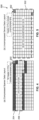
- FIG. 9 is an example graphical illustration 900 showing multiple communication schemes 902 of uncompressed dense data in accordance with the teachings of this disclosure.
- the example of FIG. 9 illustrates flexible tensor data distribution in accordance with the example in-line sparsity-aware tensor data distribution (InSAD) system 100 disclosed herein.
- the example of FIG. 9 illustrates the dense data case (no zeros in the tensor volume), where different shading patterns show the different points in this tensor.
- the example of FIG. 9 illustrates four processing elements (PEs) (e.g.
- FIG. 9 illustrates a use case of the InSAD system 100 for five different schedules with different byte select signals.
- the example of FIG. 9 illustrates the dense data case (e.g., no zeros in the tensor volume, all bytes of the tensors are filled), where different shading patterns show the different points in this tensor.
- the multiple communication schemes 902 illustrate dense data distribution for five different programmed byte select signal values.
- communication schemes 1-3 illustrate unicast cases in which each PE has different data points.
- Example scheme 4 illustrates a broadcast case in which all four PEs receive the same tensor data (e.g. same activations but different weights, where activations can be broadcasted).
- Example scheme 5 illustrates a multicast case in which some PEs receive the same tensor data.
- the disclosed InSAD system 100 is flexible and handles multiple tensor shapes for dense uncompressed data.
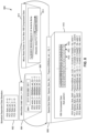
- FIG. 10 is a graphical illustration 1000 showing multiple communication schemes 1002 of zero-value-compression (ZVC) of sparse data (e.g., the original uncompressed 16 bytes) in accordance with the teachings of this disclosure.
- FIG. 10 illustrates flexible tensor data distribution in accordance with the example in-line sparsity-aware tensor data distribution (InSAD) system 100.
- PEs processing elements
- the InSAD system 100 disclosed herein supports flexible tensor distribution by programing the byte select signals according to the scheduling information for a given DNN layer.
- the graphical illustration 1000 illustrates a use case of the InSAD system 100 for five different schedules with different byte select signals.
- the example of FIG. 10 illustrates the sparse data case with ZVC, where the zero data is shown as empty blocks.
- the disclosed InSAD system 100 is flexible and handles multiple tensor shapes for ZVC data.
- FIGS. 9 and 10 illustrate five example distribution schemes including (1) unicast data of different tensor shapes (scheme 1-3), (2) broadcast data (scheme 4), and (3) multicast data (scheme 5). Because the byte select signals programmed by the configuration descriptors of the configuration description controller 110 are unaware of the sparsity in the data, the values of the byte select signals are the same between dense and sparse data, but different for different distribution schemes. As such, the disclosed InSAD system 100 is flexible and handles multiple tensor shapes and multiple data distribution schemes for uncompressed data and ZVC data.
- FIG. 11 is an example graphical illustration 1100 showing the area consumption of the in-line sparsity-aware tensor data distribution (InSAD) system 100 in accordance with the teachings of this disclosure.
- the graphical illustration 1100 illustrates the area cost of the InSAD system 100.
- the InSAD system 100 can be implemented in an SRAM buffer and load/store state machine of a processing platform.
- the input buffers occupy 2.5 kilobytes (kB) for activation and weights, respectively.
- the registers per PE occupy 384 bytes and the PEs occupy 96KB for 256 PEs.
- the input buffers and sparse decoders for both activations and weights consume 2.96% and 1% of total area of the InSAD system 100, respectively.
- Other control logic consumes 3.19% of the total area of the InSAD system 100.
- the input buffer entries can be further reduced based on the memory latency.
- the overall design overhead e.g., the input buffers, the sparse decoders, and the other control logic is only 7.15% leaving 92.85% for the overall accelerator.
- the example InSAD system 100 disclosed herein is a low-cost (3.96% area of the total PE array without SRAM area included) programmable hardware solution which can enable schedule dependent compressed data distribution in the DNN accelerators.
- the disclosed InSAD system 100 advantageously (1) does not require additional storage to hold uncompressed data during the tensor data distribution and (2) supports sparsity bitmap reconstruction for each PE during the load phase. Additionally, when implementing the disclosed InSAD system 100, programming of the byte select signals does not have sparsity dependency. Instead when implementing the disclosed InSAD system 100, programming of the byte select signals depends on the tensor shape provided by the compiler.
- the disclosed InSAD system 100 supports different tensor shapes to be processed in each PE. Because no zero data is written through the memory hierarchy during load, the data movement energy is significantly reduced with sparsity.
- FIGS. 2-11 While an example manner of implementing the in-line sparsity-aware tensor data distribution (InSAD) system 100 of FIGS. 1 is illustrated in FIGS. 2-11 and example manner of implementing ones of the first processing element (PE) 126, the second PE 128, and the nth PE 130 is illustrated in FIG. 3 as the example PE 300, one or more of the elements, processes and/or devices illustrated in FIGS. 2-11 may be combined, divided, re-arranged, omitted, eliminated and/or implemented in any other way.
- InSAD in-line sparsity-aware tensor data distribution
- the example buffer monitor 208 the example data controller 210, the example write controller 212, the example pointer controller 214, and/or, more generally, the example first sparse decoder 114, and/or the example activation transmission gate 302, the example activation register 304, the example activation sparsity bitmap register 306, the example weight transmission gate 308, the example weight register 310, the example weight sparsity bitmap register 312, the example logic processor 314, the example partial sum register 316, the example multiplier 318, the example adder 320, and/or, more generally, the example PE 300 may be implemented by hardware, software, firmware and/or any combination of hardware, software and/or firmware.
- the example PE 300 could be implemented by one or more analog or digital circuit(s), logic circuits, programmable processor(s), programmable controller(s), graphics processing unit(s) (GPU(s)), digital signal processor(s) (DSP(s)), application specific integrated circuit(s) (ASIC(s)), programmable logic device(s) (PLD(s)) and/or field programmable logic device(s) (FPLD(s)).
- the example buffer monitor 208 the example data controller 210, the example write controller 212, the example pointer controller 214, and/or, more generally, the example first sparse decoder 114, and/or the example activation transmission gate 302, the example activation register 304, the example activation sparsity bitmap 306, the example weight transmission gate 308, the example weight register 310, the example weight sparsity bitmap 312, the example logic processor 314, the example partial sum register 316, the example multiplier 318, the example adder 320, and/or, more generally, the example PE 300 is/are hereby expressly defined to include a non-transitory computer readable storage device or storage disk such as a memory, a digital versatile disk (DVD), a compact disk (CD), a Blu-ray disk, etc.
- DVD digital versatile disk
- CD compact disk
- Blu-ray disk etc.
- the example InSAD system 100, the example first sparse decoder 114, and/or the example PE 300 of FIG. 1 , FIG. 2 , and/or FIG. 3 may include one or more elements, processes and/or devices in addition to, or instead of, those illustrated in FIGS. 1-11 , and/or may include more than one of any or all of the illustrated elements, processes and devices.
- the phrase "in communication,” including variations thereof, encompasses direct communication and/or indirect communication through one or more intermediary components, and does not require direct physical (e.g., wired) communication and/or constant communication, but rather additionally includes selective communication at periodic intervals, scheduled intervals, aperiodic intervals, and/or one-time events.
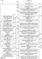
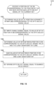
- FIGS. 12 , 13 , and 14 Flowcharts representative of example hardware logic, machine-readable instructions, hardware implemented state machines, and/or any combination thereof for implementing the example InSAD system 100 of FIG. 1 , the example first sparse decoder 114, and the example PE 300 are shown in FIGS. 12 , 13 , and 14 .
- the machine-readable instructions may be one or more executable programs or portion(s) of an executable program for execution by a computer processor such as the processor 1512 shown in the example processor platform 1500 discussed below in connection with FIG. 15 .
- the program may be embodied in software stored on a non-transitory computer readable storage medium such as a CD-ROM, a floppy disk, a hard drive, a DVD, a Blu-ray disk, or a memory associated with the processor 1512, but the entire program and/or parts thereof could alternatively be executed by a device other than the processor 1512 and/or embodied in firmware or dedicated hardware.
- a non-transitory computer readable storage medium such as a CD-ROM, a floppy disk, a hard drive, a DVD, a Blu-ray disk, or a memory associated with the processor 1512, but the entire program and/or parts thereof could alternatively be executed by a device other than the processor 1512 and/or embodied in firmware or dedicated hardware.
- the example program is described with reference to the flowcharts illustrated in FIGS. 12 , 13 , and 14 , many other methods of implementing the example InSAD system 100, the example first sparse decoder 114, and/or the example
- any or all of the blocks may be implemented by one or more hardware circuits (e.g., discrete and/or integrated analog and/or digital circuitry, an FPGA, an ASIC, a comparator, an operational-amplifier (op-amp), a logic circuit, etc.) structured to perform the corresponding operation without executing software or firmware.
- hardware circuits e.g., discrete and/or integrated analog and/or digital circuitry, an FPGA, an ASIC, a comparator, an operational-amplifier (op-amp), a logic circuit, etc.
- the machine-readable instructions described herein may be stored in one or more of a compressed format, an encrypted format, a fragmented format, a compiled format, an executable format, a packaged format, etc.
- Machine-readable instructions as described herein may be stored as data (e.g., portions of instructions, code, representations of code, etc.) that may be utilized to create, manufacture, and/or produce machine executable instructions.
- the machine-readable instructions may be fragmented and stored on one or more storage devices and/or computing devices (e.g., servers).
- the machine-readable instructions may require one or more of installation, modification, adaptation, updating, combining, supplementing, configuring, decryption, decompression, unpacking, distribution, reassignment, compilation, etc.
- the machine-readable instructions may be stored in multiple parts, which are individually compressed, encrypted, and stored on separate computing devices, wherein the parts when decrypted, decompressed, and combined form a set of executable instructions that implement a program such as that described herein.
- the machine-readable instructions may be stored in a state in which they may be read by a computer, but require addition of a library (e.g., a dynamic link library (DLL)), a software development kit (SDK), an application programming interface (API), etc. in order to execute the instructions on a particular computing device or other device.
- a library e.g., a dynamic link library (DLL)
- SDK software development kit
- API application programming interface
- the machine-readable instructions may need to be configured (e.g., settings stored, data input, network addresses recorded, etc.) before the machine-readable instructions and/or the corresponding program(s) can be executed in whole or in part.
- the disclosed machine-readable instructions and/or corresponding program(s) are intended to encompass such machine-readable instructions and/or program(s) regardless of the particular format or state of the machine-readable instructions and/or program(s) when stored or otherwise at rest or in transit.
- the machine-readable instructions described herein can be represented by any past, present, or future instruction language, scripting language, programming language, etc.
- the machine-readable instructions may be represented using any of the following languages: C, C++, Java, C#, Perl, Python, JavaScript, HyperText Markup Language (HTML), Structured Query Language (SQL), Swift, etc.
- FIGS. 12 , 13 , and 14 may be implemented using executable instructions (e.g., computer and/or machine-readable instructions) stored on a non-transitory computer and/or machine-readable medium such as a hard disk drive, a flash memory, a read-only memory, a compact disk, a digital versatile disk, a cache, a random-access memory and/or any other storage device or storage disk in which information is stored for any duration (e.g., for extended time periods, permanently, for brief instances, for temporarily buffering, and/or for caching of the information).
- a non-transitory computer readable medium is expressly defined to include any type of computer readable storage device and/or storage disk and to exclude propagating signals and to exclude transmission media.
- A, B, and/or C refers to any combination or subset of A, B, C such as (1) A alone, (2) B alone, (3) C alone, (4) A with B, (5) A with C, (6) B with C, and (7) A with B and with C.
- the phrase "at least one of A and B" is intended to refer to implementations including any of (1) at least one A, (2) at least one B, and (3) at least one A and at least one B.
- the phrase "at least one of A or B" is intended to refer to implementations including any of (1) at least one A, (2) at least one B, and (3) at least one A and at least one B.
- the phrase "at least one of A and B" is intended to refer to implementations including any of (1) at least one A, (2) at least one B, and (3) at least one A and at least one B.
- the process 1200 proceeds to block 1202. If there are additional portions of the dense vector in the first input buffer 112 (block 1246: YES), the process 1200 proceeds to block 1248.
- the first sparse decoder 114 reads an additional set of byte select signals from the configuration description controller 110 (e.g., the CDC).
- the first sparse decoder 114 translates the pointer of the first multiplexer array 116 a number of bits in the input buffer equal to the portion of the dense vector.
- the PE 300 stores the activation data in the activation register 304.
- the activation register 304 stores the activation data.
- the PE 300 translates the pointer of the activation register 304 one byte.
- the activation register 304 translates the pointer of the activation register 304 one byte.
- the PE 300 obtains weight data.
- the weight transmission gate 308 obtains weight data.
- the PE 300 obtains a weight write enable bit.
- the weight transmission gate 308 obtains a weight write enable bit.
- the PE 300 determines whether the weight write enable bit equals one (e.g., is valid). For example, at block 1416, the weight transmission gate 308 determines whether the weight write enable bit equals one. In response to the weight write enable bit not being equal to one (block 1416: NO), the process 1222 and/or the process 1242 proceeds to block 1402 and/or block 1412. In response to the weight write enable bit being equal to one (block 1416: YES), the process 1222 and/or the process 1242 proceeds to block 1418.
- the PE 300 stores the weight data in the weight register 310.
- the weight register 310 stores the weight data.
- the PE 300 translates the pointer of the weight register 310 one byte.
- the weight register 310 translates the pointer of the weight register 310 one byte.
- the logic processor 314, and/or, more generally, the PE 300 reads the data in the activation register 304.
- the multiplier 318 reads the data in the activation register 304.
- the logic processor 314, and/or, more generally, the PE 300 reads the data in the weight register 310.
- the multiplier 318 reads the data in the weight register 310.
- the PE 300 executes the multiply and accumulate operation on the data stored in the activation register 304 and/or the weight register 310.
- the logic processor 314 executes the multiply and accumulate operation on the data stored in the activation register 304 and/or the weight register 310.
- the PE 300 writes the result of the multiply and accumulate operation to the partial sum register 316.
- the adder 320 writes the result of the multiply and accumulate operation to the partial sum register 316.
- the process 1222 and/or the process 1242 return to the process 1200 at block 1224 and block 1244, respectively.
- FIG. 15 is a block diagram of an example processor platform 1500 structured to execute the instructions of FIGS. 12 , 13 , and 14 to implement the example in-line sparsity-aware tensor data distribution (InSAD) system 100 of FIG. 1 , the first sparse decoder 114 of FIG. 2 , and/or the PE 300 of FIG. 3 .
- InSAD in-line sparsity-aware tensor data distribution
- the processor platform 1500 can be, for example, a server, a personal computer, a workstation, a self-learning machine (e.g., a neural network), a mobile device (e.g., a cell phone, a smart phone, a tablet such as an iPad TM ), a personal digital assistant (PDA), an Internet appliance, a DVD player, a CD player, a digital video recorder, a Blu-ray player, a gaming console, a personal video recorder, a set top box, a headset or other wearable device, or any other type of computing device.
- a self-learning machine e.g., a neural network
- a mobile device e.g., a cell phone, a smart phone, a tablet such as an iPad TM
- PDA personal digital assistant
- an Internet appliance e.g., a DVD player, a CD player, a digital video recorder, a Blu-ray player, a gaming console, a personal video recorder, a set top box,
- the processor platform 1500 of the illustrated example includes a processor 1512.
- the processor 1512 of the illustrated example is hardware.
- the processor 1512 can be implemented by one or more integrated circuits, logic circuits, microprocessors, GPUs, DSPs, or controllers from any desired family or manufacturer.
- the hardware processor 1512 may be a semiconductor based (e.g., silicon based) device.
- the processor 1512 implements the example first schedule-aware sparse distribution controller 102a, the example second schedule-aware sparse distribution controller 102b, the example mth schedule-aware sparse distribution controller 102m, the example memory routing controller 104, the example global memory 106, the example software compiler 108, the example configuration description controller 110, the example first input buffer 112, the example first sparse decoder 114, the example first multiplexer array 116, the example first PE column 118, the example first multiplexer 120, the example second multiplexer 122, the example nth multiplexer 124, the example first PE 126, the example second PE 128, the example nth PE 130, and/or, more generally, the example InSAD system 100 of FIG.
- the example buffer monitor 208 the example data controller 210, the example write controller 212, the example pointer controller 214, and/or, more generally, the example first sparse decoder 114, and/or the example activation transmission gate 302, the example activation register 304, the example activation sparsity bitmap register 306, the example weight transmission gate 308, the example weight register 310, the example weight sparsity bitmap register 312, the example logic processor 314, the example partial sum register 316, the example multiplier 318, the example adder 320, and/or, more generally, the example PE 300.
- the processor 1512 of the illustrated example includes a local memory 1513 (e.g., a cache).
- the processor 1512 of the illustrated example is in communication with a main memory including a volatile memory 1514 and a non-volatile memory 1516 via a bus 1518.
- the volatile memory 1514 may be implemented by Synchronous Dynamic Random Access Memory (SDRAM), Dynamic Random Access Memory (DRAM), RAMBUS ® Dynamic Random Access Memory (RDRAM ® ) and/or any other type of random access memory device.
- the non-volatile memory 1516 may be implemented by flash memory and/or any other desired type of memory device. Access to the main memory 1514, 1516 is controlled by a memory controller.
- the processor platform 1500 of the illustrated example also includes an interface circuit 1520.
- the interface circuit 1520 may be implemented by any type of interface standard, such as an Ethernet interface, a universal serial bus (USB), a Bluetooth ® interface, a near field communication (NFC) interface, and/or a PCI express interface.
- one or more input devices 1522 are connected to the interface circuit 1520.
- the input device(s) 1522 permit(s) a user to enter data and/or commands into the processor 1512.
- the input device(s) can be implemented by, for example, an audio sensor, a microphone, a camera (still or video), a keyboard, a button, a mouse, a touchscreen, a track-pad, a trackball, isopoint and/or a voice recognition system.
- the interface circuit 1520 of the illustrated example also includes a communication device such as a transmitter, a receiver, a transceiver, a modem, a residential gateway, a wireless access point, and/or a network interface to facilitate exchange of data with external machines (e.g., computing devices of any kind) via a network 1526.
- the communication can be via, for example, an Ethernet connection, a digital subscriber line (DSL) connection, a telephone line connection, a coaxial cable system, a satellite system, a line-of-site wireless system, a cellular telephone system, etc.
- DSL digital subscriber line
- the processor platform 1500 of the illustrated example also includes one or more mass storage devices 1528 for storing software and/or data.
- mass storage devices 1528 include floppy disk drives, hard drive disks, compact disk drives, Blu-ray disk drives, redundant array of independent disks (RAID) systems, and digital versatile disk (DVD) drives.
- the machine executable instructions 1532 of FIGS. 12 , 13 , and 14 may be stored in the mass storage device 1528, in the volatile memory 1514, in the non-volatile memory 1516, and/or on a removable non-transitory computer readable storage medium such as a CD or DVD.
- example methods, apparatus and articles of manufacture have been disclosed that decode zero-value-compression data vectors in machine learning accelerators.
- Examples disclosed herein advantageously do not require staging buffers for uncompressed data (e.g., sparse vectors).
- Examples disclosed herein do not require movement of zero elements through on-chip memory hierarchy.
- the disclosed methods, apparatus, and articles of manufacture advantageously increase local register file utilization and decrease data movement energy consumption by storing non-zero elements as opposed to zero elements and non-zero elements.
- example disclosed methods, apparatus, and articles of manufacture reconstruct the sparsity bitmap at PEs on the fly according to the flexible tensor shapes.
- disclosed methods, apparatus, and articles of manufacture regenerate the sparsity bitmap at each PE based on its distributed tensor volume.
- examples disclosed herein support flexible tensor distribution by programing the byte select signals according to the scheduling information for a given DNN layer.
- Disclosed methods, apparatus, and articles of manufacture provide programmable flexible tensor data distribution capability to support different schedules in terms of convolution loop partitioning and loop blocking (e.g. weight-stationary, activation stationary, partial sum-stationary, etc.).
- Disclosed methods, apparatus and articles of manufacture improve the efficiency of using a computing device by reducing on-chip storage overhead for decompressed data after sparsity decoding.
- Disclosed methods, apparatus, and articles of manufacture advantageously (1) do not require additional storage to hold uncompressed data during the tensor data distribution and (2) support sparsity bitmap reconstruction for each PE during the load phase.
- programming of the byte select signals does not include sparsity dependency. Instead when implementing example methods, apparatus, and articles of manufacture, programming of the byte select signals depends on the tensor shape provided by the compiler via the schedule.
- Examples disclosed herein support different tensor shapes to be processed in each PE. Because no zero data is written through the memory hierarchy during load, the data movement energy is significantly reduced with sparsity. Examples disclosed herein enable energy efficient DNN accelerators which are a critical part of edge inferences for various AI applications including imaging, video and speech applications. Examples disclosed herein improve energy efficiency, performance, and advantageously leverage transistor scaling. Examples disclosed herein enable efficient processing of sparse data which is essential to deliver improved energy efficiency for modern AI workloads. The disclosed methods, apparatus and articles of manufacture are accordingly directed to one or more improvement(s) in the functioning of a computer.
- Example methods, apparatus, systems, and articles of manufacture to decode zero-value-compression data vectors are disclosed herein. Further examples and combinations thereof include the following:
Landscapes
- Engineering & Computer Science (AREA)
- Theoretical Computer Science (AREA)
- Physics & Mathematics (AREA)
- General Physics & Mathematics (AREA)
- Data Mining & Analysis (AREA)
- Mathematical Physics (AREA)
- Software Systems (AREA)
- General Engineering & Computer Science (AREA)
- Health & Medical Sciences (AREA)
- Life Sciences & Earth Sciences (AREA)
- Biomedical Technology (AREA)
- Biophysics (AREA)
- Computing Systems (AREA)
- Databases & Information Systems (AREA)
- General Health & Medical Sciences (AREA)
- Evolutionary Computation (AREA)
- Computational Linguistics (AREA)
- Artificial Intelligence (AREA)
- Molecular Biology (AREA)
- Pure & Applied Mathematics (AREA)
- Mathematical Analysis (AREA)
- Mathematical Optimization (AREA)
- Computational Mathematics (AREA)
- Neurology (AREA)
- Algebra (AREA)
- Complex Calculations (AREA)
- Compression, Expansion, Code Conversion, And Decoders (AREA)
Applications Claiming Priority (2)
| Application Number | Priority Date | Filing Date | Title |
|---|---|---|---|
| US16/832,804 US11804851B2 (en) | 2020-03-27 | 2020-03-27 | Methods, systems, articles of manufacture, and apparatus to decode zero-value-compression data vectors |
| EP20211834.5A EP3886000A1 (de) | 2020-03-27 | 2020-12-04 | Verfahren, systeme, herstellungsgegenstände und geräte zur dekodierung von datenvektoren mit null-wert-kompression |
Related Parent Applications (1)
| Application Number | Title | Priority Date | Filing Date |
|---|---|---|---|
| EP20211834.5A Division EP3886000A1 (de) | 2020-03-27 | 2020-12-04 | Verfahren, systeme, herstellungsgegenstände und geräte zur dekodierung von datenvektoren mit null-wert-kompression |
Publications (2)
| Publication Number | Publication Date |
|---|---|
| EP4579494A2 true EP4579494A2 (de) | 2025-07-02 |
| EP4579494A3 EP4579494A3 (de) | 2025-07-16 |
Family
ID=71516937
Family Applications (2)
| Application Number | Title | Priority Date | Filing Date |
|---|---|---|---|
| EP20211834.5A Pending EP3886000A1 (de) | 2020-03-27 | 2020-12-04 | Verfahren, systeme, herstellungsgegenstände und geräte zur dekodierung von datenvektoren mit null-wert-kompression |
| EP25176972.5A Pending EP4579494A3 (de) | 2020-03-27 | 2020-12-04 | Verfahren, systeme, herstellungsartikel und vorrichtung zur decodierung von nullwertkompressionsdatenvektoren |
Family Applications Before (1)
| Application Number | Title | Priority Date | Filing Date |
|---|---|---|---|
| EP20211834.5A Pending EP3886000A1 (de) | 2020-03-27 | 2020-12-04 | Verfahren, systeme, herstellungsgegenstände und geräte zur dekodierung von datenvektoren mit null-wert-kompression |
Country Status (3)
| Country | Link |
|---|---|
| US (3) | US11804851B2 (de) |
| EP (2) | EP3886000A1 (de) |
| TW (1) | TWI895297B (de) |
Families Citing this family (28)
| Publication number | Priority date | Publication date | Assignee | Title |
|---|---|---|---|---|
| JP2021129143A (ja) * | 2020-02-10 | 2021-09-02 | キオクシア株式会社 | デコード装置 |
| US11804851B2 (en) | 2020-03-27 | 2023-10-31 | Intel Corporation | Methods, systems, articles of manufacture, and apparatus to decode zero-value-compression data vectors |
| US20210326756A1 (en) * | 2020-04-07 | 2021-10-21 | The Regents Of The University Of California | Methods of providing trained hyperdimensional machine learning models having classes with reduced elements and related computing systems |
| US11714998B2 (en) * | 2020-05-05 | 2023-08-01 | Intel Corporation | Accelerating neural networks with low precision-based multiplication and exploiting sparsity in higher order bits |
| US12361266B2 (en) * | 2020-05-14 | 2025-07-15 | Samsung Electronics Co., Ltd. | Hierarchical weight preprocessing for neural network accelerator |
| US11500962B1 (en) | 2020-06-30 | 2022-11-15 | Amazon Technologies, Inc. | Emulating fine-grained sparsity in a systolic array |
| US11803736B1 (en) | 2020-06-30 | 2023-10-31 | Amazon Technologies, Inc. | Fine-grained sparsity computations in systolic array |
| US11928176B2 (en) * | 2020-07-30 | 2024-03-12 | Arm Limited | Time domain unrolling sparse matrix multiplication system and method |
| JP6835285B1 (ja) * | 2020-09-15 | 2021-02-24 | 富士電機株式会社 | データ圧縮方法、データ圧縮装置、データ圧縮プログラム、データ伸長方法、データ伸長装置およびデータ伸長プログラム |
| US11928472B2 (en) | 2020-09-26 | 2024-03-12 | Intel Corporation | Branch prefetch mechanisms for mitigating frontend branch resteers |
| US20210042617A1 (en) * | 2020-10-27 | 2021-02-11 | Intel Corporation | Accelerated loading of unstructured sparse data in machine learning architectures |
| US11362670B2 (en) * | 2020-10-30 | 2022-06-14 | International Business Machines Corporation | ReLU compression to reduce GPU memory |
| US12437199B2 (en) * | 2020-11-24 | 2025-10-07 | Arm Limited | Activation compression method for deep learning acceleration |
| US11475939B2 (en) * | 2020-12-17 | 2022-10-18 | Micron Technology, Inc. | Apparatuses and methods for input buffer power savings |
| US12386618B2 (en) | 2020-12-23 | 2025-08-12 | Intel Corporation | Multi-buffered register files with shared access circuits |
| CN114692841B (zh) * | 2020-12-25 | 2025-09-23 | 中科寒武纪科技股份有限公司 | 数据处理装置、数据处理方法及相关产品 |
| US12182317B2 (en) | 2021-02-13 | 2024-12-31 | Intel Corporation | Region-based deterministic memory safety |
| US12254398B2 (en) * | 2021-03-30 | 2025-03-18 | Amazon Technologies, Inc. | Sparse machine learning acceleration |
| US12504891B2 (en) | 2021-06-24 | 2025-12-23 | Intel Corporation | Zero-redundancy tag storage for bucketed allocators |
| US11922178B2 (en) | 2021-06-25 | 2024-03-05 | Intel Corporation | Methods and apparatus to load data within a machine learning accelerator |
| US12235791B2 (en) | 2021-08-23 | 2025-02-25 | Intel Corporation | Loop driven region based frontend translation control for performant and secure data-space guided micro-sequencing |
| US12608612B2 (en) * | 2021-08-24 | 2026-04-21 | Nvidia Corporation | Pruning and accelerating neural networks with hierarchical fine-grained structured sparsity |
| US12229673B2 (en) | 2021-10-28 | 2025-02-18 | Intel Corporation | Sparsity-aware datastore for inference processing in deep neural network architectures |
| US12367380B2 (en) | 2021-11-24 | 2025-07-22 | Intel Corporation | System and method for balancing sparsity in weights for accelerating deep neural networks |
| CN119166967B (zh) * | 2021-12-20 | 2025-12-26 | 华为技术有限公司 | 一种矩阵计算方法、芯片以及相关设备 |
| US20240412051A1 (en) * | 2023-06-09 | 2024-12-12 | Microsoft Technology Licensing, Llc | Sparsity-aware neural network processing |
| US12132502B1 (en) * | 2023-10-09 | 2024-10-29 | Qualcomm Incorporated | Packet-based universal bit-field masking coding using configurable sparsity information |
| WO2026081069A1 (en) * | 2024-10-15 | 2026-04-23 | Moffett International Co., Limited | Tensor processing unit |
Family Cites Families (13)
| Publication number | Priority date | Publication date | Assignee | Title |
|---|---|---|---|---|
| US6061749A (en) * | 1997-04-30 | 2000-05-09 | Canon Kabushiki Kaisha | Transformation of a first dataword received from a FIFO into an input register and subsequent dataword from the FIFO into a normalized output dataword |
| US6707463B1 (en) * | 1997-04-30 | 2004-03-16 | Canon Kabushiki Kaisha | Data normalization technique |
| US6414687B1 (en) * | 1997-04-30 | 2002-07-02 | Canon Kabushiki Kaisha | Register setting-micro programming system |
| EP2424117A3 (de) * | 2010-08-24 | 2013-01-02 | Her Majesty the Queen in Right of Canada, as represented by the Minister of Industry, through The Communications Research Centre Canada | Streudatenkomprimierung |
| US20120254592A1 (en) * | 2011-04-01 | 2012-10-04 | Jesus Corbal San Adrian | Systems, apparatuses, and methods for expanding a memory source into a destination register and compressing a source register into a destination memory location |
| CN104008533B (zh) * | 2014-06-17 | 2017-09-29 | 华北电力大学 | 基于分块自适应特征跟踪的多传感器图像融合方法 |
| US9459975B2 (en) * | 2014-06-20 | 2016-10-04 | Red Hat Israel, Ltd. | Managing storage connections |
| US10057383B2 (en) * | 2015-01-21 | 2018-08-21 | Microsoft Technology Licensing, Llc | Sparsity estimation for data transmission |
| TWI684141B (zh) * | 2017-10-12 | 2020-02-01 | 英屬開曼群島商意騰科技股份有限公司 | 人工神經元中以非零封包加速乘法運算的裝置及方法 |
| CN107944555B (zh) * | 2017-12-07 | 2021-09-17 | 广州方硅信息技术有限公司 | 神经网络压缩和加速的方法、存储设备和终端 |
| US10594338B1 (en) * | 2019-03-18 | 2020-03-17 | WaveOne Inc. | Adaptive quantization |
| US11586601B2 (en) * | 2020-02-05 | 2023-02-21 | Alibaba Group Holding Limited | Apparatus and method for representation of a sparse matrix in a neural network |
| US11804851B2 (en) | 2020-03-27 | 2023-10-31 | Intel Corporation | Methods, systems, articles of manufacture, and apparatus to decode zero-value-compression data vectors |
-
2020
- 2020-03-27 US US16/832,804 patent/US11804851B2/en active Active
- 2020-11-18 TW TW109140396A patent/TWI895297B/zh active
- 2020-12-04 EP EP20211834.5A patent/EP3886000A1/de active Pending
- 2020-12-04 EP EP25176972.5A patent/EP4579494A3/de active Pending
-
2023
- 2023-09-12 US US18/465,495 patent/US12438553B2/en active Active
-
2025
- 2025-08-12 US US19/297,472 patent/US20250365009A1/en active Pending
Also Published As
| Publication number | Publication date |
|---|---|
| US11804851B2 (en) | 2023-10-31 |
| TW202207052A (zh) | 2022-02-16 |
| EP3886000A1 (de) | 2021-09-29 |
| US12438553B2 (en) | 2025-10-07 |
| TWI895297B (zh) | 2025-09-01 |
| US20240022259A1 (en) | 2024-01-18 |
| EP4579494A3 (de) | 2025-07-16 |
| US20250365009A1 (en) | 2025-11-27 |
| US20200228137A1 (en) | 2020-07-16 |
Similar Documents
| Publication | Publication Date | Title |
|---|---|---|
| US12438553B2 (en) | Methods, systems, articles of manufacture, and apparatus to decode zero-value-compression data vectors | |
| US12554962B2 (en) | Configurable processor element arrays for implementing convolutional neural networks | |
| EP3612991B1 (de) | Energieeffizientes modul mit tiefem neuronalem netz mit konfiguration zur ausführung einer schichtdeskriptorliste | |
| US20190317740A1 (en) | Methods and apparatus for runtime multi-scheduling of software executing on a heterogeneous system | |
| US20250131256A1 (en) | Methods and apparatus for dynamic batching of data for neural network workloads | |
| US11847497B2 (en) | Methods and apparatus to enable out-of-order pipelined execution of static mapping of a workload | |
| CN112394938A (zh) | 在加速器中配置异构组件的方法和装置 | |
| CN114303160A (zh) | 使用一个或更多个神经网络的视频插值 | |
| US12242861B2 (en) | Methods and apparatus to load data within a machine learning accelerator | |
| US10459727B2 (en) | Loop code processor optimizations | |
| US12169643B2 (en) | Methods, apparatus, and articles of manufacture to increase data reuse for multiply and accumulate (MAC) operations | |
| US20250053454A1 (en) | Methods and apparatus for a machine learning model decompression accelerator | |
| US10592252B2 (en) | Efficient instruction processing for sparse data | |
| US11347828B2 (en) | Methods, apparatus, articles of manufacture to perform accelerated matrix multiplication | |
| EP3779778A1 (de) | Verfahren und vorrichtung zur ermöglichung einer dynamischen verarbeitung einer vordefinierten arbeitslast | |
| US9442706B2 (en) | Combining compute tasks for a graphics processing unit | |
| US12205013B1 (en) | Accelerated convolution of neural networks | |
| Ma et al. | The Impact of Adopting Computational Storage in Heterogeneous Computing Systems | |
| CN121998013A (zh) | 用于实现对非结构化稀疏低精度大型预训练基础模型的高效微调的方法和设备 | |
| WO2025230564A1 (en) | Workload virtualization in neural network accelerator | |
| CN121219691A (zh) | 具有强化学习的矩阵乘法的方法和装置 |
Legal Events
| Date | Code | Title | Description |
|---|---|---|---|
| PUAI | Public reference made under article 153(3) epc to a published international application that has entered the european phase |
Free format text: ORIGINAL CODE: 0009012 |
|
| STAA | Information on the status of an ep patent application or granted ep patent |
Free format text: STATUS: THE APPLICATION HAS BEEN PUBLISHED |
|
| PUAL | Search report despatched |
Free format text: ORIGINAL CODE: 0009013 |
|
| AC | Divisional application: reference to earlier application |
Ref document number: 3886000 Country of ref document: EP Kind code of ref document: P |
|
| AK | Designated contracting states |
Kind code of ref document: A2 Designated state(s): AL AT BE BG CH CY CZ DE DK EE ES FI FR GB GR HR HU IE IS IT LI LT LU LV MC MK MT NL NO PL PT RO RS SE SI SK SM TR |
|
| AK | Designated contracting states |
Kind code of ref document: A3 Designated state(s): AL AT BE BG CH CY CZ DE DK EE ES FI FR GB GR HR HU IE IS IT LI LT LU LV MC MK MT NL NO PL PT RO RS SE SI SK SM TR |
|
| RIC1 | Information provided on ipc code assigned before grant |
Ipc: G06F 17/16 20060101AFI20250610BHEP Ipc: G06F 17/15 20060101ALI20250610BHEP Ipc: G06N 3/063 20230101ALI20250610BHEP Ipc: G06F 16/22 20190101ALI20250610BHEP Ipc: H03M 7/30 20060101ALI20250610BHEP |
|
| STAA | Information on the status of an ep patent application or granted ep patent |
Free format text: STATUS: REQUEST FOR EXAMINATION WAS MADE |
|
| 17P | Request for examination filed |
Effective date: 20260109 |