EP4579446A1 - Cachespeicherung zur änderung der namen von registern - Google Patents
Cachespeicherung zur änderung der namen von registern Download PDFInfo
- Publication number
- EP4579446A1 EP4579446A1 EP24211104.5A EP24211104A EP4579446A1 EP 4579446 A1 EP4579446 A1 EP 4579446A1 EP 24211104 A EP24211104 A EP 24211104A EP 4579446 A1 EP4579446 A1 EP 4579446A1
- Authority
- EP
- European Patent Office
- Prior art keywords
- register renaming
- cache
- register
- execution
- circuitry
- Prior art date
- Legal status (The legal status is an assumption and is not a legal conclusion. Google has not performed a legal analysis and makes no representation as to the accuracy of the status listed.)
- Pending
Links
Images


Classifications
-
- G—PHYSICS
- G06—COMPUTING OR CALCULATING; COUNTING
- G06F—ELECTRIC DIGITAL DATA PROCESSING
- G06F9/00—Arrangements for program control, e.g. control units
- G06F9/06—Arrangements for program control, e.g. control units using stored programs, i.e. using an internal store of processing equipment to receive or retain programs
- G06F9/30—Arrangements for executing machine instructions, e.g. instruction decode
- G06F9/38—Concurrent instruction execution, e.g. pipeline or look ahead
- G06F9/3836—Instruction issuing, e.g. dynamic instruction scheduling or out of order instruction execution
- G06F9/3838—Dependency mechanisms, e.g. register scoreboarding
- G06F9/384—Register renaming
-
- G—PHYSICS
- G06—COMPUTING OR CALCULATING; COUNTING
- G06F—ELECTRIC DIGITAL DATA PROCESSING
- G06F12/00—Accessing, addressing or allocating within memory systems or architectures
- G06F12/02—Addressing or allocation; Relocation
- G06F12/08—Addressing or allocation; Relocation in hierarchically structured memory systems, e.g. virtual memory systems
- G06F12/0802—Addressing of a memory level in which the access to the desired data or data block requires associative addressing means, e.g. caches
-
- G—PHYSICS
- G06—COMPUTING OR CALCULATING; COUNTING
- G06F—ELECTRIC DIGITAL DATA PROCESSING
- G06F3/00—Input arrangements for transferring data to be processed into a form capable of being handled by the computer; Output arrangements for transferring data from processing unit to output unit, e.g. interface arrangements
- G06F3/06—Digital input from, or digital output to, record carriers, e.g. RAID, emulated record carriers or networked record carriers
- G06F3/0601—Interfaces specially adapted for storage systems
- G06F3/0628—Interfaces specially adapted for storage systems making use of a particular technique
- G06F3/0655—Vertical data movement, i.e. input-output transfer; data movement between one or more hosts and one or more storage devices
- G06F3/0656—Data buffering arrangements
-
- G—PHYSICS
- G06—COMPUTING OR CALCULATING; COUNTING
- G06F—ELECTRIC DIGITAL DATA PROCESSING
- G06F12/00—Accessing, addressing or allocating within memory systems or architectures
- G06F12/02—Addressing or allocation; Relocation
- G06F12/0223—User address space allocation, e.g. contiguous or non contiguous base addressing
- G06F12/023—Free address space management
-
- G—PHYSICS
- G06—COMPUTING OR CALCULATING; COUNTING
- G06F—ELECTRIC DIGITAL DATA PROCESSING
- G06F3/00—Input arrangements for transferring data to be processed into a form capable of being handled by the computer; Output arrangements for transferring data from processing unit to output unit, e.g. interface arrangements
- G06F3/06—Digital input from, or digital output to, record carriers, e.g. RAID, emulated record carriers or networked record carriers
- G06F3/0601—Interfaces specially adapted for storage systems
- G06F3/0628—Interfaces specially adapted for storage systems making use of a particular technique
- G06F3/0655—Vertical data movement, i.e. input-output transfer; data movement between one or more hosts and one or more storage devices
- G06F3/0659—Command handling arrangements, e.g. command buffers, queues, command scheduling
-
- G—PHYSICS
- G06—COMPUTING OR CALCULATING; COUNTING
- G06F—ELECTRIC DIGITAL DATA PROCESSING
- G06F9/00—Arrangements for program control, e.g. control units
- G06F9/06—Arrangements for program control, e.g. control units using stored programs, i.e. using an internal store of processing equipment to receive or retain programs
- G06F9/30—Arrangements for executing machine instructions, e.g. instruction decode
- G06F9/30098—Register arrangements
- G06F9/3012—Organisation of register space, e.g. banked or distributed register file
- G06F9/30138—Extension of register space, e.g. register cache
-
- G—PHYSICS
- G06—COMPUTING OR CALCULATING; COUNTING
- G06F—ELECTRIC DIGITAL DATA PROCESSING
- G06F9/00—Arrangements for program control, e.g. control units
- G06F9/06—Arrangements for program control, e.g. control units using stored programs, i.e. using an internal store of processing equipment to receive or retain programs
- G06F9/30—Arrangements for executing machine instructions, e.g. instruction decode
- G06F9/3017—Runtime instruction translation, e.g. macros
-
- G—PHYSICS
- G06—COMPUTING OR CALCULATING; COUNTING
- G06F—ELECTRIC DIGITAL DATA PROCESSING
- G06F9/00—Arrangements for program control, e.g. control units
- G06F9/06—Arrangements for program control, e.g. control units using stored programs, i.e. using an internal store of processing equipment to receive or retain programs
- G06F9/30—Arrangements for executing machine instructions, e.g. instruction decode
- G06F9/38—Concurrent instruction execution, e.g. pipeline or look ahead
- G06F9/3802—Instruction prefetching
- G06F9/3808—Instruction prefetching for instruction reuse, e.g. trace cache, branch target cache
-
- G—PHYSICS
- G06—COMPUTING OR CALCULATING; COUNTING
- G06F—ELECTRIC DIGITAL DATA PROCESSING
- G06F9/00—Arrangements for program control, e.g. control units
- G06F9/06—Arrangements for program control, e.g. control units using stored programs, i.e. using an internal store of processing equipment to receive or retain programs
- G06F9/30—Arrangements for executing machine instructions, e.g. instruction decode
- G06F9/38—Concurrent instruction execution, e.g. pipeline or look ahead
- G06F9/3802—Instruction prefetching
- G06F9/3814—Implementation provisions of instruction buffers, e.g. prefetch buffer; banks
Definitions
- Processors in computers and other information processing systems may use a register renaming technique to convert an in-order stream of instructions into out-of-order by mapping logical registers into physical registers.
- an apparatus includes a register renaming cache, front-end circuitry, lookup circuitry, and execution circuitry.
- the register renaming cache is to store register renaming information associated with an instruction trace.
- the register renaming information is to be learned from a first execution of the instruction trace and is to be used to perform register renaming in connection with a second execution of the instruction trace.
- the front-end circuitry is to provide, based on the instruction trace, operations for execution.
- the lookup circuitry to look in the register renaming cache for entries corresponding to the operations.
- the execution circuitry is to execute the instruction trace.
- a processor or processor core in a computer and other information processing system may use a register renaming technique to convert an in-order stream of instructions into out-of-order by mapping logical registers into physical registers.
- a register renaming technique may use a structure (e.g., a register alias table or RAT) to hold mappings of logical registers into physical registers.
- the RAT may be read for each instruction to rename instruction sources to physical mappings.
- the logical destination register produced by the instruction may be mapped to a new physical register and written into the RAT as the latest mapping.
- the complexity and power costs of register renaming increases nonlinearly with increasing allocation width of the core.
- the RAT may create power hotspots in the core because it consumes much power in a small area.
- use of a RAT is timing critical and affects core frequency.
- the complexity and power costs of a RAT with a high allocation width may also be high due to inline dependency calculations and or the number of ports in RAT arrays.
- the complexity of this portion of the register renaming logic is a square function of the allocation width of the core. The levels of logic increase linearly with the increase in allocation width from one generation of core to the next.
- the ports in RAT arrays an integer instruction can have up to three sources and one destination, so each integer instruction will use three times the allocation width read ports and the allocation width number of write ports. Therefore, the total ports for N-wide allocation is four times the allocation width. Linear addition of ports with increasing allocation width costs super-linear increase in dynamic capacitance and timing complexity of accessing the RAT arrays for reads and writes.
- Methods, apparatus, systems, non-transitory computer-readable storage media, etc. may provide for reducing the complexity and power consumption of register renaming.
- embodiments may reduce the levels of logic for register renaming, thus reducing complexity of inline dependency circuitry.
- embodiments may by implemented in connection with the use of a RAT (e.g., and reduce complexity and power consumption by reducing the number RAT ports, and may be referred to as a RAT trap; however, embodiments are not limited to implementations including a RAT).
- embodiments may allow more complex eliminations to be performed, thus increasing performance.
- embodiments may allow cores to scale to higher levels of performance with fewer register renaming (e.g., RAT) constraints.
- embodiments may facilitate re-organizing code (e.g., by compilers and binary editors) to reduce register renaming (e.g., RAT) constraints.
- Embodiments may be based on viewing register renaming as a property of a sequence of instructions in an allocation window, not as a property of a single micro-operation (uop), and learning register renaming properties of a stream of instructions (e.g., instructions between a taken branch to the next taken branch) and storing them in a cache (which may be referred to as a RAT trap cache, or more generally, a register renaming cache).
- a cache which may be referred to as a RAT trap cache, or more generally, a register renaming cache.
- the learned register renaming for the whole trace may be replayed from the register renaming cache, as the sequence of uops is static between a taken-taken trace.
- register renaming may be performed across traces of taken-taken branches.
- a register renaming cache may be implemented to store only the unique logical registers read out (live-ins) and written back (live-outs), e.g., to the RAT, per trace.
- live-ins unique logical registers read out
- live-outs e.g., to the RAT
- the use of embodiments may ease critical timing paths (e.g., of the RAT) and improve overall performance and power consumption.
- Benefits of embodiments may depend on the hit rates in the register renaming cache.
- a register renaming cache organized as taken-taken traces may have significant underutilization depending on constraints such as the number of sequential live-in registers, taken branch density, code size, etc. Therefore, embodiments may provide for allowing compilers, binary editors (e.g., Binary Optimization Layout Tool (BOLT) or Propeller), etc. to reorganize code to minimize the number of sequential register live-ins and live-outs as well as the taken-taken length of frequent (profile generated) paths per the register renaming instruction trace, which may improve utilization of space in the register renaming cache and allow building a power and area efficient register renaming cache (e.g., for large code footprint server applications).
- BOLT Binary Optimization Layout Tool
- Propeller Propeller
- branch associations e.g., taken-taken branch associations from a BPU
- branch associations are learned and used (e.g., instead of invoking a complex RAT circuit) with a simple lookup.
- register renaming properties across traces of a program spanning one taken branch to the next taken branch e.g., from a BPU such branch prediction circuitry 632 in Figure 6B , as described below
- register renaming properties of the traces are read out from the cache and renaming happens through a simple circuit.
- renaming operations are learned across uops (which may be fused uops or fuops; embodiments may be described based on fuops but are not limited to implementations based on fuops) within an instruction trace because renaming for a fuop is not just a property of the fuop itself; instead, it depends on the sequence of instructions getting renamed along with it, in an allocation window.
- One fuop from a given basic block will get its sources renamed (e.g., through RAT reads) when it is the first fuop in an allocation window.
- same fuop is not the first fuop in an allocation window, it might be getting its sources forwarded from the destination of another prior fuop in the allocation window (inline dependency).
- deterministic boundaries are set for every rename operation that can happen within a cycle.
- renaming operations are learned across fuops within last_taken_target to next_taken_branch (LTT-NTB) traces.
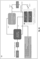
- Figure 1A illustrates building an instruction trace for register renaming according to an embodiment.
- a given LTT-NTB trace could be very long (in terms of number of fuops), so embodiments may include breaking them down into capsules.
- a capsule size may be based on median trace lengths, such as sixteen fuops.
- each trace exceeding a length of sixteen fuops is broken down into capsules of sixteen fuops.
- Each capsule of a trace goes to a different entry in the register renaming cache, all belonging to same set but different ways and have the same tag.
- a register renaming cache hit may mean multiple ways of a set are hitting.
- LTT-NTB trace A (100A) from A1 to An is broken into x+1 capsules or chunks of 16 fuops each (102A, 104A, to 106A) and LTT-NTB trace B (100B) from B1 to Bn is broken into y+1 capsules or chunks of 16 fuops each (102B, 104B, to 106B).
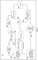
- FIG. 1B illustrates a register renaming pipeline 110 according to an embodiment.
- Register renaming pipeline 110 may be implemented in a processor, processor core, execution core, etc. which may be any type of processor/core, including a general-purpose microprocessor/core, such as a processor/core in the Intel ® Core ® Processor Family or other processor family from Intel ® Corporation or another company, a special purpose processor or microcontroller, or any other device or component in an information processing system in which an embodiment may be implemented.
- a general-purpose microprocessor/core such as a processor/core in the Intel ® Core ® Processor Family or other processor family from Intel ® Corporation or another company, a special purpose processor or microcontroller, or any other device or component in an information processing system in which an embodiment may be implemented.
- register renaming pipeline 110 may be implemented in any of processors 470, 480, or 415 in Figure 4 , processor 500 or one of cores 502A to 502N in Figure 5 , and/or core 690 in Figure 6B , each as described below, in circuitry, logic gates, structures, hardware, etc., all or parts of which may be included in a discrete component and/or integrated into the circuitry of a processing device or any other apparatus in a computer or other information processing system.
- register renaming pipeline 110 includes front end (FE) 112, instruction decode queue (IDQ) 114, legacy rename block 116, lookup block 120, register renaming cache 122, and out-of-order (OOO) block 130.
- FE 112 may correspond to front-end unit 630 in Figure 6B , as described below.
- legacy rename block 116, lookup block 120, and/or register renaming cache 122 may be implemented in rename/allocator unit 652 in Figure 6B , as described below.
- OOO block 130 may correspond to scheduler 656 in Figure 6B , as described below.
- FE 112 may represent circuitry, logic gates, structures, hardware, etc. to fetch, scan, decode, etc. instructions, and generate as an output one or more micro-operations, micro-code entry points, microinstructions, other instructions, or other control signals, which are decoded from, or which otherwise reflect, or are derived from, original instructions.
- the decoding may be implemented using various different mechanisms. Examples of suitable mechanisms include, but are not limited to, look-up tables, hardware implementations, programmable logic arrays (PLAs), microcode read only memories (ROMs), etc.
- FE 112 is coupled to IDQ 114 to provide, for example, fuops at two taken branches per cycle, as well as to lookup block 120.
- Lookup block 120 may represent circuitry, logic gates, structures, hardware, etc., to perform lookups in a register renaming cache 122, e.g., a RAT trap, according to embodiments.
- register renaming cache 122 e.g., a RAT trap
- lookup block 120 is labeled RAT trap lookup and register renaming cache 122 is labeled as RAT trap rename, but only as one specific example of a more general register renaming approach according to embodiments.
- Two capsules (124 and 126), as described above for example, each often to sixteen fuops, are shown within register renaming cache 122.
- Legacy rename block 116 may represent a pipeline implemented in circuitry, logic gates, structures, hardware, etc. to perform register renaming according to an existing approach such as using a RAT. Legacy rename block 116 and register renaming cache 122 are coupled to provide for up to 10 or 16, respectively, fuops to OOO block 130 for execution.
- up to two capsules may have register renamed per cycle based on the information from register renaming cache 122, to match a front end bandwidth of two branches taken per cycle (each of which may correspond to a 16-fuop long capsule, or less if the trace is broken by the end of a taken branch).
- FE 112 may be limited to two taken branches and may be less than sixteen fuops. For that reason, to match the taken branch bandwidth of FE 112, renaming with register renaming cache 122 should also be able to support two taken branches worth of fuops.
- register renaming cache 122 uses two renaming capsules (124 and 126).
- a register renaming cache (e.g., register renaming cache 122) may store the following information for each capsule.
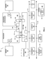
- FIG. 2 illustrates register renaming circuitry 200, including RAT 210 and multiplexers 212, 214, and 216, according to an embodiment.
- Register renaming circuitry 200 may be implemented in a processor, processor core, execution core, etc. which may be any type of processor/core, including a general-purpose microprocessor/core, such as a processor/core in the Intel ® Core ® Processor Family or other processor family from Intel ® Corporation or another company, a special purpose processor or microcontroller, or any other device or component in an information processing system in which an embodiment may be implemented.
- register renaming circuitry 200 may be implemented in any of processors 470, 480, or 415 in Figure 4 , processor 500 or one of cores 502A to 502N in Figure 5 , and/or core 690 in Figure 6B , each as described below, in circuitry, logic gates, structures, hardware, etc., all or parts of which may be included in a discrete component and/or integrated into the circuitry of a processing device or any other apparatus in a computer or other information processing system.
- the source renaming has no complicated control logic to determine the inline dependency and select line of the source renaming multiplexer (e.g., 212) and live-out multiplexer (e.g., 214).
- This select line comes directly from the memory read of the register renaming cache.
- inline destination override logic is not required because the select line for the live-in multiplexer (e.g., 216) comes directly from the register renaming cache read.
- Embodiments may include software assistance to improve hit rates in the register renaming cache (e.g., for large code footprint server workloads). For example, an application developer/compiler may reorganize code to reduce the number of taken branches in the code and better organize the code to reduce the number of live-ins and live-outs for a trace, for improved utilization of register renaming cache ports and storage.
- Embodiments may include profile-guided learning of frequent paths (traces) and re-optimization of source code and the compiler's code generator to minimize register renaming constraints. For example, when the number of register renaming live-ins in sequential code increases, the compiler may optimize the code generated (e.g., similar to how the compiler today reduces register spills and fills).
- information is learned from register renaming operations happening between the last taken target and the next taken branch and stored in the register renaming cache in a capsule for that trace. While replaying register renaming from the register renaming cache, the number of taken branches allowed to be renamed may be limited (e.g., to two). In some cases, if the taken branch density is too high, the bandwidth of register renaming in terms of number of fuops renamed in a cycle will drop. To address this problem, if some branches have a very high probability of being taken, embodiments may utilize software and compiler support to fix the polarity of the branch to static value and not make it look like a branch, thus increasing the bandwidth register renaming according to embodiments.
- the register renaming cache may be under-utilized due to port constraints. Under-utilization may cause bad hit rates in the register renaming cache, resulting in performance loss and power increase.
- only unique logical sources (live-ins) and destinations (live-outs) for a trace are stored in one entry of the register renaming cache.
- the compiler may re-organize code or binary editors may be used to minimize the number of live-ins and live-outs for register renaming traces, thus bolstering hit rates for large footprint workloads common in today's servers.
- FIG. 3 illustrates a method 300 for register renaming according to an embodiment.
- Method 300 may be performed, in full or in part, by and/or in connection with the operation of an apparatus such as that shown Figure 1B and/or Figure 2 ; therefore, all or any portion of the preceding description of or related to Figures 1B and/or Figure 2 may be applicable to method 300.
- Figure 3 as elsewhere in this description and its accompanying figures, references may be made to a RAT trap, but only as one specific example of a more general register renaming approach according to embodiments.
- a register renaming cache lookup is performed, for example, by a lookup block (e.g., lookup block 120 in Figure 1B ) in response to an LTT boundary switch and in parallel with a write to an instruction decode queue (e.g., IDQ 114 in Figure 1B ).
- a lookup block e.g., lookup block 120 in Figure 1B
- an instruction decode queue e.g., IDQ 114 in Figure 1B
- register renaming in response to a register renaming cache miss, register renaming may be performed according to a prior approach (e.g., using a RAT), to provide for register allocation to be performed in 318 and method 300 to continue in 320.
- a prior approach e.g., using a RAT
- register renaming in response to a register renaming cache hit, register renaming may be performed based on information from the register renaming cache, to provide for register allocation to be performed in 318 and method 300 to continue in 330.
- information regarding the properties of the renaming performed in 314 may be learned such that, if it determined in 322 that the register renaming cache is not full, the information may be stored in the register renaming cache in 324. However, if it is determined in 322 that the register renaming cache is full, then, if it is determined in 326 that there is a high taken branch density, then in 328 a compiler or binary editor may re-organize code to reduce taken branches to provide for another relearning for a register renaming cache fill in 324.
- 330 it may be determined whether renaming bandwidth is low due register renaming cache port constraints, and if so, then in 332, a compiler or binary editor may re-organize code to reduce live-ins and live-outs per trace to provide for another relearning for a register renaming cache fill in 324.
- method 300 may return to 310.
- an apparatus e.g., a processor core, processor core, system, system on a chip (SoC), etc.
- the register renaming cache is to store register renaming information associated with an instruction trace.
- the register renaming information is to be learned from a first execution of the instruction trace and is to be used to perform register renaming in connection with a second execution of the instruction trace.
- the front-end circuitry is to provide, based on the instruction trace, operations for execution.
- the lookup circuitry to look in the register renaming cache for entries corresponding to the operations.
- the execution circuitry is to execute the instruction trace.
- the instruction trace is to start at a taken branch target and end at a next taken branch.
- the register renaming information is to include an identifier for each unique logical register read.
- the register renaming information is to include an identifier for each unique logical register written.
- Using the register renaming information to perform register renaming in connection with the second execution of the instruction trace is to be performed in response to a lookup hit in the register renaming cache.
- Learning the register renaming information in connection with the first execution of the instruction trace is to be performed in response to a lookup miss in the register renaming cache.
- the apparatus includes a register alias table to be used to perform register renaming in connection with the first execution of the instruction trace. Using the register alias table to perform register renaming in connection with the first execution of the instruction trace is to be performed in response to a lookup miss in the register renaming cache.
- a method includes learning, from a first execution of an instruction trace, register renaming information; storing, in a register renaming cache, the register renaming information; and using the register renaming information to perform register renaming in connection with a second execution of the instruction trace.
- the instruction trace is to start at a taken branch target and end at a next taken branch.
- the register renaming information is to include an identifier for each unique logical register read.
- the register renaming information is to include an identifier for each unique logical register written.
- the method includes looking in the register renaming cache for an entry corresponding to the instruction trace. Using the register renaming information to perform register renaming in connection with a second execution of the instruction trace is performed in response to looking in the register renaming cache for an entry corresponding to the instruction trace resulting in a hit.
- the method includes using a register alias table to perform register renaming in connection with the first execution of the instruction trace. Using the register alias table to perform register renaming in connection with the first execution of the instruction trace is to be performed in response to looking in the register renaming cache for an entry corresponding to the instruction trace resulting in a miss.
- a method includes profiling code to provide for learning, from a first execution of an instruction trace in the code, register renaming information to be stored in a register renaming cache; and re-organizing the code to reduce register renaming constraints on performing register renaming using the register renaming information from the register renaming cache in connection with a second execution of the instruction trace.
- Re-organizing the code includes re-organizing the code to reduce sequential register live-ins or live-outs.
- Re-organizing the code includes re-organizing the code to reduce taken branches.
- an apparatus may include means for performing any function disclosed herein; an apparatus may include a data storage device that stores code that when executed by a hardware processor or controller causes the hardware processor or controller to perform any method or portion of a method disclosed herein; an apparatus, method, system etc. may be as described in the detailed description; a non-transitory machine-readable medium may store instructions that when executed by a machine causes the machine to perform any method or portion of a method disclosed herein.
- Embodiments may include any details, features, etc. or combinations of details, features, etc. described in this specification.
- FIG. 4 illustrates an example computing system.
- Multiprocessor system 400 is an interfaced system and includes a plurality of processors or cores including a first processor 470 and a second processor 480 coupled via an interface 450 such as a point-to-point (P-P) interconnect, a fabric, and/or bus.
- the first processor 470 and the second processor 480 are homogeneous.
- the first processor 470 and the second processor 480 are heterogenous.
- the example system 400 is shown to have two processors, the system may have three or more processors, or may be a single processor system.
- the computing system is a system on a chip (SoC).
- SoC system on a chip
- Processors 470 and 480 are shown including integrated memory controller (IMC) circuitry 472 and 482, respectively.
- IMC integrated memory controller
- Processor 470 also includes interface circuits 476 and 478; similarly, second processor 480 includes interface circuits 486 and 488.
- Processors 470, 480 may exchange information via the interface 450 using interface circuits 478, 488.
- IMCs 472 and 482 couple the processors 470, 480 to respective memories, namely a memory 432 and a memory 434, which may be portions of main memory locally attached to the respective processors.
- Processors 470, 480 may each exchange information with a network interface (NW I/F) 490 via individual interfaces 452, 454 using interface circuits 476, 494, 486, 498.
- the network interface 490 e.g., one or more of an interconnect, bus, and/or fabric, and in some examples is a chipset
- the coprocessor 438 is a special-purpose processor, such as, for example, a high-throughput processor, a network or communication processor, compression engine, graphics processor, general purpose graphics processing unit (GPGPU), neural-network processing unit (NPU), embedded processor, or the like.
- a shared cache (not shown) may be included in either processor 470, 480 or outside of both processors, yet connected with the processors via an interface such as P-P interconnect, such that either or both processors' local cache information may be stored in the shared cache if a processor is placed into a low power mode.
- Network interface 490 may be coupled to a first interface 416 via interface circuit 496.
- first interface 416 may be an interface such as a Peripheral Component Interconnect (PCI) interconnect, a PCI Express interconnect or another I/O interconnect.
- PCI Peripheral Component Interconnect
- first interface 416 is coupled to a power control unit (PCU) 417, which may include circuitry, software, and/or firmware to perform power management operations with regard to the processors 470, 480 and/or co-processor 438.
- PCU 417 provides control information to a voltage regulator (not shown) to cause the voltage regulator to generate the appropriate regulated voltage.
- PCU 417 also provides control information to control the operating voltage generated.
- PCU 417 may include a variety of power management logic units (circuitry) to perform hardware-based power management.
- Such power management may be wholly processor controlled (e.g., by various processor hardware, and which may be triggered by workload and/or power, thermal or other processor constraints) and/or the power management may be performed responsive to external sources (such as a platform or power management source or system software).
- PCU 417 is illustrated as being present as logic separate from the processor 470 and/or processor 480. In other cases, PCU 417 may execute on a given one or more of cores (not shown) of processor 470 or 480. In some cases, PCU 417 may be implemented as a microcontroller (dedicated or general-purpose) or other control logic configured to execute its own dedicated power management code, sometimes referred to as P-code. In yet other examples, power management operations to be performed by PCU 417 may be implemented externally to a processor, such as by way of a separate power management integrated circuit (PMIC) or another component external to the processor. In yet other examples, power management operations to be performed by PCU 417 may be implemented within BIOS or other system software.
- PMIC power management integrated circuit
- Various I/O devices 414 may be coupled to first interface 416, along with a bus bridge 418 which couples first interface 416 to a second interface 420.
- one or more additional processor(s) 415 such as coprocessors, high throughput many integrated core (MIC) processors, GPGPUs, accelerators (such as graphics accelerators or digital signal processing (DSP) units), field programmable gate arrays (FPGAs), or any other processor, are coupled to first interface 416.
- second interface 420 may be a low pin count (LPC) interface.
- Various devices may be coupled to second interface 420 including, for example, a keyboard and/or mouse 422, communication devices 427 and storage circuitry 428.
- Storage circuitry 428 may be one or more non-transitory machine-readable storage media as described below, such as a disk drive or other mass storage device which may include instructions/code and data 430. Further, an audio I/O 424 may be coupled to second interface 420. Note that other architectures than the point-to-point architecture described above are possible. For example, instead of the point-to-point architecture, a system such as multiprocessor system 400 may implement a multi-drop interface or other such architecture.
- Processor cores may be implemented in different ways, for different purposes, and in different processors.
- implementations of such cores may include: 1) a general purpose in-order core intended for general-purpose computing; 2) a high-performance general purpose out-of-order core intended for general-purpose computing; 3) a special purpose core intended primarily for graphics and/or scientific (throughput) computing.
- Implementations of different processors may include: 1) a CPU including one or more general purpose in-order cores intended for general-purpose computing and/or one or more general purpose out-of-order cores intended for general-purpose computing; and 2) a coprocessor including one or more special purpose cores intended primarily for graphics and/or scientific (throughput) computing.
- Such different processors lead to different computer system architectures, which may include: 1) the coprocessor on a separate chip from the CPU; 2) the coprocessor on a separate die in the same package as a CPU; 3) the coprocessor on the same die as a CPU (in which case, such a coprocessor is sometimes referred to as special purpose logic, such as integrated graphics and/or scientific (throughput) logic, or as special purpose cores); and 4) a system on a chip (SoC) that may be included on the same die as the described CPU (sometimes referred to as the application core(s) or application processor(s)), the above described coprocessor, and additional functionality.
- SoC system on a chip
- FIG. 5 illustrates a block diagram of an example processor and/or SoC 500 that may have one or more cores and an integrated memory controller.
- the solid lined boxes illustrate a processor 500 with a single core 502(A), system agent unit circuitry 510, and a set of one or more interface controller unit(s) circuitry 516, while the optional addition of the dashed lined boxes illustrates an alternative processor 500 with multiple cores 502(A)-(N), a set of one or more integrated memory controller unit(s) circuitry 514 in the system agent unit circuitry 510, and special purpose logic 508, as well as a set of one or more interface controller units circuitry 516.
- the processor 500 may be one of the processors 470 or 480, or co-processor 438 or 415 of FIG. 4 .
- different implementations of the processor 500 may include: 1) a CPU with the special purpose logic 508 being integrated graphics and/or scientific (throughput) logic (which may include one or more cores, not shown), and the cores 502(A)-(N) being one or more general purpose cores (e.g., general purpose in-order cores, general purpose out-of-order cores, or a combination of the two); 2) a coprocessor with the cores 502(A)-(N) being a large number of special purpose cores intended primarily for graphics and/or scientific (throughput); and 3) a coprocessor with the cores 502(A)-(N) being a large number of general purpose in-order cores.
- the special purpose logic 508 being integrated graphics and/or scientific (throughput) logic
- the cores 502(A)-(N) being one or more general purpose cores (e.g., general purpose in-order cores, general purpose out-of-order cores, or a combination of the two)
- the processor 500 may be a general-purpose processor, coprocessor, or special-purpose processor, such as, for example, a network or communication processor, compression engine, graphics processor, GPGPU (general purpose graphics processing unit), a high throughput many integrated cores (MIC) coprocessor (including 30 or more cores), embedded processor, or the like.
- the processor may be implemented on one or more chips.
- the processor 500 may be a part of and/or may be implemented on one or more substrates using any of a number of process technologies, such as, for example, complementary metal oxide semiconductor (CMOS), bipolar CMOS (BiCMOS), P-type metal oxide semiconductor (PMOS), or N-type metal oxide semiconductor (NMOS).
- CMOS complementary metal oxide semiconductor
- BiCMOS bipolar CMOS
- PMOS P-type metal oxide semiconductor
- NMOS N-type metal oxide semiconductor
- a memory hierarchy includes one or more levels of cache unit(s) circuitry 504(A)-(N) within the cores 502(A)-(N), a set of one or more shared cache unit(s) circuitry 506, and external memory (not shown) coupled to the set of integrated memory controller unit(s) circuitry 514.
- the set of one or more shared cache unit(s) circuitry 506 may include one or more mid-level caches, such as level 2 (L2), level 3 (L3), level 4 (L4), or other levels of cache, such as a last level cache (LLC), and/or combinations thereof.
- LLC last level cache
- interface network circuitry 512 e.g., a ring interconnect
- special purpose logic 508 e.g., integrated graphics logic
- set of shared cache unit(s) circuitry 506, and the system agent unit circuitry 510 alternative examples use any number of well-known techniques for interfacing such units.
- coherency is maintained between one or more of the shared cache unit(s) circuitry 506 and cores 502(A)-(N).
- interface controller unit circuitry 516 couples the cores 502 to one or more other devices 518 such as one or more I/O devices, storage, one or more communication devices (e.g., wireless networking, wired networking, etc.), etc.
- the system agent unit circuitry 510 includes those components coordinating and operating cores 502(A)-(N).
- the system agent unit circuitry 510 may include, for example, power control unit (PCU) circuitry and/or display unit circuitry (not shown).
- the PCU may be or may include logic and components needed for regulating the power state of the cores 502(A)-(N) and/or the special purpose logic 508 (e.g., integrated graphics logic).
- the display unit circuitry is for driving one or more externally connected displays.
- the cores 502(A)-(N) may be homogenous in terms of instruction set architecture (ISA). Alternatively, the cores 502(A)-(N) may be heterogeneous in terms of ISA; that is, a subset of the cores 502(A)-(N) may be capable of executing an ISA, while other cores may be capable of executing only a subset of that ISA or another ISA.
- ISA instruction set architecture
- FIG. 6A is a block diagram illustrating both an example in-order pipeline and an example register renaming, out-of-order issue/execution pipeline according to examples.
- FIG. 6B is a block diagram illustrating both an example in-order architecture core and an example register renaming, out-of-order issue/execution architecture core to be included in a processor according to examples.
- the solid lined boxes in FIGS. 6A-B illustrate the in-order pipeline and in-order core, while the optional addition of the dashed lined boxes illustrates the register renaming, out-of-order issue/execution pipeline and core. Given that the in-order aspect is a subset of the out-of-order aspect, the out-of-order aspect will be described.
- Each of the physical register file(s) circuitry 658 represents one or more physical register files, different ones of which store one or more different data types, such as scalar integer, scalar floating-point, packed integer, packed floating-point, vector integer, vector floating-point, status (e.g., an instruction pointer that is the address of the next instruction to be executed), etc.
- the physical register file(s) circuitry 658 includes vector registers unit circuitry, writemask registers unit circuitry, and scalar register unit circuitry. These register units may provide architectural vector registers, vector mask registers, general-purpose registers, etc.
- the execution cluster(s) 660 includes a set of one or more execution unit(s) circuitry 662 and a set of one or more memory access circuitry 664.
- the execution unit(s) circuitry 662 may perform various arithmetic, logic, floating-point or other types of operations (e.g., shifts, addition, subtraction, multiplication) and on various types of data (e.g., scalar integer, scalar floating-point, packed integer, packed floating-point, vector integer, vector floating-point). While some examples may include a number of execution units or execution unit circuitry dedicated to specific functions or sets of functions, other examples may include only one execution unit circuitry or multiple execution units/execution unit circuitry that all perform all functions.
- the scheduler(s) circuitry 656, physical register file(s) circuitry 658, and execution cluster(s) 660 are shown as being possibly plural because certain examples create separate pipelines for certain types of data/operations (e.g., a scalar integer pipeline, a scalar floating-point/packed integer/packed floating-point/vector integer/vector floating-point pipeline, and/or a memory access pipeline that each have their own scheduler circuitry, physical register file(s) circuitry, and/or execution cluster - and in the case of a separate memory access pipeline, certain examples are implemented in which only the execution cluster of this pipeline has the memory access unit(s) circuitry 664). It should also be understood that where separate pipelines are used, one or more of these pipelines may be out-of-order issue/execution and the rest in-order.
- the set of memory access circuitry 664 is coupled to the memory unit circuitry 670, which includes data TLB circuitry 672 coupled to data cache circuitry 674 coupled to level 2 (L2) cache circuitry 676.
- the memory access circuitry 664 may include load unit circuitry, store address unit circuitry, and store data unit circuitry, each of which is coupled to the data TLB circuitry 672 in the memory unit circuitry 670.
- the instruction cache circuitry 634 is further coupled to the level 2 (L2) cache circuitry 676 in the memory unit circuitry 670.
- the instruction cache 634 and the data cache 674 are combined into a single instruction and data cache (not shown) in L2 cache circuitry 676, level 3 (L3) cache circuitry (not shown), and/or main memory.
- the L2 cache circuitry 676 is coupled to one or more other levels of cache and eventually to a main memory.
- Load/store circuits 705 may also generate addresses.
- Branch/jump circuits 707 cause a branch or jump to a memory address depending on the instruction.
- FPU circuits 709 perform floating-point arithmetic.
- the width of the execution unit(s) circuitry 662 varies depending upon the example and can range from 16-bit to 1,024-bit, for example. In some examples, two or more smaller execution units are logically combined to form a larger execution unit (e.g., two 128-bit execution units are logically combined to form a 256-bit execution unit).
- Program code may be applied to input information to perform the functions described herein and generate output information.
- the output information may be applied to one or more output devices, in known fashion.
- a processing system includes any system that has a processor, such as, for example, a digital signal processor (DSP), a microcontroller, an application specific integrated circuit (ASIC), a field programmable gate array (FPGA), a microprocessor, or any combination thereof.
- DSP digital signal processor
- ASIC application specific integrated circuit
- FPGA field programmable gate array
- microprocessor or any combination thereof.
- the program code may be implemented in a high-level procedural or object-oriented programming language to communicate with a processing system.
- the program code may also be implemented in assembly or machine language, if desired.
- the mechanisms described herein are not limited in scope to any particular programming language. In any case, the language may be a compiled or interpreted language.
- Examples of the mechanisms disclosed herein may be implemented in hardware, software, firmware, or a combination of such implementation approaches. Examples may be implemented as computer programs or program code executing on programmable systems comprising at least one processor, a storage system (including volatile and non-volatile memory and/or storage elements), at least one input device, and at least one output device.
- IP Intellectual Property
- IP cores may be stored on a tangible, machine readable medium and supplied to various customers or manufacturing facilities to load into the fabrication machines that make the logic or processor.
- Such machine-readable storage media may include, without limitation, non-transitory, tangible arrangements of articles manufactured or formed by a machine or device, including storage media such as hard disks, any other type of disk including floppy disks, optical disks, compact disk read-only memories (CD-ROMs), compact disk rewritables (CD-RWs), and magneto-optical disks, semiconductor devices such as read-only memories (ROMs), random access memories (RAMs) such as dynamic random access memories (DRAMs), static random access memories (SRAMs), erasable programmable read-only memories (EPROMs), flash memories, electrically erasable programmable read-only memories (EEPROMs), phase change memory (PCM), magnetic or optical cards, or any other type of media suitable for storing electronic instructions.
- storage media such as hard disks, any other type of disk including floppy disks, optical disks, compact disk read-only memories (CD-ROMs), compact disk rewritables (CD-RWs), and magneto-opti
- examples also include non-transitory, tangible machine-readable media containing instructions or containing design data, such as Hardware Description Language (HDL), which defines structures, circuits, apparatuses, processors and/or system features described herein.
- HDL Hardware Description Language
- Such examples may also be referred to as program products.
- Emulation including binary translation, code morphing, etc.
- an instruction converter may be used to convert an instruction from a source instruction set architecture to a target instruction set architecture.
- the instruction converter may translate (e.g., using static binary translation, dynamic binary translation including dynamic compilation), morph, emulate, or otherwise convert an instruction to one or more other instructions to be processed by the core.
- the instruction converter may be implemented in software, hardware, firmware, or a combination thereof.
- the instruction converter may be on processor, off processor, or part on and part off processor.
- FIG. 8 is a block diagram illustrating the use of a software instruction converter to convert binary instructions in a source ISA to binary instructions in a target ISA according to examples.
- the instruction converter is a software instruction converter, although alternatively the instruction converter may be implemented in software, firmware, hardware, or various combinations thereof.
- FIG. 8 shows a program in a high-level language 802 may be compiled using a first ISA compiler 804 to generate first ISA binary code 806 that may be natively executed by a processor with at least one first ISA core 816.
- the processor with at least one first ISA core 816 represents any processor that can perform substantially the same functions as an Intel ® processor with at least one first ISA core by compatibly executing or otherwise processing (1) a substantial portion of the first ISA or (2) object code versions of applications or other software targeted to run on an Intel processor with at least one first ISA core, in order to achieve substantially the same result as a processor with at least one first ISA core.
- the first ISA compiler 804 represents a compiler that is operable to generate first ISA binary code 806 (e.g., object code) that can, with or without additional linkage processing, be executed on the processor with at least one first ISA core 816.
- FIG. 8 shows the program in the high-level language 802 may be compiled using an alternative ISA compiler 808 to generate alternative ISA binary code 810 that may be natively executed by a processor without a first ISA core 814.
- the instruction converter 812 is used to convert the first ISA binary code 806 into code that may be natively executed by the processor without a first ISA core 814.
- This converted code is not necessarily to be the same as the alternative ISA binary code 810; however, the converted code will accomplish the general operation and be made up of instructions from the alternative ISA.
- the instruction converter 812 represents software, firmware, hardware, or a combination thereof that, through emulation, simulation, or any other process, allows a processor or other electronic device that does not have a first ISA processor or core to execute the first ISA binary code 806.
- references to "one example,” “an example,” “one embodiment,” “an embodiment,” etc., indicate that the example or embodiment described may include a particular feature, structure, or characteristic, but every example or embodiment may not necessarily include the particular feature, structure, or characteristic. Moreover, such phrases do not necessarily refer to the same example or embodiment. Further, when a particular feature, structure, or characteristic is described in connection with an example or embodiment, it is submitted that it is within the knowledge of one skilled in the art to affect such feature, structure, or characteristic in connection with other examples or embodiments whether or not explicitly described.
Landscapes
- Engineering & Computer Science (AREA)
- Theoretical Computer Science (AREA)
- Software Systems (AREA)
- Physics & Mathematics (AREA)
- General Engineering & Computer Science (AREA)
- General Physics & Mathematics (AREA)
- Human Computer Interaction (AREA)
- Advance Control (AREA)
Applications Claiming Priority (1)
| Application Number | Priority Date | Filing Date | Title |
|---|---|---|---|
| US18/400,938 US20250217288A1 (en) | 2023-12-29 | 2023-12-29 | Register renaming caching |
Publications (1)
| Publication Number | Publication Date |
|---|---|
| EP4579446A1 true EP4579446A1 (de) | 2025-07-02 |
Family
ID=93432119
Family Applications (1)
| Application Number | Title | Priority Date | Filing Date |
|---|---|---|---|
| EP24211104.5A Pending EP4579446A1 (de) | 2023-12-29 | 2024-11-06 | Cachespeicherung zur änderung der namen von registern |
Country Status (3)
| Country | Link |
|---|---|
| US (1) | US20250217288A1 (de) |
| EP (1) | EP4579446A1 (de) |
| CN (1) | CN120233944A (de) |
Citations (3)
| Publication number | Priority date | Publication date | Assignee | Title |
|---|---|---|---|---|
| US6240509B1 (en) * | 1997-12-16 | 2001-05-29 | Intel Corporation | Out-of-pipeline trace buffer for holding instructions that may be re-executed following misspeculation |
| US20020144098A1 (en) * | 2001-03-28 | 2002-10-03 | Intel Corporation | Register rotation prediction and precomputation |
| US7272701B2 (en) * | 2003-10-22 | 2007-09-18 | Intel Corporation | Method and apparatus for limiting ports in a register alias table having high-bandwidth and low-bandwidth structures |
-
2023
- 2023-12-29 US US18/400,938 patent/US20250217288A1/en active Pending
-
2024
- 2024-11-06 EP EP24211104.5A patent/EP4579446A1/de active Pending
- 2024-12-11 CN CN202411819429.3A patent/CN120233944A/zh active Pending
Patent Citations (3)
| Publication number | Priority date | Publication date | Assignee | Title |
|---|---|---|---|---|
| US6240509B1 (en) * | 1997-12-16 | 2001-05-29 | Intel Corporation | Out-of-pipeline trace buffer for holding instructions that may be re-executed following misspeculation |
| US20020144098A1 (en) * | 2001-03-28 | 2002-10-03 | Intel Corporation | Register rotation prediction and precomputation |
| US7272701B2 (en) * | 2003-10-22 | 2007-09-18 | Intel Corporation | Method and apparatus for limiting ports in a register alias table having high-bandwidth and low-bandwidth structures |
Also Published As
| Publication number | Publication date |
|---|---|
| US20250217288A1 (en) | 2025-07-03 |
| CN120233944A (zh) | 2025-07-01 |
Similar Documents
| Publication | Publication Date | Title |
|---|---|---|
| US11243775B2 (en) | System, apparatus and method for program order queue (POQ) to manage data dependencies in processor having multiple instruction queues | |
| US10678541B2 (en) | Processors having fully-connected interconnects shared by vector conflict instructions and permute instructions | |
| US11907712B2 (en) | Methods, systems, and apparatuses for out-of-order access to a shared microcode sequencer by a clustered decode pipeline | |
| US11354128B2 (en) | Optimized mode transitions through predicting target state | |
| US9367314B2 (en) | Converting conditional short forward branches to computationally equivalent predicated instructions | |
| US12190157B2 (en) | Methods, systems, and apparatuses for scalable port-binding for asymmetric execution ports and allocation widths of a processor | |
| US10579378B2 (en) | Instructions for manipulating a multi-bit predicate register for predicating instruction sequences | |
| US20230401067A1 (en) | Concurrently fetching instructions for multiple decode clusters | |
| US12487762B2 (en) | Flexible provisioning of coherent memory address decoders in hardware | |
| US20240037036A1 (en) | Scheduling merged store operations in compliance with store ordering rules | |
| US10877765B2 (en) | Apparatuses and methods to assign a logical thread to a physical thread | |
| US11126438B2 (en) | System, apparatus and method for a hybrid reservation station for a processor | |
| US12282778B2 (en) | Selective use of branch prediction hints | |
| EP4394594A1 (de) | Flexible virtualisierung von leistungsüberwachung | |
| EP4579446A1 (de) | Cachespeicherung zur änderung der namen von registern | |
| US20260093484A1 (en) | Per allocation cycle micro-operation fusion | |
| US20250110876A1 (en) | Dynamic cache fill priorization | |
| EP4621564A1 (de) | Bandbreitenbewusstes simultanes multi-threading | |
| CN119668697B (zh) | 一种基于预取的处理器加速取指方法及其装置 | |
| EP4202664B1 (de) | System, vorrichtung und verfahren zur drosselung der fusion von mikrooperationen in einem prozessor | |
| WO2024065850A1 (en) | Providing bytecode-level parallelism in a processor using concurrent interval execution | |
| US20250307179A1 (en) | Interconnect flow-control credit loss detection | |
| US20260023564A1 (en) | Unified transfer engine for compute accelerators | |
| US12393427B2 (en) | Core-based speculative page fault list | |
| US20260003622A1 (en) | Processors, methods, and systems fetch and decode at least two in-order sequences of instructions in parallel |
Legal Events
| Date | Code | Title | Description |
|---|---|---|---|
| PUAI | Public reference made under article 153(3) epc to a published international application that has entered the european phase |
Free format text: ORIGINAL CODE: 0009012 |
|
| STAA | Information on the status of an ep patent application or granted ep patent |
Free format text: STATUS: THE APPLICATION HAS BEEN PUBLISHED |
|
| AK | Designated contracting states |
Kind code of ref document: A1 Designated state(s): AL AT BE BG CH CY CZ DE DK EE ES FI FR GB GR HR HU IE IS IT LI LT LU LV MC ME MK MT NL NO PL PT RO RS SE SI SK SM TR |
|
| STAA | Information on the status of an ep patent application or granted ep patent |
Free format text: STATUS: REQUEST FOR EXAMINATION WAS MADE |
|
| STAA | Information on the status of an ep patent application or granted ep patent |
Free format text: STATUS: EXAMINATION IS IN PROGRESS |
|
| 17P | Request for examination filed |
Effective date: 20251222 |
|
| 17Q | First examination report despatched |
Effective date: 20260114 |