EP4579403A1 - Organic light-emitting display panel, display device and display panel encapsulation method - Google Patents
Organic light-emitting display panel, display device and display panel encapsulation method Download PDFInfo
- Publication number
- EP4579403A1 EP4579403A1 EP23864360.5A EP23864360A EP4579403A1 EP 4579403 A1 EP4579403 A1 EP 4579403A1 EP 23864360 A EP23864360 A EP 23864360A EP 4579403 A1 EP4579403 A1 EP 4579403A1
- Authority
- EP
- European Patent Office
- Prior art keywords
- bonding pin
- touch
- touch bonding
- shielding
- display panel
- Prior art date
- Legal status (The legal status is an assumption and is not a legal conclusion. Google has not performed a legal analysis and makes no representation as to the accuracy of the status listed.)
- Pending
Links
Images


Classifications
-
- G—PHYSICS
- G06—COMPUTING OR CALCULATING; COUNTING
- G06F—ELECTRIC DIGITAL DATA PROCESSING
- G06F3/00—Input arrangements for transferring data to be processed into a form capable of being handled by the computer; Output arrangements for transferring data from processing unit to output unit, e.g. interface arrangements
- G06F3/01—Input arrangements or combined input and output arrangements for interaction between user and computer
- G06F3/03—Arrangements for converting the position or the displacement of a member into a coded form
- G06F3/041—Digitisers, e.g. for touch screens or touch pads, characterised by the transducing means
-
- G—PHYSICS
- G06—COMPUTING OR CALCULATING; COUNTING
- G06F—ELECTRIC DIGITAL DATA PROCESSING
- G06F3/00—Input arrangements for transferring data to be processed into a form capable of being handled by the computer; Output arrangements for transferring data from processing unit to output unit, e.g. interface arrangements
- G06F3/01—Input arrangements or combined input and output arrangements for interaction between user and computer
- G06F3/03—Arrangements for converting the position or the displacement of a member into a coded form
- G06F3/041—Digitisers, e.g. for touch screens or touch pads, characterised by the transducing means
- G06F3/0416—Control or interface arrangements specially adapted for digitisers
- G06F3/04164—Connections between sensors and controllers, e.g. routing lines between electrodes and connection pads
-
- G—PHYSICS
- G06—COMPUTING OR CALCULATING; COUNTING
- G06F—ELECTRIC DIGITAL DATA PROCESSING
- G06F3/00—Input arrangements for transferring data to be processed into a form capable of being handled by the computer; Output arrangements for transferring data from processing unit to output unit, e.g. interface arrangements
- G06F3/01—Input arrangements or combined input and output arrangements for interaction between user and computer
- G06F3/03—Arrangements for converting the position or the displacement of a member into a coded form
- G06F3/041—Digitisers, e.g. for touch screens or touch pads, characterised by the transducing means
- G06F3/0412—Digitisers structurally integrated in a display
-
- G—PHYSICS
- G06—COMPUTING OR CALCULATING; COUNTING
- G06F—ELECTRIC DIGITAL DATA PROCESSING
- G06F3/00—Input arrangements for transferring data to be processed into a form capable of being handled by the computer; Output arrangements for transferring data from processing unit to output unit, e.g. interface arrangements
- G06F3/01—Input arrangements or combined input and output arrangements for interaction between user and computer
- G06F3/03—Arrangements for converting the position or the displacement of a member into a coded form
- G06F3/041—Digitisers, e.g. for touch screens or touch pads, characterised by the transducing means
- G06F3/0416—Control or interface arrangements specially adapted for digitisers
-
- H—ELECTRICITY
- H10—SEMICONDUCTOR DEVICES; ELECTRIC SOLID-STATE DEVICES NOT OTHERWISE PROVIDED FOR
- H10K—ORGANIC ELECTRIC SOLID-STATE DEVICES
- H10K50/00—Organic light-emitting devices
- H10K50/80—Constructional details
- H10K50/84—Passivation; Containers; Encapsulations
- H10K50/841—Self-supporting sealing arrangements
-
- H—ELECTRICITY
- H10—SEMICONDUCTOR DEVICES; ELECTRIC SOLID-STATE DEVICES NOT OTHERWISE PROVIDED FOR
- H10K—ORGANIC ELECTRIC SOLID-STATE DEVICES
- H10K50/00—Organic light-emitting devices
- H10K50/80—Constructional details
- H10K50/84—Passivation; Containers; Encapsulations
- H10K50/844—Encapsulations
-
- H—ELECTRICITY
- H10—SEMICONDUCTOR DEVICES; ELECTRIC SOLID-STATE DEVICES NOT OTHERWISE PROVIDED FOR
- H10K—ORGANIC ELECTRIC SOLID-STATE DEVICES
- H10K59/00—Integrated devices, or assemblies of multiple devices, comprising at least one organic light-emitting element covered by group H10K50/00
- H10K59/10—OLED displays
- H10K59/12—Active-matrix OLED [AMOLED] displays
- H10K59/126—Shielding, e.g. light-blocking means over the TFTs
-
- H—ELECTRICITY
- H10—SEMICONDUCTOR DEVICES; ELECTRIC SOLID-STATE DEVICES NOT OTHERWISE PROVIDED FOR
- H10K—ORGANIC ELECTRIC SOLID-STATE DEVICES
- H10K59/00—Integrated devices, or assemblies of multiple devices, comprising at least one organic light-emitting element covered by group H10K50/00
- H10K59/10—OLED displays
- H10K59/12—Active-matrix OLED [AMOLED] displays
- H10K59/131—Interconnections, e.g. wiring lines or terminals
-
- H—ELECTRICITY
- H10—SEMICONDUCTOR DEVICES; ELECTRIC SOLID-STATE DEVICES NOT OTHERWISE PROVIDED FOR
- H10K—ORGANIC ELECTRIC SOLID-STATE DEVICES
- H10K59/00—Integrated devices, or assemblies of multiple devices, comprising at least one organic light-emitting element covered by group H10K50/00
- H10K59/40—OLEDs integrated with touch screens
-
- H—ELECTRICITY
- H10—SEMICONDUCTOR DEVICES; ELECTRIC SOLID-STATE DEVICES NOT OTHERWISE PROVIDED FOR
- H10K—ORGANIC ELECTRIC SOLID-STATE DEVICES
- H10K59/00—Integrated devices, or assemblies of multiple devices, comprising at least one organic light-emitting element covered by group H10K50/00
- H10K59/70—OLEDs integrated with inorganic light-emitting elements, e.g. with inorganic electroluminescent elements
-
- H—ELECTRICITY
- H10—SEMICONDUCTOR DEVICES; ELECTRIC SOLID-STATE DEVICES NOT OTHERWISE PROVIDED FOR
- H10K—ORGANIC ELECTRIC SOLID-STATE DEVICES
- H10K59/00—Integrated devices, or assemblies of multiple devices, comprising at least one organic light-emitting element covered by group H10K50/00
- H10K59/80—Constructional details
- H10K59/87—Passivation; Containers; Encapsulations
- H10K59/871—Self-supporting sealing arrangements
- H10K59/8722—Peripheral sealing arrangements, e.g. adhesives, sealants
-
- H—ELECTRICITY
- H10—SEMICONDUCTOR DEVICES; ELECTRIC SOLID-STATE DEVICES NOT OTHERWISE PROVIDED FOR
- H10K—ORGANIC ELECTRIC SOLID-STATE DEVICES
- H10K71/00—Manufacture or treatment specially adapted for the organic devices covered by this subclass
-
- G—PHYSICS
- G06—COMPUTING OR CALCULATING; COUNTING
- G06F—ELECTRIC DIGITAL DATA PROCESSING
- G06F2203/00—Indexing scheme relating to G06F3/00 - G06F3/048
- G06F2203/041—Indexing scheme relating to G06F3/041 - G06F3/045
- G06F2203/04103—Manufacturing, i.e. details related to manufacturing processes specially suited for touch sensitive devices
-
- G—PHYSICS
- G06—COMPUTING OR CALCULATING; COUNTING
- G06F—ELECTRIC DIGITAL DATA PROCESSING
- G06F2203/00—Indexing scheme relating to G06F3/00 - G06F3/048
- G06F2203/041—Indexing scheme relating to G06F3/041 - G06F3/045
- G06F2203/04107—Shielding in digitiser, i.e. guard or shielding arrangements, mostly for capacitive touchscreens, e.g. driven shields, driven grounds
-
- H—ELECTRICITY
- H10—SEMICONDUCTOR DEVICES; ELECTRIC SOLID-STATE DEVICES NOT OTHERWISE PROVIDED FOR
- H10K—ORGANIC ELECTRIC SOLID-STATE DEVICES
- H10K59/00—Integrated devices, or assemblies of multiple devices, comprising at least one organic light-emitting element covered by group H10K50/00
- H10K59/80—Constructional details
- H10K59/88—Dummy elements, i.e. elements having non-functional features
Definitions
- the present application relates to the field of display technology, and more particularly to an organic light-emitting display panel, a display device, and a method of packaging a display panel.
- An organic electroluminescent display (Organic Light-Emitting Diode) is a display made of organic electroluminescent light-emitting diodes.
- the touch technology of OLED products occupies a large market.
- the technology of making the touch sensing circuit on the OLED cover plate is relatively mature.
- the metal touch lines bonded to the touch region are formed on the cover plate.
- the packaging layer when the packaging layer is packaged, it will cause uneven laser transmittance and hence uneven sintering, which will lead to problems such as overflow width, air bubbles, and cracks in the packaging layer, which will affect the packaging effect and poor cutting.
- the present application discloses an organic light-emitting display panel, including a cover plate, a substrate and a packaging layer.
- the cover plate is arranged opposite to the substrate.
- the packaging layer is disposed between the cover plate and the substrate.
- the organic light-emitting display panel further includes a touch control circuit, and the touch control circuit is formed on the cover plate.
- the edge of the cover plate is provided with at least one touch bonding pin.
- the at least one touch bonding pin is coupled to the touch circuit.
- a plurality of shielding terminals are disposed on both sides of the at least one touch bonding pin.
- the at least one touch bonding pin and the shielding terminals are disposed corresponding to the packaging layer.
- the length of each of the plurality of shielding terminals is consistent with the length of the at least one touch bonding pin, and the widths of the plurality of shielding terminals decrease gradually along a direction away from the at least one touch bonding pin.
- the present application further discloses a display device, which includes an outer cover plate and an organic light-emitting display panel, where the outer cover plate is arranged on the side of a light-emitting surface of the organic light-emitting display panel.
- the present application further discloses a method of packaging a display panel, which is used for packaging an organic light-emitting display panel, the method including the following operations:
- This application arranges a plurality of shielding terminals on both sides of the touch bonding pin, where the length of the plurality of shielding terminals is consistent with the length of the touch bonding pin, and along the direction of getting away from the touch bonding pin, the widths of the plurality of shielding terminals decrease gradually.
- the energy of the laser head can be controlled to be changed or the speed of the laser head can be changed starting in the region where the shielding terminals are disposed, and the shielding terminals whose widths decrease along the direction of getting away from the touch bonding pin can be used to realize an energy buffering effect in the regions where the shielding terminals are present, so as to avoid a large difference caused by a sudden change in laser energy thus leading to the problem that the junction between the region of non-touch bonding pins and the region of touch bonding pins is prone to uneven packaging caused by a large difference of energy mutation.
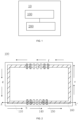
- FIG. 1 is a schematic block diagram of a display device according to the present application.
- FIG. 2 is a schematic diagram of an organic light-emitting display panel according to the present application.
- FIG. 3 is a schematic cross-sectional diagram of FIG. 1 along the section line A-A'.
- FIG. 4 is a schematic diagram of an arrangement of touch bonding pins and shielding terminals in this application.
- the present application discloses a display device 10, including an outer cover plate 200 and an organic light-emitting display panel 100.
- the outer cover plate 200 is disposed on one side of the organic light-emitting display panel 100.
- FIGS. 1 is a schematic block diagram of a display device according to the present application.
- FIG. 2 is a schematic diagram of an organic light-emitting display panel according to the present application.
- FIG. 3 is a schematic cross-sectional diagram of FIG. 1 along the section line A-A'.
- FIG. 4 is a schematic diagram of an arrangement of touch bonding pins and shielding
- the organic light-emitting display panel 100 includes a cover plate 110, a substrate 120 and a packaging layer 130.
- the cover plate 110 is arranged opposite to the substrate 120.
- the packaging layer 130 is disposed between the cover plate 110 and the substrate 120.
- the organic light-emitting display panel 100 further includes a touch circuit 140.
- the touch circuit 140 is formed on the cover plate 110.
- the edge of the cover plate 110 is provided with at least one touch bonding pin 141.
- the at least one touch bonding pin 141 is coupled to the touch circuit 140, and the two sides of the at least one touch bonding pin 141 are respectively provided with a plurality of shielding terminals 150.
- each of the plurality of shielding terminals 150 is consistent with the length of the at least one touch bonding pin 141, and in the direction of getting farther away from the at least one touch bonding pin 141, the widths of the plurality of shielding terminals 150 decrease gradually.
- this application arranges a plurality of shielding terminals 150 on both sides of the at least one touch bonding pin 141, where the length of the plurality of shielding terminals 150 is consistent with the length of the at least one touch bonding pin 141, and along the direction of getting away from the touch bonding pin 141, the widths of the plurality of shielding terminals 150 decrease gradually.
- the energy of the laser head can be slowly increased or the speed of the laser head can be slowly slowed down starting in the region where the shielding terminals 150 are set, and the shielding terminals 150 whose widths decrease along the direction of getting away from the at least one touch bonding pin 141 can be used to realize an energy buffering effect in the regions where the shielding terminals 150 are present, so as to avoid a large difference caused by a sudden change in laser energy thus leading to the problem that the junction between the region of non-touch bonding pins 141 and the region of touch bonding pins 141 is prone to uneven packaging caused by a large difference of energy mutation.
- the packaging layer 130 is glass glue. Because the glass glue itself has certain stability and poor fluidity, it is easier to take shape when coating and packaging, and it can also deform after absorbing heat for attaching and adsorption, hence good packaging effect. Of course, other suitable packaging materials can also be used for packaging, as long as the packaging effect and stability can be guaranteed.
- the direction of the arrow shown in FIG. 2 indicates the direction of a preset path of the laser head.
- the direction of the arrow shown in FIG. 3 is an irradiation direction of the laser light.
- the region where the touch bonding pins 141 are disposed is the touch bonding pin region 180
- the region provided with the shielding terminals 150 is the buffer region 170
- the region without the touch bonding pins 141 and the shielding terminals 150 is the normal region 160.
- the laser light performs sintering and packaging around the edge of the packaging layer 130 along the normal region 160, the buffer region 170 and the touch bonding pin region 180 of the display panel.
- the organic light-emitting display panel has four sides, respectively e, f, g and h.
- the lengths of the touch bonding pins and the shielding terminals are measured extending in a direction parallel to e and g are their lengths, and the widths of the touch bonding pins and the shielding terminals extending along the direction f and h, are their widths.
- the width of the shielding terminal 150 is represented by a.
- the distance from the side of the first shielding terminal 150 away from the second shielding terminal 150 to the side of the second shielding terminal 150 adjacent to the first shielding terminal 150 is represented by b.
- the distance between two adjacent shielding terminals 150 is denoted by c.
- the width of the shielding terminal 150 adjacent to the touch bonding pin 141 is equal to the width of the touch bonding pin 141.
- the spacing between adjacent touch bonding pins 141 is equal.
- the spacing between adjacent shielding terminals 150 is equal.
- the spacing between the touch bonding pin 141 and the shielding terminal 150 that are adjacent to each other is equal.
- the widths of the plurality of shielding terminals 150 decrease gradually according to a first preset value. In this way, the arrangement intervals of the plurality of touch bonding pins and the plurality of shielding terminals are equal and uniform.
- the first preset value is 10um.
- the widths of two adjacent shielding terminals 150 increase gradually along the direction adjacent to the touch bonding pin 141.
- the moving speed of the laser head remains unchanged in this case (that is, the time remains unchanged)
- the power of the laser head increases slowly, the energy of the laser head reaching the touch pin region increases gradually.
- the laser light of the laser head is at its maximum.
- the process of increasing the laser energy of the laser head is a process of gradual and slow increase, and due to the existence of evenly arranged shielding terminals 150, the energy of laser light irradiating each region with a shielding terminal 150 is almost the same during the movement of the laser head. That is, the heat absorbed by the glass glue from laser light is the same. Therefore, in the packaging process, the region of the non-touch bonding pins will not have a large energy difference due to the sudden change of laser light energy, which may otherwise cause uneven packaging. Furthermore, when the laser light reaches the region of the touch bonding pin 141, the energy is also increased as preset to reach the energy value capable of firmly packaging the touch bonding pin region 180. Therefore, the entire packaging process can be made uniform and stable, and the problem of uneven packaging can be avoided.
- the laser light energy of the laser head is gradually reduced.
- the sealing ratio of each region in the entire packaging process is made the same as much as possible, so as to improve the overall packaging effect and achieve a high packaging strength.
- the moving speed of the laser head when the moving speed of the laser head is reduced, the energy accumulation can also be increased due to the longer moving time, and a uniform packaging effect can also be achieved.
- the laser light energy of the laser head is changing, it is also possible to reduce the moving speed of the laser head in combination, where the specific setting and cooperation can be carried out according to the situation, and details are not to be described here.
- the distances between two adjacent shielding terminals 150 can also be decreased by a second preset value at the same time, where the first preset value may be equal to the second preset value. That is, the plurality of the shielding terminals 150 are arranged in such a manner that the widths of the shielding terminals 150 and the distance sbetween two adjacent shielding terminals 150 are arranged in descending order by decrements of the same preset value.
Landscapes
- Engineering & Computer Science (AREA)
- Physics & Mathematics (AREA)
- Theoretical Computer Science (AREA)
- General Engineering & Computer Science (AREA)
- Microelectronics & Electronic Packaging (AREA)
- Optics & Photonics (AREA)
- General Physics & Mathematics (AREA)
- Human Computer Interaction (AREA)
- Inorganic Chemistry (AREA)
- Chemical & Material Sciences (AREA)
- Manufacturing & Machinery (AREA)
- Computer Networks & Wireless Communication (AREA)
- Electroluminescent Light Sources (AREA)
- Devices For Indicating Variable Information By Combining Individual Elements (AREA)
Abstract
Description
- This application claims the priority and benefit of Chinese patent application number
CN202211111292.7, entitled "Organic Light-emitting Display Panel, Display Device, and Method of Packaging Display Panel" and filed September 13, 2022 - The present application relates to the field of display technology, and more particularly to an organic light-emitting display panel, a display device, and a method of packaging a display panel.
- The description provided in this section is intended for the mere purpose of providing background information related to the present application but doesn't necessarily constitute prior art. An organic electroluminescent display (Organic Light-Emitting Diode) is a display made of organic electroluminescent light-emitting diodes.
- Today, the touch technology of OLED products occupies a large market. In particular, the technology of making the touch sensing circuit on the OLED cover plate is relatively mature. In the current technology where the touch capacitive screen is made on the package, the metal touch lines bonded to the touch region are formed on the cover plate. For hard screens, when the packaging layer is packaged, it will cause uneven laser transmittance and hence uneven sintering, which will lead to problems such as overflow width, air bubbles, and cracks in the packaging layer, which will affect the packaging effect and poor cutting.
- At present, by increasing the laser energy or reducing the moving speed of the laser head, laser sintering is performed on the region containing the touch bonding pins to alleviate the problem of uneven sintering. However, if the increased laser energy falls on the reducing the moving speed of the laser head, it cannot be precisely controlled that the energy increase only exists in the touch bonding pin region. Thus, when the laser energy is increased in the normal region, the energy mutation will cause the normal region to form a sudden change in the topography of the packaging layer, which is more likely to cause cracks in the packaging layer, resulting in poor packaging.
- In view of the above, it is therefore one purpose of the present application to provide an organic light-emitting display panel, a display device, and a method of packaging a display panel, which avoid uneven packaging and improve the packaging effect.
- The present application discloses an organic light-emitting display panel, including a cover plate, a substrate and a packaging layer. The cover plate is arranged opposite to the substrate. The packaging layer is disposed between the cover plate and the substrate. The organic light-emitting display panel further includes a touch control circuit, and the touch control circuit is formed on the cover plate. The edge of the cover plate is provided with at least one touch bonding pin. The at least one touch bonding pin is coupled to the touch circuit. A plurality of shielding terminals are disposed on both sides of the at least one touch bonding pin. The at least one touch bonding pin and the shielding terminals are disposed corresponding to the packaging layer. The length of each of the plurality of shielding terminals is consistent with the length of the at least one touch bonding pin, and the widths of the plurality of shielding terminals decrease gradually along a direction away from the at least one touch bonding pin.
- The present application further discloses a display device, which includes an outer cover plate and an organic light-emitting display panel, where the outer cover plate is arranged on the side of a light-emitting surface of the organic light-emitting display panel.
- The present application further discloses a method of packaging a display panel, which is used for packaging an organic light-emitting display panel, the method including the following operations:
- coating a packaging layer at an edge position between the cover plate and the substrate;
- performing laser sintering on the packaging layer of the display panel along a preset path using laser equipment;
- in response to detecting that the laser device has moved to a normal region, sintering the packaging layer in the normal region according to a first preset laser energy and a first preset moving speed;
- in response to detecting that the laser device has moved to a buffer region, gradually increasing the laser energy and/or gradually reducing the moving speed is to sinter the packaging layer in the buffer region; and
- in response to detecting that the laser device has moved to the touch bonding pin region, increasing the laser energy to sinter the packaging layer in a touch bonding pin region;
- wherein touch bonding pins and shielding terminals located on both sides of the touch bonding pins are formed on the cover plate; wherein laser sintering ratios of the normal region, the buffer region and the touch bonding pin region of the laser device are equal.
- This application arranges a plurality of shielding terminals on both sides of the touch bonding pin, where the length of the plurality of shielding terminals is consistent with the length of the touch bonding pin, and along the direction of getting away from the touch bonding pin, the widths of the plurality of shielding terminals decrease gradually. In this way, when performing laser irradiation, the energy of the laser head can be controlled to be changed or the speed of the laser head can be changed starting in the region where the shielding terminals are disposed, and the shielding terminals whose widths decrease along the direction of getting away from the touch bonding pin can be used to realize an energy buffering effect in the regions where the shielding terminals are present, so as to avoid a large difference caused by a sudden change in laser energy thus leading to the problem that the junction between the region of non-touch bonding pins and the region of touch bonding pins is prone to uneven packaging caused by a large difference of energy mutation.
-
-
FIG. 1 is a block diagram of a display device according to the present application. -
FIG. 2 is a schematic diagram of an organic light-emitting display panel according to the present application. -
FIG. 3 is a schematic cross-sectional diagram ofFIG. 2 along the section line A-A'. -
FIG. 4 is a schematic diagram of an arrangement of shielding terminals provided by a first embodiment according to the present application. -
FIG. 5 is a schematic cross-sectional diagram of an organic light-emitting display panel provided in a second embodiment according to the present application. -
FIG. 6 is a flowchart of a method of packaging a display panel according to the present application. -
FIG. 1 is a schematic block diagram of a display device according to the present application.FIG. 2 is a schematic diagram of an organic light-emitting display panel according to the present application.FIG. 3 is a schematic cross-sectional diagram ofFIG. 1 along the section line A-A'.FIG. 4 is a schematic diagram of an arrangement of touch bonding pins and shielding terminals in this application. As shown inFIG. 1 , the present application discloses adisplay device 10, including anouter cover plate 200 and an organic light-emitting display panel 100. Theouter cover plate 200 is disposed on one side of the organic light-emittingdisplay panel 100. In particular, as can be seen fromFIGS. 2-3 , the organic light-emitting display panel 100 includes acover plate 110, asubstrate 120 and apackaging layer 130. Thecover plate 110 is arranged opposite to thesubstrate 120. Thepackaging layer 130 is disposed between thecover plate 110 and thesubstrate 120. The organic light-emitting display panel 100 further includes atouch circuit 140. Thetouch circuit 140 is formed on thecover plate 110. The edge of thecover plate 110 is provided with at least onetouch bonding pin 141. The at least onetouch bonding pin 141 is coupled to thetouch circuit 140, and the two sides of the at least onetouch bonding pin 141 are respectively provided with a plurality ofshielding terminals 150. The length of each of the plurality ofshielding terminals 150 is consistent with the length of the at least onetouch bonding pin 141, and in the direction of getting farther away from the at least onetouch bonding pin 141, the widths of the plurality ofshielding terminals 150 decrease gradually. - Compared with the solution of laser sintering the
region 180 containing the touch bonding pins by increasing the laser energy or reducing the moving speed of the laser head, this application arranges a plurality ofshielding terminals 150 on both sides of the at least onetouch bonding pin 141, where the length of the plurality ofshielding terminals 150 is consistent with the length of the at least onetouch bonding pin 141, and along the direction of getting away from thetouch bonding pin 141, the widths of the plurality ofshielding terminals 150 decrease gradually. In this way, when performing laser irradiation, the energy of the laser head can be slowly increased or the speed of the laser head can be slowly slowed down starting in the region where theshielding terminals 150 are set, and theshielding terminals 150 whose widths decrease along the direction of getting away from the at least onetouch bonding pin 141 can be used to realize an energy buffering effect in the regions where theshielding terminals 150 are present, so as to avoid a large difference caused by a sudden change in laser energy thus leading to the problem that the junction between the region ofnon-touch bonding pins 141 and the region oftouch bonding pins 141 is prone to uneven packaging caused by a large difference of energy mutation. - The
packaging layer 130 is glass glue. Because the glass glue itself has certain stability and poor fluidity, it is easier to take shape when coating and packaging, and it can also deform after absorbing heat for attaching and adsorption, hence good packaging effect. Of course, other suitable packaging materials can also be used for packaging, as long as the packaging effect and stability can be guaranteed. - Hereinafter this application will be described in further detail with reference to the accompanying drawings and some optional embodiments.
- The direction of the arrow shown in
FIG. 2 indicates the direction of a preset path of the laser head. The direction of the arrow shown inFIG. 3 is an irradiation direction of the laser light. As shown inFIGS. 2-3 , the region where the touch bonding pins 141 are disposed is the touchbonding pin region 180, the region provided with the shieldingterminals 150 is thebuffer region 170, and the region without the touch bonding pins 141 and theshielding terminals 150 is thenormal region 160. During packaging, the laser light performs sintering and packaging around the edge of thepackaging layer 130 along thenormal region 160, thebuffer region 170 and the touchbonding pin region 180 of the display panel. - As shown in
FIG. 2 , the organic light-emitting display panel has four sides, respectively e, f, g and h. The lengths of the touch bonding pins and the shielding terminals are measured extending in a direction parallel to e and g are their lengths, and the widths of the touch bonding pins and the shielding terminals extending along the direction f and h, are their widths. - As shown in
FIG. 4 , the width of the shieldingterminal 150 is represented by a. For twoadjacent shielding terminals 150, the distance from the side of thefirst shielding terminal 150 away from thesecond shielding terminal 150 to the side of thesecond shielding terminal 150 adjacent to thefirst shielding terminal 150 is represented by b. The distance between twoadjacent shielding terminals 150 is denoted by c. - As shown in
FIG. 3 , the width of the shieldingterminal 150 adjacent to thetouch bonding pin 141 is equal to the width of thetouch bonding pin 141. The spacing between adjacent touch bonding pins 141 is equal. The spacing betweenadjacent shielding terminals 150 is equal. The spacing between thetouch bonding pin 141 and the shieldingterminal 150 that are adjacent to each other is equal. Along the direction of getting away from thetouch bonding pin 141, the widths of the plurality of shieldingterminals 150 decrease gradually according to a first preset value. In this way, the arrangement intervals of the plurality of touch bonding pins and the plurality of shielding terminals are equal and uniform. The first preset value is 10um. That is, along the direction of getting away from thetouch bonding pin 141, under the condition that the distance c between twoadjacent shielding terminals 150 remains unchanged, a is gradually decreased by the first preset value at the same time. For example: starting from the shielding terminal 150 closest to thetouch bonding pin 141, foradjacent shielding terminals 150, the distance b from the side of thefirst shielding terminal 150 away from thesecond shielding terminal 150 to the side of thesecond shielding terminal 150 adjacent to thefirst shielding terminal 150 is 250um, the width a of thefirst shielding terminal 150 is 130um, the distance c between thefirst shielding terminal 150 and thesecond shielding terminal 150 is 120um, then in this case a is reduced according to the first preset value of 10um. That is, the width a of thesecond shielding terminal 150 is 130um-10um=120um. The width a of thethird shielding terminal 150 is 120um-10um=110um, then b is the sum of the width of thesecond shielding terminal 150 plus the distance between thesecond shielding terminal 150 and thethird shielding terminal 150, namely 120um+120um=240um. That is, the distance b from thesecond shielding terminal 150 to thethird shielding terminal 150 is 250um-10um=240um. By analogy, foradjacent shielding terminals 150, b and a are simultaneously arranged in such a way as to descrease by the first preset value. In this case, along the direction of getting away from thetouch bonding pin 141, the arrangement between every twoadjacent shielding terminals 150 is uniform in proportion. - When the laser light of the laser head performs laser packaging on the region of the
packaging layer 130 along the preset path, when it reaches thebuffer region 170, the widths of twoadjacent shielding terminals 150 increase gradually along the direction adjacent to thetouch bonding pin 141. When controlling the laser head to increase energy slowly, since energy is equal to power multiplied by time, if the moving speed of the laser head remains unchanged in this case (that is, the time remains unchanged), then along the preset path, when the power of the laser head increases slowly, the energy of the laser head reaching the touch pin region increases gradually. When reaching the touchbonding pin region 180, the laser light of the laser head is at its maximum. However, since the process of increasing the laser energy of the laser head is a process of gradual and slow increase, and due to the existence of evenly arranged shieldingterminals 150, the energy of laser light irradiating each region with a shieldingterminal 150 is almost the same during the movement of the laser head. That is, the heat absorbed by the glass glue from laser light is the same. Therefore, in the packaging process, the region of the non-touch bonding pins will not have a large energy difference due to the sudden change of laser light energy, which may otherwise cause uneven packaging. Furthermore, when the laser light reaches the region of thetouch bonding pin 141, the energy is also increased as preset to reach the energy value capable of firmly packaging the touchbonding pin region 180. Therefore, the entire packaging process can be made uniform and stable, and the problem of uneven packaging can be avoided. - On the contrary, when the laser light moves from the touch
bonding pin region 180 to thenormal region 160, the laser light energy of the laser head is gradually reduced. In this case, by slowly reducing the energy in thebuffer region 170, it is possible to avoid changes and cracks etc. in the topography of thepackaging layer 130 caused by sudden changes in energy, and the sealing ratio of each region in the entire packaging process is made the same as much as possible, so as to improve the overall packaging effect and achieve a high packaging strength. - Similarly, when the moving speed of the laser head is reduced, the energy accumulation can also be increased due to the longer moving time, and a uniform packaging effect can also be achieved. In addition, while the laser light energy of the laser head is changing, it is also possible to reduce the moving speed of the laser head in combination, where the specific setting and cooperation can be carried out according to the situation, and details are not to be described here.
- In addition, in this embodiment, along the direction of getting away from the
touch bonding pin 141, while the widths of the plurality of shieldingterminals 150 are decreased by the first preset value, the distances between twoadjacent shielding terminals 150 can also be decreased by a second preset value at the same time, where the first preset value may be equal to the second preset value. That is, the plurality of theshielding terminals 150 are arranged in such a manner that the widths of theshielding terminals 150 and the distance sbetween twoadjacent shielding terminals 150 are arranged in descending order by decrements of the same preset value. In this case, a is reduced by the first preset value of 10um, that is, the width a of thesecond shielding terminal 150 is 130um-10um=120um, and the width a of thethird shielding terminal 150 is 120um-10um=110um. The distance c between thesecond shielding terminal 150 and thethird shielding terminal 150 is reduced by the second preset value of 10um, which is 120um-10um=110um. Then in this case b is the sum of the width of thesecond shielding terminal 150 plus the distance between thesecond shielding terminal 150 and thethird shielding terminal 150, namely 120um+110um=230um. That is, b is 250um-20um=230um. By analogy, by arranging the plurality of shieldingterminals 150 in such a descending manner, since the decreasing value of b is slightly larger, in this case, the shieldingterminals 150 are relatively densely arranged. Thus, one or twomore shielding terminals 150 can be arranged in thebuffer region 170, and the descending arrangement of theshielding terminals 150 is also relatively uniform, which can also achieve a more uniform packaging effect during laser irradiation. - Of course, along the direction of getting away from the
touch bonding pin 141, it is also possible that the widths of the plurality of shieldingterminals 150 decrease gradually by decrements of the first preset value, and the distances between twoadjacent shielding terminals 150 increase by a second preset value, where the first preset value is equal to the second preset value, so that the plurality of shieldingterminals 150 can also be arranged in descending widths. Then, in this case, the spacing between every two shieldingterminals 150 is relatively wide, that is, the plurality of shieldingterminals 150 are arranged sparsely. When the laser is irradiated, the energy of the laser light passing through every two shieldingterminals 150 and irradiating thepackaging layer 130 is more, and so thepackaging layer 130 absorbs th energy and has a relatively better packaging effect with thecover plate 110 and thesubstrate 120. However, since theshielding terminals 150 are still arranged in descending order along the direction of getting away from thetouch bonding pin 141, by the cooperation with the laser head, the energy or moving speed of the laser head can still be controlled to make the packaging uniformity better. - The material of the shielding
terminal 150 is the same as that of thetouch bonding pin 141, and the thickness of the shieldingterminal 150 is equal to the thickness of thetouch bonding pin 141. The same material can be processed by the same manufacturing procedure, thus saving materials and reducing process. The same thickness is adopted, so that when the laser is illuminated, the transmittance of the laser light through the shieldingterminal 150 is consistent with that through thetouch bonding pin 141, thus avoiding the problem of uneven packaging of thepackaging layer 130 caused by uneven transmittance resulting in different light heat absorbed by thepackaging layer 130. - In this embodiment, the shielding
terminal 150 may be a metal material. Since thetouch bonding pin 141 may be made of metal material, the uniformity of light blocking can be achieved. Furthermore, it is relatively easy to control if the energy is increased during laser irradiation, and the energy can be increased in the same proportion. Of course, the shieldingterminal 150 can also be made of a black matrix or a transparent electrode or a color filter material, then the material of the shieldingterminal 150 is different from that of thetouch bonding pin 141. This is beneficial for the device to detect and identify the touchbonding pin region 180, thebuffer region 170 and thenormal region 160, thus better controlling the moving speed or energy of the laser head, make the packaging better. - As shown in
FIG. 3 , the organic light-emittingdisplay panel 100 further includes aninorganic layer 190 disposed between thepackaging layer 130 and thesubstrate 120. It is also possible to coat thepackaging layer 130 after theinorganic layer 190 is first formed on thesubstrate 120. -
FIG. 4 is a schematic diagram of an arrangement of shielding terminals provided by a second embodiment according to the present application. As shown inFIG. 4 , the difference between this embodiment and the first embodiment is that the shielding terminal 150 closest to thetouch bonding pin 141 has aslope 151 on a side adjacent to thetouch bonding pin 141, that is, the shieldingterminal 150 has a triangular structure. When the shieldingterminal 150 is made of a metal material, the metal material itself has the function of blocking light namely it also has the function of reflecting light to a certain extent. By designing the side adjacent to thetouch bonding pin 141 as aslope 151, part of the laser light can be properly reflected, and part of the laser light can be reflected from theslope 151 to thepackaging layer 130 corresponding to the touchbonding pin region 180, so that the heat of laser light absorbed by thepackaging layer 130 at this position can be increased, thereby increasing the packaging adhesive force of thepackaging layer 130 at this position, achieving an ideal uniform packaging effect. - The included angle between the
slope 151 and the side of the cover plate is d. The slope of theslope 151 is greater than or equal to 45° and less than 90°, that is, 45°≤d<90°. When the slope of theslope 151 is larger, the laser light can be reflected to the touchbonding pin region 180 relatively more. Furthermore, in this case, due to the existence of theslope 151, the laser light can be reflected to thetouch bonding pin 141 and then reflected and refracted into the region corresponding to thetouch bonding pin 141. - In order to reflect more laser light energy, a reflective material may also be disposed on the
slope 151, so that more laser light energy can be reflected to thepackaging layer 130 corresponding to the touchbonding pin region 180 in combination with the slope of theslope 151, so that thepackaging layer 130 in this region can absorb more laser light energy, thereby improving the packaging adhesion of thepackaging layer 130 in this region. - When the shielding
terminal 150 is made of a black matrix or a transparent electrode or a color filter material, the light transmittance of theslope 151 can be gradually decreased along the inclined direction of theslope 151. That is, the closer to thecover plate 110, the lower the light transmittance of the shieldingterminal 150 having theslope 151. In this way, the light transmittance is designed differently, and the energy absorption at this position can also be made uniformly when the laser is illuminated, so that the energy mutation at this position is also a process of gradual increase or decrease, so that it is not easy to cause the sudden change in energy at this position to be too large thus resulting in a significant sudden change in the topography of thepackaging layer 130 and affecting the packaging effect. Of course, when the shieldingterminal 150 uses a semi-transparent material, the thickness of the shieldingterminal 150 can be set to be thicker than the thickness of thetouch bonding pin 141, so as to enhance the light-shielding ability of theshielding terminals 150, making the laser light energy absorbed by thebuffer region 170 consistent with that absorbed by the touchbonding pin region 180 and thenormal region 160 as much as possible, so as to avoid the sudden change in the topography of thepackaging layer 130. - In addition, in this embodiment, the shielding terminal 150 closest to the
touch bonding pin 141 can also be other structures with aslope 151. For example: theslope 151 can be arc-shaped, and the arc-shaped arc surface faces thetouch bonding pin 141, which is beneficial to the reflection of laser light. Alternatively, the shieldingterminal 150 can also be a rectangular structure with aslope 151, which can be set according to the actual situation, and at the same time cooperate with the energy or moving speed of the laser light of the laser head to achieve better packaging uniformity. -
FIG. 6 is a flow chart of a method of packaging a display panel according to the present application. As shown inFIG. 6 , the present application further discloses a method of packaging a display panel, which is used for packaging the above-mentioned organic light-emitting display panel, the method including the following operations: - S1: between the cover plate and the substrate, coating the packaging layer at the corresponding edge position;
- S2: laser sintering the packaging layer of the display panel along a preset pathby using laser equipment;
- S3: when it is detected that the laser device moves to the normal region, sintering the packaging layer in the normal region according to a first preset laser energy and a first preset moving speed;
- S4: when it is detected that the laser equipment moves to the buffer region, gradually increasing the laser energy and/or gradually reducing the moving speed to sinter the packaging layer in the buffer region;
- S5: when it is detected that the laser device moves to the touch bonding pin region, increasing the laser energy to sinter the packaging layer in the touch bonding pin region;
- where touch bonding pins and shielding terminals located on both sides of the touch bonding pins are formed on the cover plate; the laser sintering ratio of the laser device in the normal region, the buffer region and the touch bonding pin region is the same, so that the packaging region of the display panel is evenly packaged after packaging.
- In addition, in step 5, the moving speed of the laser head can also be reduced in cooperation with with the light-shielding terminals to make the packaging effect better and the uniformity better. Of course, the laser energy change and the moving speed change of the laser head can also be carried out simultaneously.
- It should be noted that the inventive concept of the present application can be formed into many embodiments, but the length of the application document is limited and so these embodiments cannot be enumerated one by one. The technical features can be arbitrarily combined to form a new embodiment, and the original technical effect may be enhanced after the various embodiments or technical features are combined.
- It should be noted that the limitations of various operations involved in this solution will not be deemed to limit the order of the operations, provided that they do not affect the implementation of the specific solution, so that the operations written earlier may be executed earlier or they may also be executed later or even at the same time. As long as the solution can be implemented, they should all be regarded as falling in the scope of protection of this application.
- The foregoing description is merely a further detailed description of the present application made with reference to some specific illustrative embodiments, and the specific implementations of the present application will not be construed to be limited to these illustrative embodiments. For those having ordinary skill in the technical field to which this application pertains, numerous simple deductions or substitutions may be made without departing from the concept of this application, which shall all be regarded as falling in the scope of protection of this application.
Claims (17)
- An organic light-emitting display panel, comprising:a cover plate;a substrate, arranged opposite to the cover plate;a packaging layer, arranged between the cover plate and the substrate;a touch control circuit formed on the cover plate;at least one touch bonding pin, disposed at an edge of the cover plate and coupled to the touch circuit; anda plurality of shielding terminals, disposed on both sides of the at least one touch bonding pin; wherein the at least one touch bonding pin and the plurality of shielding terminals are disposed corresponding to the packaging layer;wherein a length of each of the plurality of shielding terminal is equal to a length of the at least one touch bonding pin, and wherein widths of the plurality of shielding terminals decrease gradually along a direction of getting farther away from the at least one touch bonding pin.
- The organic light-emitting display panel as recited in claim 1, wherein a width of each shielding terminal adjacent to the at least one touch bonding pin is equal to a width of the at least one touch bonding pin;
wherein a spacing between every two adjacent touch bonding pins is equal, a spacing between every two adjacent shielding terminals is equal, and a spacing between every two touch bonding pin and shielding terminal that are adjacent to each other is equal, and wherein the widths of the plurality of shielding terminals decrease by decrements of a first preset value along the direction of getting farther away from the at least one touch bonding pin. - The organic light-emitting display panel as recited in claim 1, wherein a width of each shielding terminal adjacent to the at least one touch bonding pin is equal to a width of the at least one touch bonding pin; wherein in the direction of getting farther away from the at least one touch bonding pin, the widths of the plurality of shielding terminals decrease by decrements of a first preset value, and distances between every two adjacent shielding terminals decrease by decrements of a second preset value, wherein the first preset value is equal to the second preset value.
- The organic light-emitting display panel as recited in claim 1, wherein a width of each shielding terminal adjacent to the at least one touch bonding pin is equal to a width of the at least one touch bonding pin;
wherein along the direction of getting away from the at least one touch bonding pin, the widths of the plurality of shielding terminals decrease by decrements of a first preset value, and distances between every two adjacent shielding terminals increase by increments of a second preset value, wherein first preset value is equal to the second preset value. - The organic light-emitting display panel as recited in any one of claims 3 to 4, wherein the first preset value and the second preset value are each 10um.
- The organic light-emitting display panel as recited in claim 1, wherein a material of each of the plurality of shielding terminals is the same as that of the at least one touch bonding pin, and wherein a thickness of each of the plurality of shielding terminals is equal to a thickness of the at least one touch bonding pin.
- The organic light-emitting display panel as recited in claim 6, wherein of each shielding terminal adjacent to the at least one touch bonding pin, a side adjacent to the at respective touch bonding pin is a slope, which is greater than or equal to 45° and less than 90°;
wherein the shielding terminal is made of a metal material. - The organic light-emitting display panel as recited in claim 7, wherein the plurality of shielding terminals are each made of a color filter material, and wherein in each shielding terminal adjacent to the at least one touch bonding pin, a light transmittance gradually decreases along an inclination direction of the slope.
- The organic light-emitting display panel as recited in claim 7, wherein a reflective material is disposed on the slope.
- The organic light-emitting display panel as recited in claim 7, wherein a thickness of each of the plurality of shielding terminals is greater than a thickness of the at least one touch bonding pin.
- The organic light-emitting display panel as recited in claim 7, wherein the slope is arc-shaped, and wherein the arc-shaped arc surface faces the touch bonding pin.
- The organic light-emitting display panel as recited in claim 7, wherein the plurality of shielding terminals are each a rectangular structure having a slope.
- The organic light-emitting display panel as recited in claim 1, wherein a material of each of the plurality of shielding terminals is different than that of the at least one touch bonding pin, wherein each of the plurality of shielding terminals is made of a black matrix material.
- The organic light-emitting display panel as recited in claim 1, further comprising an inorganic layer disposed between the packaging layer and the substrate.
- An organic light-emitting display panel, comprising:a cover plate;a substrate, arranged opposite to the cover plate;a packaging layer, arranged between the cover plate and the substrate;a touch control circuit formed on the cover plate;at least one touch bonding pin, disposed at an edge of the cover plate and coupled to the touch circuit;a plurality of shielding terminals, disposed on both sides of the at least one touch bonding pin; wherein the at least one touch bonding pin and the plurality of shielding terminals are disposed corresponding to the packaging layer; wherein a length of each of the plurality of shielding terminal is equal to a length of the at least one touch bonding pin, and wherein widths of the plurality of shielding terminals decrease gradually along a direction of getting farther away from the at least one touch bonding pin;wherein a width of each shielding terminal adjacent to the at least one touch bonding pin is equal to a width of the at least one touch bonding pin; wherein a spacing between every two adjacent touch bonding pins is equal, a spacing between every two adjacent shielding terminals is equal, and a spacing between every two touch bonding pin and shielding terminal that are adjacent to each other is equal, and wherein the widths of the plurality of shielding terminals decrease by decrements of a first preset value along the direction of getting farther away from the at least one touch bonding pin;wherein the first preset value and the second preset value are each 10um;wherein a material of each of the plurality of shielding terminals is identical with that of the at least one touch bonding pin, and wherein a thickness of each of the plurality of shielding terminals is equal to a thickness of the at least one touch bonding pin.
- A display device, comprising an outer cover plate and an organic light-emitting display panel, wherein the outer cover plate is arranged on a side of a light-emitting surface of the organic light-emitting display panel; wherein the organic light-emitting display comprises: a cover plate; a substrate, arranged opposite to the cover plate; a packaging layer, arranged between the cover plate and the substrate; a touch control circuit formed on the cover plate; at least one touch bonding pin, disposed at an edge of the cover plate and coupled to the touch circuit; and a plurality of shielding terminals, disposed on both sides of the at least one touch bonding pin; wherein the at least one touch bonding pin and the plurality of shielding terminals are disposed corresponding to the packaging layer; wherein a length of each of the plurality of shielding terminal is equal to a length of the at least one touch bonding pin, and wherein widths of the plurality of shielding terminals decrease gradually along a direction of getting farther away from the at least one touch bonding pin.
- A method of packaging a display panel, used for packaging an organic light-emitting display panel, the method comprising:coating a packaging layer at an edge position between the cover plate and the substrate;performing laser sintering on the packaging layer of the display panel along a preset path using laser equipment;in response to detecting that the laser device has moved to a normal region, sintering the packaging layer in the normal region according to a first preset laser energy and a first preset moving speed;in response to detecting that the laser device has moved to a buffer region, gradually increasing the laser energy and/or gradually reducing the moving speed to sinter the packaging layer in the buffer region; andin response to detecting that the laser device has moved to a touch bonding pin region, increasing the laser energy to sinter the packaging layer in the touch bonding pin region;wherein the at least one touch bonding pin and the plurality of shielding terminals located on both sides of the at least one touch bonding pin are formed on the cover plate; wherein laser sintering ratios of the normal region, the buffer region and the touch bonding pin region of the laser equipment are equal.
Applications Claiming Priority (2)
| Application Number | Priority Date | Filing Date | Title |
|---|---|---|---|
| CN202211111292.7A CN115202514B (en) | 2022-09-13 | 2022-09-13 | Organic light-emitting display panel, display device, and packaging method for display panel |
| PCT/CN2023/095088 WO2024055621A1 (en) | 2022-09-13 | 2023-05-18 | Organic light-emitting display panel, display device and display panel encapsulation method |
Publications (2)
| Publication Number | Publication Date |
|---|---|
| EP4579403A1 true EP4579403A1 (en) | 2025-07-02 |
| EP4579403A4 EP4579403A4 (en) | 2025-10-29 |
Family
ID=83572869
Family Applications (1)
| Application Number | Title | Priority Date | Filing Date |
|---|---|---|---|
| EP23864360.5A Pending EP4579403A4 (en) | 2022-09-13 | 2023-05-18 | ORGANIC LIGHT-EMPLOYING DISPLAY PANEL, DISPLAY DEVICE AND DISPLAY PANEL ENSEALING METHOD |
Country Status (6)
| Country | Link |
|---|---|
| US (1) | US11895877B1 (en) |
| EP (1) | EP4579403A4 (en) |
| JP (1) | JP7702046B2 (en) |
| KR (1) | KR20250048095A (en) |
| CN (1) | CN115202514B (en) |
| WO (1) | WO2024055621A1 (en) |
Families Citing this family (1)
| Publication number | Priority date | Publication date | Assignee | Title |
|---|---|---|---|---|
| CN115202514B (en) | 2022-09-13 | 2022-12-23 | 惠科股份有限公司 | Organic light-emitting display panel, display device, and packaging method for display panel |
Family Cites Families (23)
| Publication number | Priority date | Publication date | Assignee | Title |
|---|---|---|---|---|
| CN101501808B (en) * | 2005-12-06 | 2011-11-09 | 康宁股份有限公司 | System and method for frit sealing glass packages |
| KR100824531B1 (en) * | 2006-11-10 | 2008-04-22 | 삼성에스디아이 주식회사 | Organic electroluminescent display and manufacturing method |
| KR101135538B1 (en) * | 2009-11-16 | 2012-04-13 | 삼성모바일디스플레이주식회사 | Display device and method for menufacturing display device |
| KR101039982B1 (en) * | 2010-03-18 | 2011-06-09 | 엘지이노텍 주식회사 | Light emitting device and manufacturing method |
| KR101868473B1 (en) * | 2011-08-11 | 2018-06-19 | 엘지디스플레이 주식회사 | Display Device Integrated with Touch Screen |
| TWI569490B (en) * | 2011-11-28 | 2017-02-01 | 半導體能源研究所股份有限公司 | Sealing body, light emitting module, and method of manufacturing the same |
| US9425437B2 (en) * | 2014-11-18 | 2016-08-23 | Samsung Display Co., Ltd. | Method of manufacturing organic light-emitting diode (OLED) display |
| CN104846331B (en) * | 2015-05-28 | 2018-03-23 | 京东方科技集团股份有限公司 | A kind of mask plate and laser package method applied to laser irradiation |
| CN106293210B (en) * | 2016-08-01 | 2018-02-13 | 京东方科技集团股份有限公司 | A kind of touch base plate and preparation method thereof, contact panel, touch control display apparatus |
| KR102557892B1 (en) * | 2016-08-19 | 2023-07-21 | 삼성디스플레이 주식회사 | Display apparatus |
| CN107342371B (en) * | 2017-08-25 | 2019-03-22 | 上海天马有机发光显示技术有限公司 | Organic light-emitting display panel, method for making the same, and organic light-emitting display device |
| JP2019139422A (en) * | 2018-02-08 | 2019-08-22 | 株式会社ジャパンディスプレイ | Detection device and display device with detection function |
| CN108281569B (en) * | 2018-02-08 | 2020-02-14 | 信利(惠州)智能显示有限公司 | Organic light emitting display device and method of fabricating the same |
| CN208608231U (en) * | 2018-05-02 | 2019-03-15 | 云谷(固安)科技有限公司 | Display panels and display devices |
| KR102908145B1 (en) * | 2020-03-06 | 2026-01-06 | 삼성디스플레이 주식회사 | Display device and method of fabricating the same |
| CN114200702A (en) * | 2020-09-17 | 2022-03-18 | 群创光电股份有限公司 | electronic device |
| CN112662727A (en) | 2020-12-16 | 2021-04-16 | 广东省科学院微生物研究所(广东省微生物分析检测中心) | High-throughput analysis and breeding method for functional microorganisms based on extinct dilution culture group |
| CN115623813B (en) * | 2020-12-22 | 2025-09-16 | 厦门天马微电子有限公司 | Display panel, display device and packaging method |
| CN113156727B (en) * | 2021-04-29 | 2022-09-20 | 惠科股份有限公司 | Array substrate, liquid crystal display panel and liquid crystal display device |
| TWI800850B (en) * | 2021-06-18 | 2023-05-01 | 友達光電股份有限公司 | Display device and manufacturing method thereof |
| CN113589571B (en) * | 2021-07-27 | 2024-08-20 | 昆山国显光电有限公司 | Display panel and display device |
| CN216793723U (en) * | 2022-02-07 | 2022-06-21 | 上海和辉光电股份有限公司 | Organic light emitting display device |
| CN115202514B (en) * | 2022-09-13 | 2022-12-23 | 惠科股份有限公司 | Organic light-emitting display panel, display device, and packaging method for display panel |
-
2022
- 2022-09-13 CN CN202211111292.7A patent/CN115202514B/en active Active
-
2023
- 2023-05-18 EP EP23864360.5A patent/EP4579403A4/en active Pending
- 2023-05-18 JP JP2024538108A patent/JP7702046B2/en active Active
- 2023-05-18 KR KR1020257007865A patent/KR20250048095A/en active Pending
- 2023-05-18 WO PCT/CN2023/095088 patent/WO2024055621A1/en not_active Ceased
- 2023-06-26 US US18/214,457 patent/US11895877B1/en active Active
Also Published As
| Publication number | Publication date |
|---|---|
| JP2025502729A (en) | 2025-01-28 |
| EP4579403A4 (en) | 2025-10-29 |
| WO2024055621A1 (en) | 2024-03-21 |
| CN115202514B (en) | 2022-12-23 |
| JP7702046B2 (en) | 2025-07-02 |
| US11895877B1 (en) | 2024-02-06 |
| CN115202514A (en) | 2022-10-18 |
| KR20250048095A (en) | 2025-04-07 |
Similar Documents
| Publication | Publication Date | Title |
|---|---|---|
| US8917362B2 (en) | Touch-sensitive display device | |
| CN104730603B (en) | A kind of anti-reflection layer stack structure and preparation method thereof, substrate and display device | |
| CN109782951B (en) | Touch display panel and display device | |
| CN103943648B (en) | Display device and packaging method thereof | |
| CN115623813B (en) | Display panel, display device and packaging method | |
| US20140007918A1 (en) | Photovoltaic device | |
| US11895877B1 (en) | Organic light-emitting display panel with shielding terminals having varying widths, display device, and method of packaging display panel | |
| CN102354014B (en) | Light guide plate with support ribs and display module using same | |
| CN205028000U (en) | Antireflection liquid crystal disply device | |
| US8641261B2 (en) | Backlight module | |
| TW202032345A (en) | Display panel and display device | |
| CN110703946A (en) | Display panel and display device | |
| WO2022095770A1 (en) | Conductive substrate and electrochromic device | |
| US10564750B2 (en) | Conductive film structure for touch sensor | |
| WO2022227121A1 (en) | Oled display panel | |
| CN105977399B (en) | The method for packing of display panel, display device and display panel | |
| CN209373170U (en) | A side-entry narrow frame backlight module | |
| CN103256563A (en) | Reflective film, backlight module and display device | |
| CN221176255U (en) | Display module, display module and screen based on COB encapsulation | |
| CN223428842U (en) | Display panel and display device | |
| CN220652037U (en) | Display panel and display device | |
| CN224248113U (en) | Integrated touch screen with shielding function | |
| JP3182880U (en) | Touch device | |
| CN216849958U (en) | Back plate glass for photovoltaic module and photovoltaic module with back plate glass | |
| CN217822832U (en) | Back contact photovoltaic module |
Legal Events
| Date | Code | Title | Description |
|---|---|---|---|
| STAA | Information on the status of an ep patent application or granted ep patent |
Free format text: STATUS: THE INTERNATIONAL PUBLICATION HAS BEEN MADE |
|
| PUAI | Public reference made under article 153(3) epc to a published international application that has entered the european phase |
Free format text: ORIGINAL CODE: 0009012 |
|
| STAA | Information on the status of an ep patent application or granted ep patent |
Free format text: STATUS: REQUEST FOR EXAMINATION WAS MADE |
|
| 17P | Request for examination filed |
Effective date: 20250324 |
|
| AK | Designated contracting states |
Kind code of ref document: A1 Designated state(s): AL AT BE BG CH CY CZ DE DK EE ES FI FR GB GR HR HU IE IS IT LI LT LU LV MC ME MK MT NL NO PL PT RO RS SE SI SK SM TR |
|
| A4 | Supplementary search report drawn up and despatched |
Effective date: 20250926 |
|
| RIC1 | Information provided on ipc code assigned before grant |
Ipc: G06F 3/041 20060101AFI20250922BHEP |
|
| DAV | Request for validation of the european patent (deleted) | ||
| DAX | Request for extension of the european patent (deleted) | ||
| STAA | Information on the status of an ep patent application or granted ep patent |
Free format text: STATUS: EXAMINATION IS IN PROGRESS |
|
| 17Q | First examination report despatched |
Effective date: 20260409 |