EP4579326A1 - Display device - Google Patents
Display device Download PDFInfo
- Publication number
- EP4579326A1 EP4579326A1 EP24222704.9A EP24222704A EP4579326A1 EP 4579326 A1 EP4579326 A1 EP 4579326A1 EP 24222704 A EP24222704 A EP 24222704A EP 4579326 A1 EP4579326 A1 EP 4579326A1
- Authority
- EP
- European Patent Office
- Prior art keywords
- transparent substrate
- substrate
- end portion
- display device
- sealing material
- Prior art date
- Legal status (The legal status is an assumption and is not a legal conclusion. Google has not performed a legal analysis and makes no representation as to the accuracy of the status listed.)
- Pending
Links
Images





Classifications
-
- G—PHYSICS
- G02—OPTICS
- G02F—OPTICAL DEVICES OR ARRANGEMENTS FOR THE CONTROL OF LIGHT BY MODIFICATION OF THE OPTICAL PROPERTIES OF THE MEDIA OF THE ELEMENTS INVOLVED THEREIN; NON-LINEAR OPTICS; FREQUENCY-CHANGING OF LIGHT; OPTICAL LOGIC ELEMENTS; OPTICAL ANALOGUE/DIGITAL CONVERTERS
- G02F1/00—Devices or arrangements for the control of the intensity, colour, phase, polarisation or direction of light arriving from an independent light source, e.g. switching, gating or modulating; Non-linear optics
- G02F1/01—Devices or arrangements for the control of the intensity, colour, phase, polarisation or direction of light arriving from an independent light source, e.g. switching, gating or modulating; Non-linear optics for the control of the intensity, phase, polarisation or colour
- G02F1/13—Devices or arrangements for the control of the intensity, colour, phase, polarisation or direction of light arriving from an independent light source, e.g. switching, gating or modulating; Non-linear optics for the control of the intensity, phase, polarisation or colour based on liquid crystals, e.g. single liquid crystal display cells
- G02F1/133—Constructional arrangements; Operation of liquid crystal cells; Circuit arrangements
- G02F1/1333—Constructional arrangements; Manufacturing methods
- G02F1/133368—Cells having two substrates with different characteristics, e.g. different thickness or material
-
- G—PHYSICS
- G02—OPTICS
- G02F—OPTICAL DEVICES OR ARRANGEMENTS FOR THE CONTROL OF LIGHT BY MODIFICATION OF THE OPTICAL PROPERTIES OF THE MEDIA OF THE ELEMENTS INVOLVED THEREIN; NON-LINEAR OPTICS; FREQUENCY-CHANGING OF LIGHT; OPTICAL LOGIC ELEMENTS; OPTICAL ANALOGUE/DIGITAL CONVERTERS
- G02F1/00—Devices or arrangements for the control of the intensity, colour, phase, polarisation or direction of light arriving from an independent light source, e.g. switching, gating or modulating; Non-linear optics
- G02F1/01—Devices or arrangements for the control of the intensity, colour, phase, polarisation or direction of light arriving from an independent light source, e.g. switching, gating or modulating; Non-linear optics for the control of the intensity, phase, polarisation or colour
- G02F1/13—Devices or arrangements for the control of the intensity, colour, phase, polarisation or direction of light arriving from an independent light source, e.g. switching, gating or modulating; Non-linear optics for the control of the intensity, phase, polarisation or colour based on liquid crystals, e.g. single liquid crystal display cells
- G02F1/133—Constructional arrangements; Operation of liquid crystal cells; Circuit arrangements
- G02F1/1333—Constructional arrangements; Manufacturing methods
-
- G—PHYSICS
- G02—OPTICS
- G02B—OPTICAL ELEMENTS, SYSTEMS OR APPARATUS
- G02B30/00—Optical systems or apparatus for producing three-dimensional [3D] effects, e.g. stereoscopic images
- G02B30/20—Optical systems or apparatus for producing three-dimensional [3D] effects, e.g. stereoscopic images by providing first and second parallax images to an observer's left and right eyes
- G02B30/26—Optical systems or apparatus for producing three-dimensional [3D] effects, e.g. stereoscopic images by providing first and second parallax images to an observer's left and right eyes of the autostereoscopic type
- G02B30/30—Optical systems or apparatus for producing three-dimensional [3D] effects, e.g. stereoscopic images by providing first and second parallax images to an observer's left and right eyes of the autostereoscopic type involving parallax barriers
-
- G—PHYSICS
- G02—OPTICS
- G02F—OPTICAL DEVICES OR ARRANGEMENTS FOR THE CONTROL OF LIGHT BY MODIFICATION OF THE OPTICAL PROPERTIES OF THE MEDIA OF THE ELEMENTS INVOLVED THEREIN; NON-LINEAR OPTICS; FREQUENCY-CHANGING OF LIGHT; OPTICAL LOGIC ELEMENTS; OPTICAL ANALOGUE/DIGITAL CONVERTERS
- G02F1/00—Devices or arrangements for the control of the intensity, colour, phase, polarisation or direction of light arriving from an independent light source, e.g. switching, gating or modulating; Non-linear optics
- G02F1/01—Devices or arrangements for the control of the intensity, colour, phase, polarisation or direction of light arriving from an independent light source, e.g. switching, gating or modulating; Non-linear optics for the control of the intensity, phase, polarisation or colour
- G02F1/13—Devices or arrangements for the control of the intensity, colour, phase, polarisation or direction of light arriving from an independent light source, e.g. switching, gating or modulating; Non-linear optics for the control of the intensity, phase, polarisation or colour based on liquid crystals, e.g. single liquid crystal display cells
- G02F1/133—Constructional arrangements; Operation of liquid crystal cells; Circuit arrangements
-
- G—PHYSICS
- G02—OPTICS
- G02F—OPTICAL DEVICES OR ARRANGEMENTS FOR THE CONTROL OF LIGHT BY MODIFICATION OF THE OPTICAL PROPERTIES OF THE MEDIA OF THE ELEMENTS INVOLVED THEREIN; NON-LINEAR OPTICS; FREQUENCY-CHANGING OF LIGHT; OPTICAL LOGIC ELEMENTS; OPTICAL ANALOGUE/DIGITAL CONVERTERS
- G02F1/00—Devices or arrangements for the control of the intensity, colour, phase, polarisation or direction of light arriving from an independent light source, e.g. switching, gating or modulating; Non-linear optics
- G02F1/01—Devices or arrangements for the control of the intensity, colour, phase, polarisation or direction of light arriving from an independent light source, e.g. switching, gating or modulating; Non-linear optics for the control of the intensity, phase, polarisation or colour
- G02F1/13—Devices or arrangements for the control of the intensity, colour, phase, polarisation or direction of light arriving from an independent light source, e.g. switching, gating or modulating; Non-linear optics for the control of the intensity, phase, polarisation or colour based on liquid crystals, e.g. single liquid crystal display cells
- G02F1/133—Constructional arrangements; Operation of liquid crystal cells; Circuit arrangements
- G02F1/1333—Constructional arrangements; Manufacturing methods
- G02F1/13336—Combining plural substrates to produce large-area displays, e.g. tiled displays
-
- G—PHYSICS
- G02—OPTICS
- G02F—OPTICAL DEVICES OR ARRANGEMENTS FOR THE CONTROL OF LIGHT BY MODIFICATION OF THE OPTICAL PROPERTIES OF THE MEDIA OF THE ELEMENTS INVOLVED THEREIN; NON-LINEAR OPTICS; FREQUENCY-CHANGING OF LIGHT; OPTICAL LOGIC ELEMENTS; OPTICAL ANALOGUE/DIGITAL CONVERTERS
- G02F1/00—Devices or arrangements for the control of the intensity, colour, phase, polarisation or direction of light arriving from an independent light source, e.g. switching, gating or modulating; Non-linear optics
- G02F1/01—Devices or arrangements for the control of the intensity, colour, phase, polarisation or direction of light arriving from an independent light source, e.g. switching, gating or modulating; Non-linear optics for the control of the intensity, phase, polarisation or colour
- G02F1/13—Devices or arrangements for the control of the intensity, colour, phase, polarisation or direction of light arriving from an independent light source, e.g. switching, gating or modulating; Non-linear optics for the control of the intensity, phase, polarisation or colour based on liquid crystals, e.g. single liquid crystal display cells
- G02F1/133—Constructional arrangements; Operation of liquid crystal cells; Circuit arrangements
- G02F1/1333—Constructional arrangements; Manufacturing methods
- G02F1/1335—Structural association of cells with optical devices, e.g. polarisers or reflectors
- G02F1/133509—Filters, e.g. light shielding masks
- G02F1/133512—Light shielding layers, e.g. black matrix
-
- G—PHYSICS
- G02—OPTICS
- G02F—OPTICAL DEVICES OR ARRANGEMENTS FOR THE CONTROL OF LIGHT BY MODIFICATION OF THE OPTICAL PROPERTIES OF THE MEDIA OF THE ELEMENTS INVOLVED THEREIN; NON-LINEAR OPTICS; FREQUENCY-CHANGING OF LIGHT; OPTICAL LOGIC ELEMENTS; OPTICAL ANALOGUE/DIGITAL CONVERTERS
- G02F1/00—Devices or arrangements for the control of the intensity, colour, phase, polarisation or direction of light arriving from an independent light source, e.g. switching, gating or modulating; Non-linear optics
- G02F1/01—Devices or arrangements for the control of the intensity, colour, phase, polarisation or direction of light arriving from an independent light source, e.g. switching, gating or modulating; Non-linear optics for the control of the intensity, phase, polarisation or colour
- G02F1/13—Devices or arrangements for the control of the intensity, colour, phase, polarisation or direction of light arriving from an independent light source, e.g. switching, gating or modulating; Non-linear optics for the control of the intensity, phase, polarisation or colour based on liquid crystals, e.g. single liquid crystal display cells
- G02F1/133—Constructional arrangements; Operation of liquid crystal cells; Circuit arrangements
- G02F1/1333—Constructional arrangements; Manufacturing methods
- G02F1/1339—Gaskets; Spacers; Sealing of cells
-
- H—ELECTRICITY
- H04—ELECTRIC COMMUNICATION TECHNIQUE
- H04N—PICTORIAL COMMUNICATION, e.g. TELEVISION
- H04N13/00—Stereoscopic video systems; Multi-view video systems; Details thereof
- H04N13/30—Image reproducers
- H04N13/302—Image reproducers for viewing without the aid of special glasses, i.e. using autostereoscopic displays
- H04N13/31—Image reproducers for viewing without the aid of special glasses, i.e. using autostereoscopic displays using parallax barriers
-
- G—PHYSICS
- G02—OPTICS
- G02F—OPTICAL DEVICES OR ARRANGEMENTS FOR THE CONTROL OF LIGHT BY MODIFICATION OF THE OPTICAL PROPERTIES OF THE MEDIA OF THE ELEMENTS INVOLVED THEREIN; NON-LINEAR OPTICS; FREQUENCY-CHANGING OF LIGHT; OPTICAL LOGIC ELEMENTS; OPTICAL ANALOGUE/DIGITAL CONVERTERS
- G02F1/00—Devices or arrangements for the control of the intensity, colour, phase, polarisation or direction of light arriving from an independent light source, e.g. switching, gating or modulating; Non-linear optics
- G02F1/01—Devices or arrangements for the control of the intensity, colour, phase, polarisation or direction of light arriving from an independent light source, e.g. switching, gating or modulating; Non-linear optics for the control of the intensity, phase, polarisation or colour
- G02F1/13—Devices or arrangements for the control of the intensity, colour, phase, polarisation or direction of light arriving from an independent light source, e.g. switching, gating or modulating; Non-linear optics for the control of the intensity, phase, polarisation or colour based on liquid crystals, e.g. single liquid crystal display cells
- G02F1/133—Constructional arrangements; Operation of liquid crystal cells; Circuit arrangements
- G02F1/1333—Constructional arrangements; Manufacturing methods
- G02F1/133308—Support structures for LCD panels, e.g. frames or bezels
- G02F1/133311—Environmental protection, e.g. against dust or humidity
-
- G—PHYSICS
- G02—OPTICS
- G02F—OPTICAL DEVICES OR ARRANGEMENTS FOR THE CONTROL OF LIGHT BY MODIFICATION OF THE OPTICAL PROPERTIES OF THE MEDIA OF THE ELEMENTS INVOLVED THEREIN; NON-LINEAR OPTICS; FREQUENCY-CHANGING OF LIGHT; OPTICAL LOGIC ELEMENTS; OPTICAL ANALOGUE/DIGITAL CONVERTERS
- G02F2201/00—Constructional arrangements not provided for in groups G02F1/00 - G02F7/00
- G02F2201/50—Protective arrangements
Definitions
- Embodiments described herein relate generally to a display device.
- display devices that display two different images (videos) on a single screen have been put into practical use.
- a display device When such a display device is applied to a car navigation system, for example, it can provide two different images to a plurality of users, such as displaying a map image to the driver of the vehicle and a television image to the passengers.
- a parallax barrier pattern is provided between a transparent substrate made of glass or resin and a thick transparent layer made of an organic layer.
- organic layers generally have low resistance to moisture, if moisture enters the thick transparent layer from an edge of the thick transparent layer, there is a possibility that the parallax barrier pattern may peel off from the transparent substrate due to the moisture that has entered. In this case, display non-uniformity may occur, making it not possible to provide two different images to a plurality of users.
- a first substrate SUB1 array substrate
- a second substrate SUB2 counter-substrate
- the liquid crystal display device 100 achieves two-screen display by displaying two different images (videos) while separating the images (videos) by a parallax barrier pattern 40 described below.
- TFT thin-film transistors
- Each thin film transistor (TFT) 3 for pixel selection is constituted by a gate electrode 6, a gate insulating film 7a, a semiconductor layer 8, a source electrode 9, and a drain electrode 10.
- an interlayer insulating film 11 which is made from an SiN film and the like, is formed so as to cover the source electrode 9, the drain electrode 10, and the insulating film 7.
- a contact hole 11a is formed in the area corresponding to the drain electrode 10.
- a planarization film 12 formed from an organic film made of acrylic resin or the like, is formed. Further, a contact hole 12a is formed in the planarization film 12.
- the pixel electrode 4 is formed on the surface of the flattening film 12, from a transparent electrode of such as indium tin oxide (ITO) or indium zinc oxide (IZO) so as to be connected to the drain electrode 10 via a contact hole 11a and a contact hole 12a.
- ITO indium tin oxide
- IZO indium zinc oxide
- a passivation film 13 which is formed from an SiO 2 , SiN film or the like, is formed on the surface of the planarization film 12 and the pixel electrode 4.
- the common electrode 5 is formed on the surface of the passivation film 13, from a transparent electrode such as of ITO or IZO.
- the common electrode 5 has a plurality of apertures 5a, and is configured so that an electric field is generated between the pixel electrode 4 and the common electrode 5 via the apertures 5a.
- the liquid crystal display device 100 of the FFS mode is configured, in which the liquid crystals are driven by the lateral electric field between the pixel electrode 4 and the common electrode 5.
- an alignment film 14 made from an organic film such as of polyimide is formed on the common electrode 5, and is also formed so as to be in contact with the passivation film 13 via the aperture 5a of the common electrode 5.
- the first transparent substrate 1, the thin-film transistor 3, the interlayer insulating film 11, the planarization film 12, the pixel electrode 4, the passivation film 13, the common electrode 5, and the alignment film 14 constitute the first substrate SUB1.
- a thick transparent layer 20 formed from an organic layer is formed on the surface of a Z2 direction side of the second transparent substrate 2. Further, as shown in FIGS. 2 and 3 , a parallax barrier pattern 40 is formed on the Z2 direction-side surface of the second transparent substrate 2. On the Z2 direction-side surface of the thick transparent layer 20, red (R), green (G), and blue (B) color filters 21 are formed. Note here that the liquid crystal display device 100 includes a plurality of pixels 22 formed therein, and each of the pixels 22 is provided with a respective color filter 21.
- a black matrix 23 made of a resin or the like is formed on the Z2 direction-side surface of the thick transparent layer 20.
- the black matrix 23 is formed on a boundary between each adjacent pair of pixels 22 in plan view, and is formed into a matrix pattern.
- an overcoat layer 24 is formed as a protective film on Z2 direction-side surfaces of the black matrix 23 and the color filter 21.
- an alignment film 25 made from an organic film such as of polyimide is formed on a Z2 direction-side surface of the overcoat layer 24.
- the first substrate SUB1 and the second substrate SUB2 are adhered together by a sealing material 30 (see FIG. 2 ), and a liquid crystal layer 31 is sealed between the alignment film 14 on a first substrate SUB1 side and the alignment film 25 on a second substrate SUB2 side.
- a backlight 50 is provided, and is configured to emit light from the backlight 50 toward the second substrate SUB2 (the Z1 direction side) from the first substrate SUB1.
- the parallax barrier pattern 40 described above is formed, for example, from a resin layer or a metal layer such as of chromium (Cr), aluminum (Al), silver (Ag), or nickel (Ni), and has light-shielding properties. Further as shown in FIG. 1 , the parallax barrier pattern 40 has a plurality of substantially rectangular apertures (slits) 40a formed to extend along a Y direction. The parallax barrier pattern 40 between each adjacent pair of apertures 40a is formed so as to block light. Furthermore, the parallax barrier pattern 40 is configured so that two of the three colors (red (R), green (G), and blue (B)) of the color filters 21 are visible through the apertures 40a of the parallax barrier pattern 40.
- the thick transparent layer 20 is made of an organic layer, it has low resistance to moisture, and if moisture enters the thick transparent layer 20 from an end portion of the thick transparent layer 20, there is a possibility that the parallax barrier pattern 40 may peel off from the second transparent substrate 2 due to the moisture that has entered. If the parallax barrier pattern 40 peels off from the second transparent substrate 2, it is no longer possible to properly direct the light from the backlight 50, thereby problematically making it not possible to achieve two-screen display.
- FIG. 4 is a plan view schematically showing a configuration example of the liquid crystal display device 100 of this embodiment. Note that FIG. 4 illustrates only the first transparent substrate 1, the second transparent substrate 2, and the sealing material 60 among the elements that make up the liquid crystal display device 100.
- the first transparent substrate 1 includes side surfaces 1a and 1b along an X direction and side surfaces 1c and 1d along the Y direction.
- the second transparent substrate 2 includes side surfaces 2a and 2b along the X direction and side surfaces 2c and 2d along the Y direction.
- the extending portion Ex1 provided between the side surfaces 1a and 2a has a width W2, which is greater than a width W1 of the extending portions Ex1 each provided between the side surfaces 1b and 2b, the side surfaces 1c and 2c, and the side surfaces 1d and 2d.
- This configuration is formed because the extending portion Ex1 between the side surfaces 1a and 2a functions as a mounting section, and terminal portions (a pad group) are formed on the extending portion EX1, and the wiring substrates and IC chips that constitute the liquid crystal display device 100 are mounted thereon.
- the interlayer insulating film 11, the planarization film 12, the passivation film 13, and the alignment film 14 are stacked in this order to constitute the first substrate SUB1.
- the elements that make up the thin film transistor 3 for selecting pixels shown in FIG. 3 , the pixel electrodes 4, and the common electrode 5 are omitted from the illustration, but these elements are disposed between the first transparent substrate 1 and the alignment film 14 as shown in FIG. 3 .
- the first transparent substrate 1 includes the extending portion Ex1 between the side surface 1b and the side surface 2b of the second transparent substrate 2.
- the sealing material 60 is provided so as to cover the end portion (the side surface 2b) of the second transparent substrate 2, the end portion of the thick transparent layer 20, the end portion of the color filter 21, and the end portion of the overcoat layer 23 (that is, the end portion of the second substrate SUB2).
- the sealing material 60 is formed, for example, from acrylic resin, epoxy resin, or a combination of these. Note here that the sealing material 60 should preferably be formed of a material having a moisture resistance higher than that of the thick transparent layer 20.
- the sealing material 60 is provided, for example, in a processing step after the adhesion of the first substrate SUB1 and the second substrate SUB2 together by the sealing material 30, and in a processing step of forming a protective film (not shown) for protecting the IC chips and the like (not shown), so as to cover the end portion of the second substrate SUB2, which includes the end portion of the thick transparent layer 20.
- FIG. 5 the cross-section of the liquid crystal display device 100 taken along the line C1-D1 in FIG. 4 is shown, but the cross-sections of the liquid crystal display device 100 along the line C2-D2 and line C3-D3 line in FIG. 4 have a similar structure.
- an end potion of the thick film transparent layer 20 are covered by the sealing material 60 provided on the extending portion Ex1.
- the sealing material 60 is provided so to cover an end portion of the thick transparent layer 20 other than the end portion on the mounting portion side described above, but the configuration is not limited to this.
- the sealing material 60 may as well be provided in a rectangular frame shape, as shown in FIG. 6 , so as to cover the entire circumference of the end portions of the second transparent substrate 2, including the entire circumference of the end portions of the thick film transparent layer 20 (that is, the side surfaces 2a to 2d) .
- the first modified example is different from the configuration shown in FIGS. 4 and 5 in that a cover member 28, which will be described later, is additionally provided on the second transparent substrate 2.
- a cover member 28 which will be described later
- FIG. 7 is a plan view schematically showing a configuration example of the liquid crystal display device 100 according to the first modified example. Note that in FIG. 7 , among the elements that make up the liquid crystal display device 100, only the first transparent substrate 1, the second transparent substrate 2, the sealing material 60, and the cover member 28 are illustrated.
- the cover member 28 includes side surfaces 28a and 28b along the X direction and side surfaces 28c and 28d along the Y direction.
- the side surface 28a of the cover member 28 overlaps the side surface 1a of the first transparent substrate 1.
- the side surfaces 28b, 28c, and 28d of the cover member 28 overlap the side surfaces 1b, 1c, and 1d of the first transparent substrate 1, respectively.
- the side surface 28a of the cover member 28 does not overlap the side surface 2a of the second transparent substrate 2.
- the side surfaces 28b, 28c, and 28d of the cover member 28 do not overlap the side surfaces 2b, 2c, and 2d of the second transparent substrate 2, respectively.
- the cover member 28 includes extending portions Ex2 (second extending portions) each between the side surfaces 28a and 2a, between the side surfaces 28b and 2b, between the side surfaces 28c and 2c, and between the side surfaces 28d and 2d.
- the sealing material 60 is provided so as to cover the end portion of the second transparent substrate 2, which is other than the end portions on the mounting side edge (the end portion of the thick transparent layer 20, a more detail of which will be described later).
- FIG. 7 illustrates the case where the side surfaces 28a to 28d of the cover member 28 and the side surfaces 1a to 1d of the first transparent substrate 1 overlap respectively each other in plan view, but the configuration is not limited to this.
- the side surfaces 28a to 28d of the cover member 28 and the side surfaces 1a to 1d of the first transparent substrate 1 do not necessarily have to overlap in plan view.
- FIG. 8 is a cross-sectional view schematically showing the liquid crystal display device 100 taken along the line E-F in FIG. 7 .
- a polarizer 26 is disposed on a Z1 direction-side surface of the second transparent substrate 2. Further, the cover member 28 is disposed on the Z1 direction side of the polarizer 26 via an adhesive layer 27.
- the cover member 28 can be made of a glass substrate or a resin substrate, for example.
- the cover member 28 includes side surfaces 28a and 28b along the X direction and side surfaces 28c and 28d along the Y direction.
- the side surfaces 28b, 28c, and 28d of the cover member 28 do not overlap the side surfaces 1b, 1c, and 1d of the first transparent substrate 1 and the side surfaces 2b, 2c, and 2d of the second transparent substrate 2, respectively.
- the side surface 28a of the cover member 28 overlaps the side surface 1a of the first transparent substrate 1, but does not overlap the side surface 2a of the second transparent substrate 2.
- the cover member 28 includes extending portions Ex2 each located between the side surfaces 28a and 2a, between the side surfaces 28b and 2b, between the side surfaces 28c and 2c, and between the side surfaces 28d and 2d.
- the sealing material 60 is provided so as to cover the end portions of the first transparent substrate 1 and the second transparent substrate 2, other than the end portion on the mounting portion side (the end portions of the thick transparent layer 20, a detail of which will be described later).
- FIG. 9 shows the case where the side surface 28a of the cover member 28 and the side surface 1a of the first transparent substrate 1 overlap each other in plan view, but the configuration is not limited to this.
- the side surface 28a of the cover member 28 and the side surface 1a of the first transparent substrate 1 do not necessarily have to overlap each other in plan view.
- FIG. 10 is a cross-sectional view schematically showing the liquid crystal display device 100 taken along the line G-H in FIG. 9 .
- a polarizer 26 is disposed on a Z1 direction-side surface of the second transparent substrate 2. Further, the cover member 28 is disposed on the Z1 direction side of the polarizer 26 via an adhesive layer 27.
- the cover member 28 can be made of a glass substrate or a resin substrate, for example.
- the sealing material 60 is provided to cover the end portion of the first substrate SUB1 and the end portion of the second substrate SUB2, which includes the thick film transparent layer 20.
- the configuration of the end portion of the thick film transparent layer 20 still remains unchanged, and is covered by the sealing material 60 provided under the extending portion Ex2. Therefore, as in the case of the configuration shown in FIGS. 4 and 5 , it is possible to suppress moisture from entering the thick transparent layer 20 from the end portion of the thick transparent layer 20, and to prevent the parallax barrier pattern 40 from peeling off from the second transparent substrate 2.
- the third modified example is different from the configuration shown in FIGS. 4 and 5 in that the first transparent substrate 1 does not have an extending portion Ex1 other than the mounting portion.
- the parts that are different from those of the configuration shown in FIGS. 4 and 5 will be explained, and the parts that are similar to those of the configuration shown in FIGS. 4 and 5 will be omitted.
- the sealing material 60 is provided on the end portions other than the end portion of the mounting portion side.
Landscapes
- Physics & Mathematics (AREA)
- Nonlinear Science (AREA)
- Optics & Photonics (AREA)
- General Physics & Mathematics (AREA)
- Crystallography & Structural Chemistry (AREA)
- Chemical & Material Sciences (AREA)
- Mathematical Physics (AREA)
- Devices For Indicating Variable Information By Combining Individual Elements (AREA)
- Engineering & Computer Science (AREA)
- Multimedia (AREA)
- Signal Processing (AREA)
- Liquid Crystal (AREA)
- Electroluminescent Light Sources (AREA)
Abstract
According to one embodiment, a display device (100) includes a first substrate (SUB1) including a first transparent substrate (1), a second substrate (SUB2) including a second transparent substrate (2), a parallax barrier pattern (40) formed on a surface on a first substrate (SUB1) side of the second transparent substrate (2), and an organic layer (20) which covers the second transparent substrate (2) and the parallax barrier pattern (40), a liquid crystal layer (31), and a sealing material (60) which covers an end portion of the organic layer (20), and the first transparent substrate (1) extends beyond the second transparent substrate (2) and includes a mounting portion (Ex1) on which a circuit board is mounted, and the sealing material (60) covers an end portion of the organic layer (20), other than an end portion on a mounting portion (Ex1) side of the end portion.
Description
- Embodiments described herein relate generally to a display device.
- In recent years, display devices that display two different images (videos) on a single screen have been put into practical use. When such a display device is applied to a car navigation system, for example, it can provide two different images to a plurality of users, such as displaying a map image to the driver of the vehicle and a television image to the passengers.
- In such a display device, in order to display two different images on a single screen, a parallax barrier pattern is provided between a transparent substrate made of glass or resin and a thick transparent layer made of an organic layer. Here, since organic layers generally have low resistance to moisture, if moisture enters the thick transparent layer from an edge of the thick transparent layer, there is a possibility that the parallax barrier pattern may peel off from the transparent substrate due to the moisture that has entered. In this case, display non-uniformity may occur, making it not possible to provide two different images to a plurality of users.
-
-
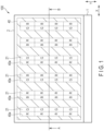
FIG. 1 is a plan view schematically showing a configuration example of a liquid crystal display device which can realize two-screen display. -
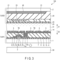
FIG. 2 is a cross-sectional view schematically showing the liquid crystal display panel taken along the line A-B inFIG. 1 . -
FIG. 3 is a plan view schematically showing a configuration example of the liquid crystal display device which can realize two-screen display. -
FIG. 4 is a plan view schematically showing a configuration example of a liquid crystal display device according to an embodiment. -
FIG. 5 is a cross-sectional view schematically showing the liquid crystal display panel taken along the line C1-D1 inFIG. 4 . -
FIG. 6 is a plan view schematically showing another configuration example of the liquid crystal display device according to the embodiment. -
FIG. 7 is a plan view schematically showing a configuration example of a liquid crystal display device according to the first modified example. -
FIG. 8 is a cross-sectional view schematically showing the liquid crystal display panel taken along the line E-F inFIG. 7 . -
FIG. 9 is a plan view schematically showing a configuration example of a liquid crystal display device according to the second modified example. -
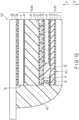
FIG. 10 is a cross-sectional view schematically showing the liquid crystal display panel taken along the line G-H inFIG. 9 . -
FIG. 11 is a plan view schematically showing a configuration example of a liquid crystal display device according to the third modified example. -
FIG. 12 is a cross-sectional view schematically showing the liquid crystal display panel taken along the line I-J inFIG. 11 . - In general, according to one embodiment, a display device includes a first substrate including a first transparent substrate, a second substrate opposing the first substrate and including a second transparent substrate, a parallax barrier pattern formed on a surface on a first substrate side of the second transparent substrate, and an organic layer which covers the second transparent substrate and the parallax barrier pattern, a liquid crystal layer sealed between the first substrate and the second substrate, and a sealing material which covers an end portion of the organic layer. The first transparent substrate extends beyond the second transparent substrate and includes a mounting portion on which a circuit board is mounted. The sealing material covers an end portion of the organic layer, other than an end portion on a mounting portion side of the end portion.
- Embodiments will be described hereinafter with reference to the accompanying drawings.
- Note that the disclosure is merely an example, and proper changes within the spirit of the invention, which are easily conceivable by a skilled person, are included in the scope of the invention as a matter of course. In addition, in some cases, in order to make the description clearer, the widths, thicknesses, shapes, etc., of the respective parts are schematically illustrated in the drawings, compared to the actual modes. However, the schematic illustration is merely an example, and adds no restrictions to the interpretation of the invention. Besides, in the specification and drawings, the same or similar elements as or to those described in connection with preceding drawings or those exhibiting similar functions are denoted by like reference numerals, and a detailed description thereof is omitted unless otherwise necessary.
- First, with reference to
FIGS. 1 to 3 , a configuration example of a liquidcrystal display device 100 that can achieve two-screen display in which two different images (videos) are that displayed on a single screen will be described. This embodiment will be described in connection with the case where the liquidcrystal display device 100 is a liquid crystal display device of a system referred to as the fringe field switching (FFS) mode. Further, the liquidcrystal display device 100 is also an example of a "display device" that can achieve two-screen display. - In the liquid
crystal display device 100, as shown inFIGS. 1 to 3 , a first substrate SUB1 (array substrate) including a firsttransparent substrate 1 and a second substrate SUB2 (counter-substrate) including a secondtransparent substrate 2 are disposed to oppose each other. The liquidcrystal display device 100 achieves two-screen display by displaying two different images (videos) while separating the images (videos) by aparallax barrier pattern 40 described below. - On a surface of a Z1 direction side of the first
transparent substrate 1, thin-film transistors (TFT) 3 for selecting pixels,pixel electrodes 4, and acommon electrode 5 are formed. - Further, as a detailed cross-sectional structure of a single pixel, a
gate electrode 6 is provided on the Z1-direction side surface of the firsttransparent substrate 1 as shown inFIG. 3 . Further, on thegate electrode 6 and the first substrate SUB1, aninsulating film 7 including agate insulating film 7a formed from an SiN film, an SiO2 film or the like, is formed. Furthermore, asemiconductor layer 8 having a two-layer structure (not shown) constituted by an a-Si layer as a lower layer and an n+a-Si layer having has n-type conductivity as an upper layer, is formed so as to overlap thegate electrode 6 via thegate insulating film 7a in plan view. - On the
semiconductor layer 8, asource electrode 9 and adrain electrode 10 are formed so as to overlap thegate electrode 6 in plan view. The area of thesemiconductor layer 8, which is sandwiched between thesource electrode 9 and thedrain electrode 10 in plan view, functions as achannel region 8a. Each thin film transistor (TFT) 3 for pixel selection is constituted by agate electrode 6, a gateinsulating film 7a, asemiconductor layer 8, asource electrode 9, and adrain electrode 10. - Further, an
interlayer insulating film 11, which is made from an SiN film and the like, is formed so as to cover thesource electrode 9, thedrain electrode 10, and theinsulating film 7. In theinterlayer insulating film 11, a contact hole 11a is formed in the area corresponding to thedrain electrode 10. On the surface of theinterlayer insulating film 11, aplanarization film 12 formed from an organic film made of acrylic resin or the like, is formed. Further, a contact hole 12a is formed in theplanarization film 12. Furthermore, thepixel electrode 4 is formed on the surface of theflattening film 12, from a transparent electrode of such as indium tin oxide (ITO) or indium zinc oxide (IZO) so as to be connected to thedrain electrode 10 via a contact hole 11a and a contact hole 12a. - Further, on the surface of the
planarization film 12 and thepixel electrode 4, apassivation film 13, which is formed from an SiO2, SiN film or the like, is formed. Furthermore, thecommon electrode 5 is formed on the surface of thepassivation film 13, from a transparent electrode such as of ITO or IZO. Thecommon electrode 5 has a plurality ofapertures 5a, and is configured so that an electric field is generated between thepixel electrode 4 and thecommon electrode 5 via theapertures 5a. As described above, the liquidcrystal display device 100 of the FFS mode is configured, in which the liquid crystals are driven by the lateral electric field between thepixel electrode 4 and thecommon electrode 5. - Moreover, on the
common electrode 5, analignment film 14 made from an organic film such as of polyimide is formed. Thealignment film 14 is formed so as to cover the surface of thecommon electrode 5, and is also formed so as to be in contact with thepassivation film 13 via theaperture 5a of thecommon electrode 5. With this configuration, the firsttransparent substrate 1, the thin-film transistor 3, theinterlayer insulating film 11, theplanarization film 12, thepixel electrode 4, thepassivation film 13, thecommon electrode 5, and thealignment film 14 constitute the first substrate SUB1. - As shown in
FIGS. 2 and3 , on the surface of a Z2 direction side of the secondtransparent substrate 2, a thicktransparent layer 20 formed from an organic layer, is formed. Further, as shown inFIGS. 2 and3 , aparallax barrier pattern 40 is formed on the Z2 direction-side surface of the secondtransparent substrate 2. On the Z2 direction-side surface of the thicktransparent layer 20, red (R), green (G), and blue (B)color filters 21 are formed. Note here that the liquidcrystal display device 100 includes a plurality ofpixels 22 formed therein, and each of thepixels 22 is provided with arespective color filter 21. - Further, as shown in
FIG. 3 , ablack matrix 23 made of a resin or the like is formed on the Z2 direction-side surface of the thicktransparent layer 20. Theblack matrix 23 is formed on a boundary between each adjacent pair ofpixels 22 in plan view, and is formed into a matrix pattern. Further, anovercoat layer 24 is formed as a protective film on Z2 direction-side surfaces of theblack matrix 23 and thecolor filter 21. Furthermore, analignment film 25 made from an organic film such as of polyimide is formed on a Z2 direction-side surface of theovercoat layer 24. Thus, the secondtransparent substrate 2, the thicktransparent layer 20, theparallax barrier pattern 40, thecolor filter 21, theblack matrix 23, theovercoat layer 24, and thealignment film 25 constitute the second substrate SUB2. - The first substrate SUB1 and the second substrate SUB2 are adhered together by a sealing material 30 (see
FIG. 2 ), and aliquid crystal layer 31 is sealed between thealignment film 14 on a first substrate SUB1 side and thealignment film 25 on a second substrate SUB2 side. On the Z2 direction side of the first substrate SUB1, abacklight 50 is provided, and is configured to emit light from thebacklight 50 toward the second substrate SUB2 (the Z1 direction side) from the first substrate SUB1. - The
parallax barrier pattern 40 described above is formed, for example, from a resin layer or a metal layer such as of chromium (Cr), aluminum (Al), silver (Ag), or nickel (Ni), and has light-shielding properties. Further as shown inFIG. 1 , theparallax barrier pattern 40 has a plurality of substantially rectangular apertures (slits) 40a formed to extend along a Y direction. Theparallax barrier pattern 40 between each adjacent pair ofapertures 40a is formed so as to block light. Furthermore, theparallax barrier pattern 40 is configured so that two of the three colors (red (R), green (G), and blue (B)) of thecolor filters 21 are visible through theapertures 40a of theparallax barrier pattern 40. - Here, incidentally, since the thick
transparent layer 20 is made of an organic layer, it has low resistance to moisture, and if moisture enters the thicktransparent layer 20 from an end portion of the thicktransparent layer 20, there is a possibility that theparallax barrier pattern 40 may peel off from the secondtransparent substrate 2 due to the moisture that has entered. If theparallax barrier pattern 40 peels off from the secondtransparent substrate 2, it is no longer possible to properly direct the light from thebacklight 50, thereby problematically making it not possible to achieve two-screen display. - To avoid this, in the liquid
crystal display device 100 of this embodiment, the end portion of the thicktransparent layer 20 is covered by a sealing material 60m which will be described later, thereby preventing moisture from entering the thicktransparent layer 20. A configuration example of the liquidcrystal display device 100 according to this embodiment will now be described with reference toFIGS. 4 and5 . -
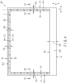
FIG. 4 is a plan view schematically showing a configuration example of the liquidcrystal display device 100 of this embodiment. Note thatFIG. 4 illustrates only the firsttransparent substrate 1, the secondtransparent substrate 2, and the sealingmaterial 60 among the elements that make up the liquidcrystal display device 100. - The first
transparent substrate 1 includes side surfaces 1a and 1b along an X direction andside surfaces transparent substrate 2 includes side surfaces 2a and 2b along the X direction andside surfaces - In plan view, the
side surface 1a of the firsttransparent substrate 1 and theside surface 2a of the secondtransparent substrate 2 do not overlap each other. Similarly, in plan view, the side surfaces 1b and 2b, the side surfaces 1c and 2c, and the side surfaces 1d and 2d do not overlap each other, respectively. The firsttransparent substrate 1 includes extending portions Ex1 (first extending portions) each between the side surfaces 1a and 2a, between the side surfaces 1b and 2b, between the sides surface 1c and 2c, and between the side surfaces 1d and 2d. In the example shown inFIG. 4 , the extending portion Ex1 provided between the side surfaces 1a and 2a has a width W2, which is greater than a width W1 of the extending portions Ex1 each provided between the side surfaces 1b and 2b, the side surfaces 1c and 2c, and the side surfaces 1d and 2d. This configuration is formed because the extending portion Ex1 between the side surfaces 1a and 2a functions as a mounting section, and terminal portions (a pad group) are formed on the extending portion EX1, and the wiring substrates and IC chips that constitute the liquidcrystal display device 100 are mounted thereon. - On the extending portions Ex1 of the first
transparent substrate 1, the sealingmaterial 60 is provided so as to cover the end portions of the secondtransparent substrate 2 except for the end portions of the mounting side described above (that is, the side surfaces 2b to 2d other than theside surface 2a) (the end portion of the thicktransparent layer 20, a more detail thereof will be described later). In other words, the sealingmaterial 60 is provided to cover the end portion (the end portion of the thick film transparent layer 20) of the secondtransparent substrate 2 on the extending portions EX1 other than the extending portion EX1 that functions as the mounting portion. The width W3 of the sealingmaterial 60 should preferably be set to 0.5 mm to 1.5 mm, for example. -
FIG. 5 is a cross-sectional view schematically showing the liquidcrystal display device 100 taken along the line C1-D1 inFIG. 4 . - As shown in
FIG. 5 , on a Z1 direction side of the firsttransparent substrate 1, theinterlayer insulating film 11, theplanarization film 12, thepassivation film 13, and thealignment film 14 are stacked in this order to constitute the first substrate SUB1. Note that inFIG. 5 , the elements that make up thethin film transistor 3 for selecting pixels shown inFIG. 3 , thepixel electrodes 4, and thecommon electrode 5 are omitted from the illustration, but these elements are disposed between the firsttransparent substrate 1 and thealignment film 14 as shown inFIG. 3 . - As shown in
FIG. 5 , on a Z2 direction side of the secondtransparent substrate 2, the thicktransparent layer 20, thecolor filters 21, theovercoat layer 24, and thealignment film 25 are stacked in the order to constituted the second substrate SUB2. Theparallax barrier pattern 40 is formed between the secondtransparent substrate 2 and the thicktransparent layer 20, and theblack matrix 23 is formed between the thicktransparent layer 20 and the color filters 21. - The first substrate SUB1 and the second substrate SUB2 are adhered together by the sealing
material 30, and theliquid crystal layer 31 is sealed between thealignment film 14 on the first substrate SUB1 side and thealignment film 25 on the second substrate SUB2 side. On an outer side of the sealingmaterial 30 and between the first substrate SUB1 and the second substrate SUB2, aspacer 32 for forming a cell gap is disposed. - As shown in
FIG. 5 , the firsttransparent substrate 1 includes the extending portion Ex1 between theside surface 1b and theside surface 2b of the secondtransparent substrate 2. On the extending portion EX1, the sealingmaterial 60 is provided so as to cover the end portion (theside surface 2b) of the secondtransparent substrate 2, the end portion of the thicktransparent layer 20, the end portion of thecolor filter 21, and the end portion of the overcoat layer 23 (that is, the end portion of the second substrate SUB2). The sealingmaterial 60 is formed, for example, from acrylic resin, epoxy resin, or a combination of these. Note here that the sealingmaterial 60 should preferably be formed of a material having a moisture resistance higher than that of the thicktransparent layer 20. - In this configuration, the sealing
material 60 is provided, for example, in a processing step after the adhesion of the first substrate SUB1 and the second substrate SUB2 together by the sealingmaterial 30, and in a processing step of forming a protective film (not shown) for protecting the IC chips and the like (not shown), so as to cover the end portion of the second substrate SUB2, which includes the end portion of the thicktransparent layer 20. - Note that in
FIG. 5 , the cross-section of the liquidcrystal display device 100 taken along the line C1-D1 inFIG. 4 is shown, but the cross-sections of the liquidcrystal display device 100 along the line C2-D2 and line C3-D3 line inFIG. 4 have a similar structure. - As described above, in the liquid
crystal display device 100 according to this embodiment, an end potion of the thick filmtransparent layer 20 are covered by the sealingmaterial 60 provided on the extending portion Ex1. With this configuration, it is possible to suppress moisture from entering the thicktransparent layer 20 from the end portion of the thicktransparent layer 20, and prevent theparallax barrier pattern 40 from peeling off from the secondtransparent substrate 2. - Note that in this embodiment, such a case is described that the sealing
material 60 is provided so to cover an end portion of the thicktransparent layer 20 other than the end portion on the mounting portion side described above, but the configuration is not limited to this. For example, the sealingmaterial 60 may as well be provided in a rectangular frame shape, as shown inFIG. 6 , so as to cover the entire circumference of the end portions of the secondtransparent substrate 2, including the entire circumference of the end portions of the thick film transparent layer 20 (that is, the side surfaces 2a to 2d) . - Modified examples will now be described.
- The first modified example is different from the configuration shown in
FIGS. 4 and5 in that acover member 28, which will be described later, is additionally provided on the secondtransparent substrate 2. In the following descriptions, the parts that are different from those of the configuration shown inFIGS. 4 and5 will be explained, and the parts that are similar to those of the configuration shown inFIGS. 4 and5 will be omitted. -
FIG. 7 is a plan view schematically showing a configuration example of the liquidcrystal display device 100 according to the first modified example. Note that inFIG. 7 , among the elements that make up the liquidcrystal display device 100, only the firsttransparent substrate 1, the secondtransparent substrate 2, the sealingmaterial 60, and thecover member 28 are illustrated. - The
cover member 28 includes side surfaces 28a and 28b along the X direction andside surfaces - In plan view, the
side surface 28a of thecover member 28 overlaps theside surface 1a of the firsttransparent substrate 1. Similarly, in plan view, the side surfaces 28b, 28c, and 28d of thecover member 28 overlap the side surfaces 1b, 1c, and 1d of the firsttransparent substrate 1, respectively. - Further, in plan view, the
side surface 28a of thecover member 28 does not overlap theside surface 2a of the secondtransparent substrate 2. Similarly, in plan view, the side surfaces 28b, 28c, and 28d of thecover member 28 do not overlap the side surfaces 2b, 2c, and 2d of the secondtransparent substrate 2, respectively. Thecover member 28 includes extending portions Ex2 (second extending portions) each between the side surfaces 28a and 2a, between the side surfaces 28b and 2b, between the side surfaces 28c and 2c, and between the side surfaces 28d and 2d. - Between the extending portion EX1 of the first
transparent substrate 1 and the extending portion EX2 of thecover member 28, the sealingmaterial 60 is provided so as to cover the end portion of the secondtransparent substrate 2, which is other than the end portions on the mounting side edge (the end portion of the thicktransparent layer 20, a more detail of which will be described later). - Note that
FIG. 7 illustrates the case where the side surfaces 28a to 28d of thecover member 28 and the side surfaces 1a to 1d of the firsttransparent substrate 1 overlap respectively each other in plan view, but the configuration is not limited to this. For example, the side surfaces 28a to 28d of thecover member 28 and the side surfaces 1a to 1d of the firsttransparent substrate 1 do not necessarily have to overlap in plan view. -
FIG. 8 is a cross-sectional view schematically showing the liquidcrystal display device 100 taken along the line E-F inFIG. 7 . - As shown in
FIG. 8 , a polarizer 26 is disposed on a Z1 direction-side surface of the secondtransparent substrate 2. Further, thecover member 28 is disposed on the Z1 direction side of the polarizer 26 via an adhesive layer 27. Thecover member 28 can be made of a glass substrate or a resin substrate, for example. - As described above, between the extending portions Ex1 of the first
transparent substrate 1 and the extending portion Ex2 of thecover member 28, the sealingmaterial 60 is provided to cover the end portion of the polarizer 26, the end portion of the secondtransparent substrate 2, the end portion of the thick filmtransparent layer 20, the end portion of thecolor filter 21, and the end portion of the overcoat layer 23 (that is, the end portions of the second substrate SUB2). - In the liquid
crystal display device 100 of the first modified example described above, the configuration of the end portion of the thick filmtransparent layer 20 still remains unchanged, and is covered by the sealingmaterial 60 provided between the extending portions Ex1 and Ex2. Therefore, as in the case of the configuration shown inFIGS. 4 and5 , it is possible to suppress moisture from entering the thicktransparent layer 20 from the end portion of the thicktransparent layer 20, and to prevent theparallax barrier pattern 40 from peeling off from the secondtransparent substrate 2. - The second modified example is different from the configuration shown in
FIGS. 4 and5 in that acover member 28 is further provided on the secondtransparent substrate 2 and the firsttransparent substrate 1 does not have an extending portion Ex1 other than the mounting portion. In the following descriptions, the parts that are different from those of the configuration shown inFIGS. 4 and5 will be explained, and the parts that are similar to those of the configuration shown inFIGS. 4 and5 will be omitted. -
FIG. 9 is a plan view schematically showing a configuration example of the liquidcrystal display device 100 according to the second modified example. Note that inFIG. 9 , among the elements that make up the liquidcrystal display device 100, only the firsttransparent substrate 1, the secondtransparent substrate 2, the sealingmaterial 60, and thecover member 28 are illustrated. - The
cover member 28 includes side surfaces 28a and 28b along the X direction andside surfaces - In plan view, the side surfaces 1b, 1c, and 1d of the first
transparent substrate 1 overlap the side surfaces 2b, 2c, and 2d of the secondtransparent substrate 2, respectively. On the other hand, in plan view, theside surface 1a of the firsttransparent substrate 1 does not overlap theside surface 2a of the secondtransparent substrate 2. The firsttransparent substrate 1 includes an extending portion Ex1 that functions as a mounting portion between the side surfaces 1a and 2a. - In plan view, the side surfaces 28b, 28c, and 28d of the
cover member 28 do not overlap the side surfaces 1b, 1c, and 1d of the firsttransparent substrate 1 and the side surfaces 2b, 2c, and 2d of the secondtransparent substrate 2, respectively. Further, in plan view, theside surface 28a of thecover member 28 overlaps theside surface 1a of the firsttransparent substrate 1, but does not overlap theside surface 2a of the secondtransparent substrate 2. Thecover member 28 includes extending portions Ex2 each located between the side surfaces 28a and 2a, between the side surfaces 28b and 2b, between the side surfaces 28c and 2c, and between the side surfaces 28d and 2d. - Under the extending portions Ex2 of the
cover member 28, the sealingmaterial 60 is provided so as to cover the end portions of the firsttransparent substrate 1 and the secondtransparent substrate 2, other than the end portion on the mounting portion side (the end portions of the thicktransparent layer 20, a detail of which will be described later). - Note that
FIG. 9 shows the case where theside surface 28a of thecover member 28 and theside surface 1a of the firsttransparent substrate 1 overlap each other in plan view, but the configuration is not limited to this. For example, theside surface 28a of thecover member 28 and theside surface 1a of the firsttransparent substrate 1 do not necessarily have to overlap each other in plan view. -
FIG. 10 is a cross-sectional view schematically showing the liquidcrystal display device 100 taken along the line G-H inFIG. 9 . - As shown in
FIG. 10 , a polarizer 26 is disposed on a Z1 direction-side surface of the secondtransparent substrate 2. Further, thecover member 28 is disposed on the Z1 direction side of the polarizer 26 via an adhesive layer 27. Thecover member 28 can be made of a glass substrate or a resin substrate, for example. - As described above, under the extending portions Ex2 of the
cover member 28, the sealingmaterial 60 is provided to cover the end portion of the first substrate SUB1 and the end portion of the second substrate SUB2, which includes the thick filmtransparent layer 20. - In the liquid
crystal display device 100 of the second modified example as well described above, the configuration of the end portion of the thick filmtransparent layer 20 still remains unchanged, and is covered by the sealingmaterial 60 provided under the extending portion Ex2. Therefore, as in the case of the configuration shown inFIGS. 4 and5 , it is possible to suppress moisture from entering the thicktransparent layer 20 from the end portion of the thicktransparent layer 20, and to prevent theparallax barrier pattern 40 from peeling off from the secondtransparent substrate 2. - The third modified example is different from the configuration shown in
FIGS. 4 and5 in that the firsttransparent substrate 1 does not have an extending portion Ex1 other than the mounting portion. In the following descriptions, the parts that are different from those of the configuration shown inFIGS. 4 and5 will be explained, and the parts that are similar to those of the configuration shown inFIGS. 4 and5 will be omitted. -
FIG. 11 is a plan view schematically showing a configuration example of the liquidcrystal display device 100 according to the third modified example. Note that inFIG. 11 , among the elements that make up the liquidcrystal display device 100, only the firsttransparent substrate 1, the secondtransparent substrate 2, and the sealingmaterial 60 are illustrated. - In plan view, the side surfaces 1b, 1c, and 1d of the first
transparent substrate 1 overlap the side surfaces 2b, 2c, and 2d of the secondtransparent substrate 2, respectively. On the other hand, in plan view, theside surface 1a of the firsttransparent substrate 1 does not overlap theside surface 2a of the secondtransparent substrate 2. The firsttransparent substrate 1 includes an extending portions Ex1 that functions as a mounting portion between theside surface - Of the end portions of the first
transparent substrate 1 and the second transparent substrate 2 (the end portions of the thick filmtransparent layer 20, a more detail of which will be described later), the sealingmaterial 60 is provided on the end portions other than the end portion of the mounting portion side. -
FIG. 12 is a cross-sectional view schematically showing the liquidcrystal display device 100 taken along the line I-J inFIG. 11 . - As shown in
FIG. 12 , the sealingmaterial 60 is provided to cover the end portion of the first substrate SUB1 and the end portion of the second substrate SUB2, which includes the thick filmtransparent layer 20. Note that in this configuration, there is no part supporting the sealing material 60 (specifically, the parts corresponding to the extending portions Ex1 and Ex2 described above), and therefore the sealingmaterial 60 is adhered to the end portion of the first substrate SUB1 and the end portion of the second substrate SUB2, which includes the thick filmtransparent layer 20, only by its own adhesive strength. - In the liquid
crystal display device 100 of the third modified example as well described above, the configuration of the end portion of the thick filmtransparent layer 20 still remains unchanged, and is covered by the sealingmaterial 60 provided by the sealing material. Therefore, as in the case of the configuration shown inFIGS. 4 and5 , it is possible to suppress moisture from entering the thicktransparent layer 20 from the end portion of the thicktransparent layer 20, and to prevent theparallax barrier pattern 40 from peeling off from the secondtransparent substrate 2. - Note that each of the modified examples provided above discusses the case where the sealing
material 60 is provided so to cover the end portion of the thicktransparent layer 20 other than the end portion on the mounting portion side, but the configuration is not limited to this. For example, the sealingmaterial 60 may as well be provided in a rectangular frame shape so as to cover the entire circumference of the end portions of the secondtransparent substrate 2. - According to the above-described embodiment, it is possible to provide a liquid
crystal display device 100 with high moisture resistance. - While certain embodiments have been described, these embodiments have been presented by way of example only, and are not intended to limit the scope of the inventions. Indeed, the novel embodiments described herein may be embodied in a variety of other forms; furthermore, various omissions, substitutions and changes in the form of the embodiments described herein may be made without departing from the spirit of the inventions. The accompanying claims and their equivalents are intended to cover such forms or modifications as would fall within the scope and spirit of the inventions.
Claims (5)
- A display device (100) characterized by comprising:a first substrate (SUB1) including a first transparent substrate (1);a second substrate (SUB2) opposing the first substrate (SUB1) and including a second transparent substrate (2), a parallax barrier pattern (40) formed on a surface on a first substrate (SUB1) side of the second transparent substrate (2), and an organic layer (20) which covers the second transparent substrate (2) and the parallax barrier pattern (40);a liquid crystal layer (31) sealed between the first substrate (SUB1) and the second substrate (SUB2); anda sealing material (60) which covers an end portion of the organic layer (20), characterized in thatthe first transparent substrate (1) extends beyond the second transparent substrate (2) and includes a mounting portion (Ex1) on which a circuit board is mounted, andthe sealing material (60) covers an end portion of the organic layer (20), other than an end portion on a mounting portion (Ex1) side of the end portion.
- The display device (100) of claim 1, characterized in thatthe first transparent substrate (1) includes a first extending portion (Ex1) which extends beyond the second transparent substrate (2) also in an circumferential edge other than the mounting portion (Ex1), andthe sealing material (60) is provided on the first extending portion (Ex1) to cover the end portion of the organic layer (20).
- The display device (100) of claim 2, characterized by further comprising:a cover member (28) provided on the second transparent substrate (2), characterized in thatthe cover member (28) includes a second extending portion (Ex2) that extends beyond the second transparent substrate (2) in an entire circumference, andthe sealing material (60) is provided between the first extending portion (Ex1) and the second extending portion (Ex2) to cover the end portion of the organic layer (20).
- The display device (100) of claim 1, 2 and/or 3, characterized by further comprising:a cover member (28) provided on the second transparent substrate (2), characterized in thatthe cover member (28) includes a second extending portion (Ex2) that extends beyond the second transparent substrate (2) in an entire circumference, andthe sealing material (60) is provided under the second extending portion (Ex2) to cover the end portion of the organic layer (20).
- The display device (100) of at least one of claims 1 to 4, characterized in that
the sealing material (60) is provided to further cover an end portion of the organic layer (20), which is located on a side of the mounting portion (Ex1).
Applications Claiming Priority (1)
| Application Number | Priority Date | Filing Date | Title |
|---|---|---|---|
| JP2023221235A JP2025103677A (en) | 2023-12-27 | 2023-12-27 | display device |
Publications (1)
| Publication Number | Publication Date |
|---|---|
| EP4579326A1 true EP4579326A1 (en) | 2025-07-02 |
Family
ID=94083234
Family Applications (1)
| Application Number | Title | Priority Date | Filing Date |
|---|---|---|---|
| EP24222704.9A Pending EP4579326A1 (en) | 2023-12-27 | 2024-12-23 | Display device |
Country Status (4)
| Country | Link |
|---|---|
| US (1) | US20250216713A1 (en) |
| EP (1) | EP4579326A1 (en) |
| JP (1) | JP2025103677A (en) |
| CN (1) | CN120215157A (en) |
Citations (2)
| Publication number | Priority date | Publication date | Assignee | Title |
|---|---|---|---|---|
| JP2007240811A (en) * | 2006-03-08 | 2007-09-20 | Seiko Epson Corp | ELECTRO-OPTICAL DEVICE, MANUFACTURING METHOD THEREOF, AND ELECTRONIC DEVICE |
| US20150049266A1 (en) * | 2013-08-19 | 2015-02-19 | Universal Display Corporation | Autostereoscopic displays |
-
2023
- 2023-12-27 JP JP2023221235A patent/JP2025103677A/en active Pending
-
2024
- 2024-12-23 EP EP24222704.9A patent/EP4579326A1/en active Pending
- 2024-12-26 US US19/001,666 patent/US20250216713A1/en active Pending
- 2024-12-27 CN CN202411945065.3A patent/CN120215157A/en active Pending
Patent Citations (2)
| Publication number | Priority date | Publication date | Assignee | Title |
|---|---|---|---|---|
| JP2007240811A (en) * | 2006-03-08 | 2007-09-20 | Seiko Epson Corp | ELECTRO-OPTICAL DEVICE, MANUFACTURING METHOD THEREOF, AND ELECTRONIC DEVICE |
| US20150049266A1 (en) * | 2013-08-19 | 2015-02-19 | Universal Display Corporation | Autostereoscopic displays |
Also Published As
| Publication number | Publication date |
|---|---|
| JP2025103677A (en) | 2025-07-09 |
| CN120215157A (en) | 2025-06-27 |
| US20250216713A1 (en) | 2025-07-03 |
Similar Documents
| Publication | Publication Date | Title |
|---|---|---|
| JP5394655B2 (en) | Liquid crystal display | |
| CN106886104B (en) | Liquid crystal display device having a plurality of pixel electrodes | |
| US6833890B2 (en) | Liquid crystal display | |
| JP5192941B2 (en) | Liquid crystal display | |
| US8482689B2 (en) | Liquid crystal display device | |
| US8804087B2 (en) | Liquid crystal display device with relationship of a width of conductive thermocompression bonding tape to a width of a bonding thereof to an external conductive film and to an earth pad | |
| JP2010091896A (en) | Liquid crystal display device | |
| KR20120032438A (en) | Liquid crystal display device | |
| US9798206B2 (en) | Liquid crystal display apparatus | |
| JP2013003220A (en) | Liquid crystal display device and mother substrate | |
| JP5638403B2 (en) | Display device | |
| KR101046923B1 (en) | Thin film transistor array panel and liquid crystal display including the same | |
| US9703152B2 (en) | Liquid crystal display device | |
| JP2012173621A (en) | Array substrate and display device | |
| KR20160095700A (en) | Liquid crystal display | |
| US20250216713A1 (en) | Display device | |
| US9595641B2 (en) | Liquid crystal display device | |
| JP5687778B2 (en) | Liquid crystal display | |
| TWI494649B (en) | Liquid crystal display device | |
| US12224332B2 (en) | Semiconductor device | |
| KR101476852B1 (en) | Liquid crystal display | |
| JP6458071B2 (en) | Liquid crystal display | |
| JP6121508B2 (en) | Liquid crystal display device and manufacturing method thereof | |
| JP5714679B2 (en) | Liquid crystal display | |
| JPH11237646A (en) | Liquid crystal display |
Legal Events
| Date | Code | Title | Description |
|---|---|---|---|
| PUAI | Public reference made under article 153(3) epc to a published international application that has entered the european phase |
Free format text: ORIGINAL CODE: 0009012 |
|
| STAA | Information on the status of an ep patent application or granted ep patent |
Free format text: STATUS: REQUEST FOR EXAMINATION WAS MADE |
|
| 17P | Request for examination filed |
Effective date: 20250220 |
|
| AK | Designated contracting states |
Kind code of ref document: A1 Designated state(s): AL AT BE BG CH CY CZ DE DK EE ES FI FR GB GR HR HU IE IS IT LI LT LU LV MC ME MK MT NL NO PL PT RO RS SE SI SK SM TR |