EP4576553A1 - Power conversion device - Google Patents
Power conversion device Download PDFInfo
- Publication number
- EP4576553A1 EP4576553A1 EP22955694.9A EP22955694A EP4576553A1 EP 4576553 A1 EP4576553 A1 EP 4576553A1 EP 22955694 A EP22955694 A EP 22955694A EP 4576553 A1 EP4576553 A1 EP 4576553A1
- Authority
- EP
- European Patent Office
- Prior art keywords
- unit converter
- unit
- carrier wave
- arm
- converter group
- Prior art date
- Legal status (The legal status is an assumption and is not a legal conclusion. Google has not performed a legal analysis and makes no representation as to the accuracy of the status listed.)
- Pending
Links
Images







Classifications
-
- H—ELECTRICITY
- H02—GENERATION; CONVERSION OR DISTRIBUTION OF ELECTRIC POWER
- H02M—APPARATUS FOR CONVERSION BETWEEN AC AND AC, BETWEEN AC AND DC, OR BETWEEN DC AND DC, AND FOR USE WITH MAINS OR SIMILAR POWER SUPPLY SYSTEMS; CONVERSION OF DC OR AC INPUT POWER INTO SURGE OUTPUT POWER; CONTROL OR REGULATION THEREOF
- H02M7/00—Conversion of AC power input into DC power output; Conversion of DC power input into AC power output
- H02M7/42—Conversion of DC power input into AC power output without possibility of reversal
- H02M7/44—Conversion of DC power input into AC power output without possibility of reversal by static converters
- H02M7/48—Conversion of DC power input into AC power output without possibility of reversal by static converters using discharge tubes with control electrode or semiconductor devices with control electrode
- H02M7/483—Converters with outputs that each can have more than two voltages levels
- H02M7/4835—Converters with outputs that each can have more than two voltages levels comprising two or more cells, each including a switchable capacitor, the capacitors having a nominal charge voltage which corresponds to a given fraction of the input voltage, and the capacitors being selectively connected in series to determine the instantaneous output voltage
-
- H—ELECTRICITY
- H02—GENERATION; CONVERSION OR DISTRIBUTION OF ELECTRIC POWER
- H02M—APPARATUS FOR CONVERSION BETWEEN AC AND AC, BETWEEN AC AND DC, OR BETWEEN DC AND DC, AND FOR USE WITH MAINS OR SIMILAR POWER SUPPLY SYSTEMS; CONVERSION OF DC OR AC INPUT POWER INTO SURGE OUTPUT POWER; CONTROL OR REGULATION THEREOF
- H02M1/00—Details of apparatus for conversion
- H02M1/0043—Converters switched with a phase shift, i.e. interleaved
-
- H—ELECTRICITY
- H02—GENERATION; CONVERSION OR DISTRIBUTION OF ELECTRIC POWER
- H02M—APPARATUS FOR CONVERSION BETWEEN AC AND AC, BETWEEN AC AND DC, OR BETWEEN DC AND DC, AND FOR USE WITH MAINS OR SIMILAR POWER SUPPLY SYSTEMS; CONVERSION OF DC OR AC INPUT POWER INTO SURGE OUTPUT POWER; CONTROL OR REGULATION THEREOF
- H02M1/00—Details of apparatus for conversion
- H02M1/12—Arrangements for reducing harmonics from AC input or output
-
- H—ELECTRICITY
- H02—GENERATION; CONVERSION OR DISTRIBUTION OF ELECTRIC POWER
- H02M—APPARATUS FOR CONVERSION BETWEEN AC AND AC, BETWEEN AC AND DC, OR BETWEEN DC AND DC, AND FOR USE WITH MAINS OR SIMILAR POWER SUPPLY SYSTEMS; CONVERSION OF DC OR AC INPUT POWER INTO SURGE OUTPUT POWER; CONTROL OR REGULATION THEREOF
- H02M1/00—Details of apparatus for conversion
- H02M1/32—Means for protecting converters other than automatic disconnection
- H02M1/325—Means for protecting converters other than automatic disconnection with means for allowing continuous operation despite a fault, i.e. fault tolerant converters
Definitions
- the present disclosure relates to a power conversion device.
- the modular multilevel converter As a voltage-sourced power conversion device used in a DC power transmission system, there is known a modular multilevel converter.
- the modular multilevel converter is used for conversion from three-phase AC to DC or conversion opposite thereto.
- the modular multilevel converter includes a plurality of sub modules in each of which a plurality of cells having capacitors and switching elements are connected in series. If large amounts of harmonic components are included in voltage and current of an AC voltage grid to which the modular multilevel converter is connected, voltage balance among the capacitors is lost and waveform distortion of synthesized AC voltage increases.
- Patent Document 1 Japanese Laid-Open Patent Publication No. 2019-75844
- a modular multilevel converter configured such that cell groups having cells connected in series are included in each sub module.
- a carrier wave is generated for each cell group in one sub module, and carrier waves having different phases are transmitted to a plurality of cell groups in one sub module (see embodiment 3 in Patent Document 1).
- the carrier waves for the cells in each cell group are all equal and thus the data amount is reduced.
- switching elements operating by the carrier waves having equal phases might increase harmonic distortion.
- the present disclosure has been made to solve the above problem, and an object of the present disclosure is to provide a power conversion device that includes a modular multilevel converter adaptable to large-capacity power conversion and can output voltage and current with reduced harmonic distortion, using a simple configuration, without size increase of a control device.
- a power conversion device includes: a power converter including a plurality of arms each having a plurality of unit converter groups connected in series, each unit converter group having a plurality of unit converters connected to each other; and a control device which controls the power converter.
- Each unit converter includes a series body having two switching elements connected in series, and a capacitor connected in parallel to the series body.
- Each unit converter group includes a gate control section which generates gate signals for performing ON/OFF control of a plurality of the switching elements in the unit converter group.
- the gate control section includes a carrier wave generation section which generates a plurality of carrier waves corresponding to a number of the unit converters in the unit converter group, and a gate signal generation section which compares a modulation command received from the control device and each carrier wave generated by the carrier wave generation section, and generates the gate signals on the basis of a result of the comparison.
- the plurality of carrier waves to be generated by the carrier wave generation section are generated such that phases thereof are each shifted by a first phase shift amount which is a value obtained by equally dividing one cycle of the carrier waves by the number of the unit converters in the unit converter group, using a carrier wave reference phase received from the control device as a reference, and among the unit converter groups in each arm, the phases are each shifted by a second phase shift amount which is a value obtained by equally dividing the first phase shift amount by a number of the unit converter groups in the arm, using the carrier wave reference phase received from the control device as a reference.
- the power conversion device can output voltage and current with reduced harmonic distortion, using a simple configuration, without size increase of a control device.
- FIG. 1 shows a schematic configuration of a power conversion device called a modular multilevel converter (MMC) according to embodiment 1.
- the power conversion device includes a power converter 10 and a control device 20 which controls the power converter 10, and performs power conversion between AC and DC.
- the power converter 10 is connected between an AC power supply 1 which is a three-phase AC grid and a power device, a DC power supply, another power converter, or the like which is supplied with DC power via a positive-side DC terminal 6P and a negative-side DC terminal 6N as a DC grid.
- the power device, the DC power supply, the other power converter, or the like which is supplied with DC power, is not shown.
- a current sensor 2 a voltage sensor 3, a transformer 4, and the like are connected between the AC power supply 1 and the power converter 10, and AC current Iac detected by the current sensor 2 and AC voltage Vac detected by the voltage sensor 3 are outputted to the control device 20.
- Voltage sensors 14p, 14n for detecting DC voltage Vdc are provided to the DC grid.
- the power converter 10 has three leg circuits corresponding to u phase, v phase, and w phase of the three-phase AC, and the three leg circuits are connected in parallel between the positive-side DC terminal 6P and the negative-side DC terminal 6N.
- the leg circuit for u phase is formed of a positive-side u-phase arm 12pu and a negative-side u-phase arm 12nu connected in series.
- One end of the positive-side u-phase arm 12pu is connected to the positive-side DC terminal 6P
- one end of the negative-side u-phase arm 12nu is connected to the negative-side DC terminal 6N
- a connection point u between the positive-side u-phase arm 12pu and the negative-side u-phase arm 12nu is connected to a u-phase terminal of the transformer 4.
- the leg circuit for v phase is formed of a positive-side v-phase arm 12pv and a negative-side v-phase arm 12nv connected in series.
- One end of the positive-side v-phase arm 12pv is connected to the positive-side DC terminal 6P
- one end of the negative-side v-phase arm 12nv is connected to the negative-side DC terminal 6N
- a connection point v between the positive-side v-phase arm 12pv and the negative-side v-phase arm 12nv is connected to a v-phase terminal of the transformer 4.
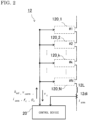
- FIG. 2 shows a schematic configuration of an arm 12 (when the arms are collectively mentioned or when any of the arms is mentioned, the arm(s) is referred to as arm 12).
- the arm 12 is one of six arms shown in FIG. 1 .
- the arm 12 includes N unit converter groups 120_1, ..., 120_k, ..., 120_N (N is an integer not less than 2) (when the unit converter groups are collectively mentioned, they are referred to as unit converter groups 120), a reactor 12L connected in series to the unit converter groups 120, and a current sensor 12di for detecting current i arm in the arm.
- N is an integer not less than 2
- the unit converter groups when the unit converter groups are collectively mentioned, they are referred to as unit converter groups 120, they are referred to as unit converter groups 120, a reactor 12L connected in series to the unit converter groups 120, and a current sensor 12di for detecting current i arm in the arm.
- one end of the unit converter group 120_1 is connected to the positive-side DC terminal 6P, and another end is connected to the unit converter group 120_2.
- One end of the unit converter group 120_N is connected to the unit converter group 120_N - 1, and another end is connected to the connection point u via the reactor 12L and the current sensor 12
- a voltage value vc of a capacitor of a unit converter included in the unit converter group 120 described later or a sum ⁇ vc of capacitor voltage values of unit converters in the unit converter group 120, and a turn-on signal for a bypass switch provided in the unit converter group 120 described later, are transmitted from the unit converter group 120 to the control device 20.
- An arm modulation command k ref , a capacitor voltage average value vc arm in the arm, an arm current detection value i arm , a carrier wave reference phase ⁇ c, and a carrier wave frequency fc are transmitted from the control device 20 to the unit converter group 120.
- FIG. 3 is a circuit diagram showing an example of the configuration of the unit converter.
- the unit converter includes a series body having semiconductor switching elements SWp, SWn connected in series as an example of switching elements, and a DC capacitor as an energy storage element connected in parallel to the series body.
- the unit converter further includes a voltage sensor for detecting the voltage vc of the DC capacitor described later, and a gate driver for performing ON/OFF control of the P-side semiconductor switching element SWp and the N-side semiconductor switching element SWn.
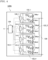
- FIG. 4 to FIG. 6 are configuration diagrams showing examples of the unit converter groups composing the arm.
- a number M of the unit converters in the unit converter group is 4 (M is an integer not less than 2).
- a unit converter group 120A includes four unit converters 122_1, 122_2, 122_3, 122_4 (when the unit converters are collectively mentioned, they are referred to as unit converters 122) connected in series, and the unit converters 122 include voltage sensors 124_1, 124_2, 124_3, 124_4 (when the voltage sensors are collectively mentioned, they are referred to as voltage sensors 124) for detecting voltages vci of their respective capacitors (i is an integer from 1 to M; here, M is 4 and vci is voltage of the capacitor that the ith unit converter has).
- the unit converter group 120A includes a gate control section 126 which receives the voltages vci of the capacitors detected by the respective voltage sensors 124 and generates gate signals for driving the semiconductor switching elements SWpi, SWni that the unit converters 122 have.
- One gate control section 126 is provided for each unit converter group.
- An AC terminal of the unit converter 122_1 located at one end in the unit converter group 120A is one terminal of the unit converter group 120A.
- An N terminal of the unit converter 122_1 is connected to an AC terminal of the unit converter 122_2, an N terminal of the unit converter 122_2 is connected to an AC terminal of the unit converter 122_3, and an N terminal of the unit converter 122_3 is connected to an AC terminal of the unit converter 122_4.
- An N terminal of the unit converter 122_4 located at another end in the unit converter group 120A is another terminal of the unit converter group 120A.
- a bypass switch 128 is provided between the terminals of the unit converter group 120A, i.e., between the AC terminal of the unit converter 122_1 and the N terminal of the unit converter 122_4. For example, in a case where the unit converter group 120A has failed, the bypass switch 128 is turned on (closed), so that current does not flow through the unit converter group 120A and thus the unit converter group 120A can be separated from the power conversion
- Gate drivers GDpi, GDni are provided for the semiconductor switching elements SWpi, SWni of the unit converter 122_i, and receive gate signals giP, giN transmitted from the gate control section 126, to perform ON/OFF control of the semiconductor switching elements SWpi, SWni. Through ON/OFF control, voltage outputted from the unit converter 122_i becomes the capacitor voltage vci or 0.
- FIG. 5 reference characters of the unit converters are not shown, but four unit converters 122_1, 122_2, 122_3, 122_4 are connected in series also in FIG. 5 . Difference from the configuration in FIG. 4 is connection parts between the unit converters.
- a P terminal of the unit converter 122_1 located at one end in a unit converter group 120B is one terminal of the unit converter group 120B.
- An AC terminal of the unit converter 122_1 is connected to a P terminal of the unit converter 122_2, an AC terminal of the unit converter 122_2 is connected to a P terminal of the unit converter 122_3, and an AC terminal of the unit converter 122_3 is connected to a P terminal of the unit converter 122_4.
- An AC terminal of the unit converter 122_4 located at another end in the unit converter group 120B is another terminal of the unit converter group 120B.
- a bypass switch 128 is provided between the terminals of the unit converter group 120B, i.e., between the P terminal of the unit converter 122_1 and the AC terminal of the unit converter 122_4.
- an AC terminal of the unit converter 122_1 located at one end in a unit converter group 120C is one terminal of the unit converter group 120C.
- An N terminal of the unit converter 122_1 is connected to a P terminal of the unit converter 122_2
- an AC terminal of the unit converter 122_2 is connected to an AC terminal of the unit converter 122_3
- an N terminal of the unit converter 122_3 is connected to a P terminal of the unit converter 122_4.
- An AC terminal of the unit converter 122_4 located at another end in the unit converter group 120C is another terminal of the unit converter group 120C.
- a bypass switch 128 is provided between the terminals of the unit converter group 120, i.e., between the AC terminal of the unit converter 122_1 and the AC terminal of the unit converter 122_4.
- Each unit converter group 120_k composing the arm 12 shown in FIG. 2 is any of the unit converter groups A, B, C shown in FIG. 4 to FIG. 6 , and it is desirable that the same kind and the same number of unit converter groups are provided in the arms 12 and in the power conversion device.
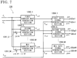
- FIG. 7 is a function block diagram showing the configuration of the gate control section 126 according to embodiment 1.
- the gate control section 126 includes M gate signal generation sections 1264 respectively corresponding to the M unit converters 122 in the unit converter group (each gate signal generation section is referred to as a gate signal generation section 1264_i, and when the gate signal generation sections are collectively mentioned, they are referred to as gate signal generation sections 1264), and carrier wave generation sections 1262 which generate carrier waves for generating gate signals (each carrier wave generation section is referred to as a carrier wave generation section 1262_i, and when the carrier wave generation sections are collectively mentioned, they are referred to as carrier wave generation sections 1262).
- the ith gate signal generation section 1264_i generates gate signals giP, giN to be transmitted to the gate drivers GDpi, GDni of the ith unit converter 122_i, and the ith carrier wave generation section 1262_i transmits a triangular carrier wave k car i to the ith gate signal generation section 1264_i.
- the ith carrier wave generation section 1262_i generates the triangular carrier wave k car i on the basis of the carrier wave frequency fc and the carrier wave reference phase ⁇ c received from the control device 20.
- Adders 1261 are provided at stages before the second carrier wave generation section 1262_2 to the Mth carrier wave generation section 1262_M.
- the second carrier wave generation section 1262_2 receives a carrier wave reference phase ⁇ c + 2 ⁇ /M through the adder 1261_2, and thus generates a triangular carrier wave k car 2 with a phase delayed by 2 ⁇ /M from the first carrier wave generation section 1262_1. Sequentially, the triangular carrier waves k car i with phases each shifted by 2 ⁇ /M are generated.
- phase shift generation of carrier waves with phases each shifted by 2 ⁇ /M is referred to as phase shift.
- the ith gate signal generation section 1264_i compares the arm modulation command k ref received from the control device 20 and the triangular carrier wave k car i received from the ith carrier wave generation section 1262_i, and outputs the gate signals giP, giN to the respective gate drivers GDpi, GDni so that, if the arm modulation command k ref is greater, voltage outputted from the ith unit converter 122_i becomes the capacitor voltage vci, and if the arm modulation command k ref is smaller, voltage outputted from the ith unit converter 122_i becomes 0.
- the ith gate signal generation section 1264_i compares the arm modulation command k ref received from the control device 20 and the triangular carrier wave k car i received from the ith carrier wave generation section 1262_i. Then, the ith gate signal generation section 1264_i outputs the gate signal giP to the gate driver GDpi so as to turn on the P-side semiconductor switching element of the ith unit converter 122_i if the arm modulation command k ref is greater.
- the ith gate signal generation section 1264_i outputs the gate signal giN to the gate driver GDni so as to turn on the N-side semiconductor switching element of the ith unit converter 122_i if the arm modulation command k ref is smaller.
- the ith gate signal generation section 1264_i compares the arm modulation command k ref received from the control device 20 and the triangular carrier wave k car i received from the ith carrier wave generation section 1262_i. Then, the ith gate signal generation section 1264_i outputs the gate signal giN to the gate driver GDni so as to turn on the N-side semiconductor switching element of the ith unit converter 122_i if the arm modulation command k ref is greater.
- the ith gate signal generation section 1264_i outputs the gate signal giP to the gate driver GDpi so as to turn on the P-side semiconductor switching element of the ith unit converter 122_i if the arm modulation command k ref is smaller.
- the gate control section 126 shown in FIG. 7 is configured under the premise that variations in the capacitor voltages vci of the unit converters 122 included in the unit converter group 120 are small, and outputs gate signals generated using the arm modulation command k ref , to the unit converters 122.
- the arm modulation command k ref is corrected using the arm current detection value i arm and a deviation between the capacitor voltage vci and a capacitor voltage average value vc arm in the arm so that the capacitor voltage vci becomes close to the capacitor voltage average value vc arm in the arm, and the corrected command is outputted as a modulation command k ref i for each unit converter to the gate signal generation section 1264_i.
- FIG. 8 is a function block diagram showing another configuration of the gate control section 126 according to embodiment 1.
- the gate control section 126 further includes balance control sections 1266.
- the ith balance control section 1266_i receives the arm modulation command k ref transmitted from the control device 20, the capacitor voltage average value vc arm in the arm, the arm current detection value i arm , and the capacitor voltage vci received from the unit converter 122_i. Then, the ith balance control section 1266_i calculates a modulation command balance correction amount corresponding to the unit converter so that the capacitor voltage vci becomes close to the capacitor voltage average value vc arm in the arm, and adds the modulation command balance correction amount to the arm modulation command k ref .
- the corrected arm modulation command is transmitted as the modulation command k ref i for the unit converter to the ith gate signal generation section 1264_i.
- the balance control sections 1266 whose number is equal to the number of the unit converters 122 are provided correspondingly to the unit converters 122 in the unit converter group 120.
- the ith gate signal generation section 1264_i compares the modulation command k ref i transmitted from the ith balance control section 1266_i and the triangular carrier wave k car i transmitted from the ith carrier wave generation section 1262_i. In the same manner as described in FIG. 7 , the ith gate signal generation section 1264_i outputs the gate signals giP, giN to the gate drivers GDpi, GDni so that, if the arm modulation command k ref is greater, voltage outputted from the ith unit converter 122_i becomes the capacitor voltage vci, and if the arm modulation command k ref is smaller, voltage outputted from the ith unit converter 122_i becomes 0.
- the control device 20 sends data of the arm modulation command k ref , the arm current detection value i arm , and the capacitor voltage average value vc arm in the arm, for each unit converter group 120.
- the transmission data amount can be reduced as compared to the conventional case. That is, the data amount can be significantly reduced as compared to a case of transmitting data for each of gate drivers of unit converters.
- phase shift of the carrier wave to be inputted to the gate signal generation section 1264 will be described.
- the number M of the unit converters in the unit converter group 120 is determined in advance and does not change during operation of the power conversion device. Therefore, a value of 2 ⁇ /M [rad] is stored in the gate control section 126 in advance, and each carrier wave generation section 1262 can generate a reference phase for the carrier wave on the basis of the carrier wave reference phase ⁇ c received from the control device 20.
- 2 ⁇ /M is a value obtained by dividing one cycle (2 ⁇ ) of the carrier wave by the number M of the unit converters in the unit converter group 120, i.e., ⁇ /M is a value obtained by equally dividing one cycle (2 ⁇ ) of the carrier wave by the number M of the unit converters in the unit converter group 120.
- FIG. 9 is a waveform diagram of the triangular carrier waves k car i and illustrates phase shift of the carrier waves in a case where the number M of the unit converters in the unit converter group is 4.
- each ith carrier wave generation section 1262_i generates the triangular carrier wave k car i on the basis of the carrier wave frequency fc and the carrier wave reference phase ⁇ c received from the control device 20, and a phase difference ⁇ a among the triangular carrier waves k car i is 2 ⁇ /M.
- each triangular carrier wave k car i having a different phase since a value of 2 ⁇ /M [rad] is stored in the gate control section 126 in advance on the basis of the number M of the unit converters in the unit converter group 120, each carrier wave generation section 1262 can easily generate a reference phase for the carrier wave on the basis of the carrier wave reference phase ⁇ c received from the control device 20. Thus, the amount of data transmitted from the control device 20 can be reduced.
- FIG. 10 is a waveform diagram of the triangular carrier waves k car i and illustrates phase shift of the carrier waves in a case where the number N of the unit converter groups in the arm 12 is 3.
- Each unit converter group includes four unit converters, as in FIG. 9 . From the top, waveforms of the triangular carrier waves k car i for the first unit converter group 120_1, the second unit converter group 120_2, and the third unit converter group 120_3 are shown. Focusing on the waveforms of the triangular carrier waves k car 1 generated by the first carrier wave generation sections in the respective unit converter groups, a phase difference among the unit converter groups is ⁇ b.
- the phase shift amount among the unit converter groups is changed in consideration of the number of the unit converter groups for which the bypass switches 128 are turned on. That is, in a case where the bypass switch 128 is turned on in one unit converter group, ⁇ b can be easily changed to a new value as ⁇ a/(N - 1). At this time, the first phase shift amount ⁇ a in the unit converter group need not be changed, and therefore the number of data to be changed can be reduced.
- the power conversion device is configured as the MMC including: the power converter 10 that includes a plurality of arms each having a plurality of (N) unit converter groups 120 which are connected in series and in each of which a plurality of (M) unit converters 122 are connected and the gate control section 126 is provided; and the control device 20 which controls the power converter 10.
- Phases for the triangular carrier waves k car i as references for generating gate signals for performing ON/OFF control of the semiconductor switching elements of the unit converters 122 are generated so as to be all shifted from each other among the semiconductor switching elements of the plurality of unit converters 122 composing each arm.
- voltage and current with reduced harmonic distortion can be outputted.
- the carrier wave generation sections 1262 of the gate control section 126 can easily generate reference phases sequentially shifted by 2 ⁇ /M on the basis of the carrier wave reference phase ⁇ c received from the control device 20, and the triangular carrier waves k car i having phases shifted from each other by 2 ⁇ /M are sequentially transmitted to the gate signal generation sections 1264.
- reference phases shifted from each other by a phase obtained by dividing 2 ⁇ /M by the number N of the unit converter groups are generated.
- the control device 20 transmits the carrier wave reference phase ⁇ c for each phase, and on the basis of the transmitted carrier wave reference phase ⁇ c, triangular carrier waves having different phases can be generated for the unit converters in the arm via a small number of signals, using the number M of the unit converters 122 and the number N of the unit converter groups 120 which are determined in advance.
- the control device 20 transmits the carrier wave reference phase ⁇ c for each phase, and on the basis of the transmitted carrier wave reference phase ⁇ c, triangular carrier waves having different phases can be generated for the unit converters in the arm via a small number of signals, using the number M of the unit converters 122 and the number N of the unit converter groups 120 which are determined in advance.
- Decrease in the number of signals is not limited to that for the carrier wave reference phase ⁇ c. Since the gate control section 126 is provided for each unit converter group 120, it suffices that the control device 20 sends data of the arm modulation command k ref , the arm current detection value i arm , and the capacitor voltage average value vc arm in the arm, for each unit converter group 120. Thus, the transmission data amount can be reduced as compared to the conventional case. That is, the data amount can be significantly reduced as compared to a case of transmitting data for each of gate drivers of unit converters, and occurrence of delay of data and the like can be suppressed.
- the gate control section 126 is provided for each unit converter group 120, it is possible to perform maintenance and a test for each unit converter group 120.
- the carrier waves are triangular waves.
- the carrier waves are not limited to triangular waves and may be saw-tooth waves or the like.
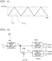
- FIG. 11 is a waveform diagram of the triangular carrier waves k car i and illustrates phase shift of carrier waves in a case where the number of the unit converters in the unit converter group 120 is 2.
- FIG. 11 corresponds to a case where M is set at 2 in FIG. 9 .
- the two carrier waves are triangular carrier waves with phases shifted from each other by 180° ( ⁇ ) which is a half cycle. Therefore, the second carrier wave k car 2 can be generated by subtracting the value of the first carrier wave k cal 1 from a top value CarTop of the triangular carrier wave.
- FIG. 12 shows the configuration of the gate control section 126 in the unit converter group 120 in the power conversion device according to embodiment 2.
- two carrier wave generation sections whose number is equal to the number M of the unit converters are not provided in the unit converter group, and it suffices that one carrier wave generation section 1262 is provided.
- the carrier wave generation section 1262 generates the triangular carrier wave k car 1 on the basis of the carrier wave frequency fc and the carrier wave reference phase ⁇ c transmitted from the control device 20.
- the generated triangular carrier wave k car 1 is transmitted to the first gate signal generation section 1264_1 and is inputted to an adder 1268 so as to be subtracted from the top value CarTop of the triangular carrier wave.
- the triangular carrier wave k car 2 outputted from the adder 1268 has a phase shifted by 180° from the triangular carrier wave k car 1, and is transmitted to the second gate signal generation section 1264_2.
- the arm modulation command k ref is corrected using the arm current detection value i arm and a deviation between the capacitor voltage vci and a capacitor voltage average value vc arm in the arm so that the capacitor voltage vci becomes close to the capacitor voltage average value vc arm in the arm, and the corrected command is outputted as a modulation command k ref i for each unit converter to the gate signal generation section 1264_i. That is, also in FIG. 12 , a configuration having the balance control section 1266 as in FIG. 8 may be adopted.
- an N terminal of the unit converter 122_1 is connected to a P terminal of the unit converter 122_2, as indicated by a broken-line elliptic part. That is, parts that are not AC terminals share a common potential, whereby the device size can be reduced.
- the other configurations are the same as those in FIG. 4 to FIG. 6 in embodiment 1 and therefore the description thereof is omitted.
- FIG. 14 shows an example of a hardware configuration of the control device 20 according to each of embodiments 1 and 2 described above.
- the control device 20 includes a processor 1000 and a storage device 1100 as processing circuits, for example.
- the processor 1000 may be formed by a central processing unit (CPU), an application specific integrated circuit (ASIC), an integrated circuit (IC), a field programmable gate array (FPGA), various logic circuits, various signal processing circuits, and the like.
- a plurality of processors 1000 that are the same type or different types may be provided and may execute processing in a shared manner.
- the storage device 1100 includes a random access memory (RAM) that allows data to be read or written from the processor 1000, and a read only memory (ROM) that allows data to be read from the processor 1000.
- the processor 1000 executes a program inputted from the storage device 1100 such as a ROM.
Landscapes
- Engineering & Computer Science (AREA)
- Power Engineering (AREA)
- Inverter Devices (AREA)
- Electric Propulsion And Braking For Vehicles (AREA)
Abstract
Description
- The present disclosure relates to a power conversion device.
- As a voltage-sourced power conversion device used in a DC power transmission system, there is known a modular multilevel converter. The modular multilevel converter is used for conversion from three-phase AC to DC or conversion opposite thereto. The modular multilevel converter includes a plurality of sub modules in each of which a plurality of cells having capacitors and switching elements are connected in series. If large amounts of harmonic components are included in voltage and current of an AC voltage grid to which the modular multilevel converter is connected, voltage balance among the capacitors is lost and waveform distortion of synthesized AC voltage increases.
- In this regard, the following technology is known. On the basis of phase information of a plurality of cells and unique information of each cell, a carrier wave for controlling ON/OFF operation of a switching element in each cell is generated, and the switching elements of the cells composing each sub module perform ON/OFF operations by carrier waves having different phases (see, for example, Patent Document 1).
- In the technology disclosed in
Patent Document 1, for the cells in one sub module in which the plurality of cells are connected in series, ON/OFF operations are performed on the basis of carrier waves having different phases, whereby waveform distortion can be reduced. In addition, since it is only necessary to generate carrier waves with phases shifted from each other, the configuration of a control device can be simplified, thus contributing to device size reduction. - Patent Document 1:
Japanese Laid-Open Patent Publication No. 2019-75844 - Meanwhile, for adapting to large-capacity power conversion, there is known a modular multilevel converter configured such that cell groups having cells connected in series are included in each sub module. In
Patent Document 1, a carrier wave is generated for each cell group in one sub module, and carrier waves having different phases are transmitted to a plurality of cell groups in one sub module (seeembodiment 3 in Patent Document 1). The carrier waves for the cells in each cell group are all equal and thus the data amount is reduced. However, since carrier waves having equal phases are present in one sub module, switching elements operating by the carrier waves having equal phases might increase harmonic distortion. In order to solve this problem, it is conceivable that carrier waves with phases shifted from each other are generated for the cells in the sub module, but such a method causes increase in the data amount of carrier waves, increase in the calculation amount, and the like, resulting in size increase of the control device. - The present disclosure has been made to solve the above problem, and an object of the present disclosure is to provide a power conversion device that includes a modular multilevel converter adaptable to large-capacity power conversion and can output voltage and current with reduced harmonic distortion, using a simple configuration, without size increase of a control device.
- A power conversion device according to the present disclosure includes: a power converter including a plurality of arms each having a plurality of unit converter groups connected in series, each unit converter group having a plurality of unit converters connected to each other; and a control device which controls the power converter. Each unit converter includes a series body having two switching elements connected in series, and a capacitor connected in parallel to the series body. Each unit converter group includes a gate control section which generates gate signals for performing ON/OFF control of a plurality of the switching elements in the unit converter group. The gate control section includes a carrier wave generation section which generates a plurality of carrier waves corresponding to a number of the unit converters in the unit converter group, and a gate signal generation section which compares a modulation command received from the control device and each carrier wave generated by the carrier wave generation section, and generates the gate signals on the basis of a result of the comparison. The plurality of carrier waves to be generated by the carrier wave generation section are generated such that phases thereof are each shifted by a first phase shift amount which is a value obtained by equally dividing one cycle of the carrier waves by the number of the unit converters in the unit converter group, using a carrier wave reference phase received from the control device as a reference, and among the unit converter groups in each arm, the phases are each shifted by a second phase shift amount which is a value obtained by equally dividing the first phase shift amount by a number of the unit converter groups in the arm, using the carrier wave reference phase received from the control device as a reference.
- The power conversion device according to the present disclosure can output voltage and current with reduced harmonic distortion, using a simple configuration, without size increase of a control device.
-
- [
FIG. 1] FIG. 1 is a schematic diagram showing the configuration of a power conversion device according toembodiment 1. - [
FIG. 2] FIG. 2 is a schematic configuration diagram of one arm composing the power conversion device according toembodiment 1. - [
FIG. 3] FIG. 3 shows the configuration of a unit converter. - [
FIG. 4] FIG. 4 is a configuration diagram showing an example of a unit converter group composing an arm. - [
FIG. 5] FIG. 5 is another configuration diagram showing an example of a unit converter group composing an arm. - [
FIG. 6] FIG. 6 is still another configuration diagram showing an example of a unit converter group composing an arm. - [
FIG. 7] FIG. 7 shows the configuration of a gate control section that the unit converter group has. - [
FIG. 8] FIG. 8 shows another configuration of a gate control section that the unit converter group has. - [
FIG. 9] FIG. 9 illustrates phase shift of carrier waves in the unit converter group. - [
FIG. 10] FIG. 10 illustrates phase shift of carrier waves among the unit converter groups in one arm. - [
FIG. 11] FIG. 11 illustrates carrier waves in a power conversion device according toembodiment 2. - [
FIG. 12] FIG. 12 shows the configuration of a gate control section according toembodiment 2. - [
FIG. 13] FIG. 13 is a configuration diagram showing an example of a unit converter group composing an arm according toembodiment 2. - [
FIG. 14] FIG. 14 is a hardware configuration diagram showing an example of the control device and the gate control section according to each embodiment. - Hereinafter, embodiments will be described with reference to the drawings. In the drawings, the same reference characters denote the same or corresponding parts.
- Hereinafter, with reference the drawings, embodiments of the present disclosure will be described in detail.
- Hereinafter, a power conversion device according to
embodiment 1 will be described with reference to the drawings. -
FIG. 1 shows a schematic configuration of a power conversion device called a modular multilevel converter (MMC) according toembodiment 1. InFIG. 1 , the power conversion device includes apower converter 10 and acontrol device 20 which controls thepower converter 10, and performs power conversion between AC and DC. Thepower converter 10 is connected between anAC power supply 1 which is a three-phase AC grid and a power device, a DC power supply, another power converter, or the like which is supplied with DC power via a positive-side DC terminal 6P and a negative-side DC terminal 6N as a DC grid. The power device, the DC power supply, the other power converter, or the like which is supplied with DC power, is not shown. Acurrent sensor 2, avoltage sensor 3, atransformer 4, and the like are connected between theAC power supply 1 and thepower converter 10, and AC current Iac detected by thecurrent sensor 2 and AC voltage Vac detected by thevoltage sensor 3 are outputted to thecontrol device 20.Voltage sensors 14p, 14n for detecting DC voltage Vdc are provided to the DC grid. - The
power converter 10 has three leg circuits corresponding to u phase, v phase, and w phase of the three-phase AC, and the three leg circuits are connected in parallel between the positive-side DC terminal 6P and the negative-side DC terminal 6N. - The leg circuit for u phase is formed of a positive-side u-phase arm 12pu and a negative-side u-phase arm 12nu connected in series. One end of the positive-side u-phase arm 12pu is connected to the positive-
side DC terminal 6P, one end of the negative-side u-phase arm 12nu is connected to the negative-side DC terminal 6N, and a connection point u between the positive-side u-phase arm 12pu and the negative-side u-phase arm 12nu is connected to a u-phase terminal of thetransformer 4. - The leg circuit for v phase is formed of a positive-side v-phase arm 12pv and a negative-side v-phase arm 12nv connected in series. One end of the positive-side v-phase arm 12pv is connected to the positive-
side DC terminal 6P, one end of the negative-side v-phase arm 12nv is connected to the negative-side DC terminal 6N, and a connection point v between the positive-side v-phase arm 12pv and the negative-side v-phase arm 12nv is connected to a v-phase terminal of thetransformer 4. - The leg circuit for w phase is formed of a positive-side w-phase arm 12pw and a negative-side w-phase arm 12nw connected in series. One end of the positive-side w-phase arm 12pw is connected to the positive-
side DC terminal 6P, one end of the negative-side w-phase arm 12nw is connected to the negative-side DC terminal 6N, and a connection point w between the positive-side w-phase arm 12pw and the negative-side w-phase arm 12nw is connected to a w-phase terminal of thetransformer 4. - Next, the configuration of each arm of the
power converter 10 will be described with reference toFIG. 2 . -
FIG. 2 shows a schematic configuration of an arm 12 (when the arms are collectively mentioned or when any of the arms is mentioned, the arm(s) is referred to as arm 12). In the drawing, thearm 12 is one of six arms shown inFIG. 1 . - In
FIG. 2 , thearm 12 includes N unit converter groups 120_1, ..., 120_k, ..., 120_N (N is an integer not less than 2) (when the unit converter groups are collectively mentioned, they are referred to as unit converter groups 120), areactor 12L connected in series to theunit converter groups 120, and a current sensor 12di for detecting current iarm in the arm. In a case where thearm 12 is the positive-side u-phase arm 12pu inFIG. 1 , one end of the unit converter group 120_1 is connected to the positive-side DC terminal 6P, and another end is connected to the unit converter group 120_2. One end of the unit converter group 120_N is connected to the unit converter group 120_N - 1, and another end is connected to the connection point u via thereactor 12L and the current sensor 12di for detecting the current iarm in the arm. - A voltage value vc of a capacitor of a unit converter included in the
unit converter group 120 described later or a sum Σvc of capacitor voltage values of unit converters in theunit converter group 120, and a turn-on signal for a bypass switch provided in theunit converter group 120 described later, are transmitted from theunit converter group 120 to thecontrol device 20. - An arm modulation command kref, a capacitor voltage average value vcarm in the arm, an arm current detection value iarm, a carrier wave reference phase θc, and a carrier wave frequency fc are transmitted from the
control device 20 to theunit converter group 120. - Next, the configuration of the unit converter included in the
unit converter group 120 will be described with reference toFIG. 3 . -
FIG. 3 is a circuit diagram showing an example of the configuration of the unit converter. The unit converter includes a series body having semiconductor switching elements SWp, SWn connected in series as an example of switching elements, and a DC capacitor as an energy storage element connected in parallel to the series body. Although not shown, the unit converter further includes a voltage sensor for detecting the voltage vc of the DC capacitor described later, and a gate driver for performing ON/OFF control of the P-side semiconductor switching element SWp and the N-side semiconductor switching element SWn. - Next, the configuration of the
unit converter group 120 will be described with reference toFIG. 4 to FIG. 6 . -
FIG. 4 to FIG. 6 are configuration diagrams showing examples of the unit converter groups composing the arm. In these examples, a number M of the unit converters in the unit converter group is 4 (M is an integer not less than 2). - In
FIG. 4 , aunit converter group 120A includes four unit converters 122_1, 122_2, 122_3, 122_4 (when the unit converters are collectively mentioned, they are referred to as unit converters 122) connected in series, and theunit converters 122 include voltage sensors 124_1, 124_2, 124_3, 124_4 (when the voltage sensors are collectively mentioned, they are referred to as voltage sensors 124) for detecting voltages vci of their respective capacitors (i is an integer from 1 to M; here, M is 4 and vci is voltage of the capacitor that the ith unit converter has). Theunit converter group 120A includes agate control section 126 which receives the voltages vci of the capacitors detected by therespective voltage sensors 124 and generates gate signals for driving the semiconductor switching elements SWpi, SWni that theunit converters 122 have. Onegate control section 126 is provided for each unit converter group. - An AC terminal of the unit converter 122_1 located at one end in the
unit converter group 120A is one terminal of theunit converter group 120A. An N terminal of the unit converter 122_1 is connected to an AC terminal of the unit converter 122_2, an N terminal of the unit converter 122_2 is connected to an AC terminal of the unit converter 122_3, and an N terminal of the unit converter 122_3 is connected to an AC terminal of the unit converter 122_4. An N terminal of the unit converter 122_4 located at another end in theunit converter group 120A is another terminal of theunit converter group 120A. Abypass switch 128 is provided between the terminals of theunit converter group 120A, i.e., between the AC terminal of the unit converter 122_1 and the N terminal of the unit converter 122_4. For example, in a case where theunit converter group 120A has failed, thebypass switch 128 is turned on (closed), so that current does not flow through theunit converter group 120A and thus theunit converter group 120A can be separated from the power conversion device. - Gate drivers GDpi, GDni are provided for the semiconductor switching elements SWpi, SWni of the unit converter 122_i, and receive gate signals giP, giN transmitted from the
gate control section 126, to perform ON/OFF control of the semiconductor switching elements SWpi, SWni. Through ON/OFF control, voltage outputted from the unit converter 122_i becomes the capacitor voltage vci or 0. - In
FIG. 5 , reference characters of the unit converters are not shown, but four unit converters 122_1, 122_2, 122_3, 122_4 are connected in series also inFIG. 5 . Difference from the configuration inFIG. 4 is connection parts between the unit converters. InFIG. 5 , a P terminal of the unit converter 122_1 located at one end in aunit converter group 120B is one terminal of theunit converter group 120B. An AC terminal of the unit converter 122_1 is connected to a P terminal of the unit converter 122_2, an AC terminal of the unit converter 122_2 is connected to a P terminal of the unit converter 122_3, and an AC terminal of the unit converter 122_3 is connected to a P terminal of the unit converter 122_4. An AC terminal of the unit converter 122_4 located at another end in theunit converter group 120B is another terminal of theunit converter group 120B. As inFIG. 4 , abypass switch 128 is provided between the terminals of theunit converter group 120B, i.e., between the P terminal of the unit converter 122_1 and the AC terminal of the unit converter 122_4. - In
FIG. 6 , difference from the configurations inFIG. 4 andFIG. 5 is connection parts between the unit converters. InFIG. 6 , an AC terminal of the unit converter 122_1 located at one end in aunit converter group 120C is one terminal of theunit converter group 120C. An N terminal of the unit converter 122_1 is connected to a P terminal of the unit converter 122_2, an AC terminal of the unit converter 122_2 is connected to an AC terminal of the unit converter 122_3, and an N terminal of the unit converter 122_3 is connected to a P terminal of the unit converter 122_4. An AC terminal of the unit converter 122_4 located at another end in theunit converter group 120C is another terminal of theunit converter group 120C. As inFIG. 4 andFIG. 5 , abypass switch 128 is provided between the terminals of theunit converter group 120, i.e., between the AC terminal of the unit converter 122_1 and the AC terminal of the unit converter 122_4. - Each unit converter group 120_k composing the
arm 12 shown inFIG. 2 is any of the unit converter groups A, B, C shown inFIG. 4 to FIG. 6 , and it is desirable that the same kind and the same number of unit converter groups are provided in thearms 12 and in the power conversion device. - Next, the
gate control section 126 included in theunit converter group 120 will be described. -
FIG. 7 is a function block diagram showing the configuration of thegate control section 126 according toembodiment 1. Thegate control section 126 includes M gatesignal generation sections 1264 respectively corresponding to theM unit converters 122 in the unit converter group (each gate signal generation section is referred to as a gate signal generation section 1264_i, and when the gate signal generation sections are collectively mentioned, they are referred to as gate signal generation sections 1264), and carrierwave generation sections 1262 which generate carrier waves for generating gate signals (each carrier wave generation section is referred to as a carrier wave generation section 1262_i, and when the carrier wave generation sections are collectively mentioned, they are referred to as carrier wave generation sections 1262). The ith gate signal generation section 1264_i generates gate signals giP, giN to be transmitted to the gate drivers GDpi, GDni of the ith unit converter 122_i, and the ith carrier wave generation section 1262_i transmits a triangular carrier wave kcari to the ith gate signal generation section 1264_i. - The ith carrier wave generation section 1262_i generates the triangular carrier wave kcari on the basis of the carrier wave frequency fc and the carrier wave reference phase θc received from the
control device 20. Adders 1261 are provided at stages before the second carrier wave generation section 1262_2 to the Mth carrier wave generation section 1262_M. The second carrier wave generation section 1262_2 receives a carrier wave reference phase θc + 2π/M through the adder 1261_2, and thus generates a triangularcarrier wave k car2 with a phase delayed by 2π/M from the first carrier wave generation section 1262_1. Sequentially, the triangular carrier waves kcari with phases each shifted by 2π/M are generated. That is, the triangular carrier waves kcari with phases all different from each other are transmitted to theM unit converters 122 in theunit converter group 120. Hereinafter, generation of carrier waves with phases each shifted by 2π/M is referred to as phase shift. - The ith gate signal generation section 1264_i compares the arm modulation command kref received from the
control device 20 and the triangular carrier wave kcari received from the ith carrier wave generation section 1262_i, and outputs the gate signals giP, giN to the respective gate drivers GDpi, GDni so that, if the arm modulation command kref is greater, voltage outputted from the ith unit converter 122_i becomes the capacitor voltage vci, and if the arm modulation command kref is smaller, voltage outputted from the ith unit converter 122_i becomes 0. - That is, for the unit converters 122_1, 122_2, 122_3, 122_4 in the
unit converter group 120A shown inFIG. 4 and the unit converters 122_1, 122_3 in theunit converter group 120C shown inFIG. 6 , the ith gate signal generation section 1264_i compares the arm modulation command kref received from thecontrol device 20 and the triangular carrier wave kcari received from the ith carrier wave generation section 1262_i. Then, the ith gate signal generation section 1264_i outputs the gate signal giP to the gate driver GDpi so as to turn on the P-side semiconductor switching element of the ith unit converter 122_i if the arm modulation command kref is greater. Meanwhile, the ith gate signal generation section 1264_i outputs the gate signal giN to the gate driver GDni so as to turn on the N-side semiconductor switching element of the ith unit converter 122_i if the arm modulation command kref is smaller. - For the unit converters 122_1, 122_2, 122_3, 122_4 in the
unit converter group 120B shown inFIG. 5 and the unit converters 122_2, 122_4 in theunit converter group 120C shown inFIG. 6 , the ith gate signal generation section 1264_i compares the arm modulation command kref received from thecontrol device 20 and the triangular carrier wave kcari received from the ith carrier wave generation section 1262_i. Then, the ith gate signal generation section 1264_i outputs the gate signal giN to the gate driver GDni so as to turn on the N-side semiconductor switching element of the ith unit converter 122_i if the arm modulation command kref is greater. Meanwhile, the ith gate signal generation section 1264_i outputs the gate signal giP to the gate driver GDpi so as to turn on the P-side semiconductor switching element of the ith unit converter 122_i if the arm modulation command kref is smaller. - The
gate control section 126 shown inFIG. 7 is configured under the premise that variations in the capacitor voltages vci of theunit converters 122 included in theunit converter group 120 are small, and outputs gate signals generated using the arm modulation command kref, to theunit converters 122. - In a case where there are variations in the capacitor voltages vci of the
unit converters 122 included in theunit converter group 120, it is desirable that the arm modulation command kref is corrected using the arm current detection value iarm and a deviation between the capacitor voltage vci and a capacitor voltage average value vcarm in the arm so that the capacitor voltage vci becomes close to the capacitor voltage average value vcarm in the arm, and the corrected command is outputted as a modulation command krefi for each unit converter to the gate signal generation section 1264_i. -
FIG. 8 is a function block diagram showing another configuration of thegate control section 126 according toembodiment 1. InFIG. 8 , thegate control section 126 further includes balance control sections 1266. The ith balance control section 1266_i receives the arm modulation command kref transmitted from thecontrol device 20, the capacitor voltage average value vcarm in the arm, the arm current detection value iarm, and the capacitor voltage vci received from the unit converter 122_i. Then, the ith balance control section 1266_i calculates a modulation command balance correction amount corresponding to the unit converter so that the capacitor voltage vci becomes close to the capacitor voltage average value vcarm in the arm, and adds the modulation command balance correction amount to the arm modulation command kref. The corrected arm modulation command is transmitted as the modulation command krefi for the unit converter to the ith gate signal generation section 1264_i. Here, the balance control sections 1266 whose number is equal to the number of theunit converters 122 are provided correspondingly to theunit converters 122 in theunit converter group 120. - In
FIG. 8 , the ith gate signal generation section 1264_i compares the modulation command krefi transmitted from the ith balance control section 1266_i and the triangular carrier wave kcari transmitted from the ith carrier wave generation section 1262_i. In the same manner as described inFIG. 7 , the ith gate signal generation section 1264_i outputs the gate signals giP, giN to the gate drivers GDpi, GDni so that, if the arm modulation command kref is greater, voltage outputted from the ith unit converter 122_i becomes the capacitor voltage vci, and if the arm modulation command kref is smaller, voltage outputted from the ith unit converter 122_i becomes 0. - Since the
gate control section 126 is provided for eachunit converter group 120, it suffices that thecontrol device 20 sends data of the arm modulation command kref, the arm current detection value iarm, and the capacitor voltage average value vcarm in the arm, for eachunit converter group 120. Thus, the transmission data amount can be reduced as compared to the conventional case. That is, the data amount can be significantly reduced as compared to a case of transmitting data for each of gate drivers of unit converters. - Next, phase shift of the carrier wave to be inputted to the gate
signal generation section 1264 will be described. The number M of the unit converters in theunit converter group 120 is determined in advance and does not change during operation of the power conversion device. Therefore, a value of 2π/M [rad] is stored in thegate control section 126 in advance, and each carrierwave generation section 1262 can generate a reference phase for the carrier wave on the basis of the carrier wave reference phase θc received from thecontrol device 20. Here, 2π/M is a value obtained by dividing one cycle (2π) of the carrier wave by the number M of the unit converters in theunit converter group 120, i.e., π/M is a value obtained by equally dividing one cycle (2π) of the carrier wave by the number M of the unit converters in theunit converter group 120. -
FIG. 9 is a waveform diagram of the triangular carrier waves kcari and illustrates phase shift of the carrier waves in a case where the number M of the unit converters in the unit converter group is 4. InFIG. 9 , among the triangular carrier waves kcari, the triangular carrier wave generated by the first carrier wave generation section 1262_1 is denoted with i = 1, and the remaining triangular carrier waves are sequentially denoted up to i = 4. As described above, each ith carrier wave generation section 1262_i generates the triangular carrier wave kcari on the basis of the carrier wave frequency fc and the carrier wave reference phase θc received from thecontrol device 20, and a phase difference φa among the triangular carrier waves kcari is 2π/M. Regarding each triangular carrier wave kcari having a different phase, since a value of 2π/M [rad] is stored in thegate control section 126 in advance on the basis of the number M of the unit converters in theunit converter group 120, each carrierwave generation section 1262 can easily generate a reference phase for the carrier wave on the basis of the carrier wave reference phase θc received from thecontrol device 20. Thus, the amount of data transmitted from thecontrol device 20 can be reduced. - Next, phase shift of carrier waves in a case where there are three
unit converter groups 120 in the arm 12 (N = 3) will be described with reference toFIG. 10 . -
FIG. 10 is a waveform diagram of the triangular carrier waves kcari and illustrates phase shift of the carrier waves in a case where the number N of the unit converter groups in thearm 12 is 3. Each unit converter group includes four unit converters, as inFIG. 9 . From the top, waveforms of the triangular carrier waves kcari for the first unit converter group 120_1, the second unit converter group 120_2, and the third unit converter group 120_3 are shown. Focusing on the waveforms of the triangularcarrier waves k car1 generated by the first carrier wave generation sections in the respective unit converter groups, a phase difference among the unit converter groups is φb. The phase difference φb is a value obtained by dividing a first phase shift amount φa (= 2π/M [rad]) in the unit converter group by the number N of the unit converter groups in the arm, and therefore is a value obtained by equally dividing φa by N. That is, the triangular carrier wave kcari generated by the carrier wave generation section in the arm has a phase difference obtained by equally dividing 360° (= 2π) by the total number (M×N) of the unit converters in the arm. Thus, harmonics that would occur when the carrier waves have the same phase can be prevented from occurring. - The number N of the unit converter groups in the arm is determined in advance and does not change during operation of the power conversion device. Therefore, if a second phase shift amount φb (= φa/N [rad]) is stored in the
gate control section 126 together with the first phase shift amount φa (= 2π/M [rad]) in advance, each carrierwave generation section 1262 in the arm can generate a reference phase for the carrier wave on the basis of the carrier wave reference phase θc received from thecontrol device 20. Thus, the amount of data transmitted from thecontrol device 20 can be reduced. - In a case where any of the
unit converter groups 120 has failed or has become abnormal, or in a case where any of theunit converters 122 in theunit converter group 120 has failed or has become abnormal and thus thebypass switch 128 of the unit converter group including theunit converter 122 that has failed or has become abnormal is turned on, it suffices that the phase shift amount among the unit converter groups is changed in consideration of the number of the unit converter groups for which the bypass switches 128 are turned on. That is, in a case where thebypass switch 128 is turned on in one unit converter group, φb can be easily changed to a new value as φa/(N - 1). At this time, the first phase shift amount φa in the unit converter group need not be changed, and therefore the number of data to be changed can be reduced. - As described above, the power conversion device according to the
present embodiment 1 is configured as the MMC including: thepower converter 10 that includes a plurality of arms each having a plurality of (N)unit converter groups 120 which are connected in series and in each of which a plurality of (M)unit converters 122 are connected and thegate control section 126 is provided; and thecontrol device 20 which controls thepower converter 10. Phases for the triangular carrier waves kcari as references for generating gate signals for performing ON/OFF control of the semiconductor switching elements of theunit converters 122 are generated so as to be all shifted from each other among the semiconductor switching elements of the plurality ofunit converters 122 composing each arm. Thus, voltage and current with reduced harmonic distortion can be outputted. In eachunit converter group 120, the carrierwave generation sections 1262 of thegate control section 126 can easily generate reference phases sequentially shifted by 2π/M on the basis of the carrier wave reference phase θc received from thecontrol device 20, and the triangular carrier waves kcari having phases shifted from each other by 2π/M are sequentially transmitted to the gatesignal generation sections 1264. Among theunit converter groups 120, reference phases shifted from each other by a phase obtained by dividing 2π/M by the number N of the unit converter groups are generated. Therefore, thecontrol device 20 transmits the carrier wave reference phase θc for each phase, and on the basis of the transmitted carrier wave reference phase θc, triangular carrier waves having different phases can be generated for the unit converters in the arm via a small number of signals, using the number M of theunit converters 122 and the number N of theunit converter groups 120 which are determined in advance. Thus, it becomes possible to output voltage and current with reduced harmonic distortion, using a simple configuration, without size increase of thecontrol device 20. - Decrease in the number of signals is not limited to that for the carrier wave reference phase θc. Since the
gate control section 126 is provided for eachunit converter group 120, it suffices that thecontrol device 20 sends data of the arm modulation command kref, the arm current detection value iarm, and the capacitor voltage average value vcarm in the arm, for eachunit converter group 120. Thus, the transmission data amount can be reduced as compared to the conventional case. That is, the data amount can be significantly reduced as compared to a case of transmitting data for each of gate drivers of unit converters, and occurrence of delay of data and the like can be suppressed. - Since the
gate control section 126 is provided for eachunit converter group 120, it is possible to perform maintenance and a test for eachunit converter group 120. - In
FIG. 9 and FIG. 10 , the examples in which the carrier waves are triangular waves have been shown. However, the carrier waves are not limited to triangular waves and may be saw-tooth waves or the like. - Hereinafter, a power conversion device according to
embodiment 2 will be described with reference to the drawings. - Regarding the power conversion device according to
embodiment 2, it is assumed that the number of the unit converters included in each unit converter group is 2 (M = 2) as an example, and a carrier wave generation method and a configuration of the unit converter group different from those inembodiment 1 will be described. -
FIG. 11 is a waveform diagram of the triangular carrier waves kcari and illustrates phase shift of carrier waves in a case where the number of the unit converters in theunit converter group 120 is 2.FIG. 11 corresponds to a case where M is set at 2 inFIG. 9 . In a case where the number M of the unit converters is 2, the two carrier waves are triangular carrier waves with phases shifted from each other by 180° (π) which is a half cycle. Therefore, the secondcarrier wave k car2 can be generated by subtracting the value of the firstcarrier wave k cal1 from a top value CarTop of the triangular carrier wave. -
FIG. 12 shows the configuration of thegate control section 126 in theunit converter group 120 in the power conversion device according toembodiment 2. As compared toFIG. 7 andFIG. 8 , inFIG. 12 , two carrier wave generation sections whose number is equal to the number M of the unit converters are not provided in the unit converter group, and it suffices that one carrierwave generation section 1262 is provided. InFIG. 12 , the carrierwave generation section 1262 generates the triangularcarrier wave k car1 on the basis of the carrier wave frequency fc and the carrier wave reference phase θc transmitted from thecontrol device 20. The generated triangularcarrier wave k car1 is transmitted to the first gate signal generation section 1264_1 and is inputted to anadder 1268 so as to be subtracted from the top value CarTop of the triangular carrier wave. The triangularcarrier wave k car2 outputted from theadder 1268 has a phase shifted by 180° from the triangularcarrier wave k car1, and is transmitted to the second gate signal generation section 1264_2. - In the
present embodiment 2, in a case where there are variations in the capacitor voltages vci of theunit converters 122 of theunit converter group 120, it is desirable that the arm modulation command kref is corrected using the arm current detection value iarm and a deviation between the capacitor voltage vci and a capacitor voltage average value vcarm in the arm so that the capacitor voltage vci becomes close to the capacitor voltage average value vcarm in the arm, and the corrected command is outputted as a modulation command krefi for each unit converter to the gate signal generation section 1264_i. That is, also inFIG. 12 , a configuration having the balance control section 1266 as inFIG. 8 may be adopted. - Next, in the example in which the number of the unit converters included in the unit converter group is 2 (M = 2), a configuration of the unit converter group different from that shown in
embodiment 1 will be described with reference toFIG. 13 . - In
FIG. 13 , in aunit converter group 120D, an N terminal of the unit converter 122_1 is connected to a P terminal of the unit converter 122_2, as indicated by a broken-line elliptic part. That is, parts that are not AC terminals share a common potential, whereby the device size can be reduced. The other configurations are the same as those inFIG. 4 to FIG. 6 inembodiment 1 and therefore the description thereof is omitted. - As described above, with the power conversion device according to
embodiment 2, the effects ofembodiment 1 are provided, and in addition, in a case where the number of theunit converters 122 included in theunit converter group 120 is 2, thegate control section 126 of eachunit converter group 120 need not have two carrierwave generation sections 1262 whose number is equal to the number of theunit converters 122 but it suffices that one carrierwave generation section 1262 is provided and calculation by theadder 1268 is performed. Thus, the device configuration is simplified and the calculation amount is reduced. - In a case where the number of the unit converters included in the unit converter group is 2 (M = 2), parts that are not AC terminals can share a common potential in the configuration inside the unit converter group, leading to further device size reduction.
- Thus, it becomes possible to provide a power conversion device that has a modular multilevel converter (MMC) adaptable to large-capacity power conversion and can output voltage and current with reduced harmonic distortion, using a simple configuration, without size increase of a control device.
-
FIG. 14 shows an example of a hardware configuration of thecontrol device 20 according to each ofembodiments FIG. 14 , thecontrol device 20 includes aprocessor 1000 and astorage device 1100 as processing circuits, for example. - The
processor 1000 may be formed by a central processing unit (CPU), an application specific integrated circuit (ASIC), an integrated circuit (IC), a field programmable gate array (FPGA), various logic circuits, various signal processing circuits, and the like. A plurality ofprocessors 1000 that are the same type or different types may be provided and may execute processing in a shared manner. Thestorage device 1100 includes a random access memory (RAM) that allows data to be read or written from theprocessor 1000, and a read only memory (ROM) that allows data to be read from theprocessor 1000. Theprocessor 1000 executes a program inputted from thestorage device 1100 such as a ROM. - The
gate control section 126 also has the hardware configuration shown inFIG. 14 as in thecontrol device 20, and executes a program for generating signals for performing drive control of the gates. -
- (1) In the above description, the example in which the semiconductor switching elements SWp, SWn as the switching elements composing the
unit converter 122 are insulated gate bipolar transistors (IGBTs), has been shown. However, metal oxide semiconductor field effect transistors (MOSFETs) may be used. - (2) The semiconductor switching elements are not limited to those made of a Si (silicon) semiconductor, and may be made of a wide bandgap semiconductor such as SiC (silicon carbide) or GaN (gallium nitride). The wide bandgap semiconductor has such characteristics that allow higher-speed switching, allow high-temperature operation, and exhibit a high dielectric-breakdown electric field strength, for example, and therefore is preferably applied to the MMC.
- Although the disclosure is described above in terms of various exemplary embodiments and implementations, it should be understood that the various features, aspects, and functionality described in one or more of the individual embodiments are not limited in their applicability to the particular embodiment with which they are described, but instead can be applied, alone or in various combinations to one or more of the embodiments of the disclosure.
- It is therefore understood that numerous modifications which have not been exemplified can be devised without departing from the scope of the present disclosure. For example, at least one of the constituent components may be modified, added, or eliminated. At least one of the constituent components mentioned in at least one of the preferred embodiments may be selected and combined with the constituent components mentioned in another preferred embodiment.
-
- 1 AC power supply
- 2 current sensor
- 3 voltage sensor
- 4 transformer
- 6P positive-side DC terminal
- 6N negative-side DC terminal
- 10 power converter
- 12, 12pu, 12nu, 12pv, 12nv, 12pw, 12nw arm
- 14p, 14n voltage sensor
- 20 control device
- 12L reactor
- 12di current sensor
- 120, 120_1, 120_2, 120_3, 120_k, 120_N, 120A, 120B, 120C, 120D unit converter group
- 122, 122_1, 122_2, 122_3, 122_4, 122_i unit converter
- 124, 124_1 voltage sensor
- 126 gate control section
- 128 bypass switch
- 1261, 1261_2, 1268 adder
- 1262, 1262_1, 1262_2, 1262_i, 1262_M carrier wave generation section
- 1264, 1264_1, 1264_2, 1264_i gate signal generation section
- 1266, 1266_i balance control section
- 1000 processor
- 1100 storage device
- Vac AC voltage
- Vdc DC voltage
- Iac AC current
- vc voltage value of capacitor
- kref, krefi arm modulation command
- vcarm capacitor voltage average value in arm
- iarm arm current detection value
- θc carrier wave reference phase
- fc carrier wave frequency
-
k car1,k car2, kcari triangular carrier wave - GDpi, GDni gate driver
- giP, giN gate signal
- SWp, SWpi, SWn, SWni semiconductor switching element
- u, v, w connection point
- φa first phase shift amount
- φb second phase shift amount
Claims (6)
- A power conversion device comprising:a power converter including a plurality of arms each having a plurality of unit converter groups connected in series, each unit converter group having a plurality of unit converters connected to each other; anda control device which controls the power converter, whereineach unit converter includes a series body having two switching elements connected in series, and a capacitor connected in parallel to the series body,each unit converter group includes a gate control section which generates gate signals for performing ON/OFF control of a plurality of the switching elements in the unit converter group,the gate control section includes a carrier wave generation section which generates a plurality of carrier waves corresponding to a number of the unit converters in the unit converter group, and a gate signal generation section which compares a modulation command received from the control device and each carrier wave generated by the carrier wave generation section, and generates the gate signals on the basis of a result of the comparison, andthe plurality of carrier waves to be generated by the carrier wave generation section are generated such that phases thereof are each shifted by a first phase shift amount which is a value obtained by equally dividing one cycle of the carrier waves by the number of the unit converters in the unit converter group, using a carrier wave reference phase received from the control device as a reference, and among the unit converter groups in each arm, the phases are each shifted by a second phase shift amount which is a value obtained by equally dividing the first phase shift amount by a number of the unit converter groups in the arm, using the carrier wave reference phase received from the control device as a reference.
- The power conversion device according to claim 1, whereineach unit converter group includes one bypass switch,the bypass switch is connected between a terminal of the unit converter located at one end in the unit converter group and a terminal of the unit converter located at another end,in a case where any of the unit converters in the unit converter group has failed or has become abnormal, the bypass switch of the unit converter group including the unit converter that has failed or has become abnormal is turned on, andthe second phase shift amount is calculated using a number obtained by subtracting, from the number of the unit converter groups, a number of the unit converter groups for which the bypass switches are turned on, in the arm.
- The power conversion device according to claim 1 or 2, whereinthe unit converter group includes two said unit converters,a first carrier wave which is one of two said carrier waves generated by the carrier wave generation section is a triangular wave generated on the basis of a carrier wave frequency and the carrier wave reference phase received from the control device, anda second carrier wave which is the other carrier wave is generated by subtracting a value of the first carrier wave from a top value of the first carrier wave.
- The power conversion device according to claim 3, wherein
in the unit converter group, an N terminal of one of the two unit converters and a P terminal of the other unit converter are connected as a common terminal. - The power conversion device according to any one of claims 1 to 4, whereinthe unit converter includes a voltage sensor for detecting voltage of the capacitor of the unit converter,the gate control section further includes balance control sections whose number corresponds to a number of the unit converters included in the unit converter group,correspondingly to the respective unit converters, each of the balance control sections outputs a modulation command balance correction amount obtained by comparing the voltage of the capacitor of the unit converter and a voltage average value of the capacitors in the arm, and calculates a corrected modulation command obtained by adding the modulation command balance correction amount to the modulation command received from the control device, andthe gate signal generation section compares the corrected modulation command and each carrier wave, and outputs the gate signals on the basis of a result of the comparison.
- The power conversion device according to any one of claims 1 to 5, wherein
one said gate control section is provided for each unit converter group.
Applications Claiming Priority (1)
| Application Number | Priority Date | Filing Date | Title |
|---|---|---|---|
| PCT/JP2022/031087 WO2024038520A1 (en) | 2022-08-17 | 2022-08-17 | Power conversion device |
Publications (2)
| Publication Number | Publication Date |
|---|---|
| EP4576553A1 true EP4576553A1 (en) | 2025-06-25 |
| EP4576553A4 EP4576553A4 (en) | 2025-10-22 |
Family
ID=89941468
Family Applications (1)
| Application Number | Title | Priority Date | Filing Date |
|---|---|---|---|
| EP22955694.9A Pending EP4576553A4 (en) | 2022-08-17 | 2022-08-17 | POWER CONVERTER |
Country Status (3)
| Country | Link |
|---|---|
| EP (1) | EP4576553A4 (en) |
| JP (1) | JP7825720B2 (en) |
| WO (1) | WO2024038520A1 (en) |
Family Cites Families (5)
| Publication number | Priority date | Publication date | Assignee | Title |
|---|---|---|---|---|
| JP2000287453A (en) * | 1999-03-31 | 2000-10-13 | Mitsubishi Electric Corp | Multiple power converter |
| JP6116804B2 (en) * | 2012-02-14 | 2017-04-19 | 株式会社東芝 | Neutral point clamp type inverter |
| JP6892812B2 (en) | 2017-10-12 | 2021-06-23 | 株式会社日立製作所 | Power converter |
| JP2020080627A (en) * | 2018-11-14 | 2020-05-28 | 株式会社日立製作所 | Power conversion device and power conversion method thereof |
| US11824461B2 (en) | 2020-06-24 | 2023-11-21 | North Carolina State University | MMC submodules scale-up methodology for MV and HV power conversion system applications |
-
2022
- 2022-08-17 JP JP2024541326A patent/JP7825720B2/en active Active
- 2022-08-17 WO PCT/JP2022/031087 patent/WO2024038520A1/en not_active Ceased
- 2022-08-17 EP EP22955694.9A patent/EP4576553A4/en active Pending
Also Published As
| Publication number | Publication date |
|---|---|
| WO2024038520A1 (en) | 2024-02-22 |
| EP4576553A4 (en) | 2025-10-22 |
| JPWO2024038520A1 (en) | 2024-02-22 |
| JP7825720B2 (en) | 2026-03-06 |
Similar Documents
| Publication | Publication Date | Title |
|---|---|---|
| JP6676229B1 (en) | Power converter | |
| EP3501091B1 (en) | Modulation of ac/ac mmc | |
| US11601064B2 (en) | Power conversion device having a frequency of a first control signal higher than a frequency of a second control signal | |
| EP3273587B1 (en) | Inverter control method | |
| EP2913915A1 (en) | Power conversion device | |
| EP3637608B1 (en) | Power conversion device | |
| US12107487B2 (en) | Power conversion device | |
| EP4224696A1 (en) | Power conversion device | |
| EP4576553A1 (en) | Power conversion device | |
| US10693392B2 (en) | Power conversion device and electric motor drive device using same | |
| WO2019167244A1 (en) | Power conversion device and electric motor system | |
| JP2020167778A (en) | Control device for direct power converter | |
| CN117882287A (en) | Power converter control unit and power conversion device | |
| JP2022056359A (en) | Power conversion apparatus | |
| JP7843947B1 (en) | Power converter | |
| JP7819429B1 (en) | Power Conversion Device | |
| JP7810048B2 (en) | Power Conversion Device | |
| EP4641909A1 (en) | Power conversion device | |
| US12500528B2 (en) | Power conversion device | |
| EP4358389A1 (en) | Power conversion device and power conversion method | |
| JPH11206020A (en) | PWM controller | |
| WO2025177422A1 (en) | Power conversion device | |
| WO2023214462A1 (en) | Power conversion device | |
| Aldhandi et al. | Fault analysis of diode clamped inverter based induction motor drive |
Legal Events
| Date | Code | Title | Description |
|---|---|---|---|
| STAA | Information on the status of an ep patent application or granted ep patent |
Free format text: STATUS: THE INTERNATIONAL PUBLICATION HAS BEEN MADE |
|
| PUAI | Public reference made under article 153(3) epc to a published international application that has entered the european phase |
Free format text: ORIGINAL CODE: 0009012 |
|
| STAA | Information on the status of an ep patent application or granted ep patent |
Free format text: STATUS: REQUEST FOR EXAMINATION WAS MADE |
|
| 17P | Request for examination filed |
Effective date: 20250113 |
|
| AK | Designated contracting states |
Kind code of ref document: A1 Designated state(s): AL AT BE BG CH CY CZ DE DK EE ES FI FR GB GR HR HU IE IS IT LI LT LU LV MC MK MT NL NO PL PT RO RS SE SI SK SM TR |
|
| A4 | Supplementary search report drawn up and despatched |
Effective date: 20250919 |
|
| RIC1 | Information provided on ipc code assigned before grant |
Ipc: H02M 7/49 20070101AFI20250915BHEP Ipc: H02M 1/12 20060101ALI20250915BHEP Ipc: H02M 1/32 20070101ALI20250915BHEP Ipc: H02M 1/00 20060101ALI20250915BHEP |
|
| DAV | Request for validation of the european patent (deleted) | ||
| DAX | Request for extension of the european patent (deleted) |