EP4576541A1 - Boost and buck apparatus and system - Google Patents
Boost and buck apparatus and system Download PDFInfo
- Publication number
- EP4576541A1 EP4576541A1 EP23915679.7A EP23915679A EP4576541A1 EP 4576541 A1 EP4576541 A1 EP 4576541A1 EP 23915679 A EP23915679 A EP 23915679A EP 4576541 A1 EP4576541 A1 EP 4576541A1
- Authority
- EP
- European Patent Office
- Prior art keywords
- transistor
- boost
- buck
- voltage
- switch
- Prior art date
- Legal status (The legal status is an assumption and is not a legal conclusion. Google has not performed a legal analysis and makes no representation as to the accuracy of the status listed.)
- Pending
Links
Images

Classifications
-
- H—ELECTRICITY
- H02—GENERATION; CONVERSION OR DISTRIBUTION OF ELECTRIC POWER
- H02M—APPARATUS FOR CONVERSION BETWEEN AC AND AC, BETWEEN AC AND DC, OR BETWEEN DC AND DC, AND FOR USE WITH MAINS OR SIMILAR POWER SUPPLY SYSTEMS; CONVERSION OF DC OR AC INPUT POWER INTO SURGE OUTPUT POWER; CONTROL OR REGULATION THEREOF
- H02M3/00—Conversion of DC power input into DC power output
- H02M3/02—Conversion of DC power input into DC power output without intermediate conversion into AC
- H02M3/04—Conversion of DC power input into DC power output without intermediate conversion into AC by static converters
- H02M3/10—Conversion of DC power input into DC power output without intermediate conversion into AC by static converters using discharge tubes with control electrode or semiconductor devices with control electrode
- H02M3/145—Conversion of DC power input into DC power output without intermediate conversion into AC by static converters using discharge tubes with control electrode or semiconductor devices with control electrode using devices of a triode or transistor type requiring continuous application of a control signal
- H02M3/155—Conversion of DC power input into DC power output without intermediate conversion into AC by static converters using discharge tubes with control electrode or semiconductor devices with control electrode using devices of a triode or transistor type requiring continuous application of a control signal using semiconductor devices only
- H02M3/156—Conversion of DC power input into DC power output without intermediate conversion into AC by static converters using discharge tubes with control electrode or semiconductor devices with control electrode using devices of a triode or transistor type requiring continuous application of a control signal using semiconductor devices only with automatic control of output voltage or current, e.g. switching regulators
- H02M3/158—Conversion of DC power input into DC power output without intermediate conversion into AC by static converters using discharge tubes with control electrode or semiconductor devices with control electrode using devices of a triode or transistor type requiring continuous application of a control signal using semiconductor devices only with automatic control of output voltage or current, e.g. switching regulators including plural semiconductor devices as final control devices for a single load
- H02M3/1582—Buck-boost converters
-
- B—PERFORMING OPERATIONS; TRANSPORTING
- B60—VEHICLES IN GENERAL
- B60L—PROPULSION OF ELECTRICALLY-PROPELLED VEHICLES; SUPPLYING ELECTRIC POWER FOR AUXILIARY EQUIPMENT OF ELECTRICALLY-PROPELLED VEHICLES; ELECTRODYNAMIC BRAKE SYSTEMS FOR VEHICLES IN GENERAL; MAGNETIC SUSPENSION OR LEVITATION FOR VEHICLES; MONITORING OPERATING VARIABLES OF ELECTRICALLY-PROPELLED VEHICLES; ELECTRIC SAFETY DEVICES FOR ELECTRICALLY-PROPELLED VEHICLES
- B60L50/00—Electric propulsion with power supplied within the vehicle
- B60L50/50—Electric propulsion with power supplied within the vehicle using propulsion power supplied by batteries or fuel cells
- B60L50/51—Electric propulsion with power supplied within the vehicle using propulsion power supplied by batteries or fuel cells characterised by AC-motors
-
- B—PERFORMING OPERATIONS; TRANSPORTING
- B60—VEHICLES IN GENERAL
- B60L—PROPULSION OF ELECTRICALLY-PROPELLED VEHICLES; SUPPLYING ELECTRIC POWER FOR AUXILIARY EQUIPMENT OF ELECTRICALLY-PROPELLED VEHICLES; ELECTRODYNAMIC BRAKE SYSTEMS FOR VEHICLES IN GENERAL; MAGNETIC SUSPENSION OR LEVITATION FOR VEHICLES; MONITORING OPERATING VARIABLES OF ELECTRICALLY-PROPELLED VEHICLES; ELECTRIC SAFETY DEVICES FOR ELECTRICALLY-PROPELLED VEHICLES
- B60L50/00—Electric propulsion with power supplied within the vehicle
- B60L50/50—Electric propulsion with power supplied within the vehicle using propulsion power supplied by batteries or fuel cells
- B60L50/60—Electric propulsion with power supplied within the vehicle using propulsion power supplied by batteries or fuel cells using power supplied by batteries
-
- B—PERFORMING OPERATIONS; TRANSPORTING
- B60—VEHICLES IN GENERAL
- B60L—PROPULSION OF ELECTRICALLY-PROPELLED VEHICLES; SUPPLYING ELECTRIC POWER FOR AUXILIARY EQUIPMENT OF ELECTRICALLY-PROPELLED VEHICLES; ELECTRODYNAMIC BRAKE SYSTEMS FOR VEHICLES IN GENERAL; MAGNETIC SUSPENSION OR LEVITATION FOR VEHICLES; MONITORING OPERATING VARIABLES OF ELECTRICALLY-PROPELLED VEHICLES; ELECTRIC SAFETY DEVICES FOR ELECTRICALLY-PROPELLED VEHICLES
- B60L53/00—Methods of charging batteries, specially adapted for electric vehicles; Charging stations or on-board charging equipment therefor; Exchange of energy storage elements in electric vehicles
- B60L53/20—Methods of charging batteries, specially adapted for electric vehicles; Charging stations or on-board charging equipment therefor; Exchange of energy storage elements in electric vehicles characterised by converters located in the vehicle
- B60L53/22—Constructional details or arrangements of charging converters specially adapted for charging electric vehicles
-
- B—PERFORMING OPERATIONS; TRANSPORTING
- B60—VEHICLES IN GENERAL
- B60L—PROPULSION OF ELECTRICALLY-PROPELLED VEHICLES; SUPPLYING ELECTRIC POWER FOR AUXILIARY EQUIPMENT OF ELECTRICALLY-PROPELLED VEHICLES; ELECTRODYNAMIC BRAKE SYSTEMS FOR VEHICLES IN GENERAL; MAGNETIC SUSPENSION OR LEVITATION FOR VEHICLES; MONITORING OPERATING VARIABLES OF ELECTRICALLY-PROPELLED VEHICLES; ELECTRIC SAFETY DEVICES FOR ELECTRICALLY-PROPELLED VEHICLES
- B60L53/00—Methods of charging batteries, specially adapted for electric vehicles; Charging stations or on-board charging equipment therefor; Exchange of energy storage elements in electric vehicles
- B60L53/20—Methods of charging batteries, specially adapted for electric vehicles; Charging stations or on-board charging equipment therefor; Exchange of energy storage elements in electric vehicles characterised by converters located in the vehicle
- B60L53/24—Using the vehicle's propulsion converter for charging
-
- B—PERFORMING OPERATIONS; TRANSPORTING
- B60—VEHICLES IN GENERAL
- B60L—PROPULSION OF ELECTRICALLY-PROPELLED VEHICLES; SUPPLYING ELECTRIC POWER FOR AUXILIARY EQUIPMENT OF ELECTRICALLY-PROPELLED VEHICLES; ELECTRODYNAMIC BRAKE SYSTEMS FOR VEHICLES IN GENERAL; MAGNETIC SUSPENSION OR LEVITATION FOR VEHICLES; MONITORING OPERATING VARIABLES OF ELECTRICALLY-PROPELLED VEHICLES; ELECTRIC SAFETY DEVICES FOR ELECTRICALLY-PROPELLED VEHICLES
- B60L58/00—Methods or circuit arrangements for monitoring or controlling batteries or fuel cells, specially adapted for electric vehicles
- B60L58/10—Methods or circuit arrangements for monitoring or controlling batteries or fuel cells, specially adapted for electric vehicles for monitoring or controlling batteries
-
- H—ELECTRICITY
- H02—GENERATION; CONVERSION OR DISTRIBUTION OF ELECTRIC POWER
- H02J—ELECTRIC POWER NETWORKS; CIRCUIT ARRANGEMENTS OR SYSTEMS FOR SUPPLYING OR DISTRIBUTING ELECTRIC POWER; SYSTEMS FOR STORING ELECTRIC ENERGY
- H02J7/00—Circuit arrangements for charging or discharging batteries or for supplying loads from batteries
- H02J7/855—Circuit arrangements for charging or discharging batteries or for supplying loads from batteries with circuits adapted for supplying loads from the battery
-
- H—ELECTRICITY
- H02—GENERATION; CONVERSION OR DISTRIBUTION OF ELECTRIC POWER
- H02J—ELECTRIC POWER NETWORKS; CIRCUIT ARRANGEMENTS OR SYSTEMS FOR SUPPLYING OR DISTRIBUTING ELECTRIC POWER; SYSTEMS FOR STORING ELECTRIC ENERGY
- H02J7/00—Circuit arrangements for charging or discharging batteries or for supplying loads from batteries
- H02J7/865—Battery or charger load switching, e.g. concurrent charging and load supply
-
- H—ELECTRICITY
- H02—GENERATION; CONVERSION OR DISTRIBUTION OF ELECTRIC POWER
- H02M—APPARATUS FOR CONVERSION BETWEEN AC AND AC, BETWEEN AC AND DC, OR BETWEEN DC AND DC, AND FOR USE WITH MAINS OR SIMILAR POWER SUPPLY SYSTEMS; CONVERSION OF DC OR AC INPUT POWER INTO SURGE OUTPUT POWER; CONTROL OR REGULATION THEREOF
- H02M1/00—Details of apparatus for conversion
- H02M1/0067—Converter structures employing plural converter units, other than for parallel operation of the units on a single load
- H02M1/007—Plural converter units in cascade
-
- H—ELECTRICITY
- H02—GENERATION; CONVERSION OR DISTRIBUTION OF ELECTRIC POWER
- H02M—APPARATUS FOR CONVERSION BETWEEN AC AND AC, BETWEEN AC AND DC, OR BETWEEN DC AND DC, AND FOR USE WITH MAINS OR SIMILAR POWER SUPPLY SYSTEMS; CONVERSION OF DC OR AC INPUT POWER INTO SURGE OUTPUT POWER; CONTROL OR REGULATION THEREOF
- H02M7/00—Conversion of AC power input into DC power output; Conversion of DC power input into AC power output
- H02M7/42—Conversion of DC power input into AC power output without possibility of reversal
- H02M7/44—Conversion of DC power input into AC power output without possibility of reversal by static converters
- H02M7/48—Conversion of DC power input into AC power output without possibility of reversal by static converters using discharge tubes with control electrode or semiconductor devices with control electrode
- H02M7/53—Conversion of DC power input into AC power output without possibility of reversal by static converters using discharge tubes with control electrode or semiconductor devices with control electrode using devices of a triode or transistor type requiring continuous application of a control signal
- H02M7/537—Conversion of DC power input into AC power output without possibility of reversal by static converters using discharge tubes with control electrode or semiconductor devices with control electrode using devices of a triode or transistor type requiring continuous application of a control signal using semiconductor devices only, e.g. single switched pulse inverters
- H02M7/5387—Conversion of DC power input into AC power output without possibility of reversal by static converters using discharge tubes with control electrode or semiconductor devices with control electrode using devices of a triode or transistor type requiring continuous application of a control signal using semiconductor devices only, e.g. single switched pulse inverters in a bridge configuration
- H02M7/53871—Conversion of DC power input into AC power output without possibility of reversal by static converters using discharge tubes with control electrode or semiconductor devices with control electrode using devices of a triode or transistor type requiring continuous application of a control signal using semiconductor devices only, e.g. single switched pulse inverters in a bridge configuration with automatic control of output voltage or current
-
- H—ELECTRICITY
- H02—GENERATION; CONVERSION OR DISTRIBUTION OF ELECTRIC POWER
- H02P—CONTROL OR REGULATION OF ELECTRIC MOTORS, ELECTRIC GENERATORS OR DYNAMO-ELECTRIC CONVERTERS; CONTROLLING TRANSFORMERS, REACTORS OR CHOKE COILS
- H02P27/00—Arrangements or methods for the control of AC motors characterised by the kind of supply voltage
- H02P27/02—Arrangements or methods for the control of AC motors characterised by the kind of supply voltage using supply voltage with constant frequency and variable amplitude
-
- H—ELECTRICITY
- H02—GENERATION; CONVERSION OR DISTRIBUTION OF ELECTRIC POWER
- H02P—CONTROL OR REGULATION OF ELECTRIC MOTORS, ELECTRIC GENERATORS OR DYNAMO-ELECTRIC CONVERTERS; CONTROLLING TRANSFORMERS, REACTORS OR CHOKE COILS
- H02P27/00—Arrangements or methods for the control of AC motors characterised by the kind of supply voltage
- H02P27/04—Arrangements or methods for the control of AC motors characterised by the kind of supply voltage using variable-frequency supply voltage, e.g. inverter or converter supply voltage
- H02P27/06—Arrangements or methods for the control of AC motors characterised by the kind of supply voltage using variable-frequency supply voltage, e.g. inverter or converter supply voltage using DC to AC converters or inverters
-
- B—PERFORMING OPERATIONS; TRANSPORTING
- B60—VEHICLES IN GENERAL
- B60L—PROPULSION OF ELECTRICALLY-PROPELLED VEHICLES; SUPPLYING ELECTRIC POWER FOR AUXILIARY EQUIPMENT OF ELECTRICALLY-PROPELLED VEHICLES; ELECTRODYNAMIC BRAKE SYSTEMS FOR VEHICLES IN GENERAL; MAGNETIC SUSPENSION OR LEVITATION FOR VEHICLES; MONITORING OPERATING VARIABLES OF ELECTRICALLY-PROPELLED VEHICLES; ELECTRIC SAFETY DEVICES FOR ELECTRICALLY-PROPELLED VEHICLES
- B60L2210/00—Converter types
- B60L2210/10—DC to DC converters
- B60L2210/12—Buck converters
-
- B—PERFORMING OPERATIONS; TRANSPORTING
- B60—VEHICLES IN GENERAL
- B60L—PROPULSION OF ELECTRICALLY-PROPELLED VEHICLES; SUPPLYING ELECTRIC POWER FOR AUXILIARY EQUIPMENT OF ELECTRICALLY-PROPELLED VEHICLES; ELECTRODYNAMIC BRAKE SYSTEMS FOR VEHICLES IN GENERAL; MAGNETIC SUSPENSION OR LEVITATION FOR VEHICLES; MONITORING OPERATING VARIABLES OF ELECTRICALLY-PROPELLED VEHICLES; ELECTRIC SAFETY DEVICES FOR ELECTRICALLY-PROPELLED VEHICLES
- B60L2210/00—Converter types
- B60L2210/10—DC to DC converters
- B60L2210/14—Boost converters
-
- H—ELECTRICITY
- H02—GENERATION; CONVERSION OR DISTRIBUTION OF ELECTRIC POWER
- H02J—ELECTRIC POWER NETWORKS; CIRCUIT ARRANGEMENTS OR SYSTEMS FOR SUPPLYING OR DISTRIBUTING ELECTRIC POWER; SYSTEMS FOR STORING ELECTRIC ENERGY
- H02J2207/00—Details of circuit arrangements for charging or discharging batteries or supplying loads from batteries
- H02J2207/20—Charging or discharging characterised by the power electronics converter
-
- H—ELECTRICITY
- H02—GENERATION; CONVERSION OR DISTRIBUTION OF ELECTRIC POWER
- H02M—APPARATUS FOR CONVERSION BETWEEN AC AND AC, BETWEEN AC AND DC, OR BETWEEN DC AND DC, AND FOR USE WITH MAINS OR SIMILAR POWER SUPPLY SYSTEMS; CONVERSION OF DC OR AC INPUT POWER INTO SURGE OUTPUT POWER; CONTROL OR REGULATION THEREOF
- H02M1/00—Details of apparatus for conversion
- H02M1/10—Arrangements incorporating converting means for enabling loads to be operated at will from different kinds of power supplies, e.g. from AC or DC
-
- H—ELECTRICITY
- H02—GENERATION; CONVERSION OR DISTRIBUTION OF ELECTRIC POWER
- H02P—CONTROL OR REGULATION OF ELECTRIC MOTORS, ELECTRIC GENERATORS OR DYNAMO-ELECTRIC CONVERTERS; CONTROLLING TRANSFORMERS, REACTORS OR CHOKE COILS
- H02P2201/00—Indexing scheme relating to controlling arrangements characterised by the converter used
- H02P2201/09—Boost converter, i.e. DC-DC step up converter increasing the voltage between the supply and the inverter driving the motor
-
- H—ELECTRICITY
- H02—GENERATION; CONVERSION OR DISTRIBUTION OF ELECTRIC POWER
- H02P—CONTROL OR REGULATION OF ELECTRIC MOTORS, ELECTRIC GENERATORS OR DYNAMO-ELECTRIC CONVERTERS; CONTROLLING TRANSFORMERS, REACTORS OR CHOKE COILS
- H02P2201/00—Indexing scheme relating to controlling arrangements characterised by the converter used
- H02P2201/11—Buck converter, i.e. DC-DC step down converter decreasing the voltage between the supply and the inverter driving the motor
-
- Y—GENERAL TAGGING OF NEW TECHNOLOGICAL DEVELOPMENTS; GENERAL TAGGING OF CROSS-SECTIONAL TECHNOLOGIES SPANNING OVER SEVERAL SECTIONS OF THE IPC; TECHNICAL SUBJECTS COVERED BY FORMER USPC CROSS-REFERENCE ART COLLECTIONS [XRACs] AND DIGESTS
- Y02—TECHNOLOGIES OR APPLICATIONS FOR MITIGATION OR ADAPTATION AGAINST CLIMATE CHANGE
- Y02T—CLIMATE CHANGE MITIGATION TECHNOLOGIES RELATED TO TRANSPORTATION
- Y02T10/00—Road transport of goods or passengers
- Y02T10/60—Other road transportation technologies with climate change mitigation effect
- Y02T10/70—Energy storage systems for electromobility, e.g. batteries
-
- Y—GENERAL TAGGING OF NEW TECHNOLOGICAL DEVELOPMENTS; GENERAL TAGGING OF CROSS-SECTIONAL TECHNOLOGIES SPANNING OVER SEVERAL SECTIONS OF THE IPC; TECHNICAL SUBJECTS COVERED BY FORMER USPC CROSS-REFERENCE ART COLLECTIONS [XRACs] AND DIGESTS
- Y02—TECHNOLOGIES OR APPLICATIONS FOR MITIGATION OR ADAPTATION AGAINST CLIMATE CHANGE
- Y02T—CLIMATE CHANGE MITIGATION TECHNOLOGIES RELATED TO TRANSPORTATION
- Y02T10/00—Road transport of goods or passengers
- Y02T10/60—Other road transportation technologies with climate change mitigation effect
- Y02T10/7072—Electromobility specific charging systems or methods for batteries, ultracapacitors, supercapacitors or double-layer capacitors
Definitions
- the embodiments of the present application relate to, but are not limited to, the technical field of power electronics, and in particular to a boost and buck apparatus and a boost and buck system.
- boost apparatuses or buck apparatuses
- buck discharge function can be realized in the same apparatus.
- Embodiments of the present application provides a boost and buck apparatus, applied to a new energy vehicle, including a boost and buck circuit and a transistor controller;
- the boost and buck circuit is further configured to output a second output voltage under second control of the transistor controller, the second output voltage is greater than a second input voltage, the second input voltage is a voltage of an external charging station, and the second output voltage is configured to charge the external power battery; and the transistor controller is further configured to output the second control to the boost and buck circuit in response to that the vehicle is in a charging mode, and the second control is the second on/off control of the controllable device of the boost and buck circuit.
- the boost and buck circuit includes a first capacitance, an inductance, a diode, a first transistor, a second transistor, a third transistor, and a second capacitance;
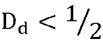
- the transistor controller is configured to turn off the first transistor, turn on the second transistor and the third transistor, and control a first coefficient, so that in response to that the first coefficient is less than 1/2, a voltage between the second positive end and the second negative end of the boost and buck apparatus is less than a voltage of the power battery, and in response to that the first coefficient is greater than 1/2, the voltage between the second positive end and the second negative end of the boost and buck apparatus is greater than the voltage of the power battery; and the first coefficient is a ratio of a turn-on time of the second transistor and the third transistor to a sum of the turn-on time of the second transistor and the third transistor and a turn-off time of the second transistor and the third transistor.
- the transistor controller in response to that the vehicle is in the charging mode, is connected to a positive electrode of the charging station and the second negative end of the boost and buck apparatus is connected to a negative electrode of the charging station, the transistor controller is configured to turn off the second transistor, turn on the first transistor and the third transistor in turn, and control a second coefficient, so that in response to that the second coefficient is greater than zero, a voltage between the first positive end and the first negative end of the boost and buck apparatus is greater than a voltage of the charging station; and the second coefficient is a ratio of a turn-on-time of the first transistor to a sum of the turn-on-time of the first transistor and a turn-off-time of the first transistor.
- Embodiments of the present application provides a boost and buck system, applied to a new energy vehicle, including a boost and buck apparatus, a switch, an inverter, a charging station, a power battery and a switch controller; the boost and buck apparatus includes a boost and buck circuit and a transistor controller;
- the boost and buck circuit is further configured to output a second output voltage under second control of the transistor controller, the second output voltage is greater than a second input voltage, the second input voltage is a voltage of an external charging station, and the second output voltage is configured to charge the external power battery; and the transistor controller is further configured to output the second control to the boost and buck circuit in response to that the vehicle is in a charging mode, and the second control is the second on/off control of the controllable device of the boost and buck circuit.
- the boost and buck circuit includes a first capacitance, an inductance, a diode, a first transistor, a second transistor, a third transistor, and a second capacitance;
- the transistor controller is configured to turn off the first transistor, turn on the second transistor and the third transistor, and control a first coefficient, so that in response to that the first coefficient is less than 1/2, a voltage between the second positive end and the second negative end of the boost and buck apparatus is less than a voltage of the power battery, and in response to that the first coefficient is greater than 1/2, the voltage between the second positive end and the second negative end of the boost and buck apparatus is greater than the voltage of the power battery; and the first coefficient is a ratio of a turn-on time of the second transistor and the third transistor to a sum of the turn-on time of the second transistor and the third transistor and a turn-off time of the second transistor and the third transistor.
- the transistor controller in response to that the vehicle is in the charging mode, is connected to a positive electrode of the charging station and the second negative end of the boost and buck apparatus is connected to a negative electrode of the charging station, the transistor controller is configured to turn off the second transistor, turn on the first transistor and the third transistor in turn, and control a second coefficient, so that in response to that the second coefficient is greater than zero, a voltage between the first positive end and the first negative end of the boost and buck apparatus is greater than a voltage of the charging station; and the second coefficient is a ratio of a turn-on-time of the first transistor to a sum of the turn-on-time of the first transistor and a turn-off-time of the first transistor.
- the switch includes a first switch and a second switch, and each switch includes a fixed end, a first moving end, and a second moving end;
- the switch controller is configured to connect the fixed end of the first switch to the second moving end of the first switch and connect the fixed end of the second switch to the second moving end of the second switch in response to that the vehicle is in the drive mode, and configured to connect the fixed end of the first switch to the first moving end of the first switch and connect the fixed end of the second switch to the first moving end of the second switch in response to the vehicle is in the charging mode.
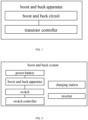
- FIG. 1 is a schematic diagram of a boost and buck apparatus according to an embodiment of the present application. As shown in FIG. 1 , the boost and buck apparatus of this embodiment is applied to a new energy vehicle.
- the boost and buck apparatus includes a boost and buck circuit and a transistor controller.
- the boost and buck circuit is configured to output a first output voltage under the first control of the transistor controller, and the first output voltage is greater than or less than the first input voltage.
- the first input voltage is the voltage of an external power battery, and the first output voltage is configured to supply power to the inverter of the vehicle motor.
- the transistor controller is configured to output first control to the boost and buck circuit in response to that the vehicle is in a drive mode.
- the first control refers to the first on/off control of the controllable device of the boost and buck circuit.
- the boost and buck circuit is further configured to output a second output voltage under the second control of the transistor controller, and the second output voltage is greater than the second input voltage.
- the second input voltage is the voltage of the external charging station, and the second output voltage is configured to charge the external power battery.
- the transistor controller is further configured to output second control to the boost and buck circuit in response to that the vehicle is in the charging mode.
- the second control refers to the second on/off control of the controllable device of the boost and buck circuit.
- the boost and buck circuit includes a first capacitance, an inductance, a diode, a first transistor, a second transistor, a third transistor, and a second capacitance.
- the first end of the first capacitance serves as the first negative end of the boost and buck apparatus
- the second end of the first capacitance serves as the first positive end of the boost and buck apparatus
- the first end of the second capacitance serves as the second positive end of the boost and buck apparatus
- the second end of the second capacitance serves as the second negative end of the boost and buck apparatus.
- the first end of the first capacitance is respectively connected to the anode of the diode and the first end of the second transistor, the second end of the second transistor is respectively connected to the first end of the inductance and the first end of the second capacitance, the second end of the first capacitance is connected to the first end of the third transistor, the second end of the third transistor is respectively connected to the first end of the first transistor and the second end of the inductance, and the second end of the first transistor is respectively connected to the cathode of the diode and the second end of the second capacitance.
- the transistor controller in response to that the vehicle is in the drive mode, that is, the first positive end of the boost and buck apparatus is connected to the positive electrode of the power battery and the first negative end of the boost and buck apparatus is connected to the negative electrode of the power battery, the transistor controller is configured to turn off the first transistor, and turn on the second transistor and the third transistor, and control the first coefficient In this way, in response to that the first coefficient is less than 1/2, the voltage between the second positive end and the second negative end of the boost and buck apparatus is less than the voltage of the power battery; in response to that the first coefficient is greater than 1/2, the voltage between the second positive end and the second negative end of the boost and buck apparatus is greater than the voltage of the power battery.
- the first coefficient refers to the ratio of the turn-on-time of the second transistor and the third transistor to the sum of the turn-on-time of the second transistor and the third transistor and the turn-off-time of the second transistor and the third transistor.
- the first control may refer to turning off the first transistor, turning on the second transistor and the third transistor, and controlling the first coefficient.
- Controlling the first coefficient may refer to controlling the turn-on-time of the second transistor and the third transistor.
- the first transistor, the second transistor, and the third transistor may be silicon carbide thyristors.
- the first end of the transistor may be the anode of the silicon carbide thyristor
- the second end may be the cathode of the silicon carbide thyristor
- the gate electrode of the silicon carbide thyristor serves as the control electrode.
- the first transistor, the second transistor, and the third transistor may be silicon carbide triodes.
- the first end of the transistor may be the source electrode/drain electrode of the silicon carbide triode
- the second end may be the drain electrode/source electrode of the silicon carbide triode
- the gate electrode of the silicon carbide triode serves as the control electrode.
- the third transistor and the second transistor are turned on at the same time and turned off at the same time.
- the transistor controller in response to that the vehicle is in the charging mode, that is, the second positive end of the boost and buck apparatus is connected to the positive electrode of the charging station and the second negative end of the boost and buck apparatus is connected to the negative electrode of the charging station, the transistor controller is configured to turn off the second transistor, and turn on the first transistor and the third transistor in turn, and control the second coefficient. In this way, in response to that the second coefficient is greater than zero, the voltage between the first positive end and the first negative end of the boost and buck apparatus is greater than the voltage of the charging station.
- the second coefficient refers to the ratio of the turn-on-time of the first transistor to the sum of the turn-on-time of the first transistor and the turn-off-time of the first transistor.
- the second control may refer to turning off the second transistor, turning on the first transistor and the third transistor in turn, and controlling the second coefficient.
- Controlling the second coefficient may refer to controlling the turn-on-time of the first transistor.
- the boost and buck apparatus in the present application can realize both the boost discharge function and the buck discharge function in the same apparatus.
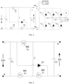
- FIG. 2 is a schematic diagram of a boost and buck system according to an embodiment of the present application.
- the boost and buck system includes a boost and buck apparatus, a switch, an inverter, a charging station, a power battery and a switch controller.
- the boost and buck apparatus includes a boost and buck circuit and the transistor controller.
- the boost and buck circuit is configured to output a first output voltage under the first control of the transistor controller, and the first output voltage is greater than or less than the first input voltage.
- the first input voltage is the voltage of the power battery, and the first output voltage is configured to supply power to the inverter of the vehicle motor.
- the transistor controller is configured to output first control to the boost and buck circuit in response to that the vehicle is in the drive mode.
- the first control refers to the first on/off control of the controllable device of the boost and buck circuit.
- the switch controller is configured to shift the switch to the inverter side in response to that the vehicle is in the drive mode, so that the boost and buck apparatus is connected to the inverter. In response to that the vehicle is in the charging mode, the switch is shifted to the charging station side, so that the boost and buck apparatus is connected to the charging station.
- the boost and buck circuit is further configured to output a second output voltage under the second control of the transistor controller, and the second output voltage is greater than the second input voltage.
- the second input voltage is the voltage of the charging station, and the second output voltage is configured to charge the power battery.
- the transistor controller is further configured to output second control to the boost and buck circuit in response to that the vehicle is in the charging mode.
- the second control refers to the second on/off control of the controllable device of the boost and buck circuit.
- the boost and buck circuit includes a first capacitance, an inductance, a diode, a first transistor, a second transistor, a third transistor, and a second capacitance.
- the first end of the first capacitance serves as the first negative end of the boost and buck apparatus
- the second end of the first capacitance serves as the first positive end of the boost and buck apparatus
- the first end of the second capacitance serves as the second positive end of the boost and buck apparatus
- the second end of the second capacitance serves as the second negative end of the boost and buck apparatus.
- the first end of the first capacitance is respectively connected to the anode of the diode and the first end of the second transistor, the second end of the second transistor is respectively connected to the first end of the inductance and the first end of the second capacitance, the second end of the first capacitance is connected to the first end of the third transistor, the second end of the third transistor is respectively connected to the first end of the first transistor and the second end of the inductance, and the second end of the first transistor is respectively connected to the cathode of the diode and the second end of the second capacitance.
- the first transistor, the second transistor, and the third transistor may be silicon carbide thyristors.
- the first end of the transistor can be the anode of the silicon carbide thyristor
- the second end can be the cathode of the silicon carbide thyristor
- the gate electrode of the silicon carbide thyristor serves as the control electrode.
- the first transistor, the second transistor, and the third transistor can be silicon carbide triodes.
- the first end of the transistor can be the source electrode/drain electrode of the silicon carbide triode
- the second end can be the drain electrode/source electrode of the silicon carbide triode
- the gate electrode of the silicon carbide triode serves as the control electrode.
- the transistor controller in response to that the vehicle is in the drive mode, that is, the first positive end of the boost and buck apparatus is connected to the positive electrode of the power battery and the first negative end of the boost and buck apparatus is connected to the negative electrode of the power battery, the transistor controller is configured to turn off the first transistor, turn on the second transistor and the third transistor, and control the first coefficient.
- the first coefficient is less than 1/2
- the voltage between the second positive end and the second negative end of the boost and buck apparatus is less than the voltage of the power battery
- the first coefficient in response to that the first coefficient is greater than 1/2, the voltage between the second positive end and the second negative end of the boost and buck apparatus is greater than the voltage of the power battery.
- the first coefficient refers to the ratio of the turn-on-time of the second transistor and the third transistor to the sum of the turn-on-time of the second transistor and the third transistor, and the turn-off-time of the second transistor and the third transistor.
- the first control may refer to turning off the first transistor, turning on the second transistor and the third transistor, and controlling the first coefficient.
- Controlling the first coefficient may refer to controlling the turn-on-time of the second transistor and the third transistor.
- the transistor controller in response to that the vehicle is in the charging mode, that is, the second positive end of the boost and buck apparatus is connected to the positive electrode of the charging station and the second negative end of the boost and buck apparatus is connected to the negative electrode of the charging station, the transistor controller is specifically configured to turn off the second transistor, turn on the first transistor and the third transistor in turn, and control the second coefficient. In this way, in response to that the second coefficient is greater than zero, the voltage between the first positive end and the first negative end of the boost and buck apparatus is greater than the voltage of the charging station.
- the second coefficient refers to the ratio of the turn-on-time of the first transistor to the sum of the turn-on-time of the first transistor and the turn-off-time of the first transistor.
- the second control may refer to turning off the second transistor, turning on the first transistor and the third transistor in turn, and controlling the second coefficient.
- Controlling the second coefficient may refer to controlling the turn-on-time of the first transistor.
- two switches including a first switch and a second switch are provided, and each of the switches includes a fixed end, a first moving end, and a second moving end.
- the fixed end of the first switch is connected to the second positive end of the boost and buck apparatus, the first moving end of the first switch is connected to the positive electrode of the charging station, and the second moving end of the first switch is connected to the positive electrode input end of the inverter.
- the fixed end of the second switch is connected to the second negative end of the boost and buck apparatus, the first moving end of the second switch is connected to the negative electrode of the charging station, and the second moving end of the second switch is connected to the negative electrode input end of the inverter.
- the switch controller is configured to connect the fixed end of the first switch to the second moving end of the first switch and the fixed end of the second switch to the second moving end of the second switch in response to that the vehicle is in the drive mode; and configured to connect the fixed end of the first switch to the first moving end of the first switch and the fixed end of the second switch to the first moving end of the second switch in response to that the vehicle is in the charging mode.
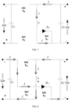
- FIG. 3 is a schematic diagram of another boost and buck system according to an embodiment of the present application.
- U in is the input voltage (i.e., the output voltage of the power battery) in the drive mode
- U o is the output voltage
- D 1 is the diode
- S 1 , S 2 , and S 3 are the silicon carbide (SiC) thyristors (SiC can be bidirectionally conductive)
- L is the inductance
- C 1 and C 2 are the vehicle film capacitance
- S a1 and S a2 are the two thyristor IGBT groups on the corresponding half bridge of the three-phase motor A.
- S b1 and S b2 corresponds to the B phase
- S c1 corresponds to the C phase
- the stator winding of the three-phase motor M is a star connection, where point N is the neutral point of the three-phase winding.
- the switches SW1 and SW2 are set to the upper position, the whole vehicle is in the charging mode and is connected to the charging station, and the charging station charges the power battery; in response to that the switches SW1 and SW2 are set to the lower position, the whole vehicle is in the drive mode and is connected to the inverter of the motor, and the input voltage is input to the motor.
- the boost and buck circuit shown in FIG. 4 includes a capacitance C1, a capacitance C2, a thyristor S1, a thyristor S2, a thyristor S3, a diode D1, and an inductance L.
- the voltage of capacitance C2 is U 0 .
- the BOOST/BUCK function is described as follows: At this time, the voltage U o is output by the power battery U in after being boosted and reduced, and the control method of S 1 , S 2 and S 3 is as follows:
- the control method is described as follows: the switching frequencies of the three silicon carbide thyristors S 1 , S 2 and S 3 are the same, that is, the switching cycles T d are the same (d represents Driving).
- the control duty cycle of S 2 and S 3 is D d
- the duty cycle of S 1 is (1-D d ). That is, in response to that S 3 and S 2 are turned on, S 1 is turned off; and in response to that S 3 and S 2 are turned off, S 1 is turned on, which are complementary.
- the Boost function is described as follows: In this mode, U o charges the battery pack U in as the energy input end, S 2 is in a normal turn-off state.
- the control method of S 1 and S 3 is as follows:
- S 2 is in a normal turn-off state in this mode, the switching frequencies of S 1 and S 3 are the same, that is, the switching cycles T g are the same (g represents Generating).
- the duty cycle of S 1 is D g and the duty cycle of S 3 is (1-D g ). That is, in response to that S 1 is turned on, S 3 is turned off; and in response to that S 1 is turned off, and S 3 is turned on, which are complementary.
- the bus voltage input to the inverter can be boosted and bucked by controlling the conduction duty cycle of the specific SiC in the buck-boost apparatus, and the target value of the buck-boost is calculated according to the first formula.
- the voltage input to the power battery can be boosted and charged by controlling the conduction duty cycle of the specific SiC in the buck-boost apparatus, and the target value of the boost is calculated according to the second formula.
- the term computer storage media includes volatile and non-volatile, removable and non-removable media implemented in any method or technology that is configured to store information (such as computer-readable instructions, data structures, program modules, or other data).
- the computer storage media include, but are not limited to, RAM, ROM, EEPROM, flash memory or other memory technology, CD-ROM, digital versatile disk (DVD) or other optical disk storage, magnetic cassettes, magnetic tapes, magnetic disk storage or other magnetic storage apparatus, or any other medium that can be configured to store the desired information and can be accessed by a computer.
- the communication media typically contain computer-readable instructions, data structures, program modules, or other data in a modulated data signal such as a carrier wave or other transport mechanism, and may include any information delivery media.
Landscapes
- Engineering & Computer Science (AREA)
- Power Engineering (AREA)
- Transportation (AREA)
- Mechanical Engineering (AREA)
- Life Sciences & Earth Sciences (AREA)
- Sustainable Development (AREA)
- Sustainable Energy (AREA)
- Dc-Dc Converters (AREA)
- Inverter Devices (AREA)
- Charge And Discharge Circuits For Batteries Or The Like (AREA)
- Electric Propulsion And Braking For Vehicles (AREA)
Abstract
Embodiments of the present application provides a boost and buck apparatus and a boost and buck system. The boost and buck apparatus includes: a boost and buck circuit configured to output a first output voltage under first control of a transistor controller, the first output voltage being greater than or less than a first input voltage, the first input voltage being a voltage of an external power battery, and the first output voltage being configured to supply power to an inverter of a vehicle motor; and a transistor controller configured to output the first control to the boost and buck circuit in response to that the vehicle is in a drive mode, and the first control being first on/off control of a controllable device of the boost and buck circuit.
Description
- The present application claims priority to
Chinese Patent Application No. 202310026367.X, filed on January 9, 2023 - The embodiments of the present application relate to, but are not limited to, the technical field of power electronics, and in particular to a boost and buck apparatus and a boost and buck system.
- There are some apparatuses in power electronic equipment that achieve specific functions by increasing or decreasing the input voltage, which are usually called as boost apparatuses or buck apparatuses, and are represented in new energy vehicles as BOOST and BUCK. However, currently only the boost discharge function or the buck discharge function can be realized in the same apparatus.
- The following is an overview of the subject matter described in detail herein, which is not intended to limit the scope of the claims.
- Embodiments of the present application provides a boost and buck apparatus, applied to a new energy vehicle, including a boost and buck circuit and a transistor controller;
- the boost and buck circuit is configured to output a first output voltage under first control of the transistor controller, the first output voltage is greater than or less than a first input voltage, the first input voltage is a voltage of an external power battery, and the first output voltage is configured to supply power to an inverter of a vehicle motor; and
- the transistor controller is configured to output the first control to the boost and buck circuit in response to that the vehicle is in a drive mode, and the first control is the first on/off control of a controllable device of the boost and buck circuit.
- In an embodiment, the boost and buck circuit is further configured to output a second output voltage under second control of the transistor controller, the second output voltage is greater than a second input voltage, the second input voltage is a voltage of an external charging station, and the second output voltage is configured to charge the external power battery; and
the transistor controller is further configured to output the second control to the boost and buck circuit in response to that the vehicle is in a charging mode, and the second control is the second on/off control of the controllable device of the boost and buck circuit. - In an embodiment, the boost and buck circuit includes a first capacitance, an inductance, a diode, a first transistor, a second transistor, a third transistor, and a second capacitance;
- a first end of the first capacitance serves as a first negative end of the boost and buck apparatus, a second end of the first capacitance serves as a first positive end of the boost and buck apparatus, a first end of the second capacitance serves as a second positive end of the boost and buck apparatus, and a second end of the second capacitance serves as a second negative end of the boost and buck apparatus; and
- the first end of the first capacitance is respectively connected to an anode of the diode and a first end of the second transistor, a second end of the second transistor is respectively connected to a first end of the inductance and the first end of the second capacitance, the second end of the first capacitance is connected to a first end of the third transistor, a second end of the third transistor is respectively connected to a first end of the first transistor and a second end of the inductance, and a second end of the first transistor is respectively connected to a cathode of the diode and the second end of the second capacitance.
- In an embodiment, in response to that the vehicle is in the drive mode, the first positive end of the boost and buck apparatus is connected to a positive electrode of the power battery and the first negative end of the boost and buck apparatus is connected to a negative electrode of the power battery, the transistor controller is configured to turn off the first transistor, turn on the second transistor and the third transistor, and control a first coefficient, so that in response to that the first coefficient is less than 1/2, a voltage between the second positive end and the second negative end of the boost and buck apparatus is less than a voltage of the power battery, and in response to that the first coefficient is greater than 1/2, the voltage between the second positive end and the second negative end of the boost and buck apparatus is greater than the voltage of the power battery; and
the first coefficient is a ratio of a turn-on time of the second transistor and the third transistor to a sum of the turn-on time of the second transistor and the third transistor and a turn-off time of the second transistor and the third transistor. - In an embodiment, in response to that the vehicle is in the charging mode, the second positive end of the boost and buck apparatus is connected to a positive electrode of the charging station and the second negative end of the boost and buck apparatus is connected to a negative electrode of the charging station, the transistor controller is configured to turn off the second transistor, turn on the first transistor and the third transistor in turn, and control a second coefficient, so that in response to that the second coefficient is greater than zero, a voltage between the first positive end and the first negative end of the boost and buck apparatus is greater than a voltage of the charging station; and
the second coefficient is a ratio of a turn-on-time of the first transistor to a sum of the turn-on-time of the first transistor and a turn-off-time of the first transistor. - Embodiments of the present application provides a boost and buck system, applied to a new energy vehicle, including a boost and buck apparatus, a switch, an inverter, a charging station, a power battery and a switch controller; the boost and buck apparatus includes a boost and buck circuit and a transistor controller;
- the boost and buck circuit is configured to output a first output voltage under first control of the transistor controller, the first output voltage is greater than or less than a first input voltage, the first input voltage is a voltage of an external power battery, and the first output voltage is configured to supply power to an inverter of a vehicle motor; and
- the transistor controller is configured to output the first control to the boost and buck circuit in response to that the vehicle is in a drive mode, and the first control is the first on/off control of a controllable device of the boost and buck circuit;
- the switch controller is configured to shift the switch to an inverter side in response to that the vehicle is in the drive mode, so that the boost and buck apparatus is connected to the inverter; and
- the switch controller is configured to shift the switch to a charging station side in response to that the vehicle is in the charging mode, so that the boost and buck apparatus is connected to the charging station.
- In an embodiment, the boost and buck circuit is further configured to output a second output voltage under second control of the transistor controller, the second output voltage is greater than a second input voltage, the second input voltage is a voltage of an external charging station, and the second output voltage is configured to charge the external power battery; and
the transistor controller is further configured to output the second control to the boost and buck circuit in response to that the vehicle is in a charging mode, and the second control is the second on/off control of the controllable device of the boost and buck circuit. - In an embodiment, the boost and buck circuit includes a first capacitance, an inductance, a diode, a first transistor, a second transistor, a third transistor, and a second capacitance;
- a first end of the first capacitance serves as a first negative end of the boost and buck apparatus, a second end of the first capacitance serves as a first positive end of the boost and buck apparatus, a first end of the second capacitance serves as a second positive end of the boost and buck apparatus, and a second end of the second capacitance serves as a second negative end of the boost and buck apparatus; and
- the first end of the first capacitance is respectively connected to an anode of the diode and a first end of the second transistor, a second end of the second transistor is respectively connected to a first end of the inductance and the first end of the second capacitance, the second end of the first capacitance is connected to a first end of the third transistor, a second end of the third transistor is respectively connected to a first end of the first transistor and a second end of the inductance, and a second end of the first transistor is respectively connected to a cathode of the diode and the second end of the second capacitance.
- In an embodiment, in response to that the vehicle is in the drive mode, the first positive end of the boost and buck apparatus is connected to a positive electrode of the power battery and the first negative end of the boost and buck apparatus is connected to a negative electrode of the power battery, the transistor controller is configured to turn off the first transistor, turn on the second transistor and the third transistor, and control a first coefficient, so that in response to that the first coefficient is less than 1/2, a voltage between the second positive end and the second negative end of the boost and buck apparatus is less than a voltage of the power battery, and in response to that the first coefficient is greater than 1/2, the voltage between the second positive end and the second negative end of the boost and buck apparatus is greater than the voltage of the power battery; and
the first coefficient is a ratio of a turn-on time of the second transistor and the third transistor to a sum of the turn-on time of the second transistor and the third transistor and a turn-off time of the second transistor and the third transistor. - In an embodiment, in response to that the vehicle is in the charging mode, the second positive end of the boost and buck apparatus is connected to a positive electrode of the charging station and the second negative end of the boost and buck apparatus is connected to a negative electrode of the charging station, the transistor controller is configured to turn off the second transistor, turn on the first transistor and the third transistor in turn, and control a second coefficient, so that in response to that the second coefficient is greater than zero, a voltage between the first positive end and the first negative end of the boost and buck apparatus is greater than a voltage of the charging station; and
the second coefficient is a ratio of a turn-on-time of the first transistor to a sum of the turn-on-time of the first transistor and a turn-off-time of the first transistor. - In an embodiment, the switch includes a first switch and a second switch, and each switch includes a fixed end, a first moving end, and a second moving end;
- a fixed end of the first switch is connected to the second positive end of the boost and buck apparatus, a first moving end of the first switch is connected to the positive electrode of the charging station, and a second moving end of the first switch is connected to an input end of a positive electrode of the inverter; and
- a fixed end of the second switch is connected to the second negative end of the boost and buck apparatus, a first moving end of the second switch is connected to the negative electrode of the charging station, and a second moving end of the second switch is connected to an input end of a negative electrode of the inverter.
- In an embodiment, the switch controller is configured to connect the fixed end of the first switch to the second moving end of the first switch and connect the fixed end of the second switch to the second moving end of the second switch in response to that the vehicle is in the drive mode, and configured to connect the fixed end of the first switch to the first moving end of the first switch and connect the fixed end of the second switch to the first moving end of the second switch in response to the vehicle is in the charging mode.
- Other aspects can be understood after reading and understanding the accompanying drawings and detailed descriptions.
- The accompanying drawings are used to provide an understanding of the technical solution of the present application and constitute a part of the specification. Together with the embodiments of the present application, they are used to explain the technical solution of the present application and do not constitute a limitation on the technical solution of the present application.
-
FIG. 1 is a schematic diagram of a boost and buck apparatus according to an embodiment of the present application. -
FIG. 2 is a schematic diagram of a boost and buck system according to an embodiment of the present application. -
FIG. 3 is a schematic diagram of another boost and buck system according to an embodiment of the present application. -
FIG. 4 is a schematic structural diagram of the buck-boost apparatus in the system shown inFIG. 3 . -
FIG. 5 is a schematic circuit diagram where S2 and S3 are turned on and S1 is turned off in the system shown inFIG. 3 . -
FIG. 6 is a schematic circuit diagram where S3 and S2 are turned off and S1 is turned on in the system shown inFIG. 3 . -
FIG. 7 is a schematic circuit diagram where S3 and S2 are turned off and S1 is turned on in the system shown inFIG. 3 . -
FIG. 8 is a schematic circuit diagram where S1 is turned off and S3 and S2 are turned on in the system shown inFIG. 3 . -
FIG. 1 is a schematic diagram of a boost and buck apparatus according to an embodiment of the present application. As shown inFIG. 1 , the boost and buck apparatus of this embodiment is applied to a new energy vehicle. The boost and buck apparatus includes a boost and buck circuit and a transistor controller. - The boost and buck circuit is configured to output a first output voltage under the first control of the transistor controller, and the first output voltage is greater than or less than the first input voltage. The first input voltage is the voltage of an external power battery, and the first output voltage is configured to supply power to the inverter of the vehicle motor.
- The transistor controller is configured to output first control to the boost and buck circuit in response to that the vehicle is in a drive mode. The first control refers to the first on/off control of the controllable device of the boost and buck circuit.
- In an embodiment, the boost and buck circuit is further configured to output a second output voltage under the second control of the transistor controller, and the second output voltage is greater than the second input voltage. The second input voltage is the voltage of the external charging station, and the second output voltage is configured to charge the external power battery.
- The transistor controller is further configured to output second control to the boost and buck circuit in response to that the vehicle is in the charging mode. The second control refers to the second on/off control of the controllable device of the boost and buck circuit.
- In an embodiment, the boost and buck circuit includes a first capacitance, an inductance, a diode, a first transistor, a second transistor, a third transistor, and a second capacitance.
- The first end of the first capacitance serves as the first negative end of the boost and buck apparatus, the second end of the first capacitance serves as the first positive end of the boost and buck apparatus, the first end of the second capacitance serves as the second positive end of the boost and buck apparatus, and the second end of the second capacitance serves as the second negative end of the boost and buck apparatus.
- The first end of the first capacitance is respectively connected to the anode of the diode and the first end of the second transistor, the second end of the second transistor is respectively connected to the first end of the inductance and the first end of the second capacitance, the second end of the first capacitance is connected to the first end of the third transistor, the second end of the third transistor is respectively connected to the first end of the first transistor and the second end of the inductance, and the second end of the first transistor is respectively connected to the cathode of the diode and the second end of the second capacitance.
- In an embodiment, in response to that the vehicle is in the drive mode, that is, the first positive end of the boost and buck apparatus is connected to the positive electrode of the power battery and the first negative end of the boost and buck apparatus is connected to the negative electrode of the power battery, the transistor controller is configured to turn off the first transistor, and turn on the second transistor and the third transistor, and control the first coefficient In this way, in response to that the first coefficient is less than 1/2, the voltage between the second positive end and the second negative end of the boost and buck apparatus is less than the voltage of the power battery; in response to that the first coefficient is greater than 1/2, the voltage between the second positive end and the second negative end of the boost and buck apparatus is greater than the voltage of the power battery.
- The first coefficient refers to the ratio of the turn-on-time of the second transistor and the third transistor to the sum of the turn-on-time of the second transistor and the third transistor and the turn-off-time of the second transistor and the third transistor.
- The first control may refer to turning off the first transistor, turning on the second transistor and the third transistor, and controlling the first coefficient. Controlling the first coefficient may refer to controlling the turn-on-time of the second transistor and the third transistor.
- In an embodiment, the first transistor, the second transistor, and the third transistor may be silicon carbide thyristors. At this time, the first end of the transistor may be the anode of the silicon carbide thyristor, the second end may be the cathode of the silicon carbide thyristor, and the gate electrode of the silicon carbide thyristor serves as the control electrode.
- In an embodiment, the first transistor, the second transistor, and the third transistor may be silicon carbide triodes. At this time, the first end of the transistor may be the source electrode/drain electrode of the silicon carbide triode, the second end may be the drain electrode/source electrode of the silicon carbide triode, and the gate electrode of the silicon carbide triode serves as the control electrode.
- For example, the first coefficient is


- In an embodiment, in response to that the vehicle is in the charging mode, that is, the second positive end of the boost and buck apparatus is connected to the positive electrode of the charging station and the second negative end of the boost and buck apparatus is connected to the negative electrode of the charging station, the transistor controller is configured to turn off the second transistor, and turn on the first transistor and the third transistor in turn, and control the second coefficient. In this way, in response to that the second coefficient is greater than zero, the voltage between the first positive end and the first negative end of the boost and buck apparatus is greater than the voltage of the charging station.
- The second coefficient refers to the ratio of the turn-on-time of the first transistor to the sum of the turn-on-time of the first transistor and the turn-off-time of the first transistor.
- The second control may refer to turning off the second transistor, turning on the first transistor and the third transistor in turn, and controlling the second coefficient. Controlling the second coefficient may refer to controlling the turn-on-time of the first transistor. For example, the second coefficient is


- The boost and buck apparatus in the present application can realize both the boost discharge function and the buck discharge function in the same apparatus.
-
FIG. 2 is a schematic diagram of a boost and buck system according to an embodiment of the present application. As shown inFIG. 2 , the boost and buck system includes a boost and buck apparatus, a switch, an inverter, a charging station, a power battery and a switch controller. The boost and buck apparatus includes a boost and buck circuit and the transistor controller. - The boost and buck circuit is configured to output a first output voltage under the first control of the transistor controller, and the first output voltage is greater than or less than the first input voltage. The first input voltage is the voltage of the power battery, and the first output voltage is configured to supply power to the inverter of the vehicle motor.
- The transistor controller is configured to output first control to the boost and buck circuit in response to that the vehicle is in the drive mode. The first control refers to the first on/off control of the controllable device of the boost and buck circuit.
- The switch controller is configured to shift the switch to the inverter side in response to that the vehicle is in the drive mode, so that the boost and buck apparatus is connected to the inverter. In response to that the vehicle is in the charging mode, the switch is shifted to the charging station side, so that the boost and buck apparatus is connected to the charging station.
- In an embodiment, the boost and buck circuit is further configured to output a second output voltage under the second control of the transistor controller, and the second output voltage is greater than the second input voltage. The second input voltage is the voltage of the charging station, and the second output voltage is configured to charge the power battery.
- The transistor controller is further configured to output second control to the boost and buck circuit in response to that the vehicle is in the charging mode. The second control refers to the second on/off control of the controllable device of the boost and buck circuit.
- In an embodiment, the boost and buck circuit includes a first capacitance, an inductance, a diode, a first transistor, a second transistor, a third transistor, and a second capacitance.
- The first end of the first capacitance serves as the first negative end of the boost and buck apparatus, the second end of the first capacitance serves as the first positive end of the boost and buck apparatus, the first end of the second capacitance serves as the second positive end of the boost and buck apparatus;, and the second end of the second capacitance serves as the second negative end of the boost and buck apparatus.
- The first end of the first capacitance is respectively connected to the anode of the diode and the first end of the second transistor, the second end of the second transistor is respectively connected to the first end of the inductance and the first end of the second capacitance, the second end of the first capacitance is connected to the first end of the third transistor, the second end of the third transistor is respectively connected to the first end of the first transistor and the second end of the inductance, and the second end of the first transistor is respectively connected to the cathode of the diode and the second end of the second capacitance.
- In an embodiment, the first transistor, the second transistor, and the third transistor may be silicon carbide thyristors. At this time, the first end of the transistor can be the anode of the silicon carbide thyristor, the second end can be the cathode of the silicon carbide thyristor, and the gate electrode of the silicon carbide thyristor serves as the control electrode.
- In an embodiment, the first transistor, the second transistor, and the third transistor can be silicon carbide triodes. At this time, the first end of the transistor can be the source electrode/drain electrode of the silicon carbide triode, the second end can be the drain electrode/source electrode of the silicon carbide triode, and the gate electrode of the silicon carbide triode serves as the control electrode.
- In an embodiment, in response to that the vehicle is in the drive mode, that is, the first positive end of the boost and buck apparatus is connected to the positive electrode of the power battery and the first negative end of the boost and buck apparatus is connected to the negative electrode of the power battery, the transistor controller is configured to turn off the first transistor, turn on the second transistor and the third transistor, and control the first coefficient. In this way, in response to that the first coefficient is less than 1/2, the voltage between the second positive end and the second negative end of the boost and buck apparatus is less than the voltage of the power battery; in response to that the first coefficient is greater than 1/2, the voltage between the second positive end and the second negative end of the boost and buck apparatus is greater than the voltage of the power battery.
- The first coefficient refers to the ratio of the turn-on-time of the second transistor and the third transistor to the sum of the turn-on-time of the second transistor and the third transistor, and the turn-off-time of the second transistor and the third transistor.
- The first control may refer to turning off the first transistor, turning on the second transistor and the third transistor, and controlling the first coefficient. Controlling the first coefficient may refer to controlling the turn-on-time of the second transistor and the third transistor.
- In an embodiment, in response to that the vehicle is in the charging mode, that is, the second positive end of the boost and buck apparatus is connected to the positive electrode of the charging station and the second negative end of the boost and buck apparatus is connected to the negative electrode of the charging station, the transistor controller is specifically configured to turn off the second transistor, turn on the first transistor and the third transistor in turn, and control the second coefficient. In this way, in response to that the second coefficient is greater than zero, the voltage between the first positive end and the first negative end of the boost and buck apparatus is greater than the voltage of the charging station.
- The second coefficient refers to the ratio of the turn-on-time of the first transistor to the sum of the turn-on-time of the first transistor and the turn-off-time of the first transistor.
- The second control may refer to turning off the second transistor, turning on the first transistor and the third transistor in turn, and controlling the second coefficient. Controlling the second coefficient may refer to controlling the turn-on-time of the first transistor.
- In an embodiment, two switches, including a first switch and a second switch are provided, and each of the switches includes a fixed end, a first moving end, and a second moving end.
- The fixed end of the first switch is connected to the second positive end of the boost and buck apparatus, the first moving end of the first switch is connected to the positive electrode of the charging station, and the second moving end of the first switch is connected to the positive electrode input end of the inverter.
- The fixed end of the second switch is connected to the second negative end of the boost and buck apparatus, the first moving end of the second switch is connected to the negative electrode of the charging station, and the second moving end of the second switch is connected to the negative electrode input end of the inverter.
- In an embodiment, the switch controller is configured to connect the fixed end of the first switch to the second moving end of the first switch and the fixed end of the second switch to the second moving end of the second switch in response to that the vehicle is in the drive mode; and configured to connect the fixed end of the first switch to the first moving end of the first switch and the fixed end of the second switch to the first moving end of the second switch in response to that the vehicle is in the charging mode.
-
FIG. 3 is a schematic diagram of another boost and buck system according to an embodiment of the present application. As shown inFIG. 3 , Uin is the input voltage (i.e., the output voltage of the power battery) in the drive mode, Uo is the output voltage, D1 is the diode, S1, S2, and S3 are the silicon carbide (SiC) thyristors (SiC can be bidirectionally conductive), L is the inductance, C1 and C2 are the vehicle film capacitance, and Sa1 and Sa2 are the two thyristor IGBT groups on the corresponding half bridge of the three-phase motor A. Similarly, Sb1 and Sb2 corresponds to the B phase, and Sc1, and corresponds to the C phase. The stator winding of the three-phase motor M is a star connection, where point N is the neutral point of the three-phase winding. In response to that the switches SW1 and SW2 are set to the upper position, the whole vehicle is in the charging mode and is connected to the charging station, and the charging station charges the power battery; in response to that the switches SW1 and SW2 are set to the lower position, the whole vehicle is in the drive mode and is connected to the inverter of the motor, and the input voltage is input to the motor. - The boost and buck circuit shown in
FIG. 4 includes a capacitance C1, a capacitance C2, a thyristor S1, a thyristor S2, a thyristor S3, a diode D1, and an inductance L. The voltage of capacitance C2 is U 0. - In the drive mode, the BOOST/BUCK function is described as follows:
At this time, the voltage Uo is output by the power battery Uin after being boosted and reduced, and the control method of S1, S2 and S3 is as follows: - in response to that S2 and S3 are turned on and S1 is turned off, the inductance L stores energy, as shown in
FIG. 5 below, and the flow direction of the current I is marked in the figure; - in response to that S2 and S3 are turned off and S1 is turned on, the inductance L releases energy, and the circuit is shown in
FIG. 6 . - The control method is described as follows:
the switching frequencies of the three silicon carbide thyristors S1, S2 and S3 are the same, that is, the switching cycles Td are the same (d represents Driving). The control duty cycle of S2 and S3 is Dd, and the duty cycle of S1 is (1-Dd). That is, in response to that S3 and S2 are turned on, S1 is turned off; and in response to that S3 and S2 are turned off, S1 is turned on, which are complementary. - The calculation relationship of the voltage Uin and Uo is as follows:
- in response to that S3 and S2 are turned on and S1 is turned off, the inductance L stores energy from Uin and the current flowing through L is:

- in response to that S3 and S2 are turned off and S1 is turned on, the inductance L releases the stored energy, and the current flowing through L is:

- According to the principle of current continuity,

- Then,


- First formula:

- Thus in response to that
in response to that
- In the charging or energy recovery mode, the Boost function is described as follows:
In this mode, Uo charges the battery pack Uin as the energy input end, S2 is in a normal turn-off state. The control method of S1 and S3 is as follows: - in response to that S3 and S2 are turned off and S1 is turned on, the inductance L is provided with energy. The schematic diagram is shown in
FIG. 7 ; - in response to that S1 and S2 are turned off and S3 is turned on, Uin is charged. The schematic diagram is shown in
FIG. 8 . - The description of the control method:
Among the three silicon carbide thyristors, S2 is in a normal turn-off state in this mode, the switching frequencies of S1 and S3 are the same, that is, the switching cycles Tg are the same (g represents Generating). The duty cycle of S1 is Dg and the duty cycle of S3 is (1-Dg). That is, in response to that S1 is turned on, S3 is turned off; and in response to that S1 is turned off, and S3 is turned on, which are complementary. - The calculation relationship between voltage Uin and Uo is as follows:
- in response to that S1 is turned on and S3 is turned off, the inductance L stores the energy of the power supply Uo, and the current flowing through L is:

- in response to that S1 is turned off and S3 is turned on, the inductance L releases the stored energy, and the current flowing through L is:

- According to the continuity principle of current,

- Then,


second formula:
- From the above formula, it can be seen that under the condition where Uo is constant, Uin increases with the increase of Dg.
- As can be seen from the above, in response to that the car equipped with this apparatus is in the drive mode, the bus voltage input to the inverter can be boosted and bucked by controlling the conduction duty cycle of the specific SiC in the buck-boost apparatus, and the target value of the buck-boost is calculated according to the first formula.
- In response to that the car equipped with this apparatus is in the charging or energy recovery mode, the voltage input to the power battery can be boosted and charged by controlling the conduction duty cycle of the specific SiC in the buck-boost apparatus, and the target value of the boost is calculated according to the second formula.
- The present application describes multiple embodiments, but the description is rather than restrictive. It is obvious to those skilled in the art that there may be more embodiments and implementations within the scope of the embodiments described in the present application. Although many possible combinations of features are shown in the drawings and discussed in the specific embodiments, many other combinations of the disclosed features are also possible. Unless specifically limited, any feature or element of any embodiment may be used in combination with any other feature or element in any other embodiment, or may replace any other feature or element in any other embodiment.
- Any features shown and/or discussed in the embodiments of the present application may be implemented individually or in any appropriate combination.
- In addition, when describing representative embodiments, the specification may have presented the method and/or process as a specific sequence of steps. However, to the extent that the method or process does not rely on the specific order of the steps described herein, the method or process should not be limited to the steps in the specific order described. As will be understood by those skilled in the art, other sequences of steps are also possible.
- Those skilled in the art will understand that all or some of the steps, systems, and functional modules/units in the apparatus disclosed above may be implemented as software, firmware, hardware, and appropriate combinations thereof. In hardware implementations, the division between the functional modules/units mentioned in the above description does not necessarily correspond to the division of physical components. For example, a physical component may have multiple functions, or a function or step may be performed by several physical components in cooperation. Some or all components may be implemented as software executed by a processor, such as a digital signal processor or a microprocessor, or implemented as hardware, or implemented as an integrated circuit, such as a dedicated integrated circuit. Such software may be distributed on computer-readable media, which may include computer storage media (or non-transitory media) and communication media (or transient media). As is known to those skilled in the art, the term computer storage media includes volatile and non-volatile, removable and non-removable media implemented in any method or technology that is configured to store information (such as computer-readable instructions, data structures, program modules, or other data). The computer storage media include, but are not limited to, RAM, ROM, EEPROM, flash memory or other memory technology, CD-ROM, digital versatile disk (DVD) or other optical disk storage, magnetic cassettes, magnetic tapes, magnetic disk storage or other magnetic storage apparatus, or any other medium that can be configured to store the desired information and can be accessed by a computer. In addition, it is known to those skilled in the art that the communication media typically contain computer-readable instructions, data structures, program modules, or other data in a modulated data signal such as a carrier wave or other transport mechanism, and may include any information delivery media.
Claims (12)
- A boost and buck apparatus, applied to a new energy vehicle, characterized by comprising a boost and buck circuit and a transistor controller, wherein:the boost and buck circuit is configured to output a first output voltage under first control of the transistor controller, the first output voltage is greater than or less than a first input voltage, the first input voltage is a voltage of an external power battery, and the first output voltage is configured to supply power to an inverter of a vehicle motor; andthe transistor controller is configured to output the first control to the boost and buck circuit in response to that the vehicle is in a drive mode, and the first control is first on/off control of a controllable device of the boost and buck circuit.
- The boost and buck apparatus according to claim 1, wherein:the boost and buck circuit is further configured to output a second output voltage under second control of the transistor controller, the second output voltage is greater than a second input voltage, the second input voltage is a voltage of an external charging station, and the second output voltage is configured to charge the external power battery; andthe transistor controller is further configured to output the second control to the boost and buck circuit in response to that the vehicle is in a charging mode, and the second control is second on/off control of the controllable device of the boost and buck circuit.
- The boost and buck apparatus according to claim 1 or 2, wherein:the boost and buck circuit comprises a first capacitance, an inductance, a diode, a first transistor, a second transistor, a third transistor, and a second capacitance;a first end of the first capacitance serves as a first negative end of the boost and buck apparatus, a second end of the first capacitance serves as a first positive end of the boost and buck apparatus, a first end of the second capacitance serves as a second positive end of the boost and buck apparatus, and a second end of the second capacitance serves as a second negative end of the boost and buck apparatus; andthe first end of the first capacitance is respectively connected to an anode of the diode and a first end of the second transistor, a second end of the second transistor is respectively connected to a first end of the inductance and the first end of the second capacitance, the second end of the first capacitance is connected to a first end of the third transistor, a second end of the third transistor is respectively connected to a first end of the first transistor and a second end of the inductance, and a second end of the first transistor is respectively connected to a cathode of the diode and the second end of the second capacitance.
- The boost and buck apparatus according to claim 3, wherein:in response to that the vehicle is in the drive mode, the first positive end of the boost and buck apparatus is connected to a positive electrode of the power battery and the first negative end of the boost and buck apparatus is connected to a negative electrode of the power battery, the transistor controller is configured to turn off the first transistor, turn on the second transistor and the third transistor, and control a first coefficient, so that in response to that the first coefficient is less than 1/2, a voltage between the second positive end and the second negative end of the boost and buck apparatus is less than a voltage of the power battery, and in response to that the first coefficient is greater than 1/2, the voltage between the second positive end and the second negative end of the boost and buck apparatus is greater than the voltage of the power battery; andthe first coefficient is a ratio of a turn-on time of the second transistor and the third transistor to a sum of the turn-on time of the second transistor and the third transistor and a turn-off time of the second transistor and the third transistor.
- The boost and buck apparatus according to claim 3, wherein:in response to that the vehicle is in the charging mode, the second positive end of the boost and buck apparatus is connected to a positive electrode of the charging station and the second negative end of the boost and buck apparatus is connected to a negative electrode of the charging station, the transistor controller is configured to turn off the second transistor, turn on the first transistor and the third transistor in turn, and control a second coefficient, so that in response to that the second coefficient is greater than zero, a voltage between the first positive end and the first negative end of the boost and buck apparatus is greater than a voltage of the charging station; andthe second coefficient is a ratio of a turn-on-time of the first transistor to a sum of the turn-on-time of the first transistor and a turn-off-time of the first transistor.
- A boost and buck system, applied to a new energy vehicle, characterized by comprising a boost and buck apparatus, a switch, an inverter, a charging station, a power battery and a switch controller, wherein:the boost and buck apparatus comprises a boost and buck circuit and a transistor controller;the boost and buck circuit is configured to output a first output voltage under first control of the transistor controller, the first output voltage is greater than or less than a first input voltage, the first input voltage is a voltage of an external power battery, and the first output voltage is configured to supply power to an inverter of a vehicle motor; andthe transistor controller is configured to output the first control to the boost and buck circuit in response to that the vehicle is in a drive mode, and the first control is first on/off control of a controllable device of the boost and buck circuit;the switch controller is configured to shift the switch to an inverter side in response to that the vehicle is in the drive mode, so that the boost and buck apparatus is connected to the inverter; andthe switch controller is configured to shift the switch to a charging station side in response to that the vehicle is in the charging mode, so that the boost and buck apparatus is connected to the charging station.
- The boost and buck system according to claim 6, wherein:the boost and buck circuit is further configured to output a second output voltage under second control of the transistor controller, the second output voltage is greater than a second input voltage, the second input voltage is a voltage of an external charging station, and the second output voltage is configured to charge the external power battery; andthe transistor controller is further configured to output the second control to the boost and buck circuit in response to that the vehicle is in a charging mode, and the second control is second on/off control of the controllable device of the boost and buck circuit.
- The boost and buck system according to claim 6 or 7, wherein:the boost and buck circuit comprises a first capacitance, an inductance, a diode, a first transistor, a second transistor, a third transistor, and a second capacitance;a first end of the first capacitance serves as a first negative end of the boost and buck apparatus, a second end of the first capacitance serves as a first positive end of the boost and buck apparatus, a first end of the second capacitance serves as a second positive end of the boost and buck apparatus, and a second end of the second capacitance serves as a second negative end of the boost and buck apparatus; andthe first end of the first capacitance is respectively connected to an anode of the diode and a first end of the second transistor, a second end of the second transistor is respectively connected to a first end of the inductance and the first end of the second capacitance, the second end of the first capacitance is connected to a first end of the third transistor, a second end of the third transistor is respectively connected to a first end of the first transistor and a second end of the inductance, and a second end of the first transistor is respectively connected to a cathode of the diode and the second end of the second capacitance.
- The boost and buck system according to claim 7, wherein:in response to that the vehicle is in the drive mode, the first positive end of the boost and buck apparatus is connected to a positive electrode of the power battery and the first negative end of the boost and buck apparatus is connected to a negative electrode of the power battery, the transistor controller is configured to turn off the first transistor, turn on the second transistor and the third transistor, and control a first coefficient, so that in response to that the first coefficient is less than 1/2, a voltage between the second positive end and the second negative end of the boost and buck apparatus is less than a voltage of the power battery, and in response to that the first coefficient is greater than 1/2, the voltage between the second positive end and the second negative end of the boost and buck apparatus is greater than the voltage of the power battery; andthe first coefficient is a ratio of a turn-on time of the second transistor and the third transistor to a sum of the turn-on time of the second transistor and the third transistor and a turn-off time of the second transistor and the third transistor.
- The boost and buck system according to claim 7, wherein:in response to that the vehicle is in the charging mode, the second positive end of the boost and buck apparatus is connected to a positive electrode of the charging station and the second negative end of the boost and buck apparatus is connected to a negative electrode of the charging station, the transistor controller is configured to turn off the second transistor, turn on the first transistor and the third transistor in turn, and control a second coefficient, so that in response to that the second coefficient is greater than zero, a voltage between the first positive end and the first negative end of the boost and buck apparatus is greater than a voltage of the charging station; andthe second coefficient is a ratio of a turn-on-time of the first transistor to a sum of the turn-on-time of the first transistor and a turn-off-time of the first transistor.
- The boost and buck system according to claim 8, wherein:the switch comprises a first switch and a second switch, and each switch comprises a fixed end, a first moving end, and a second moving end;a fixed end of the first switch is connected to the second positive end of the boost and buck apparatus, a first moving end of the first switch is connected to the positive electrode of the charging station, and a second moving end of the first switch is connected to an input end of a positive electrode of the inverter; anda fixed end of the second switch is connected to the second negative end of the boost and buck apparatus, a first moving end of the second switch is connected to the negative electrode of the charging station, and a second moving end of the second switch is connected to an input end of a negative electrode of the inverter.
- The boost and buck system of claim 11, wherein the switch controller is configured to connect the fixed end of the first switch to the second moving end of the first switch and connect the fixed end of the second switch to the second moving end of the second switch in response to that the vehicle is in the drive mode, and configured to connect the fixed end of the first switch to the first moving end of the first switch and connect the fixed end of the second switch to the first moving end of the second switch in response to the vehicle is in the charging mode.
Applications Claiming Priority (2)
| Application Number | Priority Date | Filing Date | Title |
|---|---|---|---|
| CN202310026367.XA CN116073660A (en) | 2023-01-09 | 2023-01-09 | Step-up and step-down device and system |
| PCT/CN2023/128853 WO2024148921A1 (en) | 2023-01-09 | 2023-10-31 | Boost and buck apparatus and system |
Publications (1)
| Publication Number | Publication Date |
|---|---|
| EP4576541A1 true EP4576541A1 (en) | 2025-06-25 |
Family
ID=86174363
Family Applications (1)
| Application Number | Title | Priority Date | Filing Date |
|---|---|---|---|
| EP23915679.7A Pending EP4576541A1 (en) | 2023-01-09 | 2023-10-31 | Boost and buck apparatus and system |
Country Status (6)
| Country | Link |
|---|---|
| US (1) | US20250247006A1 (en) |
| EP (1) | EP4576541A1 (en) |
| JP (1) | JP2025531179A (en) |
| KR (1) | KR20250084116A (en) |
| CN (1) | CN116073660A (en) |
| WO (1) | WO2024148921A1 (en) |
Families Citing this family (4)
| Publication number | Priority date | Publication date | Assignee | Title |
|---|---|---|---|---|
| CN116073660A (en) * | 2023-01-09 | 2023-05-05 | 无锡星驱动力科技有限公司 | Step-up and step-down device and system |
| CN118074577B (en) * | 2024-02-29 | 2025-10-03 | 珠海一微半导体股份有限公司 | Motor control circuit, motor control chip and motor control system |
| CN119485845B (en) * | 2024-12-31 | 2025-06-20 | 广州聚硕铂鞍科技有限公司 | Adaptive buck-boost driving circuit, driving method and automobile lamp |
| CN120785179B (en) * | 2025-09-10 | 2025-11-11 | 重庆长安汽车股份有限公司 | Power management circuits, power supply systems and vehicles |
Family Cites Families (11)
| Publication number | Priority date | Publication date | Assignee | Title |
|---|---|---|---|---|
| US7375985B2 (en) * | 2006-03-17 | 2008-05-20 | Yuan Ze University | High efficiency single stage bidirectional converter |
| KR101875996B1 (en) * | 2015-06-17 | 2018-07-06 | 현대자동차주식회사 | Device and method for controlling bidirectional converter of eco-friendly vehicle |
| KR102590108B1 (en) * | 2015-11-30 | 2023-10-18 | 삼성전자주식회사 | Power supplies and electrical devices and vacuum cleaners equipped therewith |
| CN106059299B (en) * | 2016-07-14 | 2019-09-17 | 儒竞艾默生环境优化技术(上海)有限公司 | A kind of translation circuit, transformer and transform method |
| CN109149940A (en) * | 2018-10-22 | 2019-01-04 | 广州金升阳科技有限公司 | A kind of converter control circuit, application and its control method |
| CN109088542A (en) * | 2018-11-05 | 2018-12-25 | 江苏工程职业技术学院 | A kind of combined bidirectional DC transfer circuit |
| CN210041651U (en) * | 2019-08-08 | 2020-02-07 | 宜宾凯翼汽车有限公司 | A motor controller for new energy vehicles |
| CN111697859B (en) * | 2020-07-03 | 2022-02-08 | 安徽工业大学 | Buck-boost inverter and control method thereof |
| CN115071459B (en) * | 2022-07-13 | 2024-06-18 | 合众新能源汽车股份有限公司 | Control method and device for bidirectional on-board charger and motor controller integrated device |
| CN115514220A (en) * | 2022-10-11 | 2022-12-23 | 阳光电源股份有限公司 | Buck-boost converter and power supply system |
| CN116073660A (en) * | 2023-01-09 | 2023-05-05 | 无锡星驱动力科技有限公司 | Step-up and step-down device and system |
-
2023
- 2023-01-09 CN CN202310026367.XA patent/CN116073660A/en active Pending
- 2023-10-31 JP JP2025515649A patent/JP2025531179A/en active Pending
- 2023-10-31 EP EP23915679.7A patent/EP4576541A1/en active Pending
- 2023-10-31 KR KR1020257008785A patent/KR20250084116A/en active Pending
- 2023-10-31 WO PCT/CN2023/128853 patent/WO2024148921A1/en not_active Ceased
-
2025
- 2025-03-14 US US19/079,862 patent/US20250247006A1/en active Pending
Also Published As
| Publication number | Publication date |
|---|---|
| WO2024148921A1 (en) | 2024-07-18 |
| KR20250084116A (en) | 2025-06-10 |
| CN116073660A (en) | 2023-05-05 |
| US20250247006A1 (en) | 2025-07-31 |
| JP2025531179A (en) | 2025-09-19 |
Similar Documents
| Publication | Publication Date | Title |
|---|---|---|
| EP4576541A1 (en) | Boost and buck apparatus and system | |
| US9450517B2 (en) | Driving apparatus and electric power converter | |
| US11101793B2 (en) | Drive circuit | |
| CN102474177B (en) | Converter controller | |
| CN113711481B (en) | Driving circuit | |
| EP3462587A1 (en) | Power converter | |
| CN102142777B (en) | For starting the method for DC-to-DC converter | |
| CN102804573A (en) | Converter control device | |
| JP6333358B2 (en) | RC-IGBT switching pulse control | |
| Park et al. | Novel fault tolerant power conversion system for hybrid electric vehicles | |
| JP7099199B2 (en) | Drive circuit of the switch to be driven | |
| JP7310725B2 (en) | drive | |
| US10069396B2 (en) | Electrical power system | |
| US10870362B2 (en) | Method for charging an electrical energy storage unit and voltage converter | |
| US11967889B2 (en) | DC-DC converter having charge pump circuit for determining operation timing | |
| CN109149988B (en) | Auxiliary power supply | |
| KR102845690B1 (en) | Dc-dc converter and method for controlling the same | |
| CN117162860B (en) | Battery energy processing device and vehicle | |
| US20240055631A1 (en) | Fuel cell vehicle, method of controlling startup thereof, and recording medium storing program to execute the method | |
| US20250091482A1 (en) | Fuel cell vehicle, a method of controlling startup thereof, and a recording medium storing a program to execute the method | |
| EP4456403A1 (en) | Soft switch circuit and control method therefor, and power source assembly | |
| US11658563B2 (en) | Half-bridge power supply with dynamic dead time | |
| US20260054585A1 (en) | Electrified vehicle | |
| CN116345888B (en) | Three-level converter, starting method thereof and electronic equipment | |
| US12542495B2 (en) | Voltage converter |
Legal Events
| Date | Code | Title | Description |
|---|---|---|---|
| STAA | Information on the status of an ep patent application or granted ep patent |
Free format text: STATUS: THE INTERNATIONAL PUBLICATION HAS BEEN MADE |
|
| PUAI | Public reference made under article 153(3) epc to a published international application that has entered the european phase |
Free format text: ORIGINAL CODE: 0009012 |
|
| STAA | Information on the status of an ep patent application or granted ep patent |
Free format text: STATUS: REQUEST FOR EXAMINATION WAS MADE |
|
| 17P | Request for examination filed |
Effective date: 20250317 |
|
| AK | Designated contracting states |
Kind code of ref document: A1 Designated state(s): AL AT BE BG CH CY CZ DE DK EE ES FI FR GB GR HR HU IE IS IT LI LT LU LV MC ME MK MT NL NO PL PT RO RS SE SI SK SM TR |
|
| DAV | Request for validation of the european patent (deleted) | ||
| DAX | Request for extension of the european patent (deleted) |