EP4575871A1 - Elektronische vorrichtung zur speicherung sicherer daten und betriebsverfahren dafür - Google Patents
Elektronische vorrichtung zur speicherung sicherer daten und betriebsverfahren dafür Download PDFInfo
- Publication number
- EP4575871A1 EP4575871A1 EP23894985.3A EP23894985A EP4575871A1 EP 4575871 A1 EP4575871 A1 EP 4575871A1 EP 23894985 A EP23894985 A EP 23894985A EP 4575871 A1 EP4575871 A1 EP 4575871A1
- Authority
- EP
- European Patent Office
- Prior art keywords
- memory
- encrypted
- processor
- electronic device
- arc
- Prior art date
- Legal status (The legal status is an assumption and is not a legal conclusion. Google has not performed a legal analysis and makes no representation as to the accuracy of the status listed.)
- Pending
Links
Images


Classifications
-
- G—PHYSICS
- G06—COMPUTING OR CALCULATING; COUNTING
- G06F—ELECTRIC DIGITAL DATA PROCESSING
- G06F21/00—Security arrangements for protecting computers, components thereof, programs or data against unauthorised activity
- G06F21/50—Monitoring users, programs or devices to maintain the integrity of platforms, e.g. of processors, firmware or operating systems
- G06F21/52—Monitoring users, programs or devices to maintain the integrity of platforms, e.g. of processors, firmware or operating systems during program execution, e.g. stack integrity ; Preventing unwanted data erasure; Buffer overflow
- G06F21/53—Monitoring users, programs or devices to maintain the integrity of platforms, e.g. of processors, firmware or operating systems during program execution, e.g. stack integrity ; Preventing unwanted data erasure; Buffer overflow by executing in a restricted environment, e.g. sandbox or secure virtual machine
-
- G—PHYSICS
- G06—COMPUTING OR CALCULATING; COUNTING
- G06F—ELECTRIC DIGITAL DATA PROCESSING
- G06F21/00—Security arrangements for protecting computers, components thereof, programs or data against unauthorised activity
- G06F21/60—Protecting data
-
- G—PHYSICS
- G06—COMPUTING OR CALCULATING; COUNTING
- G06F—ELECTRIC DIGITAL DATA PROCESSING
- G06F21/00—Security arrangements for protecting computers, components thereof, programs or data against unauthorised activity
- G06F21/60—Protecting data
- G06F21/602—Providing cryptographic facilities or services
-
- G—PHYSICS
- G06—COMPUTING OR CALCULATING; COUNTING
- G06F—ELECTRIC DIGITAL DATA PROCESSING
- G06F21/00—Security arrangements for protecting computers, components thereof, programs or data against unauthorised activity
- G06F21/70—Protecting specific internal or peripheral components, in which the protection of a component leads to protection of the entire computer
- G06F21/78—Protecting specific internal or peripheral components, in which the protection of a component leads to protection of the entire computer to assure secure storage of data
- G06F21/79—Protecting specific internal or peripheral components, in which the protection of a component leads to protection of the entire computer to assure secure storage of data in semiconductor storage media, e.g. directly-addressable memories
-
- H—ELECTRICITY
- H04—ELECTRIC COMMUNICATION TECHNIQUE
- H04L—TRANSMISSION OF DIGITAL INFORMATION, e.g. TELEGRAPHIC COMMUNICATION
- H04L9/00—Cryptographic mechanisms or cryptographic arrangements for secret or secure communications; Network security protocols
- H04L9/06—Cryptographic mechanisms or cryptographic arrangements for secret or secure communications; Network security protocols the encryption apparatus using shift registers or memories for block-wise or stream coding, e.g. DES systems or RC4; Hash functions; Pseudorandom sequence generators
- H04L9/0618—Block ciphers, i.e. encrypting groups of characters of a plain text message using fixed encryption transformation
- H04L9/0631—Substitution permutation network [SPN], i.e. cipher composed of a number of stages or rounds each involving linear and nonlinear transformations, e.g. AES algorithms
-
- H—ELECTRICITY
- H04—ELECTRIC COMMUNICATION TECHNIQUE
- H04L—TRANSMISSION OF DIGITAL INFORMATION, e.g. TELEGRAPHIC COMMUNICATION
- H04L9/00—Cryptographic mechanisms or cryptographic arrangements for secret or secure communications; Network security protocols
- H04L9/06—Cryptographic mechanisms or cryptographic arrangements for secret or secure communications; Network security protocols the encryption apparatus using shift registers or memories for block-wise or stream coding, e.g. DES systems or RC4; Hash functions; Pseudorandom sequence generators
- H04L9/0618—Block ciphers, i.e. encrypting groups of characters of a plain text message using fixed encryption transformation
- H04L9/0637—Modes of operation, e.g. cipher block chaining [CBC], electronic codebook [ECB] or Galois/counter mode [GCM]
-
- H—ELECTRICITY
- H04—ELECTRIC COMMUNICATION TECHNIQUE
- H04W—WIRELESS COMMUNICATION NETWORKS
- H04W12/00—Security arrangements; Authentication; Protecting privacy or anonymity
- H04W12/03—Protecting confidentiality, e.g. by encryption
Definitions
- the disclosure relates to an electronic device for storing secure data and a method for operating the same.
- an electronic device e.g., user equipment (UE)
- UE user equipment
- a wireless communication network may access a wireless communication network and use a voice communication service or a data communication service in a fixed position or on the move.
- More and more services and additional functions as well as voice communication services or data communication services are being provided through electronic devices.
- an appropriate authentication process is required, and data requiring security needs to be safely processed.
- a universal integrated circuit card is inserted into the electronic device, and authentication is performed between the electronic device and the server of the mobile network operator (MNO) through a universal subscriber identity module (USIM) installed in the UICC.
- MNO mobile network operator
- USIM universal subscriber identity module
- the MNO may provide a UICC (e.g., a SIM card or a USIM card) to the user.
- the user may insert the provided UICC into his or her electronic device.
- an embedded UICC eUICC
- eUICC embedded UICC
- the iSIM may be used in various electronic devices that may have a structure in which physical attachment/detachment of the UICC is not easy, such as machine-to-machine (M2M) or device-to-device (D2D) terminals and Internet-of-things (IoT) devices as well as regular wireless terminals such as mobile phones.
- M2M machine-to-machine
- D2D device-to-device
- IoT Internet-of-things
- regular wireless terminals such as mobile phones.
- a non-transitory computer readable medium having instructions stored therein which when executed by at least one processor in an electronic device cause the at least one processor to execute a method for operating an electronic device, the method comprising: executing a trusted application in a secure environment and generating secure data; encrypting at least a portion of the generated secure data to generate an encrypted portion and storing the encrypted portion in a first memory shared in the secure environment and a general non-secure environment; storing first information used to encrypt the at least the portion of the secure data and second information generated while encrypting the at least the portion of the secure data in a second memory allocated to the secure environment; and storing, the encrypted portion stored in the first memory in a third memory allocated to the general non-secure environment.
- FIG. 1 is a block diagram illustrating an electronic device 101 in a network environment 100 according to various embodiments.
- the electronic device 101 in the network environment 100 may communicate with an electronic device 102 via a first network 198 (e.g., a short-range wireless communication network), or an electronic device 104 or a server 108 via a second network 199 (e.g., a long-range wireless communication network).
- a first network 198 e.g., a short-range wireless communication network
- an electronic device 104 or a server 108 via a second network 199 (e.g., a long-range wireless communication network).
- the electronic device 101 may communicate with the electronic device 104 via the server 108.
- the electronic device 101 may include a processor 120, memory 130, an input module 150, a sound output module 155, a display module 160, an audio module 170, a sensor module 176, an interface 177, a connecting terminal 178, a haptic module 179, a camera module 180, a power management module 188, a battery 189, a communication module 190, a subscriber identification module (SIM) 196, or an antenna module 197.
- at least one (e.g., the connecting terminal 178) of the components may be omitted from the electronic device 101, or one or more other components may be added in the electronic device 101.
- some (e.g., the sensor module 176, the camera module 180, or the antenna module 197) of the components may be integrated into a single component (e.g., the display module 160).
- the processor 120 may execute, for example, software (e.g., a program 140) to control at least one other component (e.g., a hardware or software component) of the electronic device 101 coupled with the processor 120, and may perform various data processing or computation.
- the processor 120 may store a command or data received from another component (e.g., the sensor module 176 or the communication module 190) in volatile memory 132, process the command or the data stored in the volatile memory 132, and store resulting data in non-volatile memory 134.
- the processor 120 may include a main processor 121 (e.g., a central processing unit (CPU) or an application processor (AP)), or an auxiliary processor 123 (e.g., a graphics processing unit (GPU), a neural processing unit (NPU), an image signal processor (ISP), a sensor hub processor, or a communication processor (CP)) that is operable independently from, or in conjunction with, the main processor 121.
- a main processor 121 e.g., a central processing unit (CPU) or an application processor (AP)
- auxiliary processor 123 e.g., a graphics processing unit (GPU), a neural processing unit (NPU), an image signal processor (ISP), a sensor hub processor, or a communication processor (CP)
- the main processor 121 may be configured to use lower power than the main processor 121 or to be specified for a designated function.
- the auxiliary processor 123 may be implemented as separate from, or as part of the main processor 121.
- the auxiliary processor 123 may control at least some of functions or states related to at least one component (e.g., the display module 160, the sensor module 176, or the communication module 190) among the components of the electronic device 101, instead of the main processor 121 while the main processor 121 is in an inactive (e.g., sleep) state, or together with the main processor 121 while the main processor 121 is in an active state (e.g., executing an application).
- the auxiliary processor 123 e.g., an image signal processor or a communication processor
- the auxiliary processor 123 may include a hardware structure specified for artificial intelligence model processing.
- the artificial intelligence model may be generated via machine learning. Such learning may be performed, for example, by the electronic device 101 where the artificial intelligence is performed or via a separate server (e.g., the server 108). Learning algorithms may include, but are not limited to, for example, supervised learning, unsupervised learning, semi-supervised learning, or reinforcement learning.
- the artificial intelligence model may include a plurality of artificial neural network layers.
- the artificial neural network may be a deep neural network (DNN), a convolutional neural network (CNN), a recurrent neural network (RNN), a restricted Boltzmann machine (RBM), a deep belief network (DBN), a bidirectional recurrent deep neural network (BRDNN), deep Q-network or a combination of two or more thereof but is not limited thereto.
- the artificial intelligence model may, additionally or alternatively, include a software structure other than the hardware structure.
- the memory 130 may store various data used by at least one component (e.g., the processor 120 or the sensor module 176) of the electronic device 101.
- the various data may include, for example, software (e.g., the program 140) and input data or output data for a command related thereto.
- the memory 130 may include the volatile memory 132 or the non-volatile memory 134.
- the program 140 may be stored in the memory 130 as software, and may include, for example, an operating system (OS) 142, middleware 144, or an application 146.
- OS operating system
- middleware middleware
- application application
- the input module 150 may receive a command or data to be used by other component (e.g., the processor 120) of the electronic device 101, from the outside (e.g., a user) of the electronic device 101.
- the input module 150 may include, for example, a microphone, a mouse, a keyboard, keys (e.g., buttons), or a digital pen (e.g., a stylus pen).
- the sound output module 155 may output sound signals to the outside of the electronic device 101.
- the sound output module 155 may include, for example, a speaker or a receiver.
- the speaker may be used for general purposes, such as playing multimedia or playing record.
- the receiver may be used for receiving incoming calls. According to one or more embodiments, the receiver may be implemented as separate from, or as part of the speaker.
- the display module 160 may visually provide information to the outside (e.g., a user) of the electronic device 101.
- the display 160 may include, for example, a display, a hologram device, or a projector and control circuitry to control a corresponding one of the display, hologram device, and projector.
- the display 160 may include a touch sensor configured to detect a touch, or a pressure sensor configured to measure the intensity of a force generated by the touch.
- the audio module 170 may convert a sound into an electrical signal and vice versa. According to one or more embodiments, the audio module 170 may obtain the sound via the input module 150, or output the sound via the sound output module 155 or a headphone of an external electronic device (e.g., an electronic device 102) directly (e.g., wiredly) or wirelessly coupled with the electronic device 101.
- an external electronic device e.g., an electronic device 102
- directly e.g., wiredly
- wirelessly e.g., wirelessly
- the sensor module 176 may detect an operational state (e.g., power or temperature) of the electronic device 101 or an environmental state (e.g., a state of a user) external to the electronic device 101, and then generate an electrical signal or data value corresponding to the detected state.
- the sensor module 176 may include, for example, a gesture sensor, a gyro sensor, an atmospheric pressure sensor, a magnetic sensor, an acceleration sensor, a grip sensor, a proximity sensor, a color sensor, an infrared (IR) sensor, a biometric sensor, a temperature sensor, a humidity sensor, or an illuminance sensor.
- the interface 177 may support one or more specified protocols to be used for the electronic device 101 to be coupled with the external electronic device (e.g., the electronic device 102) directly (e.g., wiredly) or wirelessly.
- the interface 177 may include, for example, a high definition multimedia interface (HDMI), a universal serial bus (USB) interface, a secure digital (SD) card interface, or an audio interface.
- HDMI high definition multimedia interface
- USB universal serial bus
- SD secure digital
- a connecting terminal 178 may include a connector via which the electronic device 101 may be physically connected with the external electronic device (e.g., the electronic device 102).
- the connecting terminal 178 may include, for example, a HDMI connector, a USB connector, a SD card connector, or an audio connector (e.g., a headphone connector).
- the camera module 180 may capture a still image or moving images. According to one or more embodiments, the camera module 180 may include one or more lenses, image sensors, image signal processors, or flashes.
- the power management module 188 may manage power supplied to the electronic device 101. According to one or more embodiments, the power management module 188 may be implemented as at least part of, for example, a power management integrated circuit (PMIC).
- PMIC power management integrated circuit
- the communication module 190 may support establishing a direct (e.g., wired) communication channel or a wireless communication channel between the electronic device 101 and the external electronic device (e.g., the electronic device 102, the electronic device 104, or the server 108) and performing communication via the established communication channel.
- the communication module 190 may include one or more communication processors that are operable independently from the processor 120 (e.g., the application processor (AP)) and supports a direct (e.g., wired) communication or a wireless communication.
- AP application processor
- the wireless communication module 192 may identify or authenticate the electronic device 101 in a communication network, such as the first network 198 or the second network 199, using subscriber information (e.g., international mobile subscriber identity (IMSI)) stored in the subscriber identification module 196.
- subscriber information e.g., international mobile subscriber identity (IMSI)
- the wireless communication module 192 may support various requirements specified in the electronic device 101, an external electronic device (e.g., the electronic device 104), or a network system (e.g., the second network 199). According to one or more embodiments, the wireless communication module 192 may support a peak data rate (e.g., 20Gbps or more) for implementing eMBB, loss coverage (e.g., 164dB or less) for implementing mMTC, or U-plane latency (e.g., 0.5ms or less for each of downlink (DL) and uplink (UL), or a round trip of 1ms or less) for implementing URLLC.
- a peak data rate e.g., 20Gbps or more
- loss coverage e.g., 164dB or less
- U-plane latency e.g., 0.5ms or less for each of downlink (DL) and uplink (UL), or a round trip of 1ms or less
- the antenna module 197 may transmit or receive a signal or power to or from the outside (e.g., the external electronic device).
- the antenna module 197 may include one antenna including a radiator formed of a conductor or conductive pattern formed on a substrate (e.g., a printed circuit board (PCB)).
- the antenna module 197 may include a plurality of antennas (e.g., an antenna array). In this case, at least one antenna appropriate for a communication scheme used in a communication network, such as the first network 198 or the second network 199, may be selected from the plurality of antennas by, for example, the communication module 190.
- the signal or the power may then be transmitted or received between the communication module 190 and the external electronic device via the selected at least one antenna.
- other parts e.g., radio frequency integrated circuit (RFIC)
- RFIC radio frequency integrated circuit
- the one or more external electronic devices receiving the request may perform the at least part of the function or the service requested, or an additional function or an additional service related to the request, and transfer an outcome of the performing to the electronic device 101.
- the electronic device 101 may provide the outcome, with or without further processing of the outcome, as at least part of a reply to the request.
- a cloud computing, distributed computing, mobile edge computing (MEC), or client-server computing technology may be used, for example.
- the electronic device 101 may provide ultra low-latency services using, for example, distributed computing or mobile edge computing.
- the external electronic device 104 may include an internet-of-things (IoT) device.
- the server 108 may be an intelligent server using machine learning and/or a neural network.
- the external electronic device 104 or the server 108 may be included in the second network 199.
- the electronic device 101 may be applied to intelligent services (e.g., smart home, smart city, smart car, or healthcare) based on 5G communication technology or IoT-related technology.
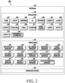
- FIG. 2 is a block diagram 200 illustrating a program 140 according to one or more embodiments.
- the program 140 may include an operating system (OS) 142 to control one or more resources of the electronic device 101, middleware 144, or an application 146 executable on the OS 142.
- the OS 142 may include, for example, Android TM , iOS TM , Windows TM , Symbian TM , Tizen TM , or Bada TM .
- At least part of the program 140 may be pre-loaded on the electronic device 101 (e.g., upon manufacture), or may be downloaded or updated by an external electronic device (e.g., the electronic device 102 or 104 or the server 108) in an environment in which the user uses the electronic device.
- an external electronic device e.g., the electronic device 102 or 104 or the server 108
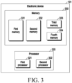
- the third memory 333 may be a volatile memory (e.g., the volatile memory 132 of FIG. 1 ) and may have a lower storage capacity than the first memory 331.
- the third memory 333 may be a static random access memory (SRAM).
- SRAM static random access memory
- the third memory 333 may temporarily store at least a portion of secure data output from the trusted application operating in the trusted application layer 421.
- the trusted application may be executed in the trusted application layer 421 by the second processor 322, and the second processor 322 may temporarily store at least a portion of the secure data generated as the trusted application is executed in the third memory 333 through the secured OS kernel layer 423.
- the fourth memory 334 (e.g., at least a portion of the non-volatile memory 138 of FIG. 1 ) may be a non-volatile memory and may be a secure memory.
- the fourth memory 334 may store at least a portion of secure data output from the trusted application operating in the trusted application layer 421.
- the trusted application may be executed in the trusted application layer 421 by the second processor 322, and the second processor 322 may temporarily store at least a portion of the secure data generated as the trusted application is executed in the fourth memory 334 through the secured OS kernel layer 423.
- the fourth memory 334 may be a storage space in which the functions of reading, modifying, or deleting data are performed infrequently.
- the electronic device 101 may be configured to allow access to the fourth memory 334 only for a specific instruction set. For example, data of the fourth memory 334 may be read, modified, or deleted according to an instruction from the trusted application. Further, data of the fourth memory 334 may not be read, modified, or deleted according to instructions from a general application other than the trusted application. According to one or more embodiments, information used while encrypting the secure data may be stored in the fourth memory 334. Information stored in the fourth memory 334 may be used to decrypt later encrypted secure data. This is described below in greater detail.
- the authority and/or security for the TEE 420 may be higher than the authority and/or security for the REE 410.
- the second processor 322 may access the first memory 331 allocated to the REE 410 from the TEE 420 to read and write data, but the first processor 321 may be restricted from accessing the fourth memory 334 allocated to the TEE 420 in the REE 410.
- the first processor 321 may not be able to write data in the fourth memory 334 or read data stored in the fourth memory 334.
- the REE 410 and the TEE 420 may be allowed to access the second memory 332.
- the electronic device 101 may encrypt the secure data generated by the execution of the trusted application in the TEE 420, store the encrypted secure data in the form of a file in the first memory 331 allocated to the REE 410 through the second memory 332, and store information used to encrypt and/or decrypt the secure data in the fourth memory 334.
- the electronic device 101 may read the encrypted secure data stored in the file form in the first memory 331 allocated to the REE 410 through the currently executed daemon, copy the read secure data in the second memory 332, read secure information used to encrypt and/or decrypt the secure data from the fourth memory 334, decrypt the encrypted secure data copied to the second memory 332 using secure information and temporarily store the decrypted secure data in the third memory 333, and use the decrypted secure data while the trusted application is executed.
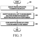
- FIG. 5 is a flowchart 500 illustrating an example of an operation of an electronic device 101 according to one or more embodiments. As understood by one of ordinary skill in the art, the operations shown in FIG. 5 are not limited to the shown order, and may be performed in other various orders. Further, according to one or more embodiments, more or less operations than those of FIG. 5 may be performed. FIG. 5 is described below with reference to FIG. 6 .
- the electronic device 101 may generate secure data by executing the trusted application in the trusted application layer 421 of the TEE 420 in operation 501.
- the generated data may include at least one of information requiring security, such as subscriber identification information, an authentication key, a subscriber phone number, a local area ID, a personal identification number (PIN), and service provider information.
- the secure data may vary depending on the executed application, and may include information designated by the corresponding application developer.
- the electronic device 101 e.g., the second processor 322) may temporarily store secure data (e.g., 631 of FIG. 6 ) generated by executing the trusted application in the third memory 333 through the secured OS kernel layer 423.
- the electronic device 101 may encrypt (e.g., 601 of FIG. 6 ) the secure data, or a portion thereof, being used in the trusted application and may copy (e.g., swap out) the encrypted secure data to the second memory 332 through the secured OS kernel layer 423 (e.g., 621 of FIG. 6 ).
- an advanced encryption standard (AES)-galois/counter mode (GCM) may be used to encrypt data.
- AES advanced encryption standard
- GCM Galois/counter mode
- the encryption method is not limited thereto, and other encryption methods known to one of ordinary skill in the art that guarantee confidentiality and integrity may be used.
- data encryption may be performed in units of blocks obtained by splitting data into predetermined sizes.
- rollback of encrypted data may include changing the encrypted data to a previous form such as unencrypted data.
- an anti-replay counter (ARC) may be used to prevent rollback.
- Different ARC values may be used for each data block to prevent rollback.
- Different ARC values used for each data block may be temporarily stored in the third memory 333 in a table form.
- different ARC values used for each data block may be temporarily stored in the third memory 333 in the form of a table (632 of FIG. 6 ).
- the ARC table may be a linear array composed of ARC values.
- the device specific value is a value unique to the electronic device and may be configured as 4 bytes.
- ARC may be configured as 8 bytes, and IV may be configured as 16 bytes including 4 bytes of zero padding.
- the electronic device 101 may encrypt parameter values generated while encrypting data on a per-block basis and store the encrypted parameter values in the second memory 332 through the secured OS kernel layer 423.
- a tag TAG e.g., 651 of FIG. 6
- the electronic device 101 e.g., the second processor 322 may encrypt the tags generated in the encryption process in the form of a table (e.g., 603 of FIG. 6 ) and store (e.g., swap out) the encrypted tags in the second memory 332 through the secured OS kernel layer 423 (e.g., 623 of FIG. 6 ).
- an electronic code block (AES-ECB) mode may be used to encrypt the tag.
- the encryption method is not limited thereto, and other encryption methods known to one of ordinary skill in the art that guarantee confidentiality may be used.
- the electronic device 101 may encrypt information generated during a data encryption process and stored in the third memory 333, and may copy (e.g., swap out) the encrypted information to the second memory 332 through the secured OS kernel layer 423.
- the electronic device 101 e.g., the second processor 322 may encrypt (e.g., 605 of FIG. 6 ) the ARC table stored in the third memory 333 and may copy (e.g., swap out) the encrypted ARC table to the second memory 332 through the secured OS kernel layer 423 (e.g., 622 of FIG. 6 ).
- AES-GCM may be used to encrypt the ARC table.
- the encryption method is not limited thereto, and other encryption methods known to one of ordinary skill in the art that guarantee confidentiality and integrity may be used.
- the electronic device 101 e.g., the second processor 322 may store the parameters used and generated when encrypting the pieces of information generated in the encryption process in the fourth memory 334 through the secured OS kernel 423.
- the electronic device 101 when encrypting the ARC table, the electronic device 101 (e.g., the second processor 322) may use the master ARC as the initial vector (IV).
- the master ARC may be generated as a random value whenever the secure data generated from the trusted application is stored.
- the master ARC may be used to decrypt the encrypted ARC table.
- the electronic device 101 e.g., the second processor 322 may store the master ARC in the fourth memory 334 through the secured OS kernel layer 423 (e.g., 641 of FIG. 6 ).
- a master tag may be generated while encrypting the ARC table.
- the master tag may be used to decrypt the encrypted ARC table.
- the electronic device 101 e.g., the second processor 322
- the electronic device 101 may store encrypted data stored in the second memory 332 in the first memory 331 allocated to the REE 410.
- the second processor 322 of the electronic device 101 may request the first processor 321 to store the secure data in the first memory 331 allocated to the REE 410 through the mailbox of the secured OS kernel layer 423.
- the first processor 321 of the electronic device 101 may receive the request for secure data from the second processor 322 through the mailbox of the kernel layer 413 while the daemon is being executed in the REE 410.
- the request transmitted from the second processor 322 to the first processor 321 may include the address of the second memory 332 in which the secure data is stored.
- the first processor 321 of the electronic device 101 may read encrypted data stored in the second memory 332 through the daemon running in the REE 410, and may store the encrypted data read through the kernel layer 413 in the first memory 331 (e.g., 607 of FIG. 6 ).
- the encrypted data stored in the second memory 332 may include the encrypted secure data (e.g., 611 of FIG. 6 ), the encrypted ARC table (e.g., 612 of FIG. 6 ), and the encrypted tag table (e.g., 613 of FIG. 6 ), and the encrypted data may be stored in the first memory 331 in the form of one file (e.g., 610 of FIG. 6 ).
- FIG. 7 is a flowchart 700 illustrating an example of an operation of an electronic device 101 according to one or more embodiments. As understood by one of ordinary skill in the art, the operations shown in FIG. 7 are not limited to the shown order , and may be performed in other various orders. Further, according to one or more embodiments, more or less operations than those of FIG. 7 may be performed. FIG. 7 is described below with reference to FIG. 8 .
- the electronic device 101 may execute the trusted application in the trusted application layer 421 of the TEE 420 in operation 701.
- the second processor 322 may request the secure data stored in the first memory 331 from the first processor 321 through the mailbox of the secured OS kernel 423.
- the electronic device 101 may read the encrypted data file (e.g., 610 of FIG. 8 ) stored in the first memory 331 (e.g., 801 of FIG. 8 ).
- the first processor 321 may read the encrypted data file (e.g., 610 of FIG. 8 ) stored in the second memory 332 through the daemon running in the REE 410 (e.g., 801 of FIG. 8 ).
- encrypted data e.g., 611 of FIG. 8
- an encrypted ARC table e.g., 612 of FIG. 8
- an encrypted tag table e.g., 613 of FIG. 8
- the electronic device 101 e.g., the first processor 321 may copy the encrypted data (e.g., 611 of FIG. 8 ), the encrypted ARC table (e.g., 612 of FIG. 8 ), and the encrypted tag table (e.g., 613 of FIG. 8 ) included in the file read from the first memory 331 to the second memory 332.
- the first processor 321 may copy the encrypted data (e.g., 611 of FIG. 8 ), the encrypted ARC table (e.g., 612 of FIG. 8 ), and the encrypted tag table (e.g., 613 of FIG. 8 ) included in a file read from the first memory 331 to the second memory 332 through the daemon running in the REE 410.
- the encrypted data e.g., 611 of FIG. 8
- the encrypted ARC table e.g., 612 of FIG. 8
- the encrypted tag table e.g., 613 of FIG. 8
- the electronic device 101 may decrypt the encrypted data (e.g., 611 of FIG. 8 ) copied to the second memory 332 to be used in the trusted application.
- the electronic device 101 e.g., the second processor 322 may decrypt each of the encrypted data (e.g., 411 of FIG. 6 ), the encrypted ARC table (e.g., 612 of FIG. 8 ), and the encrypted tag table (e.g., 613 of FIG. 8 ).
- the electronic device 101 e.g., the second processor 322) may verify and decrypt the encrypted data generated in the encryption process using the encryption information stored in the fourth memory 334.
- the electronic device 101 may decrypt (e.g., 803 of FIG. 8 ) the encrypted ARC table (e.g., 622 of FIG. 8 ).
- the master ARC e.g., 641 of FIG. 8
- the master tag e.g., 642 of FIG. 8
- the second processor 322 may read the master ARC (e.g., 641 of FIG. 8 ) and the master tag (e.g., 642 of FIG.
- the electronic device 101 may store (e.g., swap in) the decoded ARC table in the third memory 333 through the secured OS kernel layer 423 (e.g., 632 of FIG. 8 ).
- the electronic device 101 may decrypt the encrypted secure data using the decrypted information.
- the electronic device 101 may decrypt the encrypted secure data (e.g., 621 of FIG. 8 ) copied to the second memory 332 on a per-block basis, using the ARC values of the decrypted ARC table (e.g., 632 of FIG. 8 ) and the tag values of the decrypted tag table (e.g., 623 of FIG. 8 ) copied to the second memory 332 (e.g., 805 of FIG. 8 ).
- the data may be divided into one or more blocks, where the data is encrypted in on a per block basis, and subsequently decrypted on the per-block basis.
- the encrypted at least the portion of the secure data stored in the first memory may include an encrypted ARC table 621 storing anti-replay counter ARC values used while encrypting the at least the portion of the secure data on a per-block basis and an encrypted tag table 623 storing tag values generated while encrypting the at least the portion of the secure data on a per-block basis.
- the decrypting 705 may include, by the first processor, decrypting 803 the encrypted ARC table using the first information and the second information, decrypting 805 the tag table, and decrypting 805 the at least the portion of the secure data encrypted on a per-block basis, using the decrypted ARC table and the decrypted tag table.
Landscapes
- Engineering & Computer Science (AREA)
- Computer Security & Cryptography (AREA)
- Theoretical Computer Science (AREA)
- Software Systems (AREA)
- Computer Hardware Design (AREA)
- Physics & Mathematics (AREA)
- General Engineering & Computer Science (AREA)
- General Physics & Mathematics (AREA)
- Computer Networks & Wireless Communication (AREA)
- Signal Processing (AREA)
- General Health & Medical Sciences (AREA)
- Health & Medical Sciences (AREA)
- Bioethics (AREA)
- Telephone Function (AREA)
Applications Claiming Priority (2)
| Application Number | Priority Date | Filing Date | Title |
|---|---|---|---|
| KR1020220160173A KR20240077842A (ko) | 2022-11-25 | 2022-11-25 | 보안 데이터를 저장하는 전자 장치 및 그 동작 방법 |
| PCT/KR2023/018740 WO2024112057A1 (ko) | 2022-11-25 | 2023-11-21 | 보안 데이터를 저장하는 전자 장치 및 그 동작 방법 |
Publications (2)
| Publication Number | Publication Date |
|---|---|
| EP4575871A1 true EP4575871A1 (de) | 2025-06-25 |
| EP4575871A4 EP4575871A4 (de) | 2025-11-12 |
Family
ID=91191363
Family Applications (1)
| Application Number | Title | Priority Date | Filing Date |
|---|---|---|---|
| EP23894985.3A Pending EP4575871A4 (de) | 2022-11-25 | 2023-11-21 | Elektronische vorrichtung zur speicherung sicherer daten und betriebsverfahren dafür |
Country Status (3)
| Country | Link |
|---|---|
| US (1) | US20240178990A1 (de) |
| EP (1) | EP4575871A4 (de) |
| CN (1) | CN120202471A (de) |
Families Citing this family (1)
| Publication number | Priority date | Publication date | Assignee | Title |
|---|---|---|---|---|
| US20240211581A1 (en) * | 2022-12-22 | 2024-06-27 | Micron Technology, Inc. | Contactless data transmission for memory devices |
Family Cites Families (4)
| Publication number | Priority date | Publication date | Assignee | Title |
|---|---|---|---|---|
| US8332653B2 (en) * | 2004-10-22 | 2012-12-11 | Broadcom Corporation | Secure processing environment |
| US20080320263A1 (en) * | 2007-06-20 | 2008-12-25 | Daniel Nemiroff | Method, system, and apparatus for encrypting, integrity, and anti-replay protecting data in non-volatile memory in a fault tolerant manner |
| US11269786B2 (en) * | 2018-07-25 | 2022-03-08 | Intel Corporation | Memory data protection based on authenticated encryption |
| WO2022006535A1 (en) * | 2020-07-02 | 2022-01-06 | SDG Logic Inc. | System and methods for confidential computing |
-
2023
- 2023-11-21 EP EP23894985.3A patent/EP4575871A4/de active Pending
- 2023-11-21 CN CN202380078175.1A patent/CN120202471A/zh active Pending
- 2023-11-27 US US18/520,023 patent/US20240178990A1/en active Pending
Also Published As
| Publication number | Publication date |
|---|---|
| CN120202471A (zh) | 2025-06-24 |
| EP4575871A4 (de) | 2025-11-12 |
| US20240178990A1 (en) | 2024-05-30 |
Similar Documents
| Publication | Publication Date | Title |
|---|---|---|
| US12088694B2 (en) | Method for providing encrypted object and electronic device for supporting the same | |
| KR20220094847A (ko) | 보안 데이터 처리 방법 및 이를 지원하는 전자 장치 | |
| KR102924444B1 (ko) | 액세서리 장치와 무선 통신을 수행하는 전자 장치 및 그 운용 방법 | |
| EP4575871A1 (de) | Elektronische vorrichtung zur speicherung sicherer daten und betriebsverfahren dafür | |
| US20250181705A1 (en) | Electronic device for providing trusted execution environment | |
| EP3896592B1 (de) | Elektronische vorrichtung zur auswahl eines schlüssels zur verschlüsselung auf basis der informationsmenge der zu verschlüsselnden daten und betriebsverfahren für eine elektronische vorrichtung | |
| US20240250833A1 (en) | Electronic device for processing multi-signed apk file, and operating method therefor | |
| EP4543066A1 (de) | Verfahren und vorrichtung zur fernsteuerung einer elektronischen vorrichtung | |
| US12153692B2 (en) | Method of controlling clipboard and electronic device for performing the same | |
| US12277217B2 (en) | Method for application security and electronic device for performing the same | |
| KR20240048449A (ko) | 전자 장치의 원격 제어 방법 및 장치 | |
| KR20240077842A (ko) | 보안 데이터를 저장하는 전자 장치 및 그 동작 방법 | |
| US20260023840A1 (en) | Electronic device for authentication using virtual machine and operation method thereof | |
| KR20220101939A (ko) | 데이터 백업을 지원하는 전자 장치 및 그 운용 방법 | |
| EP4560502A1 (de) | Elektronische vorrichtung und verfahren zur durchführung einer benutzerauthentifizierung auf einer elektronischen vorrichtung | |
| EP4443319A1 (de) | Elektronische vorrichtung zum betrieb einer sicherheitsvorrichtung und betriebsverfahren dafür | |
| US20250208859A1 (en) | Update method and electronic device therefor | |
| US20230070759A1 (en) | Electronic device for protecting user's biometric information | |
| US20260073034A1 (en) | Electronic device for performing subscriber identity module authentication, and operating method and storage medium thereof | |
| EP4580165A1 (de) | Elektronische vorrichtung und kommunikationsverfahren zwischen anwendungen | |
| KR20240047263A (ko) | 신뢰 실행 환경을 제공하기 위한 전자 장치 | |
| KR20240026069A (ko) | 전자 장치 및 전자 장치에서 사용자 인증을 수행하는 방법 | |
| KR20250098787A (ko) | 전자 장치 및 이의 통신 방법 | |
| KR20260001049A (ko) | 임베디드 가입자 식별 모듈을 인증하는 전자 장치, 방법, 및 기록 매체 | |
| KR20250090112A (ko) | 전자 장치 및 전자 장치에서 객체를 관리하기 위한 방법 |
Legal Events
| Date | Code | Title | Description |
|---|---|---|---|
| STAA | Information on the status of an ep patent application or granted ep patent |
Free format text: STATUS: THE INTERNATIONAL PUBLICATION HAS BEEN MADE |
|
| PUAI | Public reference made under article 153(3) epc to a published international application that has entered the european phase |
Free format text: ORIGINAL CODE: 0009012 |
|
| STAA | Information on the status of an ep patent application or granted ep patent |
Free format text: STATUS: REQUEST FOR EXAMINATION WAS MADE |
|
| 17P | Request for examination filed |
Effective date: 20250318 |
|
| AK | Designated contracting states |
Kind code of ref document: A1 Designated state(s): AL AT BE BG CH CY CZ DE DK EE ES FI FR GB GR HR HU IE IS IT LI LT LU LV MC ME MK MT NL NO PL PT RO RS SE SI SK SM TR |
|
| A4 | Supplementary search report drawn up and despatched |
Effective date: 20251014 |
|
| RIC1 | Information provided on ipc code assigned before grant |
Ipc: G06F 21/79 20130101AFI20251008BHEP Ipc: G06F 21/53 20130101ALI20251008BHEP Ipc: G06F 21/60 20130101ALI20251008BHEP Ipc: H04W 12/03 20210101ALI20251008BHEP Ipc: H04L 9/06 20060101ALI20251008BHEP |
|
| DAV | Request for validation of the european patent (deleted) | ||
| DAX | Request for extension of the european patent (deleted) |