EP4575591A1 - Optischer metamaterialbasierter farbkombinierer - Google Patents
Optischer metamaterialbasierter farbkombinierer Download PDFInfo
- Publication number
- EP4575591A1 EP4575591A1 EP23219624.6A EP23219624A EP4575591A1 EP 4575591 A1 EP4575591 A1 EP 4575591A1 EP 23219624 A EP23219624 A EP 23219624A EP 4575591 A1 EP4575591 A1 EP 4575591A1
- Authority
- EP
- European Patent Office
- Prior art keywords
- optical beam
- optical
- collimation
- collimation region
- region
- Prior art date
- Legal status (The legal status is an assumption and is not a legal conclusion. Google has not performed a legal analysis and makes no representation as to the accuracy of the status listed.)
- Pending
Links
Images



Classifications
-
- H—ELECTRICITY
- H10—SEMICONDUCTOR DEVICES; ELECTRIC SOLID-STATE DEVICES NOT OTHERWISE PROVIDED FOR
- H10H—INORGANIC LIGHT-EMITTING SEMICONDUCTOR DEVICES HAVING POTENTIAL BARRIERS
- H10H29/00—Integrated devices, or assemblies of multiple devices, comprising at least one light-emitting semiconductor element covered by group H10H20/00
- H10H29/80—Constructional details
- H10H29/85—Packages
- H10H29/855—Optical field-shaping means, e.g. lenses
-
- G—PHYSICS
- G02—OPTICS
- G02B—OPTICAL ELEMENTS, SYSTEMS OR APPARATUS
- G02B1/00—Optical elements characterised by the material of which they are made; Optical coatings for optical elements
- G02B1/002—Optical elements characterised by the material of which they are made; Optical coatings for optical elements made of materials engineered to provide properties not available in nature, e.g. metamaterials
-
- G—PHYSICS
- G02—OPTICS
- G02B—OPTICAL ELEMENTS, SYSTEMS OR APPARATUS
- G02B19/00—Condensers, e.g. light collectors or similar non-imaging optics
- G02B19/0033—Condensers, e.g. light collectors or similar non-imaging optics characterised by the use
- G02B19/0047—Condensers, e.g. light collectors or similar non-imaging optics characterised by the use for use with a light source
- G02B19/0061—Condensers, e.g. light collectors or similar non-imaging optics characterised by the use for use with a light source the light source comprising a LED
- G02B19/0066—Condensers, e.g. light collectors or similar non-imaging optics characterised by the use for use with a light source the light source comprising a LED in the form of an LED array
-
- G—PHYSICS
- G02—OPTICS
- G02B—OPTICAL ELEMENTS, SYSTEMS OR APPARATUS
- G02B27/00—Optical systems or apparatus not provided for by any of the groups G02B1/00 - G02B26/00, G02B30/00
- G02B27/10—Beam splitting or combining systems
- G02B27/1006—Beam splitting or combining systems for splitting or combining different wavelengths
-
- G—PHYSICS
- G02—OPTICS
- G02B—OPTICAL ELEMENTS, SYSTEMS OR APPARATUS
- G02B27/00—Optical systems or apparatus not provided for by any of the groups G02B1/00 - G02B26/00, G02B30/00
- G02B27/30—Collimators
-
- G—PHYSICS
- G02—OPTICS
- G02B—OPTICAL ELEMENTS, SYSTEMS OR APPARATUS
- G02B5/00—Optical elements other than lenses
- G02B5/18—Diffraction gratings
- G02B5/1809—Diffraction gratings with pitch less than or comparable to the wavelength
Definitions
- the present disclosure relates to the collimation of optical beams generated by an array of emission pixels.
- the disclosure proposes an integrated optical system.
- the optical system comprises an array of emission pixels that generate optical beams which are collimated.
- an objective of this disclosure is to improve the pixel density and/or the visualization quality of optical systems.
- an objective is to improve the brightness and pixel pitch of said optical systems by improving optical beam gathering in high-pixel-density displays.
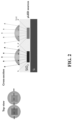
- FIG. 2 shows conventional collimation lenses.
- collimating lenses can be placed above the light sources.
- conventional collimating lenses cannot capture light emitted at wide angles. Due to the size constraints in small-pixel-pitch displays, lens arrays that can be fabricated above the light sources cannot effectively capture all of the light, and certain portions are inevitably lost, for example, the outer rays shown in FIG. 2 . Hence, the brightness is reduced due to the incomplete light gathering in high-pixel-density displays.
- the emerging ⁇ LED technology based on compound semiconductors may be a promising candidate to deliver the necessary pixel density and luminosity required for, for example, AR and VR displays.
- a first aspect of this disclosure provides an integrated optical system comprising: an array of emission pixels, each emission pixel being configured to emit a respective optical beam having a respective wavelength, a controller configured to control the array of emission pixels to emit two or more optical beams by using two or more emission pixels, and an optical metamaterial having a plurality of subwavelength structures, wherein the plurality of subwavelength structures comprises at least two distinct materials having different refractive indices, wherein the optical metamaterial comprises a plurality of collimation regions, each collimation region being associated with one respective emission pixel of the array of emission pixels, wherein the plurality of collimation regions are arranged to receive the two or more optical beams from the array of emission pixels, and wherein a first collimation region of the plurality of collimation regions is configured to collimate respectively a first part of a first optical beam of the two or more optical beams and a second part of a second optical beam of the two or more optical beams by diffracting the first part of the first optical beam and the second part of the
- Collimating said parts of the first optical beam and the second optical beam may further comprise refracting said parts based on the refractive indices of the at least two materials.
- the plurality of subwavelength structures may be formed or defined by a physical distribution of the at least two distinct materials in the metamaterial, wherein each subwavelength structure may comprise one, for example, only one, distinct material of the at least two distinct materials.
- a first material of the at least two distinct materials that, for example, forms a first material island, and is surrounded by at least a second material of the at least two distinct materials may be considered to be a first subwavelength structure of the plurality of subwavelength structures.
- the second material of the at least two distinct materials that, for example, forms a second material island, and is surrounded by at least the first material may be considered to be a second subwavelength structure of the plurality of subwavelength structures.
- the at least two distinct materials may comprise at least one of Si 3 N 4 , SiO 2 , and TiO 2 .
- Each subwavelength structure of the plurality of subwavelength structures may or may not have an abstract shape.
- Said shapes may be respectively one-dimensional, two-dimensional, or three-dimensional.
- the plurality of collimation regions may be non-overlapping.
- the first collimation region and the second collimation region may be non-overlapping.
- the first collimation region and the second collimation region may be adjacent, for example directly adjacent.
- the plurality of collimation regions may be a one-dimensional or a two-dimensional array of collimation regions.
- the plurality of collimation regions may be arranged regularly, for example, having the same distances between collimation regions, or irregularly.
- the arrangement of the array of emission pixels may define a first plane and an arrangement of the plurality of collimation regions may define a second plane, wherein the first plane and the second plane may be parallel to each other.
- Each optical beam of the two or more optical beams may be monochromatic.
- Each emission pixel of the array of emission pixels may be configured to emit a respective monochromatic optical beam having a respective wavelength.
- the optical system may comprise a display, for example a micro light-emitting diode (LED) display.
- the display may comprise the array of emission pixels.
- the display may or may not comprise the metamaterial.
- the term 'integrated' in the context of the optical system may denote a cohesive design where various optical components, for example, optical beam sources, lenses, collimation regions, and detectors, are combined into a unified assembly.
- This integration for example, achieved through monolithic or hybrid methods, may enhance the system's functionality. It may offer advantages such as miniaturization, improved reliability, and cost efficiency. Specifically, for a system with a pixel array emitting optical beams, this integration may allow for precise optical beam control at the pixel level, potentially enhancing imaging or communication applications.
- the term 'integrated' covers various design approaches, emphasizing flexibility and efficiency in the optical system's operation.
- different emission pixels can be used to emit optical beams having different wavelengths.
- the two optical beams having different wavelengths can be then collimated into two collimated beams by one collimation region that is associated with one emission pixel.
- the two optical beams having different wavelengths can further be collimated into the two collimated beams by another collimation region.
- the brightness can be increased and/or a high-density array of emission pixels can be used without the above mentioned drawbacks.
- each collimation region of the plurality of collimation regions is centered above the respective emission pixel that is associated with the collimation region.
- the respective emission pixel that is associated with the first collimation region may be a first emission pixel.
- the respective emission pixel that is associated with the second collimation region may be a second emission pixel.
- the two or more optical beams may be three or more optical beams and may comprise a third optical beam.
- the first collimation region may be further configured to collimate a second part of a third optical beam, by diffracting the second part of the third optical beam based on the distribution of the plurality of subwavelength structures in the first collimation region.
- the second part of the third optical beam may thereby be combined with a first part of the third optical beam to form at least a part of a third collimated optical beam.
- the third optical beam may be generated by a third emission pixel that is associated with a third collimation region of the plurality of collimation regions.
- the third emission pixel may be adjacent, for example, directly adjacent, to the first emission pixel.
- the third optical beam and the first optical beam may or may not have the same wavelength, for example, the same central wavelength or the same entire frequency spectrum.
- the first optical beam and the third optical beam may have different angles of incidence on the first collimation region.
- Collimating said parts of the third optical beam may further comprise refracting said parts based on the refractive indices of the at least two materials.
- the plurality of collimation regions are arranged such that, for each emission pixel of the array of emission pixels, the respective optical beam emitted by the respective emission pixel is primarily collimated by the collimation region that is associated with the respective emission pixel.
- the first optical beam may be primarily collimated by the first collimation region.
- the second collimation region may be primarily collimated by the second collimation region.
- the third collimation region may be primarily collimated by the third collimation region.
- the term primarily may refer to, for example, a majority of the first optical beam being collimated by the first collimation region.
- the term majority or the term primarily may refer to a majority of the optical power of an optical beam, for example, the first optical beam, being collimated by a respective collimation region, for example, the first collimation region.
- the plurality of collimation regions are arranged such that the first part of the first optical beam and the second part of the second optical beam have different angles of incidence on the first collimation region.
- the distribution of the plurality subwavelength structures in the first collimation region may be configured based on said different angles of incidence.
- the plurality of collimation regions are arranged such that the second part of the first optical beam and the first part of the second optical beam have different angles of incidence on the second collimation region.
- the distribution of the plurality subwavelength structures in the second collimation region may be configured based on said different angles of incidence.
- the distribution of the plurality of subwavelength structures in the first collimation region and/or the refractive indices of the at least two distinct materials is/are configured based on estimated respective angles of incidence of the first part of the first optical beam and the second part of the second optical beam on the first collimation region.
- Said angles of incidence may be estimated based on: (i) the geometric relationship between the first emission pixel and the first collimation region, (ii) the geometric relationship second emission pixel and the first collimation region, (iii) an emission angle of the first emission pixel, and (iv) an emission angle of the second emission pixel.
- the distribution of the plurality of subwavelength structures in the second collimation region and/or the refractive indices of the at least two distinct materials is/are configured based on estimated respective angles of incidence of the first part of the second optical beam and the second part of the first optical beam on the second collimation region.
- Said angles of incidence may be estimated based on: (i) the geometric relationship between the first emission pixel and the second collimation region, (ii) the geometric relationship second emission pixel and the second collimation region, (iii) an emission angle of the first emission pixel, and (iv) an emission angle of the second emission pixel.
- angles of incidence may be estimated based on the geometric relationship between the array of emission pixels and the plurality of collimation regions.
- every part of the two or more optical beams that the first collimation region receives may be collimated, for example, respectively collimated.
- the second collimation region is arranged to receive only the first part of the second optical beam and only the second part of the first optical beam.
- every part of the two or more optical beams that the second collimation region receives may be collimated, for example, respectively collimated.
- the metamaterial may efficiently collimate the two or more optical beams, for example, the first optical beam and the second optical beam.
- the plurality of collimation regions are arranged abuttingly.
- the plurality of collimation regions may be non-overlapping.
- the optical system can be flexibly fabricated for additional applications.
- an application of the optical system may have high requirements in terms of size such that directly providing the collimated beams into a predefined direction may be required.
- a first element and a second element are considered to be different elements, if not explicitly mentioned otherwise.
- the first optical beam and the second optical beam are considered to be different optical beams, they are at least different because of the different frequency, but further also as they form part of different optical beams emitted by different emission pixels.
- the first part of the first optical beam and the second part of the first optical beam are considered to be different parts of the first optical beam.
- the first part of the second optical beam and the second part of the second optical beam are considered to be different parts of the second optical beam.
- the first collimation region and the second collimation region are considered to be different collimation regions.
- Optical metamaterials comprise subwavelength structures, typically made of at least two materials of distinct refractive indices. Optical metamaterials can be used to manipulate intensity, phase or polarization of optical beams.
- FIG. 3 shows a cross-section of an optical system 100 according to this disclosure.
- the optical system 100 for example, the optical system 100 shown in FIG. 1 , comprises a metamaterial 103, which comprises a plurality of subwavelength structures 104.
- an intermediate layer 111 comprising SiO 2 is provided on the array of emission pixels 101, wherein the metamaterial 103 is provided on the intermediate layer 111, and wherein the intermediate layer 111 and/or the array of emission pixels 101 are provide on the substrate 112, which comprises Si.
- the controller 102 is not shown.
- FIG. 3 shows an exemplary first optical beam 107 generated by a first emission pixel 101a, and an exemplary second optical beam 108 generated by a second emission pixel 101b.
- the area occupied by the first optical beam 107 and the area occupied by the second optical beam 108 is respectively indicated by arrows extending form the first emission pixel 101a and the second emission pixel 101b, wherein respectively the arrows located at the most outer positions respectively indicate the boundaries of the respective beams.
- the metamaterial 103 can be divided or partitioned, for example, conceptually divided, into a plurality of collimation regions 105.
- the division of the metamaterial 103 into a first collimation region 105a and a second collimation region 105b is indicated by dashed boxes in FIG. 3 .
- FIG. 3 shows that the outer parts of the first optical beam 107 and the outer parts of the second optical beam 108 spatially overlap at the plurality of collimation regions 105, which is indicated by the arrows located at the most outer positions.
- the first collimation region 105a receives a second part 108b of the second optical beam 108 and the second collimation region 105b receives a second part 107b of the first optical beam 107.
- FIG. 3 shows that the majority of the first optical beam 107 or a first part 107a of the first optical beam 107 is received by the first collimation region 105a, wherein the majority of the second optical beam 108 or a first part 108a of the second optical beam 108 is received by the second collimation region 105b.
- a part of the first collimation region 105a that receives the first part 107a of the first optical beam 107 and the second part 108b of the second optical beam 108, for example, the part of the first collimation region 105a where said parts overlap, may be configured to collimate both of said parts 107a, 108b of the optical beams 107, 108.
- a part of the second collimation region 105b that receives the first part 108a of the second optical beam 108 and the second part 107b of the first optical beam 107 may be configured to collimate both of said parts 108a, 107b of the optical beams 107, 108.
- FIG. 3 shows that the first part 107a of the first optical beam 107 and the second part 107b of the first optical beam 107 are combined into at least a part of a first collimated optical beam 109, and that the first part 108a of the second optical beam 108 and the second part 108b of the second optical beam 108 are combined into at least a part of a second collimated optical beam 110.
- FIG. 4 shows an exemplary metamaterial 103 according to this disclosure.
- FIG. 4 shows exemplary materials of the at least two distinct materials, wherein Si 3 N 4 is shown in grey and TiO 2 is shown in black.
- the disclosure and scope of the claims is however not limited thereto, the skilled person will recognize there exist other materials systems/combinations that can be used to obtain the same effect.
- the distribution formed by the subwavelength structures in each collimation region may be irregular as shown in the exemplary distribution of FIG. 4 .
- the distribution may comprise tuned periodicities for the two or more optical beams.
- the metamaterial 103 comprises four layers, wherein the distribution of the plurality of subwavelength structures 104 was formed based on a machine learning algorithm.
- a computer implemented algorithm for example, a machine learning algorithm, may consider the requirements for collimating respective parts of optical beams that are supposed to be collimated by the metamaterial 103 at each positions and determine the distribution of the plurality of subwavelength structures 104 in the metamaterial 103 based on said requirements.
- the metamaterial 103 may be considered to be an implementation of partially overlapping lenses, each lens forming a collimated optical beam from an associated set of adjacent emission pixels, each pixel emitting an optical beam of a unique wavelength, each lens thereby forming a collimated optical beam for that specific wavelength of the optical beam.
Landscapes
- Physics & Mathematics (AREA)
- General Physics & Mathematics (AREA)
- Optics & Photonics (AREA)
- Optical Elements Other Than Lenses (AREA)
Priority Applications (2)
| Application Number | Priority Date | Filing Date | Title |
|---|---|---|---|
| EP23219624.6A EP4575591A1 (de) | 2023-12-22 | 2023-12-22 | Optischer metamaterialbasierter farbkombinierer |
| US18/987,436 US20250212589A1 (en) | 2023-12-22 | 2024-12-19 | Optical metamaterial-based color combiner |
Applications Claiming Priority (1)
| Application Number | Priority Date | Filing Date | Title |
|---|---|---|---|
| EP23219624.6A EP4575591A1 (de) | 2023-12-22 | 2023-12-22 | Optischer metamaterialbasierter farbkombinierer |
Publications (1)
| Publication Number | Publication Date |
|---|---|
| EP4575591A1 true EP4575591A1 (de) | 2025-06-25 |
Family
ID=89430303
Family Applications (1)
| Application Number | Title | Priority Date | Filing Date |
|---|---|---|---|
| EP23219624.6A Pending EP4575591A1 (de) | 2023-12-22 | 2023-12-22 | Optischer metamaterialbasierter farbkombinierer |
Country Status (2)
| Country | Link |
|---|---|
| US (1) | US20250212589A1 (de) |
| EP (1) | EP4575591A1 (de) |
Citations (7)
| Publication number | Priority date | Publication date | Assignee | Title |
|---|---|---|---|---|
| US20180284428A1 (en) * | 2017-03-29 | 2018-10-04 | Microsoft Technology Licensing, Llc | Achromatized metasurface lens |
| US20200004020A1 (en) * | 2018-06-28 | 2020-01-02 | Apple Inc. | Electronic Device With Multi-Element Display Illumination System |
| US20220100070A1 (en) * | 2019-01-10 | 2022-03-31 | Osram Gmbh | Image displaying device and method for displaying an image on a screen |
| US20220102583A1 (en) * | 2019-01-29 | 2022-03-31 | Osram Opto Semiconductors Gmbh | µ-LED, µ-LED DEVICE, DISPLAY AND METHOD FOR THE SAME |
| US20220299760A1 (en) * | 2016-04-29 | 2022-09-22 | The Board Of Trustees Of The Leland Stanford Junior University | Device components formed of geometric structures |
| WO2022271430A1 (en) * | 2021-06-22 | 2022-12-29 | Google Llc | Display systems using light extraction configurations for micro light emitting diodes |
| WO2023164065A1 (en) * | 2022-02-25 | 2023-08-31 | Hes Ip Holdings, Llc | Optical assembly for head wearable displays |
-
2023
- 2023-12-22 EP EP23219624.6A patent/EP4575591A1/de active Pending
-
2024
- 2024-12-19 US US18/987,436 patent/US20250212589A1/en active Pending
Patent Citations (7)
| Publication number | Priority date | Publication date | Assignee | Title |
|---|---|---|---|---|
| US20220299760A1 (en) * | 2016-04-29 | 2022-09-22 | The Board Of Trustees Of The Leland Stanford Junior University | Device components formed of geometric structures |
| US20180284428A1 (en) * | 2017-03-29 | 2018-10-04 | Microsoft Technology Licensing, Llc | Achromatized metasurface lens |
| US20200004020A1 (en) * | 2018-06-28 | 2020-01-02 | Apple Inc. | Electronic Device With Multi-Element Display Illumination System |
| US20220100070A1 (en) * | 2019-01-10 | 2022-03-31 | Osram Gmbh | Image displaying device and method for displaying an image on a screen |
| US20220102583A1 (en) * | 2019-01-29 | 2022-03-31 | Osram Opto Semiconductors Gmbh | µ-LED, µ-LED DEVICE, DISPLAY AND METHOD FOR THE SAME |
| WO2022271430A1 (en) * | 2021-06-22 | 2022-12-29 | Google Llc | Display systems using light extraction configurations for micro light emitting diodes |
| WO2023164065A1 (en) * | 2022-02-25 | 2023-08-31 | Hes Ip Holdings, Llc | Optical assembly for head wearable displays |
Non-Patent Citations (3)
| Title |
|---|
| F. AIETA ET AL: "Multiwavelength achromatic metasurfaces by dispersive phase compensation", SCIENCE, vol. 347, no. 6228, 20 March 2015 (2015-03-20), US, pages 1342 - 1345, XP055432399, ISSN: 0036-8075, DOI: 10.1126/science.aaa2494 * |
| LIU ZEYANG ET AL: "Metasurface-enabled augmented reality display: a review", ADVANCED PHOTONICS SPIE USA, SOCIETY OF PHOTO-OPTICAL INSTRUMENTATION ENGINEERS, 1000 20TH ST. BELLINGHAM WA 98225-6705 USA, vol. 5, no. 3, 1 May 2023 (2023-05-01), pages 34001, XP060183612, ISSN: 2577-5421, [retrieved on 20230515], DOI: 10.1117/1.AP.5.3.034001 * |
| YAN LI: "Metasurfaces for near-eye display applications", OPTO-ELECTRONIC SCIENCE, vol. 2, no. 8, 31 October 2023 (2023-10-31), pages 230025 - 230025, XP093160701, ISSN: 2097-0382, Retrieved from the Internet <URL:https://www.oejournal.org/oej-data/oes/2023/8/PDF/oes-2023-0025.pdf> DOI: 10.29026/oes.2023.230025 * |
Also Published As
| Publication number | Publication date |
|---|---|
| US20250212589A1 (en) | 2025-06-26 |
Similar Documents
| Publication | Publication Date | Title |
|---|---|---|
| US11675199B1 (en) | Systems, devices, and methods for tiled multi-monochromatic displays | |
| CN102608762B (zh) | 图像显示装置 | |
| JP7769705B2 (ja) | 非メガネ方式の3d表示装置 | |
| US12009465B1 (en) | LED array having transparent substrate with conductive layer for enhanced current spread | |
| US12189280B2 (en) | Lighting arrangement, light guide arrangement and method | |
| US12572055B2 (en) | Microlens array with built-in air gap | |
| KR20200079904A (ko) | 표시장치 | |
| US12422676B2 (en) | Eye tracking head mounted display device | |
| KR20180045319A (ko) | 지향성 백라이트 유닛 및 이를 포함하는 입체 영상 표시 장치 | |
| EP4575591A1 (de) | Optischer metamaterialbasierter farbkombinierer | |
| US20250234685A1 (en) | Micron-scale light-emitting device with reduced-area central anode contact | |
| US20200049979A1 (en) | Scanning display with increased uniformity | |
| JP2025505060A (ja) | マイクロled表示デバイス | |
| CN214751131U (zh) | 裸眼三维显示装置 | |
| US20220043268A1 (en) | Display device | |
| TWI475298B (zh) | Time - based energy - saving color separation system | |
| US20240332343A1 (en) | Reducing crosstalk and improving contrast in led and pcled arrays | |
| US20250280646A1 (en) | TRANSPARENT STRUCTURE ON pcLED TO INCREASE LIGHT FLUX | |
| US20250271116A1 (en) | Microled and microlens assembly | |
| WO2024129205A1 (en) | High transmission large area metalenses | |
| US20250169250A1 (en) | Light-emitting diode with spectrally selective optical element | |
| WO2024123425A1 (en) | Led device with protection layer and method of manufacturing the same | |
| KR20230097948A (ko) | 디스플레이 패널 및 이를 채용한 디스플레이 장치 | |
| KR20210028931A (ko) | 헤드 마운트 디스플레이장치 |
Legal Events
| Date | Code | Title | Description |
|---|---|---|---|
| PUAI | Public reference made under article 153(3) epc to a published international application that has entered the european phase |
Free format text: ORIGINAL CODE: 0009012 |
|
| STAA | Information on the status of an ep patent application or granted ep patent |
Free format text: STATUS: THE APPLICATION HAS BEEN PUBLISHED |
|
| AK | Designated contracting states |
Kind code of ref document: A1 Designated state(s): AL AT BE BG CH CY CZ DE DK EE ES FI FR GB GR HR HU IE IS IT LI LT LU LV MC ME MK MT NL NO PL PT RO RS SE SI SK SM TR |
|
| STAA | Information on the status of an ep patent application or granted ep patent |
Free format text: STATUS: REQUEST FOR EXAMINATION WAS MADE |
|
| 17P | Request for examination filed |
Effective date: 20251209 |