EP4574748A1 - Process for manufacturing microelectromechanical devices with chambers sealed at different pressures and microelectromechanical device thereby manufactured - Google Patents
Process for manufacturing microelectromechanical devices with chambers sealed at different pressures and microelectromechanical device thereby manufactured Download PDFInfo
- Publication number
- EP4574748A1 EP4574748A1 EP24216750.0A EP24216750A EP4574748A1 EP 4574748 A1 EP4574748 A1 EP 4574748A1 EP 24216750 A EP24216750 A EP 24216750A EP 4574748 A1 EP4574748 A1 EP 4574748A1
- Authority
- EP
- European Patent Office
- Prior art keywords
- layer
- cavity
- substrate
- chamber
- dielectric layer
- Prior art date
- Legal status (The legal status is an assumption and is not a legal conclusion. Google has not performed a legal analysis and makes no representation as to the accuracy of the status listed.)
- Pending
Links
Images







Classifications
-
- B—PERFORMING OPERATIONS; TRANSPORTING
- B81—MICROSTRUCTURAL TECHNOLOGY
- B81B—MICROSTRUCTURAL DEVICES OR SYSTEMS, e.g. MICROMECHANICAL DEVICES
- B81B7/00—Microstructural systems ; Auxiliary parts of microstructural devices or systems
- B81B7/02—Microstructural systems ; Auxiliary parts of microstructural devices or systems containing distinct electrical or optical devices of particular relevance for their function, e.g. microelectro-mechanical systems [MEMS]
-
- B—PERFORMING OPERATIONS; TRANSPORTING
- B81—MICROSTRUCTURAL TECHNOLOGY
- B81B—MICROSTRUCTURAL DEVICES OR SYSTEMS, e.g. MICROMECHANICAL DEVICES
- B81B7/00—Microstructural systems ; Auxiliary parts of microstructural devices or systems
- B81B7/0032—Packages or encapsulation
- B81B7/0035—Packages or encapsulation for maintaining a controlled atmosphere inside of the chamber containing the MEMS
- B81B7/0041—Packages or encapsulation for maintaining a controlled atmosphere inside of the chamber containing the MEMS maintaining a controlled atmosphere with techniques not provided for in B81B7/0038
-
- B—PERFORMING OPERATIONS; TRANSPORTING
- B81—MICROSTRUCTURAL TECHNOLOGY
- B81C—PROCESSES OR APPARATUS SPECIALLY ADAPTED FOR THE MANUFACTURE OR TREATMENT OF MICROSTRUCTURAL DEVICES OR SYSTEMS
- B81C1/00—Manufacture or treatment of devices or systems in or on a substrate
- B81C1/00015—Manufacture or treatment of devices or systems in or on a substrate for manufacturing microsystems
- B81C1/00261—Processes for packaging MEMS devices
- B81C1/00277—Processes for packaging MEMS devices for maintaining a controlled atmosphere inside of the cavity containing the MEMS
- B81C1/00293—Processes for packaging MEMS devices for maintaining a controlled atmosphere inside of the cavity containing the MEMS maintaining a controlled atmosphere with processes not provided for in B81C1/00285
-
- B—PERFORMING OPERATIONS; TRANSPORTING
- B81—MICROSTRUCTURAL TECHNOLOGY
- B81B—MICROSTRUCTURAL DEVICES OR SYSTEMS, e.g. MICROMECHANICAL DEVICES
- B81B2201/00—Specific applications of microelectromechanical systems
- B81B2201/02—Sensors
- B81B2201/0228—Inertial sensors
- B81B2201/0235—Accelerometers
-
- B—PERFORMING OPERATIONS; TRANSPORTING
- B81—MICROSTRUCTURAL TECHNOLOGY
- B81B—MICROSTRUCTURAL DEVICES OR SYSTEMS, e.g. MICROMECHANICAL DEVICES
- B81B2201/00—Specific applications of microelectromechanical systems
- B81B2201/02—Sensors
- B81B2201/0228—Inertial sensors
- B81B2201/0242—Gyroscopes
-
- B—PERFORMING OPERATIONS; TRANSPORTING
- B81—MICROSTRUCTURAL TECHNOLOGY
- B81B—MICROSTRUCTURAL DEVICES OR SYSTEMS, e.g. MICROMECHANICAL DEVICES
- B81B2203/00—Basic microelectromechanical structures
- B81B2203/03—Static structures
- B81B2203/0307—Anchors
-
- B—PERFORMING OPERATIONS; TRANSPORTING
- B81—MICROSTRUCTURAL TECHNOLOGY
- B81B—MICROSTRUCTURAL DEVICES OR SYSTEMS, e.g. MICROMECHANICAL DEVICES
- B81B2203/00—Basic microelectromechanical structures
- B81B2203/03—Static structures
- B81B2203/0315—Cavities
-
- B—PERFORMING OPERATIONS; TRANSPORTING
- B81—MICROSTRUCTURAL TECHNOLOGY
- B81C—PROCESSES OR APPARATUS SPECIALLY ADAPTED FOR THE MANUFACTURE OR TREATMENT OF MICROSTRUCTURAL DEVICES OR SYSTEMS
- B81C2203/00—Forming microstructural systems
- B81C2203/01—Packaging MEMS
- B81C2203/0118—Bonding a wafer on the substrate, i.e. where the cap consists of another wafer
-
- B—PERFORMING OPERATIONS; TRANSPORTING
- B81—MICROSTRUCTURAL TECHNOLOGY
- B81C—PROCESSES OR APPARATUS SPECIALLY ADAPTED FOR THE MANUFACTURE OR TREATMENT OF MICROSTRUCTURAL DEVICES OR SYSTEMS
- B81C2203/00—Forming microstructural systems
- B81C2203/01—Packaging MEMS
- B81C2203/0172—Seals
- B81C2203/019—Seals characterised by the material or arrangement of seals between parts
Definitions
- the present invention relates to a process for manufacturing microelectromechanical devices with chambers sealed at different pressures and a microelectromechanical device thereby manufactured.
- the devices may have optimal operating conditions very different from each other, as in the case of gyroscopes and accelerometers.
- the gyroscopes work in an environment having low pressure, typically comprised between 0.1 mbar and 1 mbar.
- the gyroscopes are maintained constantly oscillating in resonance and low-pressure conditions allow the maintenance of the oscillations, reducing damping and dissipated energy.
- Accelerometers on the other hand, normally operate under higher pressure conditions, for example between 1 mbar and a few atmospheres. Similar issues also arise with other types of devices operating under different conditions, for example resonators, wake-up systems, geophones or bolometers in combination with gyroscopes or accelerometers.
- a possible solution consists in including different devices in a same cavity or chamber of the package, wherein a pressure level corresponding to a trade-off between the preferred operating pressures is present. Solutions of this type are relatively simple to implement but may be unsatisfactory and affect performance.
- the microelectromechanical devices are included in respective sealed and non-communicating chambers.
- the devices for example gyroscopes and accelerometers, are manufactured in a first wafer, while, in a second wafer, caps are provided, and cavities are formed in positions corresponding to respective sensors.
- a layer of an absorbent material or getter is also deposited.
- the getter is thermally activated and absorbs the non-noble gases present in the chamber, reducing pressure. In this manner chambers sealed at different pressures may be obtained and all the devices may operate under preferred pressure conditions.
- the amount of available gaseous nitrogen may saturate the getter and, in this case, the pressure target in the chamber may not be achieved.
- the dimensions (base area and/or height) of the chamber may be greater than what would be sufficient for the sole microelectromechanical devices.
- the getter may be activated prematurely during the wafer bonding steps, before the chambers are completely sealed.
- the getter may also absorb gas from the higher-pressure chamber (cross-talk), creating a double drawback.
- cross-talk higher-pressure chamber
- the pressure of the getter-free chamber decreases and in any case the final pressure value is not accurately predictable.
- the getter may more easily saturate and therefore even in the low-pressure chamber the atmosphere may not reach the desired level.
- US 2014/117472 A1 discloses a microelectromechanical device and a process for manufacturing microelectromechanical devices.
- the microelectromechanical device disclosed in US 2014/117472 A1 comprises a substrate of semiconductor material; a dielectric layer on the substrate; a structural layer of semiconductor material on the dielectric layer; in the structural layer, a first microelectromechanical device and a second microelectromechanical device sealed respectively in a first chamber at a first pressure and in a second chamber at a second pressure, different from the first pressure; a channel traversing the substrate; in the dielectric layer, a first cavity fluidically coupled to the channel, a second cavity fluidically coupled to the first chamber and a fluidic passage between the first cavity and the second cavity; and a sealing layer that closes the fluidic passage and fluidically isolates the first cavity from the second cavity.
- a dielectric layer and a structural layer are formed on a first semiconductor wafer having a substrate of semiconductor material, the substrate being selectively etchable with respect to the stop layer.
- a first microelectromechanical device and a second microelectromechanical device are formed in the structural layer and are sealed respectively in a first chamber and a second chamber at a first pressure.
- the first chamber is fluidically coupled to an external environment through the substrate and is sealed at a second pressure different from the first pressure.
- a cavity fluidically coupled to the first chamber in the dielectric layer and a channel are formed.
- microelectromechanical devices and processes to manufacture microelectromechanical devices are disclosed in US 2015/123217 A1 and US 2014/306300 A1 .
- a semiconductor wafer 1 comprises a substrate 2, for example of monocrystalline silicon.
- the wafer 1 is intended to accommodate microstructures of microelectromechanical devices and hereinafter it will be referred to as microstructure wafer 1. More in detail, a first region of the microstructure wafer 1, indicated by 1a, is intended to accommodate a first microelectromechanical sensor operating at a first pressure, for example a gyroscope, and a second region of the microstructure wafer 1, indicated by 1b, is intended to accommodate a second microelectromechanical sensor operating at a second pressure, higher than the first pressure, for example an accelerometer.
- a first pressure for example a gyroscope
- a second region of the microstructure wafer 1, indicated by 1b is intended to accommodate a second microelectromechanical sensor operating at a second pressure, higher than the first pressure, for example an accelerometer.
- other microelectromechanical devices that require different operating pressures, such as resonators and wake-up systems, may be
- first trenches 5 extend continuously along respective closed paths nested one inside the other. In the embodiment described herein, in particular two circular and concentric first trenches 5 are opened.
- the second trenches 6 are enclosed inside the first trenches 5 and, in one embodiment, are organized in arrays which extend on closed paths L1, ..., LN (three in the illustrated example) nested one in the other.
- the closed paths are concentric circumferences and each second trench 6 extends on a portion of a respective closed path L1, ..., LN.
- Second trenches 6 which extend along a same closed path are separated from each other by portions of the dielectric layer 3.
- a first region 3a and a second region 3b of the dielectric layer 3 respectively internal to the second trenches 6 and comprised between the first trenches 5 and the second trenches 6, are connected to each other through the portions of the dielectric layer 3 which separate consecutive second trenches 6.
- second trenches might not be organized in closed paths and might otherwise be arranged to form anchors, according to design preferences.
- the second trenches here indicated by 6', are aligned in rows.
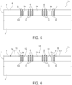
- the microstructure wafer 1 is then covered with a stop layer 7 ( Figure 5 ), thin enough to coat the inside of the first trenches 5 and the second trenches 6 without filling them.
- the stop layer 7 is of a material with respect to which the silicon (or, in general, the material forming the substrate 2) is selectively etchable, for example alumina.
- a connection and anchoring layer 8 for example of polycrystalline silicon, is deposited on the microstructure wafer 1 and fills the first trenches 5 and the second trenches 6 forming anchoring rings 10 and anchoring pins 11 respectively, in this case with portions of the stop layer 7 which coat the inside of the first trenches 5 and the second trenches 6.
- the anchoring pins 11, in particular, are organized in concentric arrays, corresponding to respective closed paths L1, ..., LN. In each array, adjacent anchoring pins 11 are separated by portions of the dielectric layer 3.
- the dimensions of the second trenches 6 and the distances between consecutive second trenches 6 at least of the innermost array are selected so that the spaces between consecutive anchoring pins 11 may be sealed by a plasma deposition process, as detailed below.
- the spacing between consecutive anchoring pins 11 may be between 1 ⁇ m and 5 ⁇ m.
- the stop layer 7 and the connection and anchoring layer 8 are defined to open one or more windows 12 between the first region 3a of the dielectric layer 3 and the innermost of the anchoring rings 10 (which corresponds to the innermost of the first trenches 5), so as to expose part of the dielectric layer 3.
- a single window 12 having annular shape is opened on the second region 3b of the dielectric layer 3. Consequently, a crown portion of the dielectric layer 3, of a shape corresponding to the window 12, is exposed.
- a plurality of windows may be opened, for example circular and distributed along a circumference.
- anchoring pad 13 In a zone radially internal to the window 12, or more precisely over the first portion 3a of the dielectric layer 3 and over the anchoring pins 11 up to an inner edge of the window 12, remaining portions of the connection and anchoring layer 8 form an anchoring pad 13 bonded to the anchoring pins 11.
- the anchoring pad 13 forms an anchoring structure 15 with the anchoring pins 11.
- the anchoring pad 13 extends on a face 3c of the dielectric layer 3 opposite to the substrate 2; the anchoring pins 11 extend from the anchoring pad 13 to the substrate 2 perpendicular to the face 3c and along respective arcs of circumference parallel to the face 3c.
- connection and anchoring layer 8 is also shaped to form anchoring pads 16 and conductive lines 17 according to the design preferences for the microelectromechanical devices to be formed in the microstructure wafer 1.
- a sacrificial layer 18 of silicon oxide is then deposited on the microstructure wafer 1 ( Figure 7 ), which is in contact with the dielectric layer 3 through the window 12.
- the sacrificial layer 18 is selectively removed to form anchoring openings 20 over respective anchoring pads 16. Furthermore, one of the anchoring openings 20 exposes the anchoring pad 13 of the anchoring structure 15.
- a structural layer 21 of polycrystalline silicon is formed on the microstructure wafer 1 ( Figure 8 ) by growth in an epitaxial reactor.
- the structural layer 21 contacts the anchoring pads 13, 16 through the anchoring openings 20.
- the structural layer 21 is then defined by an anisotropic trench etching to form fixed and movable parts of a gyroscope 22 in the first region 1a of the microstructure wafer 1 and an accelerometer 23 in the second region 1b.
- a fixed or stator portion 22a of the gyroscope 22 is anchored to the anchoring pad 13 of the anchoring structure 15 and is separated from the remaining part of the gyroscope 22 by gaps 22b.
- stator portion 22a of the gyroscope 22 may extend beyond the anchoring structure 15 and be in part anchored to the dielectric layer 3. Furthermore, the gaps 22b reach the portion of the sacrificial layer 18 which is connected to the second region 3a of the dielectric layer 3 through the windows 12.
- the sacrificial layer 18 is then removed where accessible to free the microstructures of the gyroscope 22 and the accelerometer 23, for example by etching in a hydrofluoric acid bath, as shown in Figure 9 . Furthermore, also the part of the dielectric layer 3 internal to the annular anchors 10, which is accessible through the window 12, is removed at the same time.
- the fluidic connection is obtained through passages 26 between adjacent anchoring pins 11 and channels 27 between concentric arrays of anchoring pins 11, as better illustrated in Figure 10 .
- the second portion 25b of the cavity 25 is fluidically coupled to the environment which surrounds the gyroscope 22 through the window 12 and the gaps 22b around the stator portion 22a.
- adhesion layer 28 ( Figure 11 ) is then deposited on portions of the structural layer 21 along closed paths which surround the gyroscope 22 and the accelerometer 23.
- the adhesion layer 28 may be of any suitable sealing material and used in semiconductor manufacturing processes for wafer bonding, for example and not limited to glass frit, an Al-Ge eutectic alloy, Au-Sn, Au-In, Au-Si, Si-Si, Si-SiO2 alloys.
- the cap wafer 30 seals the gyroscope 22 and the accelerometer 23 respectively inside a first chamber 32 and a second chamber 33, both at the first pressure P 1 .
- the first pressure P 1 is a design operating pressure of the accelerometer 23, for example between 1 mbar and 5 bar.
- the substrate 2 of the microstructure wafer 1 is then anisotropically etched through a back side 2a to form a channel 35 aligned with the first portion 25a of the cavity 25.
- the etching of the semiconductor material ends on the stop layer 7, which protects the structural layer 21, in particular the fixed or stator portion 22a of the gyroscope 22.
- a fluidic path is defined which puts the first chamber 32, where the gyroscope 22 is arranged, in communication with the outside through the window 12, the second portion 25b of the cavity 25, the passages 26 and the channels 27 between the anchoring pins 11, the first portion 25a of the cavity 25 and the channel 35.
- the composite wafer 31 is then placed in an environment at a second pressure P 2 , different from the first pressure P 1 and lower in an embodiment, and is sealed ( Figures 14 and 15 ). More precisely, a sealing layer 37 is formed on the back side 2a of the substrate 2, for example by PVD (Physical Vapor Deposition) or PECVD (Plasma-Enhanced Chemical Vapor Deposition) deposition, and penetrates inside the channel 35 and the first region 25a of the cavity 25.
- PVD Physical Vapor Deposition
- PECVD Pasma-Enhanced Chemical Vapor Deposition
- the passages 26 between the anchoring pins 11 close for the deposition of the sealing layer 37 and the first portion 25a is fluidically insulated from the rest of the cavity 25 and from the first chamber 32.
- the first chamber 32 is therefore sealed at the second pressure P 2 , which may be accurately set and maintained.
- the composite wafer 31 is finally diced and divided into dice, each of which comprises a microelectromechanical device 50 of the type illustrated in Figure 16 , where it is shown incorporated into a package 51.
- a microstructure wafer 101 comprising a substrate 102 of semiconductor material, for example monocrystalline silicon, is intended to accommodate microstructures of microelectromechanical devices.
- a first region of the microstructure wafer 101, indicated by 101a is intended to accommodate a first microelectromechanical sensor operating at a first pressure, for example a gyroscope, and a second region of the microstructure wafer 101, indicated by 101b, is intended to accommodate a second microelectromechanical sensor operating at a second pressure, higher than the first pressure, for example an accelerometer.
- a dielectric layer 103 for example silicon oxide, is formed on the substrate 102 and selectively etched to open a window 104, for example circular, which exposes a portion of the substrate 102 in the first region 101a of the microstructure wafer.
- the dielectric layer 103 is increased by, for example, 0.5 ⁇ m or less by thermal oxidation or deposition of further silicon oxide and covers the substrate 102.
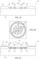
- the dielectric layer 103 is selectively etched inside the window 105 to form first trenches 105 and second trenches 106 ( Figures 19 and 20 ), which will then serve for the formation of anchors.
- the first trenches 105 extend continuously along respective closed paths nested one inside the other. In the embodiment described herein, in particular two circular and concentric first trenches 105 are opened.
- the second trenches 106 are enclosed inside the first trenches 105 and, in one embodiment, are organized in arrays which extend on closed paths L1', ..., LN' (three in the illustrated example) nested one in the other.
- the closed paths are concentric circumferences and each second trench 106 extends on a portion of a respective closed path L1', ..., LN'.
- Second trenches 106 which extend along a same closed path are separated from each other by portions of the dielectric layer 103.
- a first region 103a and a second region 103b of the dielectric layer 103 are connected to each other through the portions of the dielectric layer 103 which separate consecutive second trenches 106.
- a stop layer 107 for example alumina, and a connection and anchoring layer 108 are deposited on the microstructure wafer 101 ( Figures 21 and 22 ).
- the stop layer 107 coats the walls of the first trenches 105 and the second trenches 106, leaving a space therewithin which is filled by the connection and anchoring layer 108.
- Annular anchors 110 in the first trenches 105 and anchoring pins 111 in the second trenches 106 are thus formed.
- the anchoring pins 111 extend from the anchoring pad 113 to the substrate 102 perpendicular to the face 3c and along respective arcs of circumference parallel to the face 3c.
- the stop layer 107 and the connection layer are etched to open windows 112 on the second region 103b of the dielectric layer 103, in this case a plurality of windows 112 distributed along a circumference between the innermost first trench 105 and the outermost array of second trenches 106 ( Figure 22 ).
- connection and anchoring layer 8 radially internal to the windows 112 forms an anchoring pad 113 bonded to the anchoring pin 111.
- anchoring pad 113 forms an anchoring structure 115 with the anchoring pins 111.
- the anchoring pad 113 is depressed with respect to a face of the dielectric layer 103 opposite to the substrate 102.
- connection and anchoring layer 108 is also patterned to form anchoring pads 116 and conductive lines 117 according to the design preferences for the microelectromechanical devices to be formed in the microstructure wafer 101.
- a sacrificial layer 118 of silicon oxide is then deposited on the microstructure wafer 101 ( Figure 23 ), which is in contact with the dielectric layer 103 through the windows 112 and is selectively removed to form anchoring openings 120 over respective anchoring pads 116. Furthermore, one of the anchoring openings 120 exposes the anchoring pad 113 of the anchoring structure 115.
- a structural layer 121 of polycrystalline silicon is formed on the microstructure wafer 101 in contact with the anchoring pads 113, 116 through the anchoring openings 120, by growth in an epitaxial reactor.
- the structural layer 121 is then patterned to form fixed and movable parts of a gyroscope 122 in the first region 101a of the microstructure wafer 101 and an accelerometer (not shown) in the second region 101b.
- a fixed or stator portion 122a of the gyroscope 122 is anchored to the anchoring pad 113 of the anchoring structure 115 and is separated from the remaining part of the gyroscope 122 by gaps 122b which reach the portion of the sacrificial layer 118 which is connected to the second region 103a of the dielectric layer 103 through the windows 112.
- the sacrificial layer 118 is then removed where accessible to release the microstructures of the gyroscope 122 and the accelerometer, as shown in Figure 24 .
- the part of the dielectric layer 103 internal to the annular anchors 110 is also removed through the window 112.
- a cavity 125 is thus defined radially inside the annular anchors 110.
- a first portion 125a of the cavity 125, radially internal to the anchoring pins 111 communicates fluidically with a second portion 125b of the cavity 125, radially comprised between the annular anchors 110 and the anchoring pins 111, through passages 126 between adjacent anchoring pins 111 and channels 127 between concentric arrays of anchoring pins 111, as better illustrated in Figure 25 .
- the second portion 125b of the cavity 125 is fluidically coupled to the environment which surrounds the gyroscope 122 through the window 112 and the gaps around the fixed portion 122a.
- a cap wafer 130 is bonded to the microstructure wafer 101 using an adhesion layer 128 to seal the gyroscope 122 and the accelerometer (here indicated by 123) respectively inside a first chamber 32 and a second chamber 33, both at a first pressure P 1 '.
- the substrate 102 of the microstructure wafer 1 is then etched from the back in an anisotropic manner to form a channel 135 aligned with the first portion 125a of the cavity 125 ( Figure 27 ), thus forming a fluidic path that put the first chamber 132, where the gyroscope 122 is arranged, in communication with the outside through the window 112, the second portion 125b of the cavity 125, the passages 126 and the channels 127 between the anchoring pins 111, the first portion 125a of the cavity 125 and the channel 135.
- the etching of the semiconductor material ends on the stop layer 107, which protects the structural layer 121, in particular the fixed portion 122a of the gyroscope 122.
- the composite wafer 131 is then placed in an environment at a second pressure P 2 ', lower than the first pressure P 1 ', and is sealed ( Figures 28 and 29 ). More precisely, a sealing layer 137 is formed on the back of the substrate 102 by PVD or PECVD deposition and penetrates inside the channel 135 and the first region 125a of the cavity 125. The passages 126 between the anchoring pins 111 close for the deposit of the sealing layer 137 and the first portion 125a is fluidically insulated from the rest of the cavity 125 and the first chamber 132. The first chamber 132 is therefore sealed at the second pressure P 2 ', which may be accurately set and maintained.
- the composite wafer 131 is finally diced and divided into dice, each of which comprises an integrated microelectromechanical device 150 of the type illustrated in Figure 30 , where it is shown incorporated into a package 151.
- the process described advantageously allows two different microelectromechanical devices to be sealed in respective chambers at respective accurately controlled pressures, without using getter.
- the absence of getter, in particular, is advantageous for several reasons. Firstly, space in one of the chambers is clearly saved. This is highly desirable, given the ever-increasing trend towards miniaturization of devices. Secondly, the risk of early getter activation, which might alter the pressure in one or both chambers unpredictably, is completely eliminated. As it has been seen, in fact, the early activation during the steps in which the cap wafer is bonded to the microstructure wafer may cause both the absorption of gas from the high-pressure chamber by cross-talk and the saturation of the getter and therefore a higher-than-expected pressure in the low-pressure chamber. In turn, pressure variations in the chambers may affect the performance of microelectromechanical devices in an uncontrolled manner and, in any case, the actual operating conditions will be different from the preferred design conditions.
- the invention instead allows for very accurate control of the pressure in both chambers.
- the first chamber is in fact sealed exactly at the first pressure and no fluidic connection with the outside is established any longer.
- the first chamber is already definitively sealed when the second chamber is equalized at the second pressure and then sealed.
- Sealing the second chamber at lower pressure by using PVD or PECVD deposition is further advantageous because it allows the low pressure typically used for this type of processes to be exploited. This condition is particularly suitable for devices operating at very low pressure (in the order of microbars), such as geophones or bolometers.
- the process may be implemented mostly using processing steps in any case envisaged for the manufacturing of integrated microelectromechanical devices, simply by suitably designing the etching masks used. Dedicated steps are used in practice only for opening the channel from the back of the composite wafer, without therefore interfering with the processing steps on the front.
- the process according to the invention therefore does not entail significant increases in complexity and costs, in the face of a notable improvement in performance and a reduction in rejects.
- the cap wafer may be bonded to the microstructure wafer under low pressure conditions and, after putting one of the chambers (e.g. a chamber containing an accelerometer) in communication with the outside through a channel in the substrate and the anchor structures, seal under high pressure conditions.
- the chambers e.g. a chamber containing an accelerometer
- a plurality of fluidic paths between the outside and one of the two sealed chambers may be opened with the described techniques, in numbers and positions selected according to design preferences.
- the stop layer may be selectively removed before depositing the connection layer and left only in the position corresponding to the first portion of the cavity and the channel.
Landscapes
- Engineering & Computer Science (AREA)
- Microelectronics & Electronic Packaging (AREA)
- Manufacturing & Machinery (AREA)
- Computer Hardware Design (AREA)
- Micromachines (AREA)
Abstract
Description
- The present invention relates to a process for manufacturing microelectromechanical devices with chambers sealed at different pressures and a microelectromechanical device thereby manufactured.
- As is known, different microelectromechanical devices incorporated and sealed in a same package are used in many applications. For example, it is very common to integrate uniaxial or multiaxial gyroscopes and accelerometers into the same chip and therefore into the same package.
- A frequent issue is linked to the fact that the devices may have optimal operating conditions very different from each other, as in the case of gyroscopes and accelerometers. In fact, in order to reduce consumption due to air friction damping, it is preferable to have the gyroscopes work in an environment having low pressure, typically comprised between 0.1 mbar and 1 mbar. The gyroscopes are maintained constantly oscillating in resonance and low-pressure conditions allow the maintenance of the oscillations, reducing damping and dissipated energy. Accelerometers, on the other hand, normally operate under higher pressure conditions, for example between 1 mbar and a few atmospheres. Similar issues also arise with other types of devices operating under different conditions, for example resonators, wake-up systems, geophones or bolometers in combination with gyroscopes or accelerometers.
- A possible solution consists in including different devices in a same cavity or chamber of the package, wherein a pressure level corresponding to a trade-off between the preferred operating pressures is present. Solutions of this type are relatively simple to implement but may be unsatisfactory and affect performance.
- According to a different solution, the microelectromechanical devices are included in respective sealed and non-communicating chambers. In practice, the devices, for example gyroscopes and accelerometers, are manufactured in a first wafer, while, in a second wafer, caps are provided, and cavities are formed in positions corresponding to respective sensors. In the cavities intended for devices operating at lower pressure, a layer of an absorbent material or getter is also deposited. When the second wafer is bonded to the first wafer, for example by glass frit bonding or other wafer bonding technique, or at a later time with a dedicated step, the getter is thermally activated and absorbs the non-noble gases present in the chamber, reducing pressure. In this manner chambers sealed at different pressures may be obtained and all the devices may operate under preferred pressure conditions.
- However, even this solution is not free from limitations. Firstly, especially when particularly high pressures are desired in one of the chambers, the amount of available gaseous nitrogen may saturate the getter and, in this case, the pressure target in the chamber may not be achieved. On the other hand, to include an amount of getter sufficient to prevent saturation, the dimensions (base area and/or height) of the chamber may be greater than what would be sufficient for the sole microelectromechanical devices.
- Furthermore, during manufacturing the getter may be activated prematurely during the wafer bonding steps, before the chambers are completely sealed. In this case, the getter may also absorb gas from the higher-pressure chamber (cross-talk), creating a double drawback. On the one hand, in fact, the pressure of the getter-free chamber decreases and in any case the final pressure value is not accurately predictable. On the other hand, the getter may more easily saturate and therefore even in the low-pressure chamber the atmosphere may not reach the desired level.
-
US 2014/117472 A1 discloses a microelectromechanical device and a process for manufacturing microelectromechanical devices. The microelectromechanical device disclosed inUS 2014/117472 A1 comprises a substrate of semiconductor material; a dielectric layer on the substrate; a structural layer of semiconductor material on the dielectric layer; in the structural layer, a first microelectromechanical device and a second microelectromechanical device sealed respectively in a first chamber at a first pressure and in a second chamber at a second pressure, different from the first pressure; a channel traversing the substrate; in the dielectric layer, a first cavity fluidically coupled to the channel, a second cavity fluidically coupled to the first chamber and a fluidic passage between the first cavity and the second cavity; and a sealing layer that closes the fluidic passage and fluidically isolates the first cavity from the second cavity. - According to the process for manufacturing microelectromechanical devices disclosed in
US 2014/117472 A1 , a dielectric layer and a structural layer are formed on a first semiconductor wafer having a substrate of semiconductor material, the substrate being selectively etchable with respect to the stop layer. A first microelectromechanical device and a second microelectromechanical device are formed in the structural layer and are sealed respectively in a first chamber and a second chamber at a first pressure. The first chamber is fluidically coupled to an external environment through the substrate and is sealed at a second pressure different from the first pressure. In order to fluidically couple the first chamber to the external environment, a cavity fluidically coupled to the first chamber in the dielectric layer and a channel are formed. - Further examples of known microelectromechanical devices and processes to manufacture microelectromechanical devices are disclosed in
US 2015/123217 A1 andUS 2014/306300 A1 . - It is therefore an aim of the present invention to provide a microelectromechanical accelerometer that allows the limitations described to be overcome or at least mitigated.
- According to the present invention, a process for manufacturing microelectromechanical devices and a microelectromechanical device as defined in
claims - For a better understanding of the present invention, preferred embodiments are provided, by way of non-limiting example, with reference to the attached drawings, wherein:
-
Figure 1 is a section through a semiconductor wafer in an initial processing step of a process for manufacturing microelectromechanical devices in accordance with an embodiment of the present invention; -
Figure 2 shows an enlarged detail of the section ofFigure 1 in a subsequent processing step of the present process; -
Figure 3 is a top-plan view of a further enlarged detail of the wafer ofFigure 2 ; -
Figure 4 is a top-plan view of a detail of a semiconductor wafer in an intermediate processing step of a microelectromechanical process in accordance with a variant of the present invention; -
Figures 5 and 6 show the detail ofFigure 2 , in subsequent processing steps; -
Figures 7-9 show the section ofFigure 1 in subsequent processing steps; -
Figure 10 shows the view ofFigure 3 in a subsequent processing step; -
Figures 11-14 show the section ofFigure 1 in subsequent processing steps; -
Figure 15 shows the view ofFigure 3 in a subsequent processing step; -
Figure 16 is a cross-section through a microelectromechanical device in accordance with an embodiment of the present invention, obtained with the process illustrated inFigures 1-15 ; -
Figures 17 and 18 show a section through a semiconductor wafer in initial processing steps of a process for manufacturing microelectromechanical devices in accordance with a different embodiment of the present invention; -
Figure 19 shows an enlarged detail of the section ofFigure 17 in a subsequent processing step of the present process; -
Figure 20 is a top-plan view of a further enlarged detail of the wafer ofFigure 2 ; -
Figure 21 shows the detail ofFigure 19 , in subsequent processing steps; -
Figure 22 shows the view ofFigure 20 in a subsequent processing step; -
Figures 23-24 show the detail ofFigure 19 in subsequent processing steps; -
Figure 25 shows the view ofFigure 20 in a subsequent processing step; -
Figures 26-28 show the section ofFigure 17 in subsequent processing steps; -
Figure 29 shows the view ofFigure 20 in a subsequent processing step; -
Figure 30 is a cross-section through a microelectromechanical device in accordance with a different embodiment of the present invention, obtained with the process illustrated inFigures 17-29 . - With reference to
Figure 1 , asemiconductor wafer 1 comprises asubstrate 2, for example of monocrystalline silicon. Thewafer 1 is intended to accommodate microstructures of microelectromechanical devices and hereinafter it will be referred to asmicrostructure wafer 1. More in detail, a first region of themicrostructure wafer 1, indicated by 1a, is intended to accommodate a first microelectromechanical sensor operating at a first pressure, for example a gyroscope, and a second region of themicrostructure wafer 1, indicated by 1b, is intended to accommodate a second microelectromechanical sensor operating at a second pressure, higher than the first pressure, for example an accelerometer. However, it is understood that other microelectromechanical devices that require different operating pressures, such as resonators and wake-up systems, may be integrated into thesubstrate 2. - Initially, a
dielectric layer 3 of silicon oxide is deposited on thesubstrate 2 and is selectively etched in thefirst region 1a to formfirst trenches 5 andsecond trenches 6, which will then serve for the formation of anchors. Thefirst trenches 5 extend continuously along respective closed paths nested one inside the other. In the embodiment described herein, in particular two circular and concentricfirst trenches 5 are opened. - The
second trenches 6 are enclosed inside thefirst trenches 5 and, in one embodiment, are organized in arrays which extend on closed paths L1, ..., LN (three in the illustrated example) nested one in the other. In particular, in one embodiment the closed paths are concentric circumferences and eachsecond trench 6 extends on a portion of a respective closed path L1, ..., LN.Second trenches 6 which extend along a same closed path are separated from each other by portions of thedielectric layer 3. In this manner, afirst region 3a and asecond region 3b of thedielectric layer 3, respectively internal to thesecond trenches 6 and comprised between thefirst trenches 5 and thesecond trenches 6, are connected to each other through the portions of thedielectric layer 3 which separate consecutivesecond trenches 6. It is understood, however, that second trenches might not be organized in closed paths and might otherwise be arranged to form anchors, according to design preferences. For example, in the embodiment ofFigure 4 the second trenches, here indicated by 6', are aligned in rows. - The
microstructure wafer 1 is then covered with a stop layer 7 (Figure 5 ), thin enough to coat the inside of thefirst trenches 5 and thesecond trenches 6 without filling them. Thestop layer 7 is of a material with respect to which the silicon (or, in general, the material forming the substrate 2) is selectively etchable, for example alumina. - After the
stop layer 7, a connection andanchoring layer 8, for example of polycrystalline silicon, is deposited on themicrostructure wafer 1 and fills thefirst trenches 5 and thesecond trenches 6 forming anchoring rings 10 and anchoringpins 11 respectively, in this case with portions of thestop layer 7 which coat the inside of thefirst trenches 5 and thesecond trenches 6. The anchoring pins 11, in particular, are organized in concentric arrays, corresponding to respective closed paths L1, ..., LN. In each array, adjacent anchoring pins 11 are separated by portions of thedielectric layer 3. The dimensions of thesecond trenches 6 and the distances between consecutivesecond trenches 6 at least of the innermost array are selected so that the spaces between consecutive anchoring pins 11 may be sealed by a plasma deposition process, as detailed below. For example, the spacing between consecutive anchoring pins 11 may be between 1 µm and 5 µm. - Then (
Figure 6 ), thestop layer 7 and the connection andanchoring layer 8 are defined to open one ormore windows 12 between thefirst region 3a of thedielectric layer 3 and the innermost of the anchoring rings 10 (which corresponds to the innermost of the first trenches 5), so as to expose part of thedielectric layer 3. In the embodiment ofFigure 6 , in particular, asingle window 12 having annular shape is opened on thesecond region 3b of thedielectric layer 3. Consequently, a crown portion of thedielectric layer 3, of a shape corresponding to thewindow 12, is exposed. Alternatively, a plurality of windows may be opened, for example circular and distributed along a circumference. - In a zone radially internal to the
window 12, or more precisely over thefirst portion 3a of thedielectric layer 3 and over the anchoring pins 11 up to an inner edge of thewindow 12, remaining portions of the connection andanchoring layer 8 form ananchoring pad 13 bonded to the anchoring pins 11. In turn, theanchoring pad 13 forms an anchoringstructure 15 with the anchoring pins 11. In practice, theanchoring pad 13 extends on aface 3c of thedielectric layer 3 opposite to thesubstrate 2; the anchoring pins 11 extend from theanchoring pad 13 to thesubstrate 2 perpendicular to theface 3c and along respective arcs of circumference parallel to theface 3c. - In this step, the connection and
anchoring layer 8 is also shaped to form anchoringpads 16 andconductive lines 17 according to the design preferences for the microelectromechanical devices to be formed in themicrostructure wafer 1. - A
sacrificial layer 18 of silicon oxide is then deposited on the microstructure wafer 1 (Figure 7 ), which is in contact with thedielectric layer 3 through thewindow 12. Thesacrificial layer 18 is selectively removed to form anchoringopenings 20 overrespective anchoring pads 16. Furthermore, one of the anchoringopenings 20 exposes theanchoring pad 13 of the anchoringstructure 15. - Starting from a seed layer (not shown), a
structural layer 21 of polycrystalline silicon is formed on the microstructure wafer 1 (Figure 8 ) by growth in an epitaxial reactor. Thestructural layer 21 contacts theanchoring pads openings 20. Thestructural layer 21 is then defined by an anisotropic trench etching to form fixed and movable parts of agyroscope 22 in thefirst region 1a of themicrostructure wafer 1 and anaccelerometer 23 in thesecond region 1b. In particular, a fixed orstator portion 22a of thegyroscope 22 is anchored to theanchoring pad 13 of the anchoringstructure 15 and is separated from the remaining part of thegyroscope 22 bygaps 22b. However, it is understood that thestator portion 22a of thegyroscope 22 may extend beyond the anchoringstructure 15 and be in part anchored to thedielectric layer 3. Furthermore, thegaps 22b reach the portion of thesacrificial layer 18 which is connected to thesecond region 3a of thedielectric layer 3 through thewindows 12. - The
sacrificial layer 18 is then removed where accessible to free the microstructures of thegyroscope 22 and theaccelerometer 23, for example by etching in a hydrofluoric acid bath, as shown inFigure 9 . Furthermore, also the part of thedielectric layer 3 internal to theannular anchors 10, which is accessible through thewindow 12, is removed at the same time. The annular anchors 11, in this step, stop the removal of thedielectric layer 3. When the removal of thesacrificial layer 18 and thedielectric layer 3 is completed, a cavity 25 is defined radially inside theannular anchors 10 between the substrate and thestop layer 7. In particular, afirst portion 25a of the cavity 25, radially internal to the anchoring pins 11, communicates fluidically with asecond portion 25b of the cavity 25, radially comprised between theannular anchors 10 and the anchoring pins 11. The fluidic connection is obtained throughpassages 26 between adjacent anchoring pins 11 andchannels 27 between concentric arrays of anchoringpins 11, as better illustrated inFigure 10 . In turn, after thesacrificial layer 18 has been removed thesecond portion 25b of the cavity 25 is fluidically coupled to the environment which surrounds thegyroscope 22 through thewindow 12 and thegaps 22b around thestator portion 22a. - An adhesion layer 28 (
Figure 11 ) is then deposited on portions of thestructural layer 21 along closed paths which surround thegyroscope 22 and theaccelerometer 23. Theadhesion layer 28 may be of any suitable sealing material and used in semiconductor manufacturing processes for wafer bonding, for example and not limited to glass frit, an Al-Ge eutectic alloy, Au-Sn, Au-In, Au-Si, Si-Si, Si-SiO2 alloys. - Then (
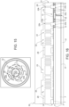
Figure 12 ), a cap wafer 30, preliminarily processed on an inner face according to the design preferences, is bonded to themicrostructure wafer 1 in a controlled atmosphere at a first pressure P1, forming a composite wafer 31. By adhering to theadhesion layer 28, the cap wafer 30 seals thegyroscope 22 and theaccelerometer 23 respectively inside afirst chamber 32 and asecond chamber 33, both at the first pressure P1. In one embodiment, the first pressure P1 is a design operating pressure of theaccelerometer 23, for example between 1 mbar and 5 bar. - As shown in
Figure 13 , thesubstrate 2 of themicrostructure wafer 1 is then anisotropically etched through a back side 2a to form achannel 35 aligned with thefirst portion 25a of the cavity 25. In this step, the etching of the semiconductor material ends on thestop layer 7, which protects thestructural layer 21, in particular the fixed orstator portion 22a of thegyroscope 22. In practice, therefore, a fluidic path is defined which puts thefirst chamber 32, where thegyroscope 22 is arranged, in communication with the outside through thewindow 12, thesecond portion 25b of the cavity 25, thepassages 26 and thechannels 27 between the anchoring pins 11, thefirst portion 25a of the cavity 25 and thechannel 35. - The composite wafer 31 is then placed in an environment at a second pressure P2, different from the first pressure P1 and lower in an embodiment, and is sealed (
Figures 14 and15 ). More precisely, asealing layer 37 is formed on the back side 2a of thesubstrate 2, for example by PVD (Physical Vapor Deposition) or PECVD (Plasma-Enhanced Chemical Vapor Deposition) deposition, and penetrates inside thechannel 35 and thefirst region 25a of the cavity 25. Due to the initial spacing between the second trenches 6 (and therefore between the adjacent anchoring pins 11 of the same array), thepassages 26 between the anchoring pins 11 close for the deposition of thesealing layer 37 and thefirst portion 25a is fluidically insulated from the rest of the cavity 25 and from thefirst chamber 32. Thefirst chamber 32 is therefore sealed at the second pressure P2, which may be accurately set and maintained. - After final processing steps which may comprise thinning, grinding, definition of contacts and cleaning, the composite wafer 31 is finally diced and divided into dice, each of which comprises a
microelectromechanical device 50 of the type illustrated inFigure 16 , where it is shown incorporated into apackage 51. - A different embodiment of the present invention will be described below with reference to
Figures 17-30 . Amicrostructure wafer 101 comprising asubstrate 102 of semiconductor material, for example monocrystalline silicon, is intended to accommodate microstructures of microelectromechanical devices. In particular, a first region of themicrostructure wafer 101, indicated by 101a, is intended to accommodate a first microelectromechanical sensor operating at a first pressure, for example a gyroscope, and a second region of themicrostructure wafer 101, indicated by 101b, is intended to accommodate a second microelectromechanical sensor operating at a second pressure, higher than the first pressure, for example an accelerometer. - Initially, a
dielectric layer 103, for example silicon oxide, is formed on thesubstrate 102 and selectively etched to open awindow 104, for example circular, which exposes a portion of thesubstrate 102 in thefirst region 101a of the microstructure wafer. - Then (
Figure 18 ), thedielectric layer 103 is increased by, for example, 0.5 µm or less by thermal oxidation or deposition of further silicon oxide and covers thesubstrate 102. - The
dielectric layer 103 is selectively etched inside thewindow 105 to formfirst trenches 105 and second trenches 106 (Figures 19 and 20 ), which will then serve for the formation of anchors. Thefirst trenches 105 extend continuously along respective closed paths nested one inside the other. In the embodiment described herein, in particular two circular and concentricfirst trenches 105 are opened. - The
second trenches 106 are enclosed inside thefirst trenches 105 and, in one embodiment, are organized in arrays which extend on closed paths L1', ..., LN' (three in the illustrated example) nested one in the other. In particular, in one embodiment the closed paths are concentric circumferences and eachsecond trench 106 extends on a portion of a respective closed path L1', ..., LN'.Second trenches 106 which extend along a same closed path are separated from each other by portions of thedielectric layer 103. In this manner, afirst region 103a and asecond region 103b of thedielectric layer 103, respectively internal to thesecond trenches 106 and comprised between thefirst trenches 105 and thesecond trenches 106, are connected to each other through the portions of thedielectric layer 103 which separate consecutivesecond trenches 106. - The process then proceeds substantially as already described and will be briefly recalled.
- A
stop layer 107, for example alumina, and a connection andanchoring layer 108 are deposited on the microstructure wafer 101 (Figures 21 and22 ). Thestop layer 107 coats the walls of thefirst trenches 105 and thesecond trenches 106, leaving a space therewithin which is filled by the connection andanchoring layer 108. Annular anchors 110 in thefirst trenches 105 and anchoringpins 111 in thesecond trenches 106 are thus formed. The anchoring pins 111 extend from theanchoring pad 113 to thesubstrate 102 perpendicular to theface 3c and along respective arcs of circumference parallel to theface 3c. - The
stop layer 107 and the connection layer are etched to openwindows 112 on thesecond region 103b of thedielectric layer 103, in this case a plurality ofwindows 112 distributed along a circumference between the innermostfirst trench 105 and the outermost array of second trenches 106 (Figure 22 ). - A portion of the connection and
anchoring layer 8 radially internal to thewindows 112 forms ananchoring pad 113 bonded to theanchoring pin 111. In turn, theanchoring pad 113 forms an anchoringstructure 115 with the anchoring pins 111. In practice, theanchoring pad 113 is depressed with respect to a face of thedielectric layer 103 opposite to thesubstrate 102. - The connection and
anchoring layer 108 is also patterned to form anchoringpads 116 andconductive lines 117 according to the design preferences for the microelectromechanical devices to be formed in themicrostructure wafer 101. - A sacrificial layer 118 of silicon oxide is then deposited on the microstructure wafer 101 (
Figure 23 ), which is in contact with thedielectric layer 103 through thewindows 112 and is selectively removed to form anchoringopenings 120 overrespective anchoring pads 116. Furthermore, one of the anchoringopenings 120 exposes theanchoring pad 113 of the anchoringstructure 115. Astructural layer 121 of polycrystalline silicon is formed on themicrostructure wafer 101 in contact with theanchoring pads openings 120, by growth in an epitaxial reactor. Thestructural layer 121 is then patterned to form fixed and movable parts of agyroscope 122 in thefirst region 101a of themicrostructure wafer 101 and an accelerometer (not shown) in thesecond region 101b. In particular, a fixed orstator portion 122a of thegyroscope 122 is anchored to theanchoring pad 113 of the anchoringstructure 115 and is separated from the remaining part of thegyroscope 122 by gaps 122b which reach the portion of the sacrificial layer 118 which is connected to thesecond region 103a of thedielectric layer 103 through thewindows 112. - The sacrificial layer 118 is then removed where accessible to release the microstructures of the
gyroscope 122 and the accelerometer, as shown inFigure 24 . At the same time, the part of thedielectric layer 103 internal to theannular anchors 110 is also removed through thewindow 112. A cavity 125 is thus defined radially inside the annular anchors 110. Afirst portion 125a of the cavity 125, radially internal to the anchoring pins 111, communicates fluidically with asecond portion 125b of the cavity 125, radially comprised between theannular anchors 110 and the anchoring pins 111, throughpassages 126 between adjacent anchoring pins 111 andchannels 127 between concentric arrays of anchoringpins 111, as better illustrated inFigure 25 . Furthermore, thesecond portion 125b of the cavity 125 is fluidically coupled to the environment which surrounds thegyroscope 122 through thewindow 112 and the gaps around the fixedportion 122a. - With reference to
Figure 26 , a cap wafer 130 is bonded to themicrostructure wafer 101 using an adhesion layer 128 to seal thegyroscope 122 and the accelerometer (here indicated by 123) respectively inside afirst chamber 32 and asecond chamber 33, both at a first pressure P1'. - The
substrate 102 of themicrostructure wafer 1 is then etched from the back in an anisotropic manner to form achannel 135 aligned with thefirst portion 125a of the cavity 125 (Figure 27 ), thus forming a fluidic path that put thefirst chamber 132, where thegyroscope 122 is arranged, in communication with the outside through thewindow 112, thesecond portion 125b of the cavity 125, thepassages 126 and thechannels 127 between the anchoring pins 111, thefirst portion 125a of the cavity 125 and thechannel 135. In this step, the etching of the semiconductor material ends on thestop layer 107, which protects thestructural layer 121, in particular the fixedportion 122a of thegyroscope 122. - The composite wafer 131 is then placed in an environment at a second pressure P2', lower than the first pressure P1', and is sealed (
Figures 28 and 29 ). More precisely, asealing layer 137 is formed on the back of thesubstrate 102 by PVD or PECVD deposition and penetrates inside thechannel 135 and thefirst region 125a of the cavity 125. Thepassages 126 between the anchoring pins 111 close for the deposit of thesealing layer 137 and thefirst portion 125a is fluidically insulated from the rest of the cavity 125 and thefirst chamber 132. Thefirst chamber 132 is therefore sealed at the second pressure P2', which may be accurately set and maintained. - After final processing steps, the composite wafer 131 is finally diced and divided into dice, each of which comprises an integrated microelectromechanical device 150 of the type illustrated in
Figure 30 , where it is shown incorporated into apackage 151. - The process described advantageously allows two different microelectromechanical devices to be sealed in respective chambers at respective accurately controlled pressures, without using getter. The absence of getter, in particular, is advantageous for several reasons. Firstly, space in one of the chambers is clearly saved. This is highly desirable, given the ever-increasing trend towards miniaturization of devices. Secondly, the risk of early getter activation, which might alter the pressure in one or both chambers unpredictably, is completely eliminated. As it has been seen, in fact, the early activation during the steps in which the cap wafer is bonded to the microstructure wafer may cause both the absorption of gas from the high-pressure chamber by cross-talk and the saturation of the getter and therefore a higher-than-expected pressure in the low-pressure chamber. In turn, pressure variations in the chambers may affect the performance of microelectromechanical devices in an uncontrolled manner and, in any case, the actual operating conditions will be different from the preferred design conditions.
- The invention instead allows for very accurate control of the pressure in both chambers. The first chamber is in fact sealed exactly at the first pressure and no fluidic connection with the outside is established any longer. In particular, the first chamber is already definitively sealed when the second chamber is equalized at the second pressure and then sealed.
- Sealing the second chamber at lower pressure by using PVD or PECVD deposition is further advantageous because it allows the low pressure typically used for this type of processes to be exploited. This condition is particularly suitable for devices operating at very low pressure (in the order of microbars), such as geophones or bolometers.
- The process may be implemented mostly using processing steps in any case envisaged for the manufacturing of integrated microelectromechanical devices, simply by suitably designing the etching masks used. Dedicated steps are used in practice only for opening the channel from the back of the composite wafer, without therefore interfering with the processing steps on the front. The process according to the invention therefore does not entail significant increases in complexity and costs, in the face of a notable improvement in performance and a reduction in rejects.
- Furthermore, a dedicated etching is not necessary to remove residual portions of the stop layer.
- Finally, it is clear that modifications and variations may be made to the microelectromechanical accelerometer described, without departing from the scope of the present invention, as defined in the attached claims.
- For example, the cap wafer may be bonded to the microstructure wafer under low pressure conditions and, after putting one of the chambers (e.g. a chamber containing an accelerometer) in communication with the outside through a channel in the substrate and the anchor structures, seal under high pressure conditions.
- Furthermore, a plurality of fluidic paths between the outside and one of the two sealed chambers may be opened with the described techniques, in numbers and positions selected according to design preferences.
- According to further variants, the stop layer may be selectively removed before depositing the connection layer and left only in the position corresponding to the first portion of the cavity and the channel.
Claims (16)
- A process for manufacturing microelectromechanical devices comprising:on a first semiconductor wafer (1; 101) comprising a substrate (2; 102) of semiconductor material, forming a dielectric layer (3; 103), a structural layer (21; 121) and a stop layer (7; 107) between the dielectric layer (3; 103) and the structural layer (21; 121), the substrate (2; 102) being selectively etchable with respect to the stop layer (7; 107);forming a first microelectromechanical device (22; 122) and a second microelectromechanical device (23; 123) in the structural layer (21; 121);sealing the first microelectromechanical device (22; 122) and the second microelectromechanical device (23; 123) respectively in a first chamber (32; 132) and in a second chamber (33; 133) at a first pressure (P1; P1');fluidically coupling the first chamber (32; 132) to an external environment through the substrate (2; 102); andsealing the first chamber (32; 132) at a second pressure (P2; P2') different from the first pressure (P1; P1');wherein fluidically coupling comprises:forming a cavity (25; 125) fluidically coupled to the first chamber (32; 132) in the dielectric layer (3; 103) and extending from the substrate (2; 102) to a portion of the stop layer (7; 107);etching the substrate (2; 102) to form a channel (35; 135) through the substrate (2; 102) in a position corresponding to the cavity (25; 125) and the portion of the stop layer (7; 107); andending the etching of the substrate (2; 102) against the stop layer (7; 107).
- The process according to claim 1, comprising forming an anchoring structure (15; 115) extending through the cavity and configured to anchor a fixed portion (22a; 122a) of the first microelectromechanical device (22; 122) to the substrate.
- The process according to claim 2, wherein the anchoring structure (15; 115) delimits, in the cavity (25; 125), an inner first portion (25a; 125a) and an outer second portion (25b; 125b) and forms fluidic passages (26, 27; 126, 127) between the first portion (25a; 125a) and the second portion (25b; 125b) of the cavity (25; 125).
- The process according to claim 3, wherein forming the anchoring structure (15; 115) comprises:opening first trenches (5; 105) in the dielectric layer (3; 103) to the substrate (2; 102), the first trenches (5; 105) extending continuously along respective first closed paths nested one inside the other;opening second trenches (6; 106) in the dielectric layer (3; 103) to the substrate (2; 102), the second trenches (6; 106) being enclosed inside the first trenches (5; 105) and extending on portions of respective second closed paths nested one inside the other;wherein a first region (3a; 103a) of the dielectric layer (3; 103), internal to the second trenches (6; 106) and of a shape corresponding to the first portion (25a; 125a) of the cavity (25; 15), and a second region (3b; 103b) of the dielectric layer (3; 103), comprised between the first trenches (5; 105) and the second trenches (6; 106) and of a shape corresponding to the second portion (25b; 125b) of the cavity (25; 15), are connected to each other through portions of the dielectric layer (3; 103) separating second consecutive trenches (6; 106).
- The process according to claim 4, wherein forming the anchoring structure (15; 115) comprises forming a semiconductor connection and anchoring layer (8; 108) on the stop layer (7; 107), so as to fill the first trenches (5; 105) and the second trenches (6; 106) and respectively form annular first anchoring elements (10; 110) and second anchoring elements (11; 111);
patterning the connection and anchoring layer (8; 108) so as to define an anchoring pad (13; 113) bonded to the second anchoring elements (11; 111) over the first region (3a; 103a) of the dielectric layer (3; 103). - The process according to claim 5, comprising selectively removing the connection and anchoring layer (8; 108) and the stop layer (7; 107) so as to open at least one window (12; 112) on the second region (3b; 103b) of the dielectric layer (3; 103) around the anchoring structure (15; 115) and expose a portion of the dielectric layer (3; 103) of a shape corresponding to the window (12; 112).
- The process according to claim 6, comprising forming a dielectric sacrificial layer (18; 118) in contact with the second region (3b; 103b) of the dielectric layer (3; 103) through the at least one window (12; 112).
- The process according to claim 7, wherein the sacrificial layer (18; 118) is formed on the stop layer (7; 107) .
- The process according to claim 7 or 8, comprising:removing the sacrificial layer (18; 118) selectively over the anchoring pad (13; 113); andforming a semiconductor structural layer (21; 121) on the sacrificial layer and in contact with the anchoring pad (13; 113);wherein forming the first microelectromechanical device (22; 122) and the second microelectromechanical device (23; 123) comprises etching the structural layer (21; 121) in an anisotropic manner to the sacrificial layer (18; 118).
- The process according to claim 9, wherein forming the cavity (25; 125) comprises removing the sacrificial layer (18; 118) and removing the first region (3a; 103a) and the second region (3b; 103b) of the dielectric layer (3; 103) through the at least one window (12; 112).
- The process according to any of claims 3 to 10, wherein the channel (35; 135) is aligned with the first portion (25a; 125a) of the cavity (25; 125).
- The process according to claim 11, wherein sealing the first chamber (32; 132) at the second pressure (P2; P2') comprises depositing a sealing layer (37; 137) on a back side (2a; 102a) of the substrate (2; 102) and through the channel (35; 135).
- The process according to any of claims 3 to 12, wherein sealing the first chamber (32; 132) at the second pressure (P2; P2') comprises fluidically insulating the first portion (25a; 125a) from the rest of the cavity (25; 125) and from the first chamber (32; 132).
- The process according to any of claims 3 to 13, wherein sealing the first chamber (32; 132) at the second pressure (P2; P2') comprises closing the fluidic passages (26, 27; 126, 127) between the first portion (25a; 125a) and the second portion (25b; 125b) of the cavity (25; 125).
- The process according to any of the preceding claims, wherein sealing the first microelectromechanical device (22; 122) and the second microelectromechanical device (23; 123) comprises bonding a second semiconductor wafer (30; 130) to the first semiconductor wafer (1; 101).
- A microelectromechanical device comprising:a substrate (2; 102) of semiconductor material;a dielectric layer (3; 103) on the substrate (2; 102);a structural layer (21; 121) of semiconductor material on the dielectric layer (3; 103);a stop layer (7; 107) interposed between the dielectric layer (3; 103) and the structural layer (21; 121), the substrate (2; 102) being selectively etchable with respect to the stop layer (7; 107);in the structural layer (21; 121), a first microelectromechanical device (22; 122) and a second microelectromechanical device (23; 123) sealed respectively in a first chamber (32; 132) at a first pressure (P1; P1') and in a second chamber (33; 133) at a second pressure (P2; P2'), different from the first pressure (P1; P1');a channel (35; 135) traversing the substrate (2; 102);in the dielectric layer (3; 103) between the substrate (2; 102) and a portion of the stop layer (7; 107), a first cavity (25a; 125a) fluidically coupled to the channel (35), a second cavity (25b ; 125b) fluidically coupled to the first chamber (32; 132) and fluidic passages (26, 27; 126, 127) between the first cavity (25a; 125a) and the second cavity (25b; 125b); anda sealing layer (37; 137) which closes the fluidic passages (26, 27; 126, 127) and fluidically insulates the first cavity (25a; 125a) from the second cavity (25b; 125b).
Applications Claiming Priority (1)
| Application Number | Priority Date | Filing Date | Title |
|---|---|---|---|
| IT102023000026853A IT202300026853A1 (en) | 2023-12-15 | 2023-12-15 | PROCESS FOR MANUFACTURING MICROELECTROMECHANICAL DEVICES WITH CHAMBERS SEALED AT DIFFERENT PRESSURES AND THE MICROELECTROMECHANICAL DEVICE SO MANUFACTURED |
Publications (1)
| Publication Number | Publication Date |
|---|---|
| EP4574748A1 true EP4574748A1 (en) | 2025-06-25 |
Family
ID=90124176
Family Applications (1)
| Application Number | Title | Priority Date | Filing Date |
|---|---|---|---|
| EP24216750.0A Pending EP4574748A1 (en) | 2023-12-15 | 2024-12-02 | Process for manufacturing microelectromechanical devices with chambers sealed at different pressures and microelectromechanical device thereby manufactured |
Country Status (3)
| Country | Link |
|---|---|
| US (1) | US20250197199A1 (en) |
| EP (1) | EP4574748A1 (en) |
| IT (1) | IT202300026853A1 (en) |
Citations (3)
| Publication number | Priority date | Publication date | Assignee | Title |
|---|---|---|---|---|
| US20140117472A1 (en) | 2012-10-26 | 2014-05-01 | Robert Bosch Gmbh | Micromechanical component |
| US20140306300A1 (en) | 2011-11-03 | 2014-10-16 | Continental Teves Ag & Co. Ohg | Component and Method for Producing a Component |
| US20150123217A1 (en) | 2013-11-06 | 2015-05-07 | Robert Bosch Gmbh | Micromechanical sensor unit and method for manufacturing micromechanical sensor units |
-
2023
- 2023-12-15 IT IT102023000026853A patent/IT202300026853A1/en unknown
-
2024
- 2024-12-02 EP EP24216750.0A patent/EP4574748A1/en active Pending
- 2024-12-04 US US18/968,911 patent/US20250197199A1/en active Pending
Patent Citations (3)
| Publication number | Priority date | Publication date | Assignee | Title |
|---|---|---|---|---|
| US20140306300A1 (en) | 2011-11-03 | 2014-10-16 | Continental Teves Ag & Co. Ohg | Component and Method for Producing a Component |
| US20140117472A1 (en) | 2012-10-26 | 2014-05-01 | Robert Bosch Gmbh | Micromechanical component |
| US20150123217A1 (en) | 2013-11-06 | 2015-05-07 | Robert Bosch Gmbh | Micromechanical sensor unit and method for manufacturing micromechanical sensor units |
Also Published As
| Publication number | Publication date |
|---|---|
| US20250197199A1 (en) | 2025-06-19 |
| IT202300026853A1 (en) | 2025-06-15 |
Similar Documents
| Publication | Publication Date | Title |
|---|---|---|
| EP1716072B1 (en) | Integrated getter area for wafer level encapsulated microelectromechanical systems | |
| US8183474B2 (en) | Microcomponent provided with a cavity delimited by a cap with enhanced mechanical resistance | |
| US7514283B2 (en) | Method of fabricating electromechanical device having a controlled atmosphere | |
| US6479320B1 (en) | Vacuum package fabrication of microelectromechanical system devices with integrated circuit components | |
| US6521477B1 (en) | Vacuum package fabrication of integrated circuit components | |
| US5604160A (en) | Method for packaging semiconductor devices | |
| US7259436B2 (en) | Micromechanical component and corresponding production method | |
| JP4869943B2 (en) | Micropart with sealed microcavity and method for manufacturing such micropart | |
| CN101142137A (en) | Micromechanical element and method of manufacturing micromechanical element | |
| KR20030023613A (en) | Vacuum Package Fabrication of Microelectromechanical System Devices with Integrated Circuit Components | |
| WO2004022478A1 (en) | Soi polysilicon trench refill perimeter oxide anchor scheme | |
| EP2432727B1 (en) | Substrate with multiple encapsulated pressures | |
| US20250197199A1 (en) | Process for manufacturing microelectromechanical devices with chambers sealed at different pressures and microelectromechanical device thereby manufactured | |
| CN120157083A (en) | Process for manufacturing a micro-electromechanical device having a chamber and a micro-electromechanical device | |
| US20250197198A1 (en) | Manufacturing process for microelectromechanical devices having improved sealing performance | |
| EP2435357B1 (en) | Method of accurately spacing z-axis electrode | |
| JPH0797643B2 (en) | Method for manufacturing pressure transducer | |
| US12017909B2 (en) | Fabrication method for a MEMS device | |
| US20240124299A1 (en) | Process for manufacturing a micro-electro-mechanical device including two chambers at different pressures and related micro-electro-mechanical device | |
| US20250178889A1 (en) | Process for manufacturing a combined microelectromechanical device with a reduced cross-talk and corresponding combined microelectromechanical device | |
| EP2736071B1 (en) | Wafer level package with getter | |
| CN120157082A (en) | Fabrication process of micro-electromechanical devices with improved sealing performance | |
| Ayanoor-Vitikkate et al. | Wafer scale encapsulation of wide gaps using oxidation of sacrificial beams |
Legal Events
| Date | Code | Title | Description |
|---|---|---|---|
| PUAI | Public reference made under article 153(3) epc to a published international application that has entered the european phase |
Free format text: ORIGINAL CODE: 0009012 |
|
| STAA | Information on the status of an ep patent application or granted ep patent |
Free format text: STATUS: THE APPLICATION HAS BEEN PUBLISHED |
|
| AK | Designated contracting states |
Kind code of ref document: A1 Designated state(s): AL AT BE BG CH CY CZ DE DK EE ES FI FR GB GR HR HU IE IS IT LI LT LU LV MC ME MK MT NL NO PL PT RO RS SE SI SK SM TR |
|
| STAA | Information on the status of an ep patent application or granted ep patent |
Free format text: STATUS: REQUEST FOR EXAMINATION WAS MADE |
|
| 17P | Request for examination filed |
Effective date: 20251222 |
|
| GRAP | Despatch of communication of intention to grant a patent |
Free format text: ORIGINAL CODE: EPIDOSNIGR1 |
|
| STAA | Information on the status of an ep patent application or granted ep patent |
Free format text: STATUS: GRANT OF PATENT IS INTENDED |
|
| RIC1 | Information provided on ipc code assigned before grant |
Ipc: B81C 1/00 20060101AFI20260119BHEP Ipc: B81B 7/02 20060101ALI20260119BHEP |
|
| INTG | Intention to grant announced |
Effective date: 20260204 |