EP4574343A1 - Power tool - Google Patents
Power tool Download PDFInfo
- Publication number
- EP4574343A1 EP4574343A1 EP24208530.6A EP24208530A EP4574343A1 EP 4574343 A1 EP4574343 A1 EP 4574343A1 EP 24208530 A EP24208530 A EP 24208530A EP 4574343 A1 EP4574343 A1 EP 4574343A1
- Authority
- EP
- European Patent Office
- Prior art keywords
- pcb
- protective layer
- layer
- covered
- printed
- Prior art date
- Legal status (The legal status is an assumption and is not a legal conclusion. Google has not performed a legal analysis and makes no representation as to the accuracy of the status listed.)
- Pending
Links
Images



Classifications
-
- B—PERFORMING OPERATIONS; TRANSPORTING
- B25—HAND TOOLS; PORTABLE POWER-DRIVEN TOOLS; MANIPULATORS
- B25F—COMBINATION OR MULTI-PURPOSE TOOLS NOT OTHERWISE PROVIDED FOR; DETAILS OR COMPONENTS OF PORTABLE POWER-DRIVEN TOOLS NOT PARTICULARLY RELATED TO THE OPERATIONS PERFORMED AND NOT OTHERWISE PROVIDED FOR
- B25F5/00—Details or components of portable power-driven tools not particularly related to the operations performed and not otherwise provided for
- B25F5/02—Construction of casings, bodies or handles
-
- H—ELECTRICITY
- H05—ELECTRIC TECHNIQUES NOT OTHERWISE PROVIDED FOR
- H05K—PRINTED CIRCUITS; CASINGS OR CONSTRUCTIONAL DETAILS OF ELECTRIC APPARATUS; MANUFACTURE OF ASSEMBLAGES OF ELECTRICAL COMPONENTS
- H05K3/00—Apparatus or processes for manufacturing printed circuits
- H05K3/22—Secondary treatment of printed circuits
- H05K3/28—Applying non-metallic protective coatings
- H05K3/284—Applying non-metallic protective coatings for encapsulating mounted components
-
- H—ELECTRICITY
- H05—ELECTRIC TECHNIQUES NOT OTHERWISE PROVIDED FOR
- H05K—PRINTED CIRCUITS; CASINGS OR CONSTRUCTIONAL DETAILS OF ELECTRIC APPARATUS; MANUFACTURE OF ASSEMBLAGES OF ELECTRICAL COMPONENTS
- H05K3/00—Apparatus or processes for manufacturing printed circuits
- H05K3/22—Secondary treatment of printed circuits
- H05K3/28—Applying non-metallic protective coatings
-
- H—ELECTRICITY
- H01—ELECTRIC ELEMENTS
- H01M—PROCESSES OR MEANS, e.g. BATTERIES, FOR THE DIRECT CONVERSION OF CHEMICAL ENERGY INTO ELECTRICAL ENERGY
- H01M50/00—Constructional details or processes of manufacture of the non-active parts of electrochemical cells other than fuel cells, e.g. hybrid cells
- H01M50/20—Mountings; Secondary casings or frames; Racks, modules or packs; Suspension devices; Shock absorbers; Transport or carrying devices; Holders
- H01M50/247—Mountings; Secondary casings or frames; Racks, modules or packs; Suspension devices; Shock absorbers; Transport or carrying devices; Holders specially adapted for portable devices, e.g. mobile phones, computers, hand tools or pacemakers
-
- H—ELECTRICITY
- H01—ELECTRIC ELEMENTS
- H01M—PROCESSES OR MEANS, e.g. BATTERIES, FOR THE DIRECT CONVERSION OF CHEMICAL ENERGY INTO ELECTRICAL ENERGY
- H01M50/00—Constructional details or processes of manufacture of the non-active parts of electrochemical cells other than fuel cells, e.g. hybrid cells
- H01M50/20—Mountings; Secondary casings or frames; Racks, modules or packs; Suspension devices; Shock absorbers; Transport or carrying devices; Holders
- H01M50/284—Mountings; Secondary casings or frames; Racks, modules or packs; Suspension devices; Shock absorbers; Transport or carrying devices; Holders with incorporated circuit boards, e.g. printed circuit boards [PCB]
-
- H—ELECTRICITY
- H01—ELECTRIC ELEMENTS
- H01M—PROCESSES OR MEANS, e.g. BATTERIES, FOR THE DIRECT CONVERSION OF CHEMICAL ENERGY INTO ELECTRICAL ENERGY
- H01M50/00—Constructional details or processes of manufacture of the non-active parts of electrochemical cells other than fuel cells, e.g. hybrid cells
- H01M50/50—Current conducting connections for cells or batteries
- H01M50/502—Interconnectors for connecting terminals of adjacent batteries; Interconnectors for connecting cells outside a battery casing
- H01M50/519—Interconnectors for connecting terminals of adjacent batteries; Interconnectors for connecting cells outside a battery casing comprising printed circuit boards [PCB]
-
- H—ELECTRICITY
- H05—ELECTRIC TECHNIQUES NOT OTHERWISE PROVIDED FOR
- H05K—PRINTED CIRCUITS; CASINGS OR CONSTRUCTIONAL DETAILS OF ELECTRIC APPARATUS; MANUFACTURE OF ASSEMBLAGES OF ELECTRICAL COMPONENTS
- H05K1/00—Printed circuits
- H05K1/02—Details
- H05K1/11—Printed elements for providing electric connections to or between printed circuits
- H05K1/111—Pads for surface mounting, e.g. lay-out
-
- H—ELECTRICITY
- H05—ELECTRIC TECHNIQUES NOT OTHERWISE PROVIDED FOR
- H05K—PRINTED CIRCUITS; CASINGS OR CONSTRUCTIONAL DETAILS OF ELECTRIC APPARATUS; MANUFACTURE OF ASSEMBLAGES OF ELECTRICAL COMPONENTS
- H05K3/00—Apparatus or processes for manufacturing printed circuits
- H05K3/22—Secondary treatment of printed circuits
- H05K3/28—Applying non-metallic protective coatings
- H05K3/285—Permanent coating compositions
- H05K3/287—Photosensitive compositions
-
- H—ELECTRICITY
- H05—ELECTRIC TECHNIQUES NOT OTHERWISE PROVIDED FOR
- H05K—PRINTED CIRCUITS; CASINGS OR CONSTRUCTIONAL DETAILS OF ELECTRIC APPARATUS; MANUFACTURE OF ASSEMBLAGES OF ELECTRICAL COMPONENTS
- H05K5/00—Casings, cabinets or drawers for electric apparatus
- H05K5/02—Details
- H05K5/0217—Mechanical details of casings
Definitions
- the present application relates to an electrical control device and, in particular, to a power tool, a power device, and a battery pack.
- the printed circuit board is widely used in electrical control devices. After the PCB is manufactured, the surface of the PCB needs to be protected.
- the surface protection of the PCB of the current product adopts the manual hand brushing process with G6 silicone. This method is inefficient, lots of glue materials are wasted, and excess glue on the appearance inspection station needs to be removed, resulting in serious material waste and making it difficult to achieve automated operations.
- An object of the present application is to solve or at least alleviate part or all of the preceding problems. For this reason, the object of the present application is to provide a power tool, a power device, and a battery pack.
- the present invention adopts the technical solutions below.
- a power tool includes an electric motor, an output portion, a housing, and at least one PCB.
- the electric motor includes a drive shaft rotating about a drive axis.
- the output portion is driven by the electric motor to output power.
- the housing accommodates the electric motor.
- At least one PCB is electrically connected to the electric motor, where at least part of the at least one PCB is covered with a three-dimensional (3D) printed protective layer.
- the thickness of the 3D printed protective layer is greater than or equal to 20 ⁇ m and less than or equal to 2000 ⁇ m.
- At least two regions on a PCB of the at least one PCB are covered with the 3D printed protective layer with different thicknesses.
- a region on a PCB of the at least one PCB is covered with a 3D printed enclosure layer.
- a region enclosed by the enclosure layer is capable of being covered with a protective layer different from the 3D printed protective layer.
- the 3D printed protective layer is formed by spraying a PCB of the at least one PCB multiple times.
- the thickness of a single-layer spray coating is greater than or equal to 20 ⁇ m.
- a power device includes a mounting housing, a first connection terminal, a second connection terminal, and at least one PCB.
- the mounting housing has a mounting cavity.
- the first connection terminal is disposed in the mounting housing and electrically connected to an external power supply.
- the second connection terminal is disposed in the mounting housing and used for outputting electrical energy.
- At least one PCB is electrically connected to both the first connection terminal and the second connection terminal, where at least part of the at least one PCB is covered with a 3D printed protective layer.
- At least two regions on a PCB of the at least one PCB are covered with the 3D printed protective layer with different thicknesses.
- a region on a PCB of the at least one PCB is covered with a 3D printed enclosure layer.
- a region enclosed by the enclosure layer is capable of being covered with a protective layer different from the 3D printed protective layer.
- the 3D printed protective layer is formed by spraying a PCB of the at least one PCB multiple times.
- the thickness of a single-layer spray coating is greater than or equal to 20 ⁇ m.
- a battery pack includes a housing, a cell, and at least one PCB.
- the housing has an accommodation cavity.
- the cell is disposed in the accommodation cavity.
- At least one PCB is electrically connected to the cell, where at least part of the at least one PCB is covered with a 3D printed protective layer.
- At least two regions on a PCB of the at least one PCB are covered with the 3D printed protective layer with different thicknesses.
- a region on a PCB of the at least one PCB is covered with a 3D printed enclosure layer.
- a region enclosed by the enclosure layer is capable of being covered with a protective layer different from the 3D printed protective layer.
- the 3D printed protective layer is formed by spraying a PCB of the at least one PCB multiple times.
- the thickness of a single-layer spray coating is less than or equal to 30 ⁇ m.
- the present application has the beneficial effects below.
- the power tool, the power device, and the battery pack provided in the present application each use the PCB as a control unit.
- the PCB is covered with the 3D printed protective layer
- the automated device is used to accurately coat regions to be protected on the PCB, and 3D printed protective layers may be stacked layer by layer so that the manual glue brushing process is replaced, thereby greatly improving the efficiency and reducing material waste.
- the term "and/or” is a kind of association relationship describing the relationship between associated objects, which means that there can be three kinds of relationships.
- a and/or B can indicate that A exists alone, A and B exist simultaneously, and B exists alone.
- the character "/" in this application generally indicates that the contextual associated objects belong to an "and/or” relationship.
- connection may be direct connection, combination, coupling or installation, and may also be indirect connection, combination, coupling or installation.
- direct connection means that two members or assemblies are connected together without intermediaries
- indirect connection means that two members or assemblies are respectively connected with at least one intermediate members and the two members or assemblies are connected by the at least one intermediate members.
- connection and “coupling” are not limited to physical or mechanical connections or couplings, and may include electrical connections or couplings.
- a relative term (such as “about”, “approximately”, and “substantially) used in conjunction with quantity or condition includes a stated value and has a meaning dictated by the context.
- the relative term includes at least a degree of error associated with the measurement of a particular value, a tolerance caused by manufacturing, assembly, and use associated with the particular value, and the like.
- Such relative term should also be considered as disclosing the range defined by the absolute values of the two endpoints.
- the relative term may refer to plus or minus of a certain percentage (such as 1%, 5%, 10%, or more) of an indicated value. A value that did not use the relative term should also be disclosed as a particular value with a tolerance.
- “substantially” when expressing a relative angular position relationship may refer to adding or subtracting a certain degree (such as 1 degree, 5 degrees, 10 degrees or more) to the indicated angle.
- a function performed by an assembly may be performed by one assembly, multiple assemblies, one member, or multiple members.
- a function performed by a member may be performed by one member, an assembly, or a combination of members.
- controller In this application, the terms “controller”, “processor”, “central processor”, “CPU” and “MCU” are interchangeable. Where a unit “controller”, “processor”, “central processing”, “CPU”, or “MCU” is used to perform a specific function, the specific function may be implemented by a single aforementioned unit or a plurality of the aforementioned unit.
- the term "device”, “module” or “unit” may be implemented in the form of hardware or software to achieve specific functions.
- the terms “computing”, “judging”, “controlling”, “determining”, “recognizing” and the like refer to the operations and processes of a computer system or similar electronic computing device (e.g., controller, processor, etc.).
- the present invention provides a power tool.
- the power tool 100 is an electric drill.
- the present application is not limited to the disclosed examples but may be applied to other types of power tools 100, for example, a hedge trimmer, or a sander.
- the power tool 100 may be a table tool, for example, a table saw or a miter saw.
- the power tool 100 may be a push power tool, for example, a push mower or a push snow thrower.
- the power tool 100 may be a riding power tool, for example, a riding mower, a riding vehicle, or an all-terrain vehicle.
- the power tool 100 may be a robotic tool, for example, a robotic mower or a robotic snow thrower.
- the power tool 100 may be an electric drill, an electric vehicle, or the like.
- the power tool 100 may be a garden tool, for example, a hedge trimmer, a blower, a mower, or a chainsaw.
- the power tool 100 may be a decorating tool, for example, a screwdriver, a nail gun, a circular saw, or a sander.
- the power tool 100 may be a vegetation care tool, for example, a string trimmer, a mower, a hedge trimmer, or a chainsaw.
- the power tool 100 may be a cleaning tool, for example, a blower, a snow thrower, or a cleaning machine.
- the power tool 100 may be a drilling tool, for example, a drill, a screwdriver, a wrench, or an electric hammer.
- the power tool 100 may be a sawing tool, for example, a reciprocating saw, a jigsaw, or a circular saw.
- the power tool 100 may be a table tool, for example, a table saw, a miter saw, a metal cutter, or an electric router.
- the power tool 100 may be a sanding tool, for example, an angle grinder or a sander.
- the power tool 100 may be another tool, for example, a machine tool or a fan.
- the power tool 100 includes an electric motor 12, an output portion 11, a housing 10, and at least one PCB 4.
- the electric motor 12 includes a drive shaft 121 rotating about a drive axis 101.
- the output portion 11 is driven by the electric motor 12 to output power.
- the housing 10 is used for accommodating the electric motor 12.
- At least one PCB 4 is electrically connected to the electric motor 12.
- the PCB may be a control board of the electric motor 12 or a control board of other additional functions in the power tool 100, for example, an illumination circuit board or a switch circuit board light.
- the case where the PCB is the control board of the electric motor 12 is used as an example for description.
- Various electronic components of the electric motor 12 control circuit may be electrically coupled to the PCB so that at least the start and stop, forward and reverse rotation, and the rotational speed of the electric motor 12 can be controlled, thereby driving the output portion 11 to output a driving force to drive the tool accessory to work, for example, to drive the drill bit to drill holes.
- the PCB 4 is used as the control center of the power tool 100, and many electronic components are disposed on the PCB 4. Therefore, during the manufacturing process, the surface of the PCB 4 needs to be protected.
- the surface protection of the PCB 4 of the current product adopts the manual hand brushing process with G6 silicone. This method is inefficient, lots of glue materials are wasted, and excess glue on the appearance inspection station needs to be removed, making the process more complicated.
- the automated device is used to adopt 3D printing technologies to accurately coat regions to be protected on the PCB 4, and 3D printed protective layers42 may be stacked layer by layer so that the manual glue brushing process is replaced, thereby greatly improving the efficiency and reducing material waste.
- an image or graphic of the to-be-sprayed region of the PCB to be sprayed with a protective layer may be preset in the 3D printing automated device. After the PCB is placed at a preset position, the automated device can spray the to-be-protected region with the protective material in response to a printing operation. In this example, the spraying accuracy of the automated device when the 3D printing of the protective layer is performed can reach 0.3 mm or higher.
- the present application does not provide any further explanation on the automated device for implementing automated 3D printing technologies.
- a 3D printed protective layer 42 may be applied to at least one PCB in the power tool 100.
- the PCB to which the 3D printed protective layer 42 needs to be applied may be selected according to the complexity of the component arrangement or the number of components on the PCB.
- the thickness of the 3D printed protective layer 42 is greater than or equal to 20 ⁇ m and less than or equal to 2000 ⁇ m, or greater than or equal to 30 ⁇ m and less than or equal to 1000 ⁇ m, or greater than or equal to 20 ⁇ m and less than or equal to 500 ⁇ m, or greater than or equal to 20 ⁇ m, for example, 30 ⁇ m, 31 ⁇ m, 32 ⁇ m, 35 ⁇ m, ..., 50 ⁇ m, 51 ⁇ m, 52 ⁇ m ... In an example, the thickness of the 3D printed protective layer 42 is greater than 25 ⁇ m or greater than or equal to 35 ⁇ m.
- UV-LED ultraviolet light-emitting diode
- At least two regions 431, 432 on the PCB 4 are covered with the 3D printed protective layer 42 with different thicknesses.
- the PCB 4 may be divided into different functional regions according to actual requirements, and the thickness of the 3D printed protective layer 42 may be set according to the different functional regions, thereby satisfying the requirements of flexible encapsulation and protection of the different functional regions.
- the glue is accurately sprayed to the position that requires protection without overflowing or splashing, thereby saving materials.
- a region on the PCB 4 is covered with a 3D printed enclosure layer 41.
- the enclosure layer 41 By printing the enclosure layer 41, adjacent components in different functional regions can be separated so that when the functional regions are subsequently covered and encapsulated, the glue is only in the region formed by the enclosure layer 41 and does not flow to other functional regions, thereby ensuring a smooth encapsulation process.
- the enclosure layer 41 is printed, the height of the enclosure layer 41 needs to be set according to the heights and distances of the components disposed on the PCB 4. After the enclosure layer 41 is printed, the region enclosed by the enclosure layer 41 is filled. Moreover, the enclosure layer 41 can achieve waterproof sealing so that the housing does not need to be provided.
- the region enclosed by the enclosure layer 41 is capable of being covered with a protective layer 411 different from the 3D printed protective layer 42.
- the components encapsulated by the enclosure layer may be filled with glue with better protection performance, and UV glue may be used to cover other components, thereby achieving different levels of local protection and achieving a balance between efficiency and reliability.
- the 3D printed protective layer 42 is formed by spraying the PCB 4 multiple times. By stacking multiple layers of spray coatings, a thicker 3D printed protective layer 42 can be obtained, thereby forming a 3D shape with a certain mechanical strength to satisfy the high protection requirements of products.
- the thickness of a single-layer spray coating is greater than or equal to 20 ⁇ m, for example, 25 ⁇ m, 28 ⁇ m, 30 ⁇ m, 32 ⁇ m, 35 ⁇ m, ...
- a power device 200 is further provided.
- the power device 200 may be, but is not limited to, an inverter, an adapter, or a charger.
- the inverter is a converter that converts direct current (DC) into alternating current (AC).
- the charger may convert AC into DC or may step down or step up the voltage of DC power and supply the DC power to a charging device.
- the adapter is an interface converter, may be a separate hardware interface device that allows the hardware or electronic interface to be connected to other hardware or electronic interfaces, or may be an information interface.
- the adapter may be a power adapter, a tripod base adapter component, an adapter between the Universal Serial Bus (USB) and the serial port, or the like.
- the adapter is the power conversion device for a small portable electronic device and an electronic appliance.
- the power device 200 includes a mounting housing 20, a first connection terminal 21, a second connection terminal 22, and at least one PCB 4.
- the mounting housing 20 has a mounting cavity.
- the first connection terminal 21 is fixedly disposed in the mounting housing 20 and electrically connected to an external power supply.
- the second connection terminal 22 is disposed in the mounting housing 20 and used for outputting electrical energy.
- the PCB 4 is electrically connected to both the first connection terminal 21 and the second connection terminal 22.
- the PCB 4 can implement functions such as AC/DC conversion, voltage bucking, and voltage boosting.
- the PCB 4 is used as the control center of the power device 200, so the surface of the PCB 4 needs to be protected during the manufacturing process.
- the surface protection of the PCB 4 of the current product adopts the manual hand brushing process with G6 silicone. This method is inefficient, lots of glue materials are wasted, and excess glue on the appearance inspection station needs to be removed, making the process more complicated.
- At least part of the at least one PCB 4 is covered with a 3D printed protective layer 42.
- the automated device is used to adopt 3D printing technologies to accurately coat regions to be protected on the PCB 4, and 3D printed protective layers 42 may be stacked layer by layer so that the manual glue brushing process is replaced, thereby greatly improving the efficiency and reducing material waste.
- At least two regions 431, 432 on the PCB 4 are covered with the 3D printed protective layer 42 with different thicknesses.
- the PCB 4 may be divided into different functional regions according to actual requirements, and the thickness of the 3D printed protective layer 42 may be set according to the different functional regions, thereby satisfying the requirements of flexible encapsulation and protection of the different functional regions.
- the glue is accurately sprayed to the position that requires protection without overflowing or splashing, thereby saving materials.
- any region on the PCB 4 is covered with the 3D printed enclosure layer 41.
- the enclosure layer 41 By printing the enclosure layer 41, adjacent components in different functional regions can be separated so that when the functional regions are subsequently covered and encapsulated, the glue is only in the region formed by the enclosure layer 41 and does not flow to other functional regions, thereby ensuring a smooth encapsulation process.
- the enclosure layer 41 is printed, the height of the enclosure layer 41 needs to be set according to the heights and distances of the components disposed on the PCB 4. After the enclosure layer 41 is printed, the region enclosed by the enclosure layer 41 is filled. Moreover, the enclosure layer 41 can achieve waterproof sealing so that the housing does not need to be provided.
- the 3D printed protective layer 42 is formed by spraying the PCB 4 multiple times. By stacking multiple layers of spray coatings, a thicker 3D printed protective layer 42 can be obtained, thereby forming a 3D shape with a certain mechanical strength to satisfy the high protection requirements of products.
- the battery pack 300 includes a housing 30, cells, and at least one PCB 4.
- the housing 30 has an accommodation cavity.
- the cells are disposed in the accommodation cavity.
- the PCB 4 is electrically connected to the cells.
- the battery pack 300 is provided with a power terminal 31 and a communication terminal 32.
- the power terminal 31 is used for transmitting power.
- the communication terminal 32 is used for transmitting communication data.
- the PCB 4 is electrically connected to the power terminal 31 and the communication terminal 32 and can perform discharge control or charge control.
- the PCB 4 is used as the control center of the battery pack 300, so the surface of the PCB 4 needs to be protected during the manufacturing process.
- the surface protection of the PCB 4 of the current product adopts the manual hand brushing process with G6 silicone. This method is inefficient, lots of glue materials are wasted, and excess glue on the appearance inspection station needs to be removed, making the process more complicated.
- At least part of the at least one PCB 4 is covered with a 3D printed protective layer 42.
- the automated device is used to adopt 3D printing technologies to accurately coat regions to be protected on the PCB 4, and 3D printed protective layers 42 may be stacked layer by layer so that the manual glue brushing process is replaced, thereby greatly improving the efficiency and reducing material waste.
- the region enclosed by the enclosure layer 41 is capable of being covered with a protective layer different from the 3D printed protective layer 42.
- the components encapsulated by the enclosure layer may be filled with glue with better protection performance, and UV glue may be used to cover other components, thereby achieving different levels of local protection and achieving a balance between efficiency and reliability.
- the 3D printed protective layer 42 is formed by spraying the PCB 4 multiple times. By stacking multiple layers of spray coatings, a thicker 3D printed protective layer 42 can be obtained, thereby forming a 3D shape with a certain mechanical strength to satisfy the high protection requirements of products.
- the thickness of a single-layer spray coating is greater than or equal to 20 ⁇ m, for example, 25 ⁇ m, 28 ⁇ m, 30 ⁇ m, 32 ⁇ m, 35 ⁇ m, ...
Landscapes
- Engineering & Computer Science (AREA)
- Microelectronics & Electronic Packaging (AREA)
- Chemical Kinetics & Catalysis (AREA)
- Electrochemistry (AREA)
- General Chemical & Material Sciences (AREA)
- Chemical & Material Sciences (AREA)
- Manufacturing & Machinery (AREA)
- Computer Hardware Design (AREA)
- Biophysics (AREA)
- Life Sciences & Earth Sciences (AREA)
- Mechanical Engineering (AREA)
- Battery Mounting, Suspending (AREA)
- Non-Metallic Protective Coatings For Printed Circuits (AREA)
Abstract
A power tool includes an electric motor including a drive shaft rotating about a drive axis; an output portion driven by the electric motor to output power; a housing for accommodating the electric motor; and at least one print circuit board (PCB) electrically connected to the electric motor, where at least part of the at least one PCB is covered with a three-dimensional (3D) printed protective layer. In this manner, the automated device is used to accurately coat regions to be protected on the PCB, and 3D printed protective layers may be stacked layer by layer, thereby improving the protection efficiency and reducing material waste.
Description
- The present application relates to an electrical control device and, in particular, to a power tool, a power device, and a battery pack.
- The printed circuit board (PCB) is widely used in electrical control devices. After the PCB is manufactured, the surface of the PCB needs to be protected. The surface protection of the PCB of the current product adopts the manual hand brushing process with G6 silicone. This method is inefficient, lots of glue materials are wasted, and excess glue on the appearance inspection station needs to be removed, resulting in serious material waste and making it difficult to achieve automated operations.
- An object of the present application is to solve or at least alleviate part or all of the preceding problems. For this reason, the object of the present application is to provide a power tool, a power device, and a battery pack.
- To achieve this object, the present invention adopts the technical solutions below.
- A power tool includes an electric motor, an output portion, a housing, and at least one PCB. The electric motor includes a drive shaft rotating about a drive axis. The output portion is driven by the electric motor to output power. The housing accommodates the electric motor. At least one PCB is electrically connected to the electric motor, where at least part of the at least one PCB is covered with a three-dimensional (3D) printed protective layer.
- In some examples, the thickness of the 3D printed protective layer is greater than or equal to 20 µm and less than or equal to 2000 µm.
- In some examples, at least two regions on a PCB of the at least one PCB are covered with the 3D printed protective layer with different thicknesses.
- In some examples, a region on a PCB of the at least one PCB is covered with a 3D printed enclosure layer.
- In some examples, a region enclosed by the enclosure layer is capable of being covered with a protective layer different from the 3D printed protective layer.
- In some examples, the 3D printed protective layer is formed by spraying a PCB of the at least one PCB multiple times.
- In some examples, the thickness of a single-layer spray coating is greater than or equal to 20 µm.
- A power device includes a mounting housing, a first connection terminal, a second connection terminal, and at least one PCB. The mounting housing has a mounting cavity. The first connection terminal is disposed in the mounting housing and electrically connected to an external power supply. The second connection terminal is disposed in the mounting housing and used for outputting electrical energy. At least one PCB is electrically connected to both the first connection terminal and the second connection terminal, where at least part of the at least one PCB is covered with a 3D printed protective layer.
- In some examples, at least two regions on a PCB of the at least one PCB are covered with the 3D printed protective layer with different thicknesses.
- In some examples, a region on a PCB of the at least one PCB is covered with a 3D printed enclosure layer.
- In some examples, a region enclosed by the enclosure layer is capable of being covered with a protective layer different from the 3D printed protective layer.
- In some examples, the 3D printed protective layer is formed by spraying a PCB of the at least one PCB multiple times.
- In some examples, the thickness of a single-layer spray coating is greater than or equal to 20 µm.
- A battery pack includes a housing, a cell, and at least one PCB. The housing has an accommodation cavity. The cell is disposed in the accommodation cavity. At least one PCB is electrically connected to the cell, where at least part of the at least one PCB is covered with a 3D printed protective layer.
- In some examples, at least two regions on a PCB of the at least one PCB are covered with the 3D printed protective layer with different thicknesses.
- In some examples, a region on a PCB of the at least one PCB is covered with a 3D printed enclosure layer.
- In some examples, a region enclosed by the enclosure layer is capable of being covered with a protective layer different from the 3D printed protective layer.
- In some examples, the 3D printed protective layer is formed by spraying a PCB of the at least one PCB multiple times.
- In some examples, the thickness of a single-layer spray coating is less than or equal to 30 µm.
- The present application has the beneficial effects below.
- The power tool, the power device, and the battery pack provided in the present application each use the PCB as a control unit. When the PCB is covered with the 3D printed protective layer, the automated device is used to accurately coat regions to be protected on the PCB, and 3D printed protective layers may be stacked layer by layer so that the manual glue brushing process is replaced, thereby greatly improving the efficiency and reducing material waste.
-
-
FIG. 1 is a schematic view of a power tool according to an example of the present application. -
FIG. 2 is a schematic view of a power device according to an example of the present application. -
FIG. 3 is a schematic view of another power device according to an example of the present application. -
FIG. 4 is a schematic view of another power tool according to an example of the present application. -
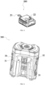
FIG. 5 is a schematic view of a battery pack according to an example of the present application. -
FIG. 6 is a schematic view of a PCB according to an example of the present application. - Before any examples of this application are explained in detail, it is to be understood that this application is not limited to its application to the structural details and the arrangement of components set forth in the following description or illustrated in the above drawings.
- In this application, the terms "comprising", "including", "having" or any other variation thereof are intended to cover an inclusive inclusion such that a process, method, article or device comprising a series of elements includes not only those series of elements, but also other elements not expressly listed, or elements inherent in the process, method, article, or device. Without further limitations, an element defined by the phrase "comprising a ..." does not preclude the presence of additional identical elements in the process, method, article, or device comprising that element.
- In this application, the term "and/or" is a kind of association relationship describing the relationship between associated objects, which means that there can be three kinds of relationships. For example, A and/or B can indicate that A exists alone, A and B exist simultaneously, and B exists alone. In addition, the character "/" in this application generally indicates that the contextual associated objects belong to an "and/or" relationship.
- In this application, the terms "connection", "combination", "coupling" and "installation" may be direct connection, combination, coupling or installation, and may also be indirect connection, combination, coupling or installation. Among them, for example, direct connection means that two members or assemblies are connected together without intermediaries, and indirect connection means that two members or assemblies are respectively connected with at least one intermediate members and the two members or assemblies are connected by the at least one intermediate members. In addition, "connection" and "coupling" are not limited to physical or mechanical connections or couplings, and may include electrical connections or couplings.
- In this application, it is to be understood by those skilled in the art that a relative term (such as "about", "approximately", and "substantially") used in conjunction with quantity or condition includes a stated value and has a meaning dictated by the context. For example, the relative term includes at least a degree of error associated with the measurement of a particular value, a tolerance caused by manufacturing, assembly, and use associated with the particular value, and the like. Such relative term should also be considered as disclosing the range defined by the absolute values of the two endpoints. The relative term may refer to plus or minus of a certain percentage (such as 1%, 5%, 10%, or more) of an indicated value. A value that did not use the relative term should also be disclosed as a particular value with a tolerance. In addition, "substantially" when expressing a relative angular position relationship (for example, substantially parallel, substantially perpendicular), may refer to adding or subtracting a certain degree (such as 1 degree, 5 degrees, 10 degrees or more) to the indicated angle.
- In this application, those skilled in the art will understand that a function performed by an assembly may be performed by one assembly, multiple assemblies, one member, or multiple members. Likewise, a function performed by a member may be performed by one member, an assembly, or a combination of members.
- In this application, the terms "up", "down", "left", "right", "front", and "rear" " and other directional words are described based on the orientation or positional relationship shown in the drawings, and should not be understood as limitations to the examples of this application. In addition, in this context, it also needs to be understood that when it is mentioned that an element is connected "above" or "under" another element, it can not only be directly connected "above" or "under" the other element, but can also be indirectly connected "above" or "under" the other element through an intermediate element. It should also be understood that orientation words such as upper side, lower side, left side, right side, front side, and rear side do not only represent perfect orientations, but can also be understood as lateral orientations. For example, lower side may include directly below, bottom left, bottom right, front bottom, and rear bottom.
- In this application, the terms "controller", "processor", "central processor", "CPU" and "MCU" are interchangeable. Where a unit "controller", "processor", "central processing", "CPU", or "MCU" is used to perform a specific function, the specific function may be implemented by a single aforementioned unit or a plurality of the aforementioned unit.
- In this application, the term "device", "module" or "unit" may be implemented in the form of hardware or software to achieve specific functions.
- In this application, the terms "computing", "judging", "controlling", "determining", "recognizing" and the like refer to the operations and processes of a computer system or similar electronic computing device (e.g., controller, processor, etc.).
- As shown in
FIG. 1 , the present invention provides a power tool. InFIG. 1 , thepower tool 100 is an electric drill. However, it is to be understood that the present application is not limited to the disclosed examples but may be applied to other types ofpower tools 100, for example, a hedge trimmer, or a sander. Alternatively, thepower tool 100 may be a table tool, for example, a table saw or a miter saw. Alternatively, thepower tool 100 may be a push power tool, for example, a push mower or a push snow thrower. Alternatively, thepower tool 100 may be a riding power tool, for example, a riding mower, a riding vehicle, or an all-terrain vehicle. Alternatively, thepower tool 100 may be a robotic tool, for example, a robotic mower or a robotic snow thrower. In some examples, thepower tool 100 may be an electric drill, an electric vehicle, or the like. In some examples, thepower tool 100 may be a garden tool, for example, a hedge trimmer, a blower, a mower, or a chainsaw. Alternatively, thepower tool 100 may be a decorating tool, for example, a screwdriver, a nail gun, a circular saw, or a sander. In some examples, thepower tool 100 may be a vegetation care tool, for example, a string trimmer, a mower, a hedge trimmer, or a chainsaw. Alternatively, thepower tool 100 may be a cleaning tool, for example, a blower, a snow thrower, or a cleaning machine. Alternatively, thepower tool 100 may be a drilling tool, for example, a drill, a screwdriver, a wrench, or an electric hammer. Alternatively, thepower tool 100 may be a sawing tool, for example, a reciprocating saw, a jigsaw, or a circular saw. Alternatively, thepower tool 100 may be a table tool, for example, a table saw, a miter saw, a metal cutter, or an electric router. Alternatively, thepower tool 100 may be a sanding tool, for example, an angle grinder or a sander. Alternatively, thepower tool 100 may be another tool, for example, a machine tool or a fan. - The
power tool 100 includes anelectric motor 12, anoutput portion 11, ahousing 10, and at least onePCB 4. Theelectric motor 12 includes adrive shaft 121 rotating about adrive axis 101. Theoutput portion 11 is driven by theelectric motor 12 to output power. Thehousing 10 is used for accommodating theelectric motor 12. At least onePCB 4 is electrically connected to theelectric motor 12. In this example, the PCB may be a control board of theelectric motor 12 or a control board of other additional functions in thepower tool 100, for example, an illumination circuit board or a switch circuit board light. Here, the case where the PCB is the control board of theelectric motor 12 is used as an example for description. Various electronic components of theelectric motor 12 control circuit may be electrically coupled to the PCB so that at least the start and stop, forward and reverse rotation, and the rotational speed of theelectric motor 12 can be controlled, thereby driving theoutput portion 11 to output a driving force to drive the tool accessory to work, for example, to drive the drill bit to drill holes. ThePCB 4 is used as the control center of thepower tool 100, and many electronic components are disposed on thePCB 4. Therefore, during the manufacturing process, the surface of thePCB 4 needs to be protected. The surface protection of thePCB 4 of the current product adopts the manual hand brushing process with G6 silicone. This method is inefficient, lots of glue materials are wasted, and excess glue on the appearance inspection station needs to be removed, making the process more complicated. - To solve the preceding problems, in the examples of the present application, the automated device is used to adopt 3D printing technologies to accurately coat regions to be protected on the
PCB 4, and 3D printed protective layers42 may be stacked layer by layer so that the manual glue brushing process is replaced, thereby greatly improving the efficiency and reducing material waste. - In an example, an image or graphic of the to-be-sprayed region of the PCB to be sprayed with a protective layer may be preset in the 3D printing automated device. After the PCB is placed at a preset position, the automated device can spray the to-be-protected region with the protective material in response to a printing operation. In this example, the spraying accuracy of the automated device when the 3D printing of the protective layer is performed can reach 0.3 mm or higher. The present application does not provide any further explanation on the automated device for implementing automated 3D printing technologies.
- In this example, a 3D printed
protective layer 42 may be applied to at least one PCB in thepower tool 100. For example, the PCB to which the 3D printedprotective layer 42 needs to be applied may be selected according to the complexity of the component arrangement or the number of components on the PCB. - In an example, the thickness of the 3D printed
protective layer 42 is greater than or equal to 20 µm and less than or equal to 2000 µm, or greater than or equal to 30 µm and less than or equal to 1000 µm, or greater than or equal to 20 µm and less than or equal to 500 µm, or greater than or equal to 20 µm, for example, 30 µm, 31 µm, 32 µm, 35 µm, ..., 50 µm, 51 µm, 52 µm ... In an example, the thickness of the 3D printedprotective layer 42 is greater than 25 µm or greater than or equal to 35 µm. By adopting 3D printing technologies, ultraviolet light-emitting diode (UV-LED) solidifies and stacks the glue layer by layer, thereby achieving three-proof (mildew-proof, moistureproof, and salt spray-proof) potting and other protective effects. Moreover, by accurately controlling the thickness of the 3D printedprotective layer 42, while the encapsulation protective effect is ensured, the used glue is reduced. Moreover, after UV-LED printing, the protective layer immediately solidifies and forms a 3D printedprotective layer 42 without waiting for solidifying, masking, carriers, and other processes. Moreover, two layers of spray coatings can satisfy general requirements, thereby achieving the thin-layer coating. - In some examples, at least two
regions PCB 4 are covered with the 3D printedprotective layer 42 with different thicknesses. ThePCB 4 may be divided into different functional regions according to actual requirements, and the thickness of the 3D printedprotective layer 42 may be set according to the different functional regions, thereby satisfying the requirements of flexible encapsulation and protection of the different functional regions. Moreover, when thePCB 4 is covered with the 3D printedprotective layer 42, the glue is accurately sprayed to the position that requires protection without overflowing or splashing, thereby saving materials. - In some examples, a region on the
PCB 4 is covered with a 3D printedenclosure layer 41. By printing theenclosure layer 41, adjacent components in different functional regions can be separated so that when the functional regions are subsequently covered and encapsulated, the glue is only in the region formed by theenclosure layer 41 and does not flow to other functional regions, thereby ensuring a smooth encapsulation process. When theenclosure layer 41 is printed, the height of theenclosure layer 41 needs to be set according to the heights and distances of the components disposed on thePCB 4. After theenclosure layer 41 is printed, the region enclosed by theenclosure layer 41 is filled. Moreover, theenclosure layer 41 can achieve waterproof sealing so that the housing does not need to be provided. - In some examples, the region enclosed by the
enclosure layer 41 is capable of being covered with aprotective layer 411 different from the 3D printedprotective layer 42. For thePCB 4 with higher requirements for local components, the components encapsulated by the enclosure layer may be filled with glue with better protection performance, and UV glue may be used to cover other components, thereby achieving different levels of local protection and achieving a balance between efficiency and reliability. - In some examples, the 3D printed
protective layer 42 is formed by spraying thePCB 4 multiple times. By stacking multiple layers of spray coatings, a thicker 3D printedprotective layer 42 can be obtained, thereby forming a 3D shape with a certain mechanical strength to satisfy the high protection requirements of products. - In some examples, the thickness of a single-layer spray coating is greater than or equal to 20 µm, for example, 25 µm, 28 µm, 30 µm, 32 µm, 35 µm, ... By setting the thickness of a single-layer spray coating, general protection requirements can be satisfied after two layers are sprayed so that both the efficiency of single-layer spraying and the solidification of the glue are ensured, thereby achieving efficient encapsulation and protection.
- As shown in
FIGS. 2 to 4 , in some examples, apower device 200 is further provided. Thepower device 200 may be, but is not limited to, an inverter, an adapter, or a charger. The inverter is a converter that converts direct current (DC) into alternating current (AC). The charger may convert AC into DC or may step down or step up the voltage of DC power and supply the DC power to a charging device. The adapter is an interface converter, may be a separate hardware interface device that allows the hardware or electronic interface to be connected to other hardware or electronic interfaces, or may be an information interface. For example, the adapter may be a power adapter, a tripod base adapter component, an adapter between the Universal Serial Bus (USB) and the serial port, or the like. The adapter is the power conversion device for a small portable electronic device and an electronic appliance. - In some examples, the
power device 200 includes a mountinghousing 20, afirst connection terminal 21, asecond connection terminal 22, and at least onePCB 4. The mountinghousing 20 has a mounting cavity. Thefirst connection terminal 21 is fixedly disposed in the mountinghousing 20 and electrically connected to an external power supply. Thesecond connection terminal 22 is disposed in the mountinghousing 20 and used for outputting electrical energy. ThePCB 4 is electrically connected to both thefirst connection terminal 21 and thesecond connection terminal 22. ThePCB 4 can implement functions such as AC/DC conversion, voltage bucking, and voltage boosting. ThePCB 4 is used as the control center of thepower device 200, so the surface of thePCB 4 needs to be protected during the manufacturing process. The surface protection of thePCB 4 of the current product adopts the manual hand brushing process with G6 silicone. This method is inefficient, lots of glue materials are wasted, and excess glue on the appearance inspection station needs to be removed, making the process more complicated. - To solve the preceding problem, in some examples, at least part of the at least one
PCB 4 is covered with a 3D printedprotective layer 42. The automated device is used to adopt 3D printing technologies to accurately coat regions to be protected on thePCB 4, and 3D printedprotective layers 42 may be stacked layer by layer so that the manual glue brushing process is replaced, thereby greatly improving the efficiency and reducing material waste. - In some examples, at least two
regions PCB 4 are covered with the 3D printedprotective layer 42 with different thicknesses. ThePCB 4 may be divided into different functional regions according to actual requirements, and the thickness of the 3D printedprotective layer 42 may be set according to the different functional regions, thereby satisfying the requirements of flexible encapsulation and protection of the different functional regions. Moreover, when thePCB 4 is covered with the 3D printedprotective layer 42, the glue is accurately sprayed to the position that requires protection without overflowing or splashing, thereby saving materials. - In some examples, any region on the
PCB 4 is covered with the 3D printedenclosure layer 41. By printing theenclosure layer 41, adjacent components in different functional regions can be separated so that when the functional regions are subsequently covered and encapsulated, the glue is only in the region formed by theenclosure layer 41 and does not flow to other functional regions, thereby ensuring a smooth encapsulation process. When theenclosure layer 41 is printed, the height of theenclosure layer 41 needs to be set according to the heights and distances of the components disposed on thePCB 4. After theenclosure layer 41 is printed, the region enclosed by theenclosure layer 41 is filled. Moreover, theenclosure layer 41 can achieve waterproof sealing so that the housing does not need to be provided. - In some examples, the region enclosed by the
enclosure layer 41 is capable of being covered with a protective layer different from the 3D printedprotective layer 42. For thePCB 4 with higher requirements for local components, the components encapsulated by the enclosure layer may be filled with glue with better protection performance, and UV glue may be used to cover other components, thereby achieving different levels of local protection and achieving a balance between efficiency and reliability. - In some examples, the 3D printed
protective layer 42 is formed by spraying thePCB 4 multiple times. By stacking multiple layers of spray coatings, a thicker 3D printedprotective layer 42 can be obtained, thereby forming a 3D shape with a certain mechanical strength to satisfy the high protection requirements of products. - In some examples, the thickness of a single-layer spray coating is greater than or equal to 20 µm, for example, 25 µm, 28 µm, 30 µm, 32 µm, 35 µm, ... By setting the thickness of a single-layer spray coating, general protection requirements can be satisfied after two layers are sprayed so that both the efficiency of single-layer spraying and the solidification of the glue are ensured, thereby achieving efficient encapsulation and protection.
- In some examples, a
battery pack 300 is further provided. In the example of the present application, thebattery pack 300 may be a liquid lithium-ion battery with apolymer housing 10, a pouch battery, or a hard pack battery using hard materials as abattery housing 10. For example, thehousing 10 of the hard pack battery may be made of plastic, steel, or aluminum.Battery cells 33 in thebattery pack 300 may be cylindrical cells, square cells, or sheet cells. Thebattery pack 300 may be a lithium iron phosphate battery, a ternary lithium battery, a sodium-ion battery, or the like. - As shown in
FIGS. 5 and6 , in some examples, thebattery pack 300 includes ahousing 30, cells, and at least onePCB 4. Thehousing 30 has an accommodation cavity. The cells are disposed in the accommodation cavity. ThePCB 4 is electrically connected to the cells. Further, thebattery pack 300 is provided with apower terminal 31 and acommunication terminal 32. Thepower terminal 31 is used for transmitting power. Thecommunication terminal 32 is used for transmitting communication data. ThePCB 4 is electrically connected to thepower terminal 31 and thecommunication terminal 32 and can perform discharge control or charge control. ThePCB 4 is used as the control center of thebattery pack 300, so the surface of thePCB 4 needs to be protected during the manufacturing process. The surface protection of thePCB 4 of the current product adopts the manual hand brushing process with G6 silicone. This method is inefficient, lots of glue materials are wasted, and excess glue on the appearance inspection station needs to be removed, making the process more complicated. - To solve the preceding problem, in some examples, at least part of the at least one
PCB 4 is covered with a 3D printedprotective layer 42. The automated device is used to adopt 3D printing technologies to accurately coat regions to be protected on thePCB 4, and 3D printedprotective layers 42 may be stacked layer by layer so that the manual glue brushing process is replaced, thereby greatly improving the efficiency and reducing material waste. - In some examples, at least two
regions PCB 4 are covered with the 3D printedprotective layer 42 with different thicknesses. ThePCB 4 may be divided into different functional regions according to actual requirements, and the thickness of the 3D printedprotective layer 42 may be set according to the different functional regions, thereby satisfying the requirements of flexible encapsulation and protection of the different functional regions. Moreover, when thePCB 4 is covered with the 3D printedprotective layer 42, the glue is accurately sprayed to the position that requires protection without overflowing or splashing, thereby saving materials. - In some examples, any region on the
PCB 4 is covered with the 3D printedenclosure layer 41. By printing theenclosure layer 41, adjacent components in different functional regions can be separated so that when the functional regions are subsequently covered and encapsulated, the glue is only in the region formed by theenclosure layer 41 and does not flow to other functional regions, thereby ensuring a smooth encapsulation process. When theenclosure layer 41 is printed, the height of theenclosure layer 41 needs to be set according to the heights and distances of the components disposed on thePCB 4. After theenclosure layer 41 is printed, the region enclosed by theenclosure layer 41 is filled. Moreover, theenclosure layer 41 can achieve waterproof sealing so that the housing does not need to be provided. - In some examples, the region enclosed by the
enclosure layer 41 is capable of being covered with a protective layer different from the 3D printedprotective layer 42. For thePCB 4 with higher requirements for local components, the components encapsulated by the enclosure layer may be filled with glue with better protection performance, and UV glue may be used to cover other components, thereby achieving different levels of local protection and achieving a balance between efficiency and reliability. - In some examples, the 3D printed
protective layer 42 is formed by spraying thePCB 4 multiple times. By stacking multiple layers of spray coatings, a thicker 3D printedprotective layer 42 can be obtained, thereby forming a 3D shape with a certain mechanical strength to satisfy the high protection requirements of products. - In some examples, the thickness of a single-layer spray coating is greater than or equal to 20 µm, for example, 25 µm, 28 µm, 30 µm, 32 µm, 35 µm, ... By setting the thickness of a single-layer spray coating, general protection requirements can be satisfied after two layers are sprayed so that both the efficiency of single-layer spraying and the solidification of the glue are ensured, thereby achieving efficient encapsulation and protection.
- The basic principles, main features, and advantages of this application are shown and described above. It is to be understood by those skilled in the art that the aforementioned examples do not limit the present application in any form, and all technical solutions obtained through equivalent substitutions or equivalent transformations fall within the scope of the present application.
Claims (15)
- A power tool (100), comprising:an electric motor (12) comprising a drive shaft (121) rotating about a drive axis (101);an output portion (11) driven by the electric motor to output power;a housing (10) for accommodating the electric motor; andat least one print circuit board (PCB) (4) electrically connected to the electric motor, wherein at least part of the at least one PCB (4) is covered with a three-dimensional (3D) printed protective layer (42).
- The power tool of claim 1, wherein a thickness of the 3D printed protective layer is greater than or equal to 20 µm and less than or equal to 2000 µm.
- The power tool of claim 1, wherein at least two regions (431, 432) on a PCB (4) of the at least one PCB (4) are covered with the 3D printed protective layer with different thicknesses.
- The power tool of claim 1, wherein a region on a PCB (4) of the at least one PCB (4) is covered with a 3D printed enclosure layer (41).
- The power tool of claim 4, wherein a region enclosed by the enclosure layer (41) is capable of being covered with a protective layer (411) different from the 3D printed protective layer.
- The power tool of claim 1, wherein the 3D printed protective layer is formed by spraying a PCB (4) of the at least one PCB (4) multiple times.
- The power tool of claim 6, wherein a thickness of a single-layer spray coating is greater than or equal to 20 µm.
- A power device (200), comprising:a mounting housing (20) having a mounting cavity;a first connection terminal (21) disposed in the mounting housing (20) and electrically connected to an external power supply;a second connection terminal (22) disposed in the mounting housing (20) and used for outputting electrical energy to a battery pack (300) capable of supplying power to a power tool (100); andat least one print circuit board (PCB) (4) electrically connected to both the first connection terminal (21) and the second connection terminal (22), wherein at least part of the at least one PCB (4) is covered with a three-dimensional (3D) printed protective layer.
- The power device of claim 8, wherein at least two regions (431, 432) on a PCB (4) of the at least one PCB (4) are covered with the 3D printed protective layer with different thicknesses.
- The power device of claim 8, wherein a region on a PCB (4) of the at least one PCB (4) is covered with a 3D printed enclosure layer (41).
- The power device of claim 10, wherein a region enclosed by the enclosure layer (41) is capable of being covered with a protective layer (411) different from the 3D printed protective layer.
- The power device of claim 8, wherein the 3D printed protective layer is formed by spraying a PCB (4) of the at least one PCB (4) multiple times.
- The power device of claim 12, wherein a thickness of a single-layer spray coating is greater than or equal to 20 µm.
- A battery pack (300) capable of supplying power to a power tool (100), comprising:a housing (30) having an accommodation cavity;a cell (33) disposed in the accommodation cavity; andat least one print circuit board (PCB) (4) electrically connected to the cell, wherein at least part of the at least one PCB (4) is covered with a three-dimensional (3D) printed protective layer.
- The battery pack of claim 14, wherein at least two regions (431, 432) on a PCB (4) of the at least one PCB (4) are covered with the 3D printed protective layer with different thicknesses.
Applications Claiming Priority (1)
| Application Number | Priority Date | Filing Date | Title |
|---|---|---|---|
| CN202311788977.XA CN120239189A (en) | 2023-12-22 | 2023-12-22 | Power tools, power supply units and battery packs |
Publications (1)
| Publication Number | Publication Date |
|---|---|
| EP4574343A1 true EP4574343A1 (en) | 2025-06-25 |
Family
ID=93284055
Family Applications (1)
| Application Number | Title | Priority Date | Filing Date |
|---|---|---|---|
| EP24208530.6A Pending EP4574343A1 (en) | 2023-12-22 | 2024-10-24 | Power tool |
Country Status (4)
| Country | Link |
|---|---|
| US (1) | US20250212338A1 (en) |
| EP (1) | EP4574343A1 (en) |
| CN (1) | CN120239189A (en) |
| AU (1) | AU2024264581A1 (en) |
Citations (6)
| Publication number | Priority date | Publication date | Assignee | Title |
|---|---|---|---|---|
| DE102014113990A1 (en) * | 2014-09-26 | 2016-03-31 | Endress + Hauser Gmbh + Co. Kg | Method for protecting at least one predetermined subarea of a printed circuit board equipped with at least one component |
| EP3576503A1 (en) * | 2018-05-31 | 2019-12-04 | Airbus Operations, S.L. | Implementation process of a humidity control sensor for 3d-printing of a smart tool and process for manufacturing a humidity control sensor via 3d-printing technology |
| DE102019220202A1 (en) * | 2019-12-19 | 2021-06-24 | Robert Bosch Gmbh | Battery device for a battery pack of a hand machine tool |
| WO2021155156A1 (en) * | 2020-01-30 | 2021-08-05 | Milwaukee Electric Tool Corporation | Automatic step bit detection |
| US20230094289A1 (en) * | 2021-09-10 | 2023-03-30 | Continental Automotive Systems, Inc. | 3d-printed, pcb composite structures, and formation methods |
| DE202023103553U1 (en) * | 2022-06-27 | 2023-09-18 | Milwaukee Electric Tool Corporation | Device with a fuse |
-
2023
- 2023-12-22 CN CN202311788977.XA patent/CN120239189A/en active Pending
-
2024
- 2024-10-24 EP EP24208530.6A patent/EP4574343A1/en active Pending
- 2024-10-25 US US18/927,149 patent/US20250212338A1/en active Pending
- 2024-11-12 AU AU2024264581A patent/AU2024264581A1/en active Pending
Patent Citations (6)
| Publication number | Priority date | Publication date | Assignee | Title |
|---|---|---|---|---|
| DE102014113990A1 (en) * | 2014-09-26 | 2016-03-31 | Endress + Hauser Gmbh + Co. Kg | Method for protecting at least one predetermined subarea of a printed circuit board equipped with at least one component |
| EP3576503A1 (en) * | 2018-05-31 | 2019-12-04 | Airbus Operations, S.L. | Implementation process of a humidity control sensor for 3d-printing of a smart tool and process for manufacturing a humidity control sensor via 3d-printing technology |
| DE102019220202A1 (en) * | 2019-12-19 | 2021-06-24 | Robert Bosch Gmbh | Battery device for a battery pack of a hand machine tool |
| WO2021155156A1 (en) * | 2020-01-30 | 2021-08-05 | Milwaukee Electric Tool Corporation | Automatic step bit detection |
| US20230094289A1 (en) * | 2021-09-10 | 2023-03-30 | Continental Automotive Systems, Inc. | 3d-printed, pcb composite structures, and formation methods |
| DE202023103553U1 (en) * | 2022-06-27 | 2023-09-18 | Milwaukee Electric Tool Corporation | Device with a fuse |
Also Published As
| Publication number | Publication date |
|---|---|
| AU2024264581A1 (en) | 2025-07-10 |
| US20250212338A1 (en) | 2025-06-26 |
| CN120239189A (en) | 2025-07-01 |
Similar Documents
| Publication | Publication Date | Title |
|---|---|---|
| EP2342805B1 (en) | Power tool | |
| JP2012091293A (en) | Power tool system | |
| EP3683935B1 (en) | Power module for a brushless motor in a power tool | |
| JPWO2020137911A1 (en) | Electric work machine | |
| EP4429003A1 (en) | Power tool and battery pack | |
| EP4574343A1 (en) | Power tool | |
| JP7190511B2 (en) | electric work machine | |
| WO2017082082A1 (en) | Electric tool | |
| CN101115587A (en) | Handheld Power Tools | |
| CN221928340U (en) | Battery pack for powering electronic devices | |
| EP4497991A1 (en) | Illumination device | |
| CN221552036U (en) | Battery packs for powering electronic devices | |
| EP1485169B1 (en) | Hydraulic rescue tool supplied by a battery | |
| EP4650101A1 (en) | Pole power tool | |
| CN213195587U (en) | Combined tool head | |
| CN212216117U (en) | Tray for gluing lead storage battery cover | |
| US20250167630A1 (en) | Power tool and battery pack thereof | |
| US20250346127A1 (en) | Outdoor work vehicle | |
| CN118596090A (en) | Power tools and battery packs | |
| EP4454816B1 (en) | Impact tool | |
| CN204886575U (en) | Three -phase brushless DC motor | |
| CN222095837U (en) | Adjustable tray is used in production of P single-edge milling cutter | |
| EP4626162A1 (en) | Electric tool | |
| CN219254772U (en) | Portable three-dimensional numerical control self-positioning machining device | |
| US20250337032A1 (en) | Battery pack for powering a power tool |
Legal Events
| Date | Code | Title | Description |
|---|---|---|---|
| PUAI | Public reference made under article 153(3) epc to a published international application that has entered the european phase |
Free format text: ORIGINAL CODE: 0009012 |
|
| STAA | Information on the status of an ep patent application or granted ep patent |
Free format text: STATUS: THE APPLICATION HAS BEEN PUBLISHED |
|
| AK | Designated contracting states |
Kind code of ref document: A1 Designated state(s): AL AT BE BG CH CY CZ DE DK EE ES FI FR GB GR HR HU IE IS IT LI LT LU LV MC ME MK MT NL NO PL PT RO RS SE SI SK SM TR |
|
| STAA | Information on the status of an ep patent application or granted ep patent |
Free format text: STATUS: REQUEST FOR EXAMINATION WAS MADE |
|
| 17P | Request for examination filed |
Effective date: 20251110 |