EP4572006A1 - Translucent antenna foil comprising an antenna mounted on an optical element - Google Patents
Translucent antenna foil comprising an antenna mounted on an optical element Download PDFInfo
- Publication number
- EP4572006A1 EP4572006A1 EP23216558.9A EP23216558A EP4572006A1 EP 4572006 A1 EP4572006 A1 EP 4572006A1 EP 23216558 A EP23216558 A EP 23216558A EP 4572006 A1 EP4572006 A1 EP 4572006A1
- Authority
- EP
- European Patent Office
- Prior art keywords
- antenna
- foil
- optical element
- light
- connector
- Prior art date
- Legal status (The legal status is an assumption and is not a legal conclusion. Google has not performed a legal analysis and makes no representation as to the accuracy of the status listed.)
- Pending
Links
Images
Classifications
-
- H—ELECTRICITY
- H01—ELECTRIC ELEMENTS
- H01Q—ANTENNAS, i.e. RADIO AERIALS
- H01Q1/00—Details of, or arrangements associated with, antennas
- H01Q1/12—Supports; Mounting means
- H01Q1/22—Supports; Mounting means by structural association with other equipment or articles
-
- H—ELECTRICITY
- H01—ELECTRIC ELEMENTS
- H01Q—ANTENNAS, i.e. RADIO AERIALS
- H01Q1/00—Details of, or arrangements associated with, antennas
- H01Q1/08—Means for collapsing antennas or parts thereof
- H01Q1/085—Flexible aerials; Whip aerials with a resilient base
-
- H—ELECTRICITY
- H01—ELECTRIC ELEMENTS
- H01Q—ANTENNAS, i.e. RADIO AERIALS
- H01Q1/00—Details of, or arrangements associated with, antennas
- H01Q1/36—Structural form of radiating elements, e.g. cone, spiral, umbrella; Particular materials used therewith
- H01Q1/364—Structural form of radiating elements, e.g. cone, spiral, umbrella; Particular materials used therewith using a particular conducting material, e.g. superconductor
-
- H—ELECTRICITY
- H01—ELECTRIC ELEMENTS
- H01Q—ANTENNAS, i.e. RADIO AERIALS
- H01Q7/00—Loop antennas with a substantially uniform current distribution around the loop and having a directional radiation pattern in a plane perpendicular to the plane of the loop
Definitions
- the invention relates to a translucent antenna foil mounted on an optical element of a device, with none or at most minor negative effect on a respective optical light path desired for the respective optical element.
- antennas are also known, whereas hereby these antennas are either fixedly integrated inside the respective optical element or are inflexible and stiff extra components that mounted inside of a respective housing of a device.
- this arrangement is often regarded as disadvantage with regard to a uniform light distribution.
- the EP 3 320 581 B1 deals with such an extra antenna device being mounted cantered inside a luminaire on a printed circuit board.
- an antenna is described that is fixedly connected to a respective flexible printed circuit board, whereas the antenna is disposed on a surface of a light guide plate of a light-emitting device, and the light-emitting device emits light on the basis of identification information obtained through communications via antenna.
- the US 2009/0047900 A1 describes a repeater system that is designed to amplify mobile radio communications, particularly through metallised window panes, whereas hereby an outside and inside antenna are required that are connected, whereas the inside antenna is integrated inside the respective window and retransmits signals received from the outside antenna.
- these known antennas are not suitable for applications in which an antenna is to be flexibly arranged in or on optical elements of any shape.
- the invention is concerned with the task of providing a flexible antenna for flexible use in optical elements applications.
- This task is solved by the translucent antenna foil comprising an antenna, for use in a device having an optical element according to independent claim 1.
- the invention is defined in the independent claims. Additional features of the invention are provided in the respective dependent claims.
- the translucent antenna foil comprising an antenna, for use in a device having an optical element, is mountable on or in the optical element of the respective device, and has an antenna portion and a feeder line portion.
- an antenna conductor of the antenna for emitting and receiving signals is positioned in the antenna portion
- the feeder line portion includes a connector having respective contacts for coupling the antenna to a complementary connector on a circuit board of the device, and a connecting portion connecting the antenna conductor and the connector.
- both the antenna portion and the feeder line portion are substantially translucent.
- the translucent antenna foil allows for a positioning of the antenna in convenient positions of the respective device, minimizing influence of other components of the device on the signal communication towards and from the antenna.
- the translucent antenna foil itself also a kit consisting of the translucent antenna foil and a respective optical element on which the antenna foil is mounted is disclosed herein. Additional features relating to the antenna foil and/or the optical element thus are also valid for the combined assembly.
- the device comprises an optical element, a circuit board and a housing, whereas the optical element and the circuit board are arranged on an inside of the device.
- the device further comprises a light emitting element, such as an LED, or a light receiving element, such as a sensor element, or respectively multiple thereof wherein the device further comprises the antenna foil according to any one of the herein disclosed embodiments of the translucent antenna foil.
- the optical element is made of plastic and/or glass and the antenna foil is mounted on and/or in the optical element.
- the antenna foil is coupled via its connector to the circuit board. With the respective antenna foil in use, the user of the device may not detect the foil per se, with its respective translucent characteristics, increasing the devices aesthetics.
- the one or multiple light emitting elements may be positioned on an LED-module (or multiple LED-modules), whereas it is also conceivable that respectively one or multiple OLEDs are used as the light emitting element(s), or the like.
- the such configured device benefits from the advantages of the translucent antenna foil, as the light emission or light absorption (respectively light intake) of the device is not influenced in an unwanted way.
- the translucent antenna foil can also aid in light manipulation, e.g., when a light homogenization is desired via a diffusing characteristic of the translucent antenna foil, or the like.
- a beneficial signal transmission towards and from the antenna of the device is achieved, as the antenna is arranged on or in the optical element, and not, e.g., on a printed circuit board of the device or inside the (often metallic) housing of the device, reducing the influence of jamming sources.
- the antenna foil comprises an electrically conductive middle layer and two laminated foil layers, sandwiching the middle layer.
- the electrically conductive middle layer comprises the antenna conductor.
- the conductive middle layer respectively the antenna, is protected against outside influences.
- the two laminated foil layers hereby provide a continuous insulation up to the plug (i.e., the connector) due to the two foil layers being laminated on both sides encapsulating the middle layer. This results in an utmost durable, flexibly applicable antenna foil.
- both the antenna portion and the feeder line portion are formed by the two laminated foil layers, and the conductive middle layer arranged between the two foil layers.
- both the feeder line portion and the antenna portion are equally durable yet flexible, and furthermore the middle layer is particularly protected from outside influences.
- a non-conductive filler material for example an insulator, may be provided in the middle layer between adjacent segments of the antenna conductor and further preferred also in edge regions of the antenna foil.
- an improved electric isolation of different segments of the antenna is achieved.
- the non-conductive filler is ideally not present at the end face of the connector, such that an ideal electrical coupling of the plug with the respective counterpart is possible.
- the feeder line portion optionally in an end region of the feeder line portion only one of the two laminated foil layers, is present, and thus in this end region the conductive middle layer is uncovered forming the contacts of the connector of the feeder line portion.
- the conductive middle layer is uncovered forming the contacts of the connector of the feeder line portion.
- an easy but effective connection of the antenna with the device is achievable.
- a reinforcing layer is provided on top of the only foil layer.
- the feeder line portion and in particular the connector is reinforced, forming it more durable and easy to connect to the respective opposite connection mean of the device.
- the uncovered segments of the antenna conductor are provided with a metal print, preferably with a silver print and/or a gold print and/or a copper print and/or by plasma metallization, forming the contacts of the connector of the feeder line portion. This improves signal transmission of the antenna due to reduction of losses at the connector interface between the antenna foil and the device by the selected metal material and protects the conductive layer.
- the antenna conductor comprises copper. This improves antenna characteristics of the antenna foil, while simultaneously ensuring a flexible but still durable foil. Hence, it is preferred that the antenna foil is made flexible and in particular reversibly bendable. This ensures applicability of the foil in various scenarios and further ensures different application scenarios over its lifetime.
- the antenna foil is substantially transparent and preferably has a degree of transparency of at least 90%. This allows the antenna to be positioned on optical elements where direct and ultimately lossless light transmittal is important.
- the antenna foil itself has a light-diffusing effect, and preferably is opaque.
- the foil itself may be arranged on an optical element that is a diffusor, and hereby may also improve diffusing characteristics of the optical element via synergy.
- the antenna foil hereby contributes to the desired influence on the optical path of the respective regarded emitted or received light.
- the antenna conductor is such arranged within the middle layer that it contributes to the diffusion effect. The arrangement of the various antenna segments of the antenna conductor can be aligned such that a respective diffusing effect is achieved by the foil.
- the antenna foil has, at least in the antenna portion, an adhesive layer which is arranged on one of the foil layers.
- the adhesive layer is integrally formed by one of the foil layers.
- the antenna conductor forms a wire mesh, which is formed, e.g., in a flat coil shape, wherein further preferably the wire mesh is designed for transmitting and/or receiving NFC signals or other RFID signals.
- the foil may also be designed to transmit and receive Sub-GHz, 5 GHz frequency band signals, 2.4 GHz frequency band signals, Zig-Bee signals, and/or 5G signals or RF signals with another frequency.
- the such formed antenna foil is adapted to the respective usage scenario and an optimal signal transmission and receival is obtained via the respective specific antenna wire mesh arrangement.
- the optical element together with the light emitting or light receiving element, forms an effective optical field EOF of the device, wherein at the antenna portion of the antenna foil is arranged in the device such that only components of the device made of plastic and/or glass are arranged within the effective optical field EOF between an outside O of the device and the antenna portion.
- the so formed device has a further increased accessibility for communication with a user's operating device, resulting in an easy and comfortable communication and thus maintenance of the device due to the beneficial arrangement of the antenna foil.
- the antenna portion of the antenna foil is arranged on a side of the optical element facing the light emitting or light receiving element, or wherein the antenna portion of the antenna foil is disposed inside the optical element itself.
- the disposal inside the optical element further protects the antenna foil
- the arrangement on an outer surface of the optical element further facilitates setup of the device.
- the antenna foil is coupled to the optical element by means of an adhesive element, for example by means of an adhesive layer arranged on an outer surface layer of one laminated foil layer, of the antenna foil, or wherein the antenna foil is coupled to the optical element by means of holding elements and/or guide elements, which are preferably formed by the optical element itself. While the coupling via an adhesive element further eases setup and provides a secure mounting, repositioning the antenna foil may be more complicated than the positioning via the structural elements for holding and/or guiding the foil.
- the circuit board of the device comprises control electronics components for controlling an antenna, the control electronics components also comprising the complementary connector to which the antenna foil is coupled via its connector.
- the circuit board of the device is a control electronics board for controlling an antenna.
- the antenna of the antenna foil is controlled via a distinct circuit board.
- the complementary connector is a zero insertion force, ZIF, connector. This eases assembly of the device and further increases lifespan of the antenna foil, as no force is required during connection of the connector with the complementary connector.
- the device is a luminaire
- the luminaire has a light source board having a plurality of light sources, e.g., LEDs, and wherein the optical element transmits light being emitted from the light sources.
- the light guide is a diffuser arranged subsequent to the light source board in the light emitting direction of the light sources.
- the antenna foil is arranged on or in the optical element and may therefore be arranged in-between a light emission surface of the luminaire and the light sources of the luminaire, without affecting light transmission in an unwanted manner.
- the antenna foil is preferably also designed with a diffusing characteristic improving diffusion of the luminaire.
- the circuit board of the luminaire is the control electronics board that is arranged separately from the light source board inside the luminaire.
- the control electronics board with the components for controlling the antenna of the antenna foil are separated from other circuit boards (such as the light source board) such that electromagnetic interference is minimized.
- the light source board of the luminaire also comprises control electronics components for controlling an antenna, the control electronics components also comprising the complementary connector to which the antenna foil is coupled via its connector, whereas the control electronics components are positioned on a side of the light source board that is opposite to the side on which the light sources are mounted.
- a single printed circuit board is required within the luminaire for simultaneously achieving illumination and a signal transmission and receival.
- the device is a sensor, whereas the sensor has a sensor board having at least one sensor element, wherein the optical element forms a light entry surface of the sensor, and transmits light towards the sensor element.
- the available space of the sensor is used very efficient, wherein a convenient communication mean is provided with the antenna of the antenna foil.
- the control electronics components for controlling the antenna of the antenna foil can either be provided on the same circuit board as the sensor element of the sensor, or can also be provided on a separate circuit board, as previously discussed with regard to the other embodiment of the device being a luminaire.
- the sensor is a passive infrared, PIR, motion detector, an infrared, IR, sensor, and/or a light sensor.
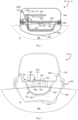
- Figure 1 shows a schematic illustration of a device 10, which may be a sensor 12 or a luminaire 11, or any other device where an optical element 200 is present and an easy and interference-free communication via the antenna foil 100 is desired.
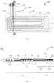
- An exemplary illustration of the antenna foil 100 itself is shown in Figures 3 and 4 .
- Figure 2 shows an exemplary embodiment of the device 10 being a luminaire 11.
- Figures 1 and 2 each show a device 10 comprising an optical element 200, at least one circuit board 300, 500 and a housing 600, 700, wherein the optical element 200 and the circuit board 300, 500 are arranged on an inside I of the device 10.
- the device 10 further comprises an antenna foil 100, which is connected to (at least) one of the circuit boards 300, 500 of the device 10.
- the antenna foil 100 is each directly linked to a control electronics board 500.
- the antenna foil 100 is positioned in an inside I of the device 10, whereby it is hereby mounted on an inside surface of the optical element 200.
- the antenna foil 100 respectively the antenna portion 110 of the antenna foil 100 is thus arranged in-between the optical element 200 and a circuit board 300 on which a light receiving element 320, such as a sensor 320, or a light emitting element 310, such as an LED 310 or LED module 310, is mounted.
- the feeder line portion 120 of the antenna foil 100 juts from the optical element 200 further inside the device 10, respectively further inside the housing 700 of the device 10.
- the antenna foil 100 may jut through a through hole 420 of the carrier element 400 (or depending on the size of the circuit board 300, also a through a respective trough hole of the circuit board 300), to further reach inside the device 10 where control electronics components 510 for controlling the antenna are positioned.
- the connection with these control electronics components 510 may be realized via a complementary connector 520 that is complementary designed to the connector 123 of the antenna foil 100.
- a control electronics board 500 is present inside the device 10, whereas the control electronics board 500 is a printed circuit board, PCB, on which the control electronics components 510 and the complementary connector 520 are positioned.
- the control electronics components 510 are hereby configured to receive the signals, which obtained by the antenna of the antenna foil 100 and provided via the connection of connectors 520 and 123, and evaluate these signals. Based on the message included in the signals the controller of the control electronics components 510 may control the light emission and/or light receiving element 310, 320, and/or may also send a respective answer signal via the antenna of the antenna foil 100.
- the internal communication between the components of the device 10 may hereby be realized via a respective internal bus interface 900.
- a light emitting or light receiving element 310, 320 is positioned onside the circuit board 300, which depending on the implementation of the device 10, may be a light source board 300 (with the device 10 being a luminaire 11) or a sensor board 300 (with the device 10 being a sensor 12) or the like.
- the light emitting or light receiving element 310, 320 hereby equally have a respective effective optical field EOF whereas the respectively present optical element 200 may also influence the effective optical field EOF depending on its light guiding characteristics.
- the optical element 200 is made of plastic and/or glass for optimal desired light guidance.
- the device 10 itself has an effective optical field EOF, which describes an area of the device 10, which is relevant for the respective light emitting or light receiving element 310, 320.
- An exemplary effective optical field EOF of the respective device 10 is schematically indicated in Figures 1 and 2 by the enclosed area of the boarder lines and the dashed lines.
- the carrier element 400 is positioned inside I of the device 10 and is preferably connected to the housing 400 of the device 10.
- the device 10 may also comprise a translucent (or even transparent) cover 600 that closes the housing in light emission and/or light receiving direction of the respective light emitting or light receiving element 310, 320.
- the cover 600 provides a certain ingress protection, forming the device 10 more durable against dust, moisture and/or water.
- the housing 700 together with the cover 600 boarder the device 10 and distinguishes in an inside I of the device 10 and an outside O of the device 10.
- the optical element 200 itself may provide at least to some degree protection to the electronic components of the device 10, and substitutes the cover 600.
- the optical element 200 is also connected to the carrier element 400, whereas as shown in Figure 1 individual connecting elements 800 may be used for reversible attachment of the optical element 200.
- These connecting elements 800 may be formed by screws, pins, a latch element or the like.
- a user being at an outside O of the device 10 operates a certain device that is equipped with a wireless communication module.
- the wireless communication module of the user device matches a signal transmission technology supported by the antenna of the antenna foil 100, such that the user device and the device 10 are able to communicate with each other.
- the antenna foil 100 With the arrangement of the antenna foil 100 being placed inside or onside the optical element 200 it is achieved that only a minimum number of elements is arranged between the antenna foil 100 and the respective user device of a user. No interference objects, in particular made out of metal are arranged in-between the antenna foil 100 on the inside I of the device 10 and the outside O of the device such that a particular favourable signal transmission is possible. As shown in Figure 1 no metal elements is arranged in-between, whereas the influence of the material of the housing of the device 10 is reduced to a minimum, and indeed can be disregarded, due to the specific arrangement and layout of the antenna foil 100.
- the effective optical field EOF of a device 10 is usually not only the area being illuminated (luminaire 11) or observed (sensor 12), but also the area where a user device is located for communication with the device 10 via its antenna.
- the antenna portion 110 of the antenna foil 100 is positioned inside the device 10 such that only components of the device 10 made of plastic and/or glass are arranged within the effective optical field EOF between the outside O of the device 10 and the antenna portion 110. This vastly reduces interferences and therefore boosts signal transmission quality and therefore also increases efficiency of the device 10.
- control electronics board 500 is mounted on a backside of the carrier element 400 - such that the control electronics board 500 is mounted on the opposite side of the carrier element 400 with regard to the light source board 300, or the respectively the sensor board 300.
- the circuit board 300 is mounted on a spacing 410 allowing the electronics components 510 and the complementary connector 520 being positioned on a backside of the circuit board 300 that is opposite to the side of the circuit board 300 having the light emitting or light receiving element 310, 320. With this implementation only one circuit board is necessary and the available space is utmost efficiently used.
- circuit boards 300, 500 can also be connected to an external power and/or communication line 1000 via a respective interface 900 that comprises respective ports on each thereto connected circuit board 300, 500.
- control electronics board 500 and/or the light source board 300 are fed with electrical energy and/or with commands regarding their operation.
- the electrical components may also communicate received and/or gathered data with external components via the interface 900 and the respective line 1000.
- FIG. 2 shows a specific implementation of the device 10 being a luminaire 11, with light emitting elements 310 being LEDs 310.
- the cover 600 is coupled via snap-fit with the housing 700 forming a durable enclosure against ingress of dust, moisture or water.
- a respective coupling 650 between the housing 700 and the cover 600 is realized by both components.
- the coupling 650 may also comprise a gasket.
- the carrier element 400 On the inside I of the shown device 10 (respectively the luminaire 11) the carrier element 400 is arranged, whereas the optical element 200 is coupled thereto as well as the control electronics board 500.
- a containment is present, in which the circuit board 300 is arranged.
- the antenna foil 100 On the side of the optical element 200 facing the circuit board 300 the antenna foil 100 is mounted.
- the circuit board 300 - which in the shown embodiment is a light source board 300 - is attached to the carrier element 400 via spacing elements 410, such that the circuit board 300 is arranged on the inside of the containment on a level of the optical element 200 that is equipped with the antenna foil 100.
- the circuit board 300 is sphered by the antenna foil 100. This results in a homogenous light emission (respectively a uniform light receival) of the device 10, as the antenna foil 100 is attached to the optical element 200 in the respective section over the relevant height.
- the feeder line portion 120 is arranged outside the effective optical field EOF such that the feeder line portion 120 does not necessarily have the same light effecting characteristic as the antenna portion 110.
- the feeder line portion 120 indeed is arranged in the effective optical field EOF - see, e.g., Figure 1 - a respectively adapted configuration is preferred.
- the optical element 200 is a diffusor.
- the antenna foil 100 is configured transparent, and in the alternative that the antenna foil 100 itself comprises light diffusing characteristics, and thus supports light diffusion of the optical element 200. If however a clean transparent optical element 200 is desired, the antenna foil 100 is ultimately also configured transparent.
- the diffusor i.e., the optical element 200
- the diffusor is hereby arranged subsequent to the light source board 300 in the light emitting direction of the light sources 310.
- the circuit board 300, 500 of the luminaire 11 to which the antenna foil 100 is connected to is the control electronics board 500 that is arranged separately from the light source board 300 inside the luminaire 11.
- the light source board 300 of the luminaire 11 also comprises control electronics components 510 for controlling an antenna, the control electronics components 510 also comprising the complementary connector 520 to which the antenna foil 100 is coupled via its connector 123.
- the control electronics components 510 are positioned on a side of the light source board 300 that is opposite to the side on which the light sources 310 are mounted.
- the cover 600 may also comprise light emission influencing elements 610 that interact with light outgoing from assembly of the light emitting element 310 and optical element 200 (or incoming light coming from outside O towards the assembly of optical element 200 and light receiving element 320). Via this cover the respective light can be adjusted with regard to a specific installation situation. It is further conceivable that the light modification characteristics of the light optical element 200, the antenna foil 100 and/or the light emission influencing elements 610 are geared to each other.
- FIGS 3 and 4 show the same exemplary embodiment of an antenna foil 100, whereas Figure 3 shows a schematic top view, and Figure 4 shows a schematic cross section through the axis A illustrated in Figure 3 .
- Each illustration shows a translucent antenna foil 100 comprising an antenna, wherein the antenna foil 100 is mountable on or in the respective optical element 200 of the device 10.
- the antenna foil 100 can be divided into two sections: an antenna portion 110 and a feeder line portion 120.
- the antenna portion 110 an antenna conductor 111 of the antenna for emitting and receiving signals is positioned, and the feeder line portion 120 includes a connector 123 having respective contacts 124 for coupling the antenna (i.e., the antenna foil 100) to a complementary connector 520 on a circuit board 300, 500 of the device 10.
- the connecting portion 122 hereby connects the antenna conductor 111 and the connector 123 of the antenna foil 100.
- Both the antenna portion 110 and the feeder line portion 120 are substantially translucent.
- the displayed antenna foil 100 comprises three layers L1, L2 and L3, with an electrically conductive middle layer L2 and two laminated foil layers L1, L3 sandwiching the middle layer L2.
- the electrically conductive middle layer L2 comprises the antenna conductor 111.
- both the antenna portion 110 and the feeder line portion 120 are substantially equally constructed, such that in each section the conductive middle layer L2 is arranged between the two foil layers L1, L3.
- a non-conductive filler material 112 for example an insulator, is provided in the middle layer L2 between adjacent segments of the antenna conductor 111, such that optimal signal transmission and receival is achieved.
- This non-conductive filler material 112 is also present in edge regions of the middle layer L2 of the antenna foil 100, such that the edge regions of the antenna foil 100 (besides the edge region with the contacts 124 of the connector 123 being present) are formed by the laminated foil layers L1, L3 and the conductive filler material 112 in-between.
- the antenna foil 100 is built utmost resistant and durable with regard to dust, moisture and water.
- the antenna conductor 111 may be present in different height regions of the conductive middle layer L2, to achieve a preferred flexibility with regard to a respective mesh formed by the antenna conductor 111.
- the non-conductive filler material 112 may cover the antenna conductor 111 throughout the whole middle layer L2.
- the non-conductive filler material 112 is (at least partly) integrally formed by the material of the two sandwiching foil layers L1, L3.
- different materials are ideally used.
- the boundaries of the different layers L1, L2, L3 are not as strict as schematically illustrated in Figure 4 , such that, e.g., the thickness of the foil layers L1, L3 may differ section wise, and hereby may be adapted to the respective thickness of the middle layer L2, or to the respective thickness of the antenna conductor 111 in the respective sections of the middle layer L2.
- FIG. 4 Also shown in Figure 4 on the right hand side is that in one end region of the feeder line portion 120 only one of the two laminated foil layers L1, L3 is present (in the displayed example, only the bottom layer L3 is present), and thus in this end region the conductive middle layer L2 is uncovered forming the contacts 124 of the connector 123 of the feeder line portion 120.
- the connector of the antenna foil 100 is formed utmost easy and at low cost, yet enabling good signal transmission due to the uncovered antenna segments of the conductive middle layer L2.
- a reinforcing layer 126 is provided on top of the only foil layer L3 that reinforces stability of the feeder line portion 120 in the area of the connector 123.
- the configuration of the contacts 124 being provided with a metal print 125 that further enhances signal transmission due to better electrical properties or better corrosion characteristics depending on the respective material used.
- the uncovered segments of the antenna conductor 111 are provided with a silver print and/or a gold print and/or a copper print, and/or a plasma metallization.
- the complementary connector 520 is preferably a zero insertion force, ZIF, connector, whereas this implementation further facilitates assembly of the device 10, and further minimizes possible damages to the antenna foil 100.
- the antenna conductor 111 preferably is made out of silver. However, copper or gold are also conceivable to be used as a material of the antenna conductor 111. With this configuration, an easy shaping of the antenna is also possible, and the respective antenna shape can be adapted to individual needs during production.
- the antenna conductor 111 forms a wire mesh, which is formed, e.g., in a flat coil shape (as indicated in Figure 3 ).
- the form of the wire mesh hereby is adapted for transmitting and/or receiving respectively desired signals, such as NFC signals or other RFID signals, Sub-GHz frequency band signals, 2.4 GHz frequency band signals, 5 GHz frequency band signals, other frequency bands signals, Zig-Bee signals, and/or 5G signals, or the like.
- the shown antenna foil 100 is further made flexible and reversibly bendable, such that a repetitive adaption to the form of a respective optical element 200 is possible without risking failure of the antenna.
- the antenna foil 100 is substantially transparent, whereas it is also conceivable that the antenna foil 100 - or at least the antenna portion 110 - has a light diffusing characteristic. If the antenna foil 100 is desired to be transparent a degree of transparency of at least 90% is preferred.
- the antenna foil 100 itself shall have a light-diffusing effect (e.g., by being opaque) this can be achieved e.g., by respective formed foil layers L1, L3.
- a light diffusing effect of the antenna foil 100 can be further achieved by a respective configuration of the middle layer L2, and in particular of the antenna conductor 111.
- segments of the antenna conductor 111 can be arranged such that the respective segments act as a light diffusor of trespassing light, such that the antenna foil 100 has a light diffusing effect.
- this can be combined in synergy with a respective configuration of the optical element 200.
- the antenna foil 100 is not inserted inside the optical element 200 and hold therein by respective fastening means, holding elements and/or guide elements that may be integrally formed by the optical element 200 itself, it is preferred that the antenna foil 100 has, at least in the antenna portion 110, an adhesive layer which is arranged on one of the foil layers L1, L3, wherein this adhesive layer may be integrally formed by the respective foil layer L1, L3. Via this adhesive layer coupling to the optical element 200 is easily performed, facilitating setup of the device 10.
- At least one of the laminated foil layers L1, L3 in the feeder line portion 120 differs from the respective laminated foil layers L1, L3 of the antenna portion 110, to the extent that the feeder line portion 120 is more stiff. With this implementation the durability of the feeder line portion 120 is increased, which might be necessary due to the slim and narrow setup of this section.
- the device 10 may also be a sensor 12, whereas the sensor 12 has a sensor board 300 with at least one sensor element 320.
- the optical element 200 hereby forms a light entry surface of the sensor 12, and transmits light towards the sensor element 320.
- the such configured sensor allows for communication via the monitoring foil 100 and further does not negatively influence the crucial light guidance of the optical element 200.
- the sensor 12 is a passive infrared, PIR, motion detector, an infrared, IR, sensor, and/or a light sensor.
- a device 10 comprises a sensor element 320 and a light source element 310 in combination, whereas it is further possible that the optical element 200 is shared between the two elements 310, 320.
- antenna foil 100 According to the invention, devices with little space are possibly with an antenna foil 100 according to the invention, as the foil requires almost no space being aligned flush on or in the respective optical element 200 of the device 10. With its respective individual light characteristics (translucent, transparent, diffusing, or the like) the antenna foil 100 further adapts ideally to the respective requirements of the device 10.
- the optical element 200 is a light guide plate for emitting light in a direction perpendicular to the light insertion direction
- light insertion into the light guide plate is realized by light emitting elements 310 being laterally arranged on front faces of the plate-shaped light guide.
- the antenna foil 100 is arranged on a surface of the light guide plate opposite to the light emission surface of the light guide plate.
- wireless communication of the luminaire 11 is improved by usage of the antenna foil 100, while the antenna foil 100 is firstly not noticeable for a user and also does not influence light emission of the luminaire 11 at all, or at least not in a negative manner.
- the antenna foil 100 and the optical element 200 are (preferably reversibly) insertable inside the optical element 200, whereas due to its foil characteristics the antenna foil 100 adapts to the respective shape of the optical element 200.
- the optical element 200 may comprise respective rail elements on the inside which guide and preferably also hold the antenna foil 100 in place. This allows for situational adaption of the antenna foil 100 with regard to the respectively needed signal transmission type.
- the communication line realized via the antenna foil 100 may be used for integration of the respective device 10 inside an existing system, for initial setup of the device 10, maintenance, and/or other checkups.
- the kit assembly of the antenna foil 100 and the optical element 200, respectively the device 10 comprising the kit an utmost easy and interference-free communication between a mobile device used by a user and the respective device 10 is achieved.
Landscapes
- Details Of Aerials (AREA)
Abstract
A device (10) with a translucent antenna foil (100) and the translucent antenna foil (100) per se, whereas the translucent antenna foil (100) comprises an antenna, for use in the device (10) having an optical element (200), wherein the antenna foil (100) is mountable on or in the optical element (200) of the device (10), wherein the antenna foil (100) has an antenna portion (110) and a feeder line portion (120). In the antenna portion (110) an antenna conductor (111) of the antenna for emitting and receiving signals is positioned, and the feeder line portion (120) includes a connector (123) having respective contacts (124) for coupling the antenna to a complementary connector (520) on a circuit board (300, 500) of the device (10). Hereby the connecting portion (122) connects the antenna conductor (111) and the connector (123).
Description
- The invention relates to a translucent antenna foil mounted on an optical element of a device, with none or at most minor negative effect on a respective optical light path desired for the respective optical element.
- Currently known antennas in use in luminaires or other devices with optical elements are usually positioned inside a respective housing of a luminaire. However with this structural setup, especially with devices having metal housings signal communication from and towards such antennas is negatively affected.
- Some other forms of antennas are also known, whereas hereby these antennas are either fixedly integrated inside the respective optical element or are inflexible and stiff extra components that mounted inside of a respective housing of a device. However, this arrangement is often regarded as disadvantage with regard to a uniform light distribution.
- The
EP 3 320 581 B1 deals with such an extra antenna device being mounted cantered inside a luminaire on a printed circuit board. InUS 2019/0323683 A1 an antenna is described that is fixedly connected to a respective flexible printed circuit board, whereas the antenna is disposed on a surface of a light guide plate of a light-emitting device, and the light-emitting device emits light on the basis of identification information obtained through communications via antenna. TheUS 2009/0047900 A1 describes a repeater system that is designed to amplify mobile radio communications, particularly through metallised window panes, whereas hereby an outside and inside antenna are required that are connected, whereas the inside antenna is integrated inside the respective window and retransmits signals received from the outside antenna. However, these known antennas are not suitable for applications in which an antenna is to be flexibly arranged in or on optical elements of any shape. - Thus, the invention is concerned with the task of providing a flexible antenna for flexible use in optical elements applications. This task is solved by the translucent antenna foil comprising an antenna, for use in a device having an optical element according to independent claim 1. The invention is defined in the independent claims. Additional features of the invention are provided in the respective dependent claims.
- According to the invention the translucent antenna foil comprising an antenna, for use in a device having an optical element, is mountable on or in the optical element of the respective device, and has an antenna portion and a feeder line portion. Hereby, an antenna conductor of the antenna for emitting and receiving signals is positioned in the antenna portion, and the feeder line portion includes a connector having respective contacts for coupling the antenna to a complementary connector on a circuit board of the device, and a connecting portion connecting the antenna conductor and the connector. Furthermore, both the antenna portion and the feeder line portion are substantially translucent.
- With this translucent antenna foil an utmost flexible antenna application is achieved, as the antenna is easily mounted in or on a respective optical element of a device, being adaptive to the respective shape of the optical element due to its foil character. With the antenna portion being translucent, unwanted light distortion is minimized, whereas this also applies for the feeder line portion also being substantially translucent. Thus, the translucent antenna foil allows for a positioning of the antenna in convenient positions of the respective device, minimizing influence of other components of the device on the signal communication towards and from the antenna.
- Furthermore, besides the translucent antenna foil itself also a kit consisting of the translucent antenna foil and a respective optical element on which the antenna foil is mounted is disclosed herein. Features relating to the antenna foil and/or the optical element thus are also valid for the combined assembly.
- Moreover, a device is proposed herein, wherein the device comprises an optical element, a circuit board and a housing, whereas the optical element and the circuit board are arranged on an inside of the device. The device further comprises a light emitting element, such as an LED, or a light receiving element, such as a sensor element, or respectively multiple thereof wherein the device further comprises the antenna foil according to any one of the herein disclosed embodiments of the translucent antenna foil. Hereby, the optical element is made of plastic and/or glass and the antenna foil is mounted on and/or in the optical element. Moreover, the antenna foil is coupled via its connector to the circuit board. With the respective antenna foil in use, the user of the device may not detect the foil per se, with its respective translucent characteristics, increasing the devices aesthetics.
- The one or multiple light emitting elements may be positioned on an LED-module (or multiple LED-modules), whereas it is also conceivable that respectively one or multiple OLEDs are used as the light emitting element(s), or the like.
- The such configured device benefits from the advantages of the translucent antenna foil, as the light emission or light absorption (respectively light intake) of the device is not influenced in an unwanted way. Hereby - depending on the specific configuration of the translucent antenna foil and the respective use scenario - the translucent antenna foil can also aid in light manipulation, e.g., when a light homogenization is desired via a diffusing characteristic of the translucent antenna foil, or the like. Furthermore, a beneficial signal transmission towards and from the antenna of the device is achieved, as the antenna is arranged on or in the optical element, and not, e.g., on a printed circuit board of the device or inside the (often metallic) housing of the device, reducing the influence of jamming sources.
- Optionally the antenna foil comprises an electrically conductive middle layer and two laminated foil layers, sandwiching the middle layer. Hereby the electrically conductive middle layer comprises the antenna conductor. With such a configuration, the conductive middle layer, respectively the antenna, is protected against outside influences. The two laminated foil layers hereby provide a continuous insulation up to the plug (i.e., the connector) due to the two foil layers being laminated on both sides encapsulating the middle layer. This results in an utmost durable, flexibly applicable antenna foil.
- Preferably, both the antenna portion and the feeder line portion are formed by the two laminated foil layers, and the conductive middle layer arranged between the two foil layers. With this configuration both the feeder line portion and the antenna portion are equally durable yet flexible, and furthermore the middle layer is particularly protected from outside influences. Also, preferably, a non-conductive filler material, for example an insulator, may be provided in the middle layer between adjacent segments of the antenna conductor and further preferred also in edge regions of the antenna foil. Hereby an improved electric isolation of different segments of the antenna is achieved. With the insulation in the edge regions a further improved separation from outside influences is achieved, whereas the non-conductive filler is ideally not present at the end face of the connector, such that an ideal electrical coupling of the plug with the respective counterpart is possible.
- Optionally in an end region of the feeder line portion only one of the two laminated foil layers, is present, and thus in this end region the conductive middle layer is uncovered forming the contacts of the connector of the feeder line portion. Via this implementation an easy but effective connection of the antenna with the device is achievable. Preferably in the section of the uncovered middle layer a reinforcing layer is provided on top of the only foil layer. Hereby the feeder line portion and in particular the connector is reinforced, forming it more durable and easy to connect to the respective opposite connection mean of the device. Moreover it may be desired that in the section of the uncovered middle layer the uncovered segments of the antenna conductor are provided with a metal print, preferably with a silver print and/or a gold print and/or a copper print and/or by plasma metallization, forming the contacts of the connector of the feeder line portion. This improves signal transmission of the antenna due to reduction of losses at the connector interface between the antenna foil and the device by the selected metal material and protects the conductive layer.
- Optionally the antenna conductor comprises copper. This improves antenna characteristics of the antenna foil, while simultaneously ensuring a flexible but still durable foil. Hence, it is preferred that the antenna foil is made flexible and in particular reversibly bendable. This ensures applicability of the foil in various scenarios and further ensures different application scenarios over its lifetime.
- Optionally the antenna foil is substantially transparent and preferably has a degree of transparency of at least 90%. This allows the antenna to be positioned on optical elements where direct and ultimately lossless light transmittal is important.
- Optionally the antenna foil itself has a light-diffusing effect, and preferably is opaque. With this implementation, the foil itself may be arranged on an optical element that is a diffusor, and hereby may also improve diffusing characteristics of the optical element via synergy. The antenna foil hereby contributes to the desired influence on the optical path of the respective regarded emitted or received light. Further, preferably the antenna conductor is such arranged within the middle layer that it contributes to the diffusion effect. The arrangement of the various antenna segments of the antenna conductor can be aligned such that a respective diffusing effect is achieved by the foil.
- Optionally the antenna foil has, at least in the antenna portion, an adhesive layer which is arranged on one of the foil layers. This allows for an utmost easy and flexible positioning on or in an optical element. Preferably, the adhesive layer is integrally formed by one of the foil layers. With this implementation production of the antenna foil is facilitated and furthermore the antenna foil is formed as slim as possible, while maintaining preferred antenna characteristics and flexible usage of the foil.
- Optionally the antenna conductor forms a wire mesh, which is formed, e.g., in a flat coil shape, wherein further preferably the wire mesh is designed for transmitting and/or receiving NFC signals or other RFID signals. The foil may also be designed to transmit and receive Sub-GHz, 5 GHz frequency band signals, 2.4 GHz frequency band signals, Zig-Bee signals, and/or 5G signals or RF signals with another frequency. The such formed antenna foil is adapted to the respective usage scenario and an optimal signal transmission and receival is obtained via the respective specific antenna wire mesh arrangement.
- Optionally with regard to the device, the optical element together with the light emitting or light receiving element, forms an effective optical field EOF of the device, wherein at the antenna portion of the antenna foil is arranged in the device such that only components of the device made of plastic and/or glass are arranged within the effective optical field EOF between an outside O of the device and the antenna portion. Hereby it is achieved due to the specific arrangement of components that no metal is arranged in-between the outside area and the antenna foil, such that signal transmission and receival can be performed without losses due to interfering objects. Thus, the so formed device has a further increased accessibility for communication with a user's operating device, resulting in an easy and comfortable communication and thus maintenance of the device due to the beneficial arrangement of the antenna foil.
- Optionally with regard to the device, the antenna portion of the antenna foil is arranged on a side of the optical element facing the light emitting or light receiving element, or wherein the antenna portion of the antenna foil is disposed inside the optical element itself. Depending on the present operation scenario either configuration may be regarded as beneficial, whereas the disposal inside the optical element further protects the antenna foil, and the arrangement on an outer surface of the optical element further facilitates setup of the device.
- Optionally with regard to the device, the antenna foil is coupled to the optical element by means of an adhesive element, for example by means of an adhesive layer arranged on an outer surface layer of one laminated foil layer, of the antenna foil,
or wherein the antenna foil is coupled to the optical element by means of holding elements and/or guide elements, which are preferably formed by the optical element itself. While the coupling via an adhesive element further eases setup and provides a secure mounting, repositioning the antenna foil may be more complicated than the positioning via the structural elements for holding and/or guiding the foil. - Optionally with regard to the device, the circuit board of the device comprises control electronics components for controlling an antenna, the control electronics components also comprising the complementary connector to which the antenna foil is coupled via its connector. With the respective circuit board, onboard control of the antenna directly via the device is possible. Preferably, the circuit board of the device is a control electronics board for controlling an antenna. Thus, the antenna of the antenna foil is controlled via a distinct circuit board. Further preferably, the complementary connector is a zero insertion force, ZIF, connector. This eases assembly of the device and further increases lifespan of the antenna foil, as no force is required during connection of the connector with the complementary connector.
- In a preferred embodiment the device is a luminaire, whereas the luminaire has a light source board having a plurality of light sources, e.g., LEDs, and wherein the optical element transmits light being emitted from the light sources. Preferably, the light guide is a diffuser arranged subsequent to the light source board in the light emitting direction of the light sources. Hereby the antenna foil is arranged on or in the optical element and may therefore be arranged in-between a light emission surface of the luminaire and the light sources of the luminaire, without affecting light transmission in an unwanted manner. With the optical element being a diffusor, the antenna foil is preferably also designed with a diffusing characteristic improving diffusion of the luminaire.
- Optionally with regard to the luminaire as the device, the circuit board of the luminaire is the control electronics board that is arranged separately from the light source board inside the luminaire. With this setup the space within the luminaire can be ideally used, and the control electronics board with the components for controlling the antenna of the antenna foil are separated from other circuit boards (such as the light source board) such that electromagnetic interference is minimized. Alternatively the light source board of the luminaire also comprises control electronics components for controlling an antenna, the control electronics components also comprising the complementary connector to which the antenna foil is coupled via its connector, whereas the control electronics components are positioned on a side of the light source board that is opposite to the side on which the light sources are mounted. With this implementation a single printed circuit board is required within the luminaire for simultaneously achieving illumination and a signal transmission and receival.
- In another embodiment the device is a sensor, whereas the sensor has a sensor board having at least one sensor element, wherein the optical element forms a light entry surface of the sensor, and transmits light towards the sensor element. Hereby, the available space of the sensor is used very efficient, wherein a convenient communication mean is provided with the antenna of the antenna foil. The control electronics components for controlling the antenna of the antenna foil can either be provided on the same circuit board as the sensor element of the sensor, or can also be provided on a separate circuit board, as previously discussed with regard to the other embodiment of the device being a luminaire. Preferably the sensor is a passive infrared, PIR, motion detector, an infrared, IR, sensor, and/or a light sensor.
- The invention is explained in detail below with reference to examples of embodiments and with reference to the drawing. The figures show:
- Figure 1
- Schematic cross-sectional illustration of an exemplary embodiment of a device comprising an exemplary embodiment of the antenna foil being mounted on the optical element of the device;
- Figure 2
- Schematic cross-sectional illustration of an exemplary embodiment of a device being a luminaire with an exemplary embodiment of the antenna foil being mounted on the diffusor inside the luminaire;
- Figure 3
- Schematic illustration of an exemplary embodiment of an antenna foil in a top view;
- Figure 4
- Schematic cross-sectional illustration of the exemplary embodiment of the antenna foil known from
Figure 3 . -
Figure 1 shows a schematic illustration of a device 10, which may be a sensor 12 or a luminaire 11, or any other device where anoptical element 200 is present and an easy and interference-free communication via theantenna foil 100 is desired. An exemplary illustration of theantenna foil 100 itself is shown inFigures 3 and 4 .Figure 2 shows an exemplary embodiment of the device 10 being a luminaire 11. - The features described with regard to
Figure 1 are also valid in their generality with regard to the implementation ofFigure 2 . The same applies with regard to the features of the luminaire 11 described explicitly with regard toFigure 2 with regard to the general device 10. The embodiments of anantenna foil 100 shown and described inFigures 3 and 4 are each individually transferable to the device 10 known fromFigures 1 and 2 or theantenna foil 100 known therefrom. -
Figures 1 and 2 each show a device 10 comprising anoptical element 200, at least onecircuit board housing optical element 200 and thecircuit board antenna foil 100, which is connected to (at least) one of thecircuit boards antenna foil 100 is each directly linked to acontrol electronics board 500. - As shown in
Figure 1 theantenna foil 100 is positioned in an inside I of the device 10, whereby it is hereby mounted on an inside surface of theoptical element 200. Theantenna foil 100, respectively theantenna portion 110 of theantenna foil 100 is thus arranged in-between theoptical element 200 and acircuit board 300 on which a light receiving element 320, such as a sensor 320, or alight emitting element 310, such as anLED 310 orLED module 310, is mounted. Thefeeder line portion 120 of theantenna foil 100 juts from theoptical element 200 further inside the device 10, respectively further inside thehousing 700 of the device 10. Hereby theantenna foil 100, respectively itsfeeder line portion 120, may jut through a throughhole 420 of the carrier element 400 (or depending on the size of thecircuit board 300, also a through a respective trough hole of the circuit board 300), to further reach inside the device 10 wherecontrol electronics components 510 for controlling the antenna are positioned. The connection with thesecontrol electronics components 510 may be realized via acomplementary connector 520 that is complementary designed to theconnector 123 of theantenna foil 100. In the shown embodiment acontrol electronics board 500 is present inside the device 10, whereas thecontrol electronics board 500 is a printed circuit board, PCB, on which thecontrol electronics components 510 and thecomplementary connector 520 are positioned. - The
control electronics components 510 are hereby configured to receive the signals, which obtained by the antenna of theantenna foil 100 and provided via the connection ofconnectors control electronics components 510 may control the light emission and/orlight receiving element 310, 320, and/or may also send a respective answer signal via the antenna of theantenna foil 100. The internal communication between the components of the device 10 may hereby be realized via a respectiveinternal bus interface 900. - Onside the
circuit board 300, which depending on the implementation of the device 10, may be a light source board 300 (with the device 10 being a luminaire 11) or a sensor board 300 (with the device 10 being a sensor 12) or the like, a light emitting orlight receiving element 310, 320 is positioned. The light emitting orlight receiving element 310, 320 hereby equally have a respective effective optical field EOF whereas the respectively presentoptical element 200 may also influence the effective optical field EOF depending on its light guiding characteristics. Hereby theoptical element 200 is made of plastic and/or glass for optimal desired light guidance. Thus, with the influences of theoptical element 200 and theantenna foil 100 the device 10 itself has an effective optical field EOF, which describes an area of the device 10, which is relevant for the respective light emitting orlight receiving element 310, 320. An exemplary effective optical field EOF of the respective device 10 is schematically indicated inFigures 1 and 2 by the enclosed area of the boarder lines and the dashed lines. - The
carrier element 400 is positioned inside I of the device 10 and is preferably connected to thehousing 400 of the device 10. Depending on the implementation of the device 10 the device 10 may also comprise a translucent (or even transparent)cover 600 that closes the housing in light emission and/or light receiving direction of the respective light emitting orlight receiving element 310, 320. Thecover 600 provides a certain ingress protection, forming the device 10 more durable against dust, moisture and/or water. Thehousing 700 together with thecover 600 boarder the device 10 and distinguishes in an inside I of the device 10 and an outside O of the device 10. - However, if no
cover 600 is present, theoptical element 200 itself may provide at least to some degree protection to the electronic components of the device 10, and substitutes thecover 600. Theoptical element 200 is also connected to thecarrier element 400, whereas as shown inFigure 1 individual connecting elements 800 may be used for reversible attachment of theoptical element 200. These connectingelements 800 may be formed by screws, pins, a latch element or the like. - A user being at an outside O of the device 10 operates a certain device that is equipped with a wireless communication module. Hereby it is realized that the wireless communication module of the user device matches a signal transmission technology supported by the antenna of the
antenna foil 100, such that the user device and the device 10 are able to communicate with each other. - With the arrangement of the
antenna foil 100 being placed inside or onside theoptical element 200 it is achieved that only a minimum number of elements is arranged between theantenna foil 100 and the respective user device of a user. No interference objects, in particular made out of metal are arranged in-between theantenna foil 100 on the inside I of the device 10 and the outside O of the device such that a particular favourable signal transmission is possible. As shown inFigure 1 no metal elements is arranged in-between, whereas the influence of the material of the housing of the device 10 is reduced to a minimum, and indeed can be disregarded, due to the specific arrangement and layout of theantenna foil 100. - The effective optical field EOF of a device 10 is usually not only the area being illuminated (luminaire 11) or observed (sensor 12), but also the area where a user device is located for communication with the device 10 via its antenna. In particular, in the presented embodiment, with the arrangement of the
antenna foil 100 it is achieved that theantenna portion 110 of theantenna foil 100 is positioned inside the device 10 such that only components of the device 10 made of plastic and/or glass are arranged within the effective optical field EOF between the outside O of the device 10 and theantenna portion 110. This vastly reduces interferences and therefore boosts signal transmission quality and therefore also increases efficiency of the device 10. - In an alternative to what is shown in
Figure 1 it is also conceivable that thecontrol electronics board 500 is mounted on a backside of the carrier element 400 - such that thecontrol electronics board 500 is mounted on the opposite side of thecarrier element 400 with regard to thelight source board 300, or the respectively thesensor board 300. Moreover, it is also thinkable, that thecircuit board 300 is mounted on aspacing 410 allowing theelectronics components 510 and thecomplementary connector 520 being positioned on a backside of thecircuit board 300 that is opposite to the side of thecircuit board 300 having the light emitting orlight receiving element 310, 320. With this implementation only one circuit board is necessary and the available space is utmost efficiently used. - As further shown the
circuit boards communication line 1000 via arespective interface 900 that comprises respective ports on each thereto connectedcircuit board control electronics board 500 and/or the light source board 300 (respectively the sensor board 300) are fed with electrical energy and/or with commands regarding their operation. Further, the electrical components may also communicate received and/or gathered data with external components via theinterface 900 and therespective line 1000. -
Figure 2 shows a specific implementation of the device 10 being a luminaire 11, withlight emitting elements 310 beingLEDs 310. Hereby thecover 600 is coupled via snap-fit with thehousing 700 forming a durable enclosure against ingress of dust, moisture or water. Hereby arespective coupling 650 between thehousing 700 and thecover 600 is realized by both components. As indicated thecoupling 650 may also comprise a gasket. - On the inside I of the shown device 10 (respectively the luminaire 11) the
carrier element 400 is arranged, whereas theoptical element 200 is coupled thereto as well as thecontrol electronics board 500. Between theoptical element 200 and the carrier element 400 a containment is present, in which thecircuit board 300 is arranged. On the side of theoptical element 200 facing thecircuit board 300 theantenna foil 100 is mounted. Hereby the circuit board 300 - which in the shown embodiment is a light source board 300 - is attached to thecarrier element 400 viaspacing elements 410, such that thecircuit board 300 is arranged on the inside of the containment on a level of theoptical element 200 that is equipped with theantenna foil 100. Thus in the presented embodiment thecircuit board 300 is sphered by theantenna foil 100. This results in a homogenous light emission (respectively a uniform light receival) of the device 10, as theantenna foil 100 is attached to theoptical element 200 in the respective section over the relevant height. - As shown in
Figure 2 thefeeder line portion 120 is arranged outside the effective optical field EOF such that thefeeder line portion 120 does not necessarily have the same light effecting characteristic as theantenna portion 110. However, in scenarios, where thefeeder line portion 120 indeed is arranged in the effective optical field EOF - see, e.g.,Figure 1 - a respectively adapted configuration is preferred. - In the shown embodiment the
optical element 200 is a diffusor. Hereby different scenarios are conceivable, whereas it is possible that theantenna foil 100 is configured transparent, and in the alternative that theantenna foil 100 itself comprises light diffusing characteristics, and thus supports light diffusion of theoptical element 200. If however a clean transparentoptical element 200 is desired, theantenna foil 100 is ultimately also configured transparent. - The diffusor (i.e., the optical element 200) is hereby arranged subsequent to the
light source board 300 in the light emitting direction of thelight sources 310. - Moreover, in
Figure 2 thecircuit board antenna foil 100 is connected to is thecontrol electronics board 500 that is arranged separately from thelight source board 300 inside the luminaire 11. However, it is also conceivable in an alternative setup that thelight source board 300 of the luminaire 11 also comprisescontrol electronics components 510 for controlling an antenna, thecontrol electronics components 510 also comprising thecomplementary connector 520 to which theantenna foil 100 is coupled via itsconnector 123. In this scenario thecontrol electronics components 510 are positioned on a side of thelight source board 300 that is opposite to the side on which thelight sources 310 are mounted. - As shown in
Figure 2 , thecover 600 may also comprise lightemission influencing elements 610 that interact with light outgoing from assembly of thelight emitting element 310 and optical element 200 (or incoming light coming from outside O towards the assembly ofoptical element 200 and light receiving element 320). Via this cover the respective light can be adjusted with regard to a specific installation situation. It is further conceivable that the light modification characteristics of the lightoptical element 200, theantenna foil 100 and/or the lightemission influencing elements 610 are geared to each other. -
Figures 3 and 4 show the same exemplary embodiment of anantenna foil 100, whereasFigure 3 shows a schematic top view, andFigure 4 shows a schematic cross section through the axis A illustrated inFigure 3 . Each illustration shows atranslucent antenna foil 100 comprising an antenna, wherein theantenna foil 100 is mountable on or in the respectiveoptical element 200 of the device 10. Theantenna foil 100 can be divided into two sections: anantenna portion 110 and afeeder line portion 120. In theantenna portion 110 anantenna conductor 111 of the antenna for emitting and receiving signals is positioned, and thefeeder line portion 120 includes aconnector 123 havingrespective contacts 124 for coupling the antenna (i.e., the antenna foil 100) to acomplementary connector 520 on acircuit board portion 122 hereby connects theantenna conductor 111 and theconnector 123 of theantenna foil 100. Both theantenna portion 110 and thefeeder line portion 120 are substantially translucent. - The combined view of the
Figures 3 and 4 shows that the displayedantenna foil 100 comprises three layers L1, L2 and L3, with an electrically conductive middle layer L2 and two laminated foil layers L1, L3 sandwiching the middle layer L2. Hereby the electrically conductive middle layer L2 comprises theantenna conductor 111. In the displayed exemplary embodiment both theantenna portion 110 and thefeeder line portion 120 are substantially equally constructed, such that in each section the conductive middle layer L2 is arranged between the two foil layers L1, L3. Furthermore, anon-conductive filler material 112, for example an insulator, is provided in the middle layer L2 between adjacent segments of theantenna conductor 111, such that optimal signal transmission and receival is achieved. Thisnon-conductive filler material 112 is also present in edge regions of the middle layer L2 of theantenna foil 100, such that the edge regions of the antenna foil 100 (besides the edge region with thecontacts 124 of theconnector 123 being present) are formed by the laminated foil layers L1, L3 and theconductive filler material 112 in-between. With this setup theantenna foil 100 is built utmost resistant and durable with regard to dust, moisture and water. - Further illustrated in
Figure 4 theantenna conductor 111 may be present in different height regions of the conductive middle layer L2, to achieve a preferred flexibility with regard to a respective mesh formed by theantenna conductor 111. Hereby thenon-conductive filler material 112 may cover theantenna conductor 111 throughout the whole middle layer L2. Alternatively to what is shown inFigure 4 it is also conceivable that thenon-conductive filler material 112 is (at least partly) integrally formed by the material of the two sandwiching foil layers L1, L3. However, if a different material is preferred, e.g., to achieve a certain flexibility or light transmission characteristic of theantenna foil 100, different materials (as indicated inFigure 4 ) are ideally used. - It is also conceivable that the boundaries of the different layers L1, L2, L3 are not as strict as schematically illustrated in
Figure 4 , such that, e.g., the thickness of the foil layers L1, L3 may differ section wise, and hereby may be adapted to the respective thickness of the middle layer L2, or to the respective thickness of theantenna conductor 111 in the respective sections of the middle layer L2. - Also shown in
Figure 4 on the right hand side is that in one end region of thefeeder line portion 120 only one of the two laminated foil layers L1, L3 is present (in the displayed example, only the bottom layer L3 is present), and thus in this end region the conductive middle layer L2 is uncovered forming thecontacts 124 of theconnector 123 of thefeeder line portion 120. With this realization the connector of theantenna foil 100 is formed utmost easy and at low cost, yet enabling good signal transmission due to the uncovered antenna segments of the conductive middle layer L2. In the section of the uncovered middle layer L2 a reinforcinglayer 126 is provided on top of the only foil layer L3 that reinforces stability of thefeeder line portion 120 in the area of theconnector 123. This further increases durability of theantenna foil 100 and further eases connecting theantenna foil 100 to the respectivecomplementary connector 520 of thecontrol electronics components 510 on therespective circuit board Figure 4 is the configuration of thecontacts 124 being provided with ametal print 125 that further enhances signal transmission due to better electrical properties or better corrosion characteristics depending on the respective material used. Hereby it is possible that in the section of the uncovered middle layer L2 the uncovered segments of theantenna conductor 111 are provided with a silver print and/or a gold print and/or a copper print, and/or a plasma metallization. - The
complementary connector 520 is preferably a zero insertion force, ZIF, connector, whereas this implementation further facilitates assembly of the device 10, and further minimizes possible damages to theantenna foil 100. - Due to its high cost/usage efficiency the
antenna conductor 111 preferably is made out of silver. However, copper or gold are also conceivable to be used as a material of theantenna conductor 111. With this configuration, an easy shaping of the antenna is also possible, and the respective antenna shape can be adapted to individual needs during production. Hereby theantenna conductor 111 forms a wire mesh, which is formed, e.g., in a flat coil shape (as indicated inFigure 3 ). The form of the wire mesh hereby is adapted for transmitting and/or receiving respectively desired signals, such as NFC signals or other RFID signals, Sub-GHz frequency band signals, 2.4 GHz frequency band signals, 5 GHz frequency band signals, other frequency bands signals, Zig-Bee signals, and/or 5G signals, or the like. - The shown
antenna foil 100 is further made flexible and reversibly bendable, such that a repetitive adaption to the form of a respectiveoptical element 200 is possible without risking failure of the antenna. - In the shown embodiment the
antenna foil 100 is substantially transparent, whereas it is also conceivable that the antenna foil 100 - or at least the antenna portion 110 - has a light diffusing characteristic. If theantenna foil 100 is desired to be transparent a degree of transparency of at least 90% is preferred. - If the
antenna foil 100 itself (or parts thereof) shall have a light-diffusing effect (e.g., by being opaque) this can be achieved e.g., by respective formed foil layers L1, L3. Alternatively or additionally such a light diffusing effect of theantenna foil 100 can be further achieved by a respective configuration of the middle layer L2, and in particular of theantenna conductor 111. Hereby segments of theantenna conductor 111 can be arranged such that the respective segments act as a light diffusor of trespassing light, such that theantenna foil 100 has a light diffusing effect. As previously described this can be combined in synergy with a respective configuration of theoptical element 200. - If the
antenna foil 100 is not inserted inside theoptical element 200 and hold therein by respective fastening means, holding elements and/or guide elements that may be integrally formed by theoptical element 200 itself, it is preferred that theantenna foil 100 has, at least in theantenna portion 110, an adhesive layer which is arranged on one of the foil layers L1, L3, wherein this adhesive layer may be integrally formed by the respective foil layer L1, L3. Via this adhesive layer coupling to theoptical element 200 is easily performed, facilitating setup of the device 10. - It is also possible, that at least one of the laminated foil layers L1, L3 in the
feeder line portion 120 differs from the respective laminated foil layers L1, L3 of theantenna portion 110, to the extent that thefeeder line portion 120 is more stiff. With this implementation the durability of thefeeder line portion 120 is increased, which might be necessary due to the slim and narrow setup of this section. - Alternatively to the embodiment shown in
Figure 2 the device 10 may also be a sensor 12, whereas the sensor 12 has asensor board 300 with at least one sensor element 320. Theoptical element 200 hereby forms a light entry surface of the sensor 12, and transmits light towards the sensor element 320. The such configured sensor allows for communication via themonitoring foil 100 and further does not negatively influence the crucial light guidance of theoptical element 200. Preferably, the sensor 12 is a passive infrared, PIR, motion detector, an infrared, IR, sensor, and/or a light sensor. - Furthermore, it is possible that a device 10 comprises a sensor element 320 and a
light source element 310 in combination, whereas it is further possible that theoptical element 200 is shared between the twoelements 310, 320. - Thus, devices with little space are possibly with an
antenna foil 100 according to the invention, as the foil requires almost no space being aligned flush on or in the respectiveoptical element 200 of the device 10. With its respective individual light characteristics (translucent, transparent, diffusing, or the like) theantenna foil 100 further adapts ideally to the respective requirements of the device 10. - Furthermore, another implementation of a luminaire 11 is conceivable (not shown) where the
optical element 200 is a light guide plate for emitting light in a direction perpendicular to the light insertion direction, whereas light insertion into the light guide plate is realized by light emittingelements 310 being laterally arranged on front faces of the plate-shaped light guide. Hereby theantenna foil 100 is arranged on a surface of the light guide plate opposite to the light emission surface of the light guide plate. Via this implementation, wireless communication of the luminaire 11 is improved by usage of theantenna foil 100, while theantenna foil 100 is firstly not noticeable for a user and also does not influence light emission of the luminaire 11 at all, or at least not in a negative manner. - Also not shown in the figures but nevertheless conceivable is an implementation of the
antenna foil 100 and theoptical element 200, where theantenna foil 100 is (preferably reversibly) insertable inside theoptical element 200, whereas due to its foil characteristics theantenna foil 100 adapts to the respective shape of theoptical element 200. Hereby theoptical element 200 may comprise respective rail elements on the inside which guide and preferably also hold theantenna foil 100 in place. This allows for situational adaption of theantenna foil 100 with regard to the respectively needed signal transmission type. - The communication line realized via the
antenna foil 100 may be used for integration of the respective device 10 inside an existing system, for initial setup of the device 10, maintenance, and/or other checkups. - With the
antenna foil 100 according to any of the herein described embodiments, respectively the kit assembly of theantenna foil 100 and theoptical element 200, respectively the device 10 comprising the kit, an utmost easy and interference-free communication between a mobile device used by a user and the respective device 10 is achieved.
Claims (15)
- A translucent antenna foil (100) comprising an antenna, for use in a device (10) having an optical element (200),wherein the antenna foil (100) is mountable on or in the optical element (200) of the device (10),wherein the antenna foil (100) has an antenna portion (110) and a feeder line portion (120),wherein in the antenna portion (110) an antenna conductor (111) of the antenna for emitting and receiving signals is positioned, andwherein the feeder line portion (120) includes a connector (123) having respective contacts (124) for coupling the antenna to a complementary connector (520) on a circuit board (300, 500) of the device (10), and a connecting portion (122) connecting the antenna conductor (111) and the connector (123),wherein both the antenna portion (110) and the feeder line portion (120) are substantially translucent.
- Antenna foil according to claim 1,wherein the antenna foil (100) comprises an electrically conductive middle layer (L2) and two laminated foil layers (L1, L3) sandwiching the middle layer (L2);wherein the electrically conductive middle layer (L2) comprises the antenna conductor (111);wherein preferably both the antenna portion (110) and the feeder line portion (120) are equally constructed with;wherein preferably a non-conductive filler material (112), for example an insulator, is provided in the middle layer (L2) between adjacent segments of the antenna conductor (111) and further preferred in edge regions of the antenna foil (100).
- Antenna foil according to claim 2,wherein in an end region of the feeder line portion (120) only one of the two laminated foil layers (L1, L3) is present, and thus in this end region the conductive middle layer (L2) is uncovered forming the contacts (124) of the connector (123) of the feeder line portion (120);wherein preferably in the section of the uncovered middle layer (L2) a reinforcing layer (126) is provided on top of the only foil layer (L1, L3);wherein preferably in the section of the uncovered middle layer (L2) the uncovered segments of the antenna conductor (111) are provided with a metal print (125), preferably with a silver print and/or a gold print, forming the contacts (124) of the connector (123) of the feeder line portion (120).
- Antenna foil according to any of the preceding claims,
wherein the antenna conductor (111) comprises copper and/or silver and/or gold; and/or wherein the antenna foil (100) is made flexible and reversibly bendable. - Antenna foil according to any of the preceding claims,wherein the antenna foil (100) is substantially transparent and preferably has a degree of transparency of at least 90%; and/orwherein the antenna foil (100) itself has a light-diffusing effect, and preferably is opaque,wherein further preferably the antenna conductor (111) is such arranged within the middle layer (L2) that it contributes to the diffusion effect.
- Antenna foil according to any of the preceding claims,wherein the antenna foil (100) has, at least in the antenna portion (110), an adhesive layer which is arranged on one of the foil layers (L1, L3);wherein preferably the adhesive layer is integrally formed by one of the foil layers (L1, L3).
- Antenna foil according to any of the preceding claims,wherein the antenna conductor (111) forms a wire mesh, which is formed, e.g., in a flat coil shape;wherein further preferably the wire mesh is designed for transmitting and/or receiving NFC signals, other RFID signals, Sub-GHz signals, 2.4 GHz frequency band signals, 5 GHz frequency band signals, Zig-Bee signals, and/or 5G signals or other frequency signals.
- A device (10) comprising an optical element (200), a circuit board (300, 500) and a housing (600, 700), wherein the optical element (200) and the circuit board (300, 500) are arranged on an inside (I) of the device (10), and the device (10) further comprises a light emitting element (310), such as a LED (310), or a light receiving element (320), such as a sensor element (320),wherein the device (10) further comprises an antenna foil (100) according to any of the preceding claims 1 to 7;wherein the optical element (200) is made of plastic and/or glass;wherein the antenna foil (100) is mounted on and/or in the optical element (200); andwherein the antenna foil (100) is coupled via its connector (123) to the circuit board (300, 500).
- Device according to claim 8,wherein the optical element (200) together with the light emitting or light receiving element (310, 320) forms an effective optical field (EOF) of the device (10),wherein at the antenna portion (110) of the antenna foil (100) is arranged in the device (10) such that only components of the device (10) made of plastic and/or glass are arranged within the effective optical field (EOF) between an outside (O) of the device (10) and the antenna portion (110).
- Device according to claim 8 or 9,wherein the antenna portion (110) of the antenna foil (100) is arranged on a side of the optical element (200) facing the light emitting or light receiving element (310, 320); orwherein the antenna portion (110) of the antenna foil (100) is disposed inside the optical element (200) itself.
- Device according to any of the preceding claims 8 to 10,wherein the antenna foil (100) is coupled to the optical element (200) by means of an adhesive element, for example by means of an adhesive layer arranged on an outer surface layer of one laminated foil layer (L1, L3) of the antenna foil (100);or wherein the antenna foil (100) is coupled to the optical element (200) by means of holding elements and/or guide elements, which are preferably formed by the optical element (200) itself.
- Device according to any of the preceding claims 8 to 11,wherein the circuit board (300, 500) of the device (10) comprises control electronics components (510) for controlling an antenna, the control electronics components (510) also comprising the complementary connector (520) to which the antenna foil (100) is coupled via its connector (123);wherein preferably the circuit board (300, 500) of the device (10) is a control electronics board (500) for controlling an antenna;wherein preferably the complementary connector (520) is a zero insertion force, ZIF, connector.
- Device according to any of the preceding claims 8 to 12,wherein the device (10) is a luminaire (11);and the luminaire (11) has a light source board (300) having a plurality of light sources (310), e.g., LEDs (310), and wherein the optical element (200) transmits light being emitted from the light sources (310);wherein preferably the light guide is a diffuser arranged subsequent to the light source board (300) in the light emitting direction of the light sources (310).
- Device according to claim 13 in combination with claim 12,wherein the circuit board (300, 500) of the luminaire (11) is the control electronics board (500) that is arranged separately from the light source board (300) inside the luminaire (11); orwherein the light source board (300) of the luminaire (11) also comprises control electronics components (510) for controlling an antenna, the control electronics components (510) also comprising the complementary connector (520) to which the antenna foil (100) is coupled via its connector (123), whereas the control electronics components (510) are positioned on a side of the light source board (300) that is opposite to the side on which the light sources (310) are mounted.
- Device according to any of the preceding claims 8 to 12,wherein the device (10) is a sensor (12),and the sensor (12) has a sensor board (300) having at least one sensor element (320),wherein the optical element (200) forms a light entry surface of the sensor (12), and transmits light towards the sensor element (320);whereas preferably the sensor (12) is a passive infrared, PIR, motion detector, an infrared, IR, sensor, and/or a light sensor.
Priority Applications (2)
| Application Number | Priority Date | Filing Date | Title |
|---|---|---|---|
| EP23216558.9A EP4572006A1 (en) | 2023-12-14 | 2023-12-14 | Translucent antenna foil comprising an antenna mounted on an optical element |
| PCT/EP2024/084398 WO2025124982A1 (en) | 2023-12-14 | 2024-12-03 | Translucent antenna foil comprising an antenna mounted on an optical element |
Applications Claiming Priority (1)
| Application Number | Priority Date | Filing Date | Title |
|---|---|---|---|
| EP23216558.9A EP4572006A1 (en) | 2023-12-14 | 2023-12-14 | Translucent antenna foil comprising an antenna mounted on an optical element |
Publications (1)
| Publication Number | Publication Date |
|---|---|
| EP4572006A1 true EP4572006A1 (en) | 2025-06-18 |
Family
ID=89222826
Family Applications (1)
| Application Number | Title | Priority Date | Filing Date |
|---|---|---|---|
| EP23216558.9A Pending EP4572006A1 (en) | 2023-12-14 | 2023-12-14 | Translucent antenna foil comprising an antenna mounted on an optical element |
Country Status (2)
| Country | Link |
|---|---|
| EP (1) | EP4572006A1 (en) |
| WO (1) | WO2025124982A1 (en) |
Citations (4)
| Publication number | Priority date | Publication date | Assignee | Title |
|---|---|---|---|---|
| US20090047900A1 (en) | 2007-04-26 | 2009-02-19 | Eduardo Motta Cruz | Repeater system with transparent antenna integrated into a glass pane |
| JP2015115908A (en) * | 2013-12-16 | 2015-06-22 | 株式会社メガチップス | Radio communication equipment, illumination device, module for illumination, module for radio communication, and illumination control system |
| EP3320581B1 (en) | 2015-07-06 | 2019-08-07 | Signify Holding B.V. | Lighting device with wireless control element |
| US20190323683A1 (en) | 2016-06-08 | 2019-10-24 | Sharp Kabushiki Kaisha | Light-emitting device, authentication notification system, and door |
-
2023
- 2023-12-14 EP EP23216558.9A patent/EP4572006A1/en active Pending
-
2024
- 2024-12-03 WO PCT/EP2024/084398 patent/WO2025124982A1/en active Pending
Patent Citations (4)
| Publication number | Priority date | Publication date | Assignee | Title |
|---|---|---|---|---|
| US20090047900A1 (en) | 2007-04-26 | 2009-02-19 | Eduardo Motta Cruz | Repeater system with transparent antenna integrated into a glass pane |
| JP2015115908A (en) * | 2013-12-16 | 2015-06-22 | 株式会社メガチップス | Radio communication equipment, illumination device, module for illumination, module for radio communication, and illumination control system |
| EP3320581B1 (en) | 2015-07-06 | 2019-08-07 | Signify Holding B.V. | Lighting device with wireless control element |
| US20190323683A1 (en) | 2016-06-08 | 2019-10-24 | Sharp Kabushiki Kaisha | Light-emitting device, authentication notification system, and door |
Also Published As
| Publication number | Publication date |
|---|---|
| WO2025124982A1 (en) | 2025-06-19 |
Similar Documents
| Publication | Publication Date | Title |
|---|---|---|
| EP2800926B1 (en) | Led lamps with enhanced wireless communication | |
| EP2579392B1 (en) | Connector and illumination device | |
| CN102966882B (en) | Lighting device and illuminator | |
| EP1769560B1 (en) | Lighting fixtures incorporating rf antennae | |
| US10094540B2 (en) | Lighting assembly | |
| US11349210B2 (en) | Electronic device and antenna module | |
| JP2008503986A (en) | Small radio frequency transmit / receive antenna and control device using the same | |
| JP2008204922A (en) | Lighting system | |
| JP6807557B2 (en) | Lighting device | |
| EP3093552B1 (en) | A connector for lighting devices and corresponding method | |
| KR20090006633U (en) | LED lamp module connection structure | |
| JP5297301B2 (en) | Lighting device | |
| WO2008029321A1 (en) | Antennas for shielded devices | |
| US7186924B2 (en) | Dielectric structure for printed circuit board traces | |
| US12181138B2 (en) | Luminaire having a data transmission function | |
| WO2025124982A1 (en) | Translucent antenna foil comprising an antenna mounted on an optical element | |
| EP3804028B1 (en) | Stacked circuit boards within a lighting device | |
| US20120252535A1 (en) | Electronic apparatus and flexible substrate | |
| CN114868306A (en) | Antenna unit, antenna module with antenna unit and base station | |
| US10644392B2 (en) | Lighting device cover with built-in antenna | |
| EP2480817B1 (en) | Led lighting module with co-molded metal contacts | |
| JP2020167120A (en) | lighting equipment | |
| CN208690489U (en) | A kind of annular array Anneta module framework of portable device | |
| TWI818348B (en) | Operation device and wiring apparatus | |
| CN216413273U (en) | Array antenna based on coplanar waveguide feed |
Legal Events
| Date | Code | Title | Description |
|---|---|---|---|
| PUAI | Public reference made under article 153(3) epc to a published international application that has entered the european phase |
Free format text: ORIGINAL CODE: 0009012 |
|
| STAA | Information on the status of an ep patent application or granted ep patent |
Free format text: STATUS: THE APPLICATION HAS BEEN PUBLISHED |
|
| AK | Designated contracting states |
Kind code of ref document: A1 Designated state(s): AL AT BE BG CH CY CZ DE DK EE ES FI FR GB GR HR HU IE IS IT LI LT LU LV MC ME MK MT NL NO PL PT RO RS SE SI SK SM TR |
|
| STAA | Information on the status of an ep patent application or granted ep patent |
Free format text: STATUS: REQUEST FOR EXAMINATION WAS MADE |
|
| 17P | Request for examination filed |
Effective date: 20251118 |