EP4571815A1 - Method for producing silicon substrate for quantum computers, silicon substrate for quantum computers, and semiconductor device - Google Patents
Method for producing silicon substrate for quantum computers, silicon substrate for quantum computers, and semiconductor device Download PDFInfo
- Publication number
- EP4571815A1 EP4571815A1 EP23852406.0A EP23852406A EP4571815A1 EP 4571815 A1 EP4571815 A1 EP 4571815A1 EP 23852406 A EP23852406 A EP 23852406A EP 4571815 A1 EP4571815 A1 EP 4571815A1
- Authority
- EP
- European Patent Office
- Prior art keywords
- silicon substrate
- layer
- quantum computer
- epitaxial layer
- silicon
- Prior art date
- Legal status (The legal status is an assumption and is not a legal conclusion. Google has not performed a legal analysis and makes no representation as to the accuracy of the status listed.)
- Pending
Links
Images

Classifications
-
- C—CHEMISTRY; METALLURGY
- C30—CRYSTAL GROWTH
- C30B—SINGLE-CRYSTAL GROWTH; UNIDIRECTIONAL SOLIDIFICATION OF EUTECTIC MATERIAL OR UNIDIRECTIONAL DEMIXING OF EUTECTOID MATERIAL; REFINING BY ZONE-MELTING OF MATERIAL; PRODUCTION OF A HOMOGENEOUS POLYCRYSTALLINE MATERIAL WITH DEFINED STRUCTURE; SINGLE CRYSTALS OR HOMOGENEOUS POLYCRYSTALLINE MATERIAL WITH DEFINED STRUCTURE; AFTER-TREATMENT OF SINGLE CRYSTALS OR A HOMOGENEOUS POLYCRYSTALLINE MATERIAL WITH DEFINED STRUCTURE; APPARATUS THEREFOR
- C30B29/00—Single crystals or homogeneous polycrystalline material with defined structure characterised by the material or by their shape
- C30B29/02—Elements
- C30B29/06—Silicon
-
- H—ELECTRICITY
- H10—SEMICONDUCTOR DEVICES; ELECTRIC SOLID-STATE DEVICES NOT OTHERWISE PROVIDED FOR
- H10P—GENERIC PROCESSES OR APPARATUS FOR THE MANUFACTURE OR TREATMENT OF DEVICES COVERED BY CLASS H10
- H10P14/00—Formation of materials, e.g. in the shape of layers or pillars
- H10P14/20—Formation of materials, e.g. in the shape of layers or pillars of semiconductor materials
- H10P14/29—Formation of materials, e.g. in the shape of layers or pillars of semiconductor materials characterised by the substrates
-
- H—ELECTRICITY
- H10—SEMICONDUCTOR DEVICES; ELECTRIC SOLID-STATE DEVICES NOT OTHERWISE PROVIDED FOR
- H10P—GENERIC PROCESSES OR APPARATUS FOR THE MANUFACTURE OR TREATMENT OF DEVICES COVERED BY CLASS H10
- H10P90/00—Preparation of wafers not covered by a single main group of this subclass, e.g. wafer reinforcement
- H10P90/19—Preparing inhomogeneous wafers
- H10P90/1904—Preparing vertically inhomogeneous wafers
- H10P90/1906—Preparing SOI wafers
- H10P90/1912—Preparing SOI wafers using selective deposition, e.g. epitaxial lateral overgrowth [ELO] or selective deposition of single crystal silicon
-
- C—CHEMISTRY; METALLURGY
- C30—CRYSTAL GROWTH
- C30B—SINGLE-CRYSTAL GROWTH; UNIDIRECTIONAL SOLIDIFICATION OF EUTECTIC MATERIAL OR UNIDIRECTIONAL DEMIXING OF EUTECTOID MATERIAL; REFINING BY ZONE-MELTING OF MATERIAL; PRODUCTION OF A HOMOGENEOUS POLYCRYSTALLINE MATERIAL WITH DEFINED STRUCTURE; SINGLE CRYSTALS OR HOMOGENEOUS POLYCRYSTALLINE MATERIAL WITH DEFINED STRUCTURE; AFTER-TREATMENT OF SINGLE CRYSTALS OR A HOMOGENEOUS POLYCRYSTALLINE MATERIAL WITH DEFINED STRUCTURE; APPARATUS THEREFOR
- C30B25/00—Single-crystal growth by chemical reaction of reactive gases, e.g. chemical vapour-deposition growth
- C30B25/02—Epitaxial-layer growth
-
- C—CHEMISTRY; METALLURGY
- C30—CRYSTAL GROWTH
- C30B—SINGLE-CRYSTAL GROWTH; UNIDIRECTIONAL SOLIDIFICATION OF EUTECTIC MATERIAL OR UNIDIRECTIONAL DEMIXING OF EUTECTOID MATERIAL; REFINING BY ZONE-MELTING OF MATERIAL; PRODUCTION OF A HOMOGENEOUS POLYCRYSTALLINE MATERIAL WITH DEFINED STRUCTURE; SINGLE CRYSTALS OR HOMOGENEOUS POLYCRYSTALLINE MATERIAL WITH DEFINED STRUCTURE; AFTER-TREATMENT OF SINGLE CRYSTALS OR A HOMOGENEOUS POLYCRYSTALLINE MATERIAL WITH DEFINED STRUCTURE; APPARATUS THEREFOR
- C30B25/00—Single-crystal growth by chemical reaction of reactive gases, e.g. chemical vapour-deposition growth
- C30B25/02—Epitaxial-layer growth
- C30B25/18—Epitaxial-layer growth characterised by the substrate
- C30B25/20—Epitaxial-layer growth characterised by the substrate the substrate being of the same materials as the epitaxial layer
-
- C—CHEMISTRY; METALLURGY
- C30—CRYSTAL GROWTH
- C30B—SINGLE-CRYSTAL GROWTH; UNIDIRECTIONAL SOLIDIFICATION OF EUTECTIC MATERIAL OR UNIDIRECTIONAL DEMIXING OF EUTECTOID MATERIAL; REFINING BY ZONE-MELTING OF MATERIAL; PRODUCTION OF A HOMOGENEOUS POLYCRYSTALLINE MATERIAL WITH DEFINED STRUCTURE; SINGLE CRYSTALS OR HOMOGENEOUS POLYCRYSTALLINE MATERIAL WITH DEFINED STRUCTURE; AFTER-TREATMENT OF SINGLE CRYSTALS OR A HOMOGENEOUS POLYCRYSTALLINE MATERIAL WITH DEFINED STRUCTURE; APPARATUS THEREFOR
- C30B29/00—Single crystals or homogeneous polycrystalline material with defined structure characterised by the material or by their shape
- C30B29/60—Single crystals or homogeneous polycrystalline material with defined structure characterised by the material or by their shape characterised by shape
- C30B29/68—Crystals with laminate structure, e.g. "superlattices"
-
- C—CHEMISTRY; METALLURGY
- C30—CRYSTAL GROWTH
- C30B—SINGLE-CRYSTAL GROWTH; UNIDIRECTIONAL SOLIDIFICATION OF EUTECTIC MATERIAL OR UNIDIRECTIONAL DEMIXING OF EUTECTOID MATERIAL; REFINING BY ZONE-MELTING OF MATERIAL; PRODUCTION OF A HOMOGENEOUS POLYCRYSTALLINE MATERIAL WITH DEFINED STRUCTURE; SINGLE CRYSTALS OR HOMOGENEOUS POLYCRYSTALLINE MATERIAL WITH DEFINED STRUCTURE; AFTER-TREATMENT OF SINGLE CRYSTALS OR A HOMOGENEOUS POLYCRYSTALLINE MATERIAL WITH DEFINED STRUCTURE; APPARATUS THEREFOR
- C30B31/00—Diffusion or doping processes for single crystals or homogeneous polycrystalline material with defined structure; Apparatus therefor
- C30B31/06—Diffusion or doping processes for single crystals or homogeneous polycrystalline material with defined structure; Apparatus therefor by contacting with diffusion material in the gaseous state
-
- G—PHYSICS
- G06—COMPUTING OR CALCULATING; COUNTING
- G06N—COMPUTING ARRANGEMENTS BASED ON SPECIFIC COMPUTATIONAL MODELS
- G06N10/00—Quantum computing, i.e. information processing based on quantum-mechanical phenomena
-
- G—PHYSICS
- G06—COMPUTING OR CALCULATING; COUNTING
- G06N—COMPUTING ARRANGEMENTS BASED ON SPECIFIC COMPUTATIONAL MODELS
- G06N10/00—Quantum computing, i.e. information processing based on quantum-mechanical phenomena
- G06N10/40—Physical realisations or architectures of quantum processors or components for manipulating qubits, e.g. qubit coupling or qubit control
-
- H—ELECTRICITY
- H10—SEMICONDUCTOR DEVICES; ELECTRIC SOLID-STATE DEVICES NOT OTHERWISE PROVIDED FOR
- H10D—INORGANIC ELECTRIC SEMICONDUCTOR DEVICES
- H10D62/00—Semiconductor bodies, or regions thereof, of devices having potential barriers
- H10D62/10—Shapes, relative sizes or dispositions of the regions of the semiconductor bodies; Shapes of the semiconductor bodies
-
- H—ELECTRICITY
- H10—SEMICONDUCTOR DEVICES; ELECTRIC SOLID-STATE DEVICES NOT OTHERWISE PROVIDED FOR
- H10D—INORGANIC ELECTRIC SEMICONDUCTOR DEVICES
- H10D86/00—Integrated devices formed in or on insulating or conducting substrates, e.g. formed in silicon-on-insulator [SOI] substrates or on stainless steel or glass substrates
- H10D86/201—Integrated devices formed in or on insulating or conducting substrates, e.g. formed in silicon-on-insulator [SOI] substrates or on stainless steel or glass substrates the substrates comprising an insulating layer on a semiconductor body, e.g. SOI
-
- H—ELECTRICITY
- H10—SEMICONDUCTOR DEVICES; ELECTRIC SOLID-STATE DEVICES NOT OTHERWISE PROVIDED FOR
- H10P—GENERIC PROCESSES OR APPARATUS FOR THE MANUFACTURE OR TREATMENT OF DEVICES COVERED BY CLASS H10
- H10P14/00—Formation of materials, e.g. in the shape of layers or pillars
- H10P14/20—Formation of materials, e.g. in the shape of layers or pillars of semiconductor materials
-
- H—ELECTRICITY
- H10—SEMICONDUCTOR DEVICES; ELECTRIC SOLID-STATE DEVICES NOT OTHERWISE PROVIDED FOR
- H10P—GENERIC PROCESSES OR APPARATUS FOR THE MANUFACTURE OR TREATMENT OF DEVICES COVERED BY CLASS H10
- H10P14/00—Formation of materials, e.g. in the shape of layers or pillars
- H10P14/20—Formation of materials, e.g. in the shape of layers or pillars of semiconductor materials
- H10P14/24—Formation of materials, e.g. in the shape of layers or pillars of semiconductor materials using chemical vapour deposition [CVD]
-
- H—ELECTRICITY
- H10—SEMICONDUCTOR DEVICES; ELECTRIC SOLID-STATE DEVICES NOT OTHERWISE PROVIDED FOR
- H10P—GENERIC PROCESSES OR APPARATUS FOR THE MANUFACTURE OR TREATMENT OF DEVICES COVERED BY CLASS H10
- H10P14/00—Formation of materials, e.g. in the shape of layers or pillars
- H10P14/20—Formation of materials, e.g. in the shape of layers or pillars of semiconductor materials
- H10P14/29—Formation of materials, e.g. in the shape of layers or pillars of semiconductor materials characterised by the substrates
- H10P14/2901—Materials
- H10P14/2902—Materials being Group IVA materials
- H10P14/2905—Silicon, silicon germanium or germanium
-
- H—ELECTRICITY
- H10—SEMICONDUCTOR DEVICES; ELECTRIC SOLID-STATE DEVICES NOT OTHERWISE PROVIDED FOR
- H10P—GENERIC PROCESSES OR APPARATUS FOR THE MANUFACTURE OR TREATMENT OF DEVICES COVERED BY CLASS H10
- H10P14/00—Formation of materials, e.g. in the shape of layers or pillars
- H10P14/20—Formation of materials, e.g. in the shape of layers or pillars of semiconductor materials
- H10P14/32—Formation of materials, e.g. in the shape of layers or pillars of semiconductor materials characterised by intermediate layers between substrates and deposited layers
- H10P14/3202—Materials thereof
- H10P14/3204—Materials thereof being Group IVA semiconducting materials
- H10P14/3211—Silicon, silicon germanium or germanium
-
- H—ELECTRICITY
- H10—SEMICONDUCTOR DEVICES; ELECTRIC SOLID-STATE DEVICES NOT OTHERWISE PROVIDED FOR
- H10P—GENERIC PROCESSES OR APPARATUS FOR THE MANUFACTURE OR TREATMENT OF DEVICES COVERED BY CLASS H10
- H10P14/00—Formation of materials, e.g. in the shape of layers or pillars
- H10P14/20—Formation of materials, e.g. in the shape of layers or pillars of semiconductor materials
- H10P14/32—Formation of materials, e.g. in the shape of layers or pillars of semiconductor materials characterised by intermediate layers between substrates and deposited layers
- H10P14/3202—Materials thereof
- H10P14/3238—Materials thereof being insulating materials
-
- H—ELECTRICITY
- H10—SEMICONDUCTOR DEVICES; ELECTRIC SOLID-STATE DEVICES NOT OTHERWISE PROVIDED FOR
- H10P—GENERIC PROCESSES OR APPARATUS FOR THE MANUFACTURE OR TREATMENT OF DEVICES COVERED BY CLASS H10
- H10P14/00—Formation of materials, e.g. in the shape of layers or pillars
- H10P14/20—Formation of materials, e.g. in the shape of layers or pillars of semiconductor materials
- H10P14/32—Formation of materials, e.g. in the shape of layers or pillars of semiconductor materials characterised by intermediate layers between substrates and deposited layers
- H10P14/3242—Structure
- H10P14/3244—Layer structure
- H10P14/3251—Layer structure consisting of three or more layers
- H10P14/3252—Alternating layers, e.g. superlattice
-
- H—ELECTRICITY
- H10—SEMICONDUCTOR DEVICES; ELECTRIC SOLID-STATE DEVICES NOT OTHERWISE PROVIDED FOR
- H10P—GENERIC PROCESSES OR APPARATUS FOR THE MANUFACTURE OR TREATMENT OF DEVICES COVERED BY CLASS H10
- H10P14/00—Formation of materials, e.g. in the shape of layers or pillars
- H10P14/20—Formation of materials, e.g. in the shape of layers or pillars of semiconductor materials
- H10P14/34—Deposited materials, e.g. layers
- H10P14/3402—Deposited materials, e.g. layers characterised by the chemical composition
- H10P14/3404—Deposited materials, e.g. layers characterised by the chemical composition being Group IVA materials
- H10P14/3411—Silicon, silicon germanium or germanium
-
- H—ELECTRICITY
- H10—SEMICONDUCTOR DEVICES; ELECTRIC SOLID-STATE DEVICES NOT OTHERWISE PROVIDED FOR
- H10P—GENERIC PROCESSES OR APPARATUS FOR THE MANUFACTURE OR TREATMENT OF DEVICES COVERED BY CLASS H10
- H10P14/00—Formation of materials, e.g. in the shape of layers or pillars
- H10P14/20—Formation of materials, e.g. in the shape of layers or pillars of semiconductor materials
- H10P14/34—Deposited materials, e.g. layers
- H10P14/3438—Doping during depositing
- H10P14/3448—Delta-doping
-
- H—ELECTRICITY
- H10—SEMICONDUCTOR DEVICES; ELECTRIC SOLID-STATE DEVICES NOT OTHERWISE PROVIDED FOR
- H10P—GENERIC PROCESSES OR APPARATUS FOR THE MANUFACTURE OR TREATMENT OF DEVICES COVERED BY CLASS H10
- H10P14/00—Formation of materials, e.g. in the shape of layers or pillars
- H10P14/60—Formation of materials, e.g. in the shape of layers or pillars of insulating materials
- H10P14/63—Formation of materials, e.g. in the shape of layers or pillars of insulating materials characterised by the formation processes
- H10P14/6302—Non-deposition formation processes
- H10P14/6304—Formation by oxidation, e.g. oxidation of the substrate
- H10P14/6306—Formation by oxidation, e.g. oxidation of the substrate of the semiconductor materials
- H10P14/6308—Formation by oxidation, e.g. oxidation of the substrate of the semiconductor materials of Group IV semiconductors
- H10P14/6309—Formation by oxidation, e.g. oxidation of the substrate of the semiconductor materials of Group IV semiconductors of silicon in uncombined form, i.e. pure silicon
-
- H—ELECTRICITY
- H10—SEMICONDUCTOR DEVICES; ELECTRIC SOLID-STATE DEVICES NOT OTHERWISE PROVIDED FOR
- H10P—GENERIC PROCESSES OR APPARATUS FOR THE MANUFACTURE OR TREATMENT OF DEVICES COVERED BY CLASS H10
- H10P14/00—Formation of materials, e.g. in the shape of layers or pillars
- H10P14/60—Formation of materials, e.g. in the shape of layers or pillars of insulating materials
- H10P14/63—Formation of materials, e.g. in the shape of layers or pillars of insulating materials characterised by the formation processes
- H10P14/6326—Deposition processes
- H10P14/6349—Deposition of epitaxial materials
-
- H—ELECTRICITY
- H10—SEMICONDUCTOR DEVICES; ELECTRIC SOLID-STATE DEVICES NOT OTHERWISE PROVIDED FOR
- H10P—GENERIC PROCESSES OR APPARATUS FOR THE MANUFACTURE OR TREATMENT OF DEVICES COVERED BY CLASS H10
- H10P14/00—Formation of materials, e.g. in the shape of layers or pillars
- H10P14/60—Formation of materials, e.g. in the shape of layers or pillars of insulating materials
- H10P14/69—Inorganic materials
- H10P14/692—Inorganic materials composed of oxides, glassy oxides or oxide-based glasses
- H10P14/6921—Inorganic materials composed of oxides, glassy oxides or oxide-based glasses containing silicon
- H10P14/69215—Inorganic materials composed of oxides, glassy oxides or oxide-based glasses containing silicon the material being a silicon oxide, e.g. SiO2
-
- H—ELECTRICITY
- H10—SEMICONDUCTOR DEVICES; ELECTRIC SOLID-STATE DEVICES NOT OTHERWISE PROVIDED FOR
- H10P—GENERIC PROCESSES OR APPARATUS FOR THE MANUFACTURE OR TREATMENT OF DEVICES COVERED BY CLASS H10
- H10P90/00—Preparation of wafers not covered by a single main group of this subclass, e.g. wafer reinforcement
-
- H—ELECTRICITY
- H10—SEMICONDUCTOR DEVICES; ELECTRIC SOLID-STATE DEVICES NOT OTHERWISE PROVIDED FOR
- H10P—GENERIC PROCESSES OR APPARATUS FOR THE MANUFACTURE OR TREATMENT OF DEVICES COVERED BY CLASS H10
- H10P95/00—Generic processes or apparatus for manufacture or treatments not covered by the other groups of this subclass
- H10P95/90—Thermal treatments, e.g. annealing or sintering
-
- H—ELECTRICITY
- H10—SEMICONDUCTOR DEVICES; ELECTRIC SOLID-STATE DEVICES NOT OTHERWISE PROVIDED FOR
- H10W—GENERIC PACKAGES, INTERCONNECTIONS, CONNECTORS OR OTHER CONSTRUCTIONAL DETAILS OF DEVICES COVERED BY CLASS H10
- H10W10/00—Isolation regions in semiconductor bodies between components of integrated devices
- H10W10/10—Isolation regions comprising dielectric materials
- H10W10/181—Semiconductor-on-insulator [SOI] isolation regions, e.g. buried oxide regions of SOI wafers
-
- H—ELECTRICITY
- H10—SEMICONDUCTOR DEVICES; ELECTRIC SOLID-STATE DEVICES NOT OTHERWISE PROVIDED FOR
- H10D—INORGANIC ELECTRIC SEMICONDUCTOR DEVICES
- H10D30/00—Field-effect transistors [FET]
- H10D30/40—FETs having zero-dimensional [0D], one-dimensional [1D] or two-dimensional [2D] charge carrier gas channels
- H10D30/402—Single electron transistors; Coulomb blockade transistors
-
- H—ELECTRICITY
- H10—SEMICONDUCTOR DEVICES; ELECTRIC SOLID-STATE DEVICES NOT OTHERWISE PROVIDED FOR
- H10D—INORGANIC ELECTRIC SEMICONDUCTOR DEVICES
- H10D86/00—Integrated devices formed in or on insulating or conducting substrates, e.g. formed in silicon-on-insulator [SOI] substrates or on stainless steel or glass substrates
Definitions
- the present invention relates to a method for manufacturing a silicon substrate for a quantum computer, a silicon substrate for a quantum computer, and a semiconductor apparatus.
- Quantum computers that utilize quantum effects such as superposition or entanglement have attracted attention as computers that can solve calculations which is unable to be solved within realistic time by conventional computers.
- Devices used for quantum computers are also mounted on semiconductor substrates such as silicon substrates.
- the quantum effects are read out by placing the electron spins in electromagnetic fields and irradiating the spins with microwave to sweep frequency to cause resonance (Patent Document 1).
- a silicon substrate is used in which a 28 Si epitaxial layer is formed using isotopically-enriched 28 SiH 4 gas.
- a single electron layer when a plurality of electrons is present, the calculation becomes difficult due to spin interaction between the electrons), confinement of the electrons (single-electron transistor) is necessitated.
- a method in which a Fin structure is produced to confine the electron at a tip of the Fin, or an SOI (Silicon On Insulator) structure is often adopted.
- the Fin structure has an advantage that can be formed solely by silicon, but a treatment of a surface level of a silicon surface is difficult.
- an effect of an interface between the silicon and an oxide film is small in the SOI structure, but a method of forming an insulation layer is difficult. That is, even when 28 Si is oxidation-treated, diffusion of the silicon during the heat treatment causes an effect of 29 Si which has the nuclear spin.
- the diffusion of 28 Si is also generated in the same manner in the heat treatment during a formation of the SOI by conventional methods such as bonding and the like, thus an isotope effect of 28 Si cannot be fully utilized.
- An object of the present invention is to provide a silicon substrate for a quantum computer capable of suppressing the effect of 29 Si to suppress the effect of a nuclear spin and a method for manufacturing such a substrate.
- the present invention has been made to achieve the above-described object.
- the present invention provides a method for manufacturing a silicon substrate for a quantum computer, the method comprising the steps of:
- the silicon substrate for a quantum computer capable of suppressing an effect of a nuclear spin can be manufactured and a silicon substrate, in which an isotope effect suitable for a quantum computer can be fully demonstrated, and a single-electron transistor can be easily formed, can be manufactured.
- a monosilane gas can be used as the Si source gas in the method for manufacturing a silicon substrate for a quantum computer.
- the step of forming the oxygen (O) ⁇ -doped layer and the step of forming the Si epitaxial layer on the ⁇ -doped layer can be repeated to form a plurality of pairs of the ⁇ -doped layers, and the Si epitaxial layers on the ⁇ -doped layers in the method for manufacturing a silicon substrate for a quantum computer.
- a Si epitaxial layer of an outermost surface of the silicon substrate for a quantum computer can have a thickness greater than that of a Si epitaxial layer other than the Si epitaxial layer of the outermost surface layer in the method for manufacturing a silicon substrate for a quantum computer.
- a plurality of the ⁇ -doped layers can be integrated to produce an SOI structure by heat-treating the silicon substrate for a quantum computer in the method for manufacturing a silicon substrate for a quantum computer.
- the silicon substrate can have a resistivity of 1000 ⁇ cm or higher in the method for manufacturing a silicon substrate for a quantum computer.
- the present invention provides a method for manufacturing a silicon substrate for a quantum computer, the method comprising the steps of:
- the silicon substrate for a quantum computer capable of suppressing an effect of a nuclear spin can be manufactured, and a silicon substrate, in which an isotope effect suitable for a quantum computer can be fully demonstrated and a single-electron transistor can be easily formed, can be manufactured.
- a 28 Si monosilane gas can be used as the 28 Si source gas in the method for manufacturing a silicon substrate for a quantum computer.
- the step of forming the oxygen (O) ⁇ -doped layer and the step of forming the 28 Si epitaxial layer on the ⁇ -doped layer can be repeated to form a plurality of pairs of the ⁇ -doped layers, and the 28 Si epitaxial layers on the ⁇ -doped layers in the method for manufacturing a silicon substrate for a quantum computer.
- a 28 Si epitaxial layer of an outermost surface of the silicon substrate for a quantum computer can have a thickness greater than that of a 28 Si epitaxial layer other than the 28 Si epitaxial layer of the outermost surface in the method for manufacturing a silicon substrate for a quantum computer.
- a plurality of the ⁇ -doped layers can be integrated to produce an SOI structure by heat-treating the silicon substrate for a quantum computer in the method for manufacturing a silicon substrate for a quantum computer.
- the silicon substrate can have a resistivity of 1000 ⁇ cm or higher in the method for manufacturing a silicon substrate for a quantum computer.
- the present invention has been made to achieve the above-described object.
- the present invention provides a silicon substrate for a quantum computer comprising:
- the substrate can be the silicon substrate for a quantum computer capable of suppressing an effect of a nuclear spin, as well as the silicon substrate in which an isotope effect suitable for a quantum computer can be fully demonstrated and a single-electron transistor can be easily formed.
- the SiO 2 layer can be an oxygen (O) ⁇ -doped layer in the silicon substrate for a quantum computer.
- the SiO 2 layer can be a buried oxide film (BOX) layer in an SOI structure in the silicon substrate for a quantum computer.
- BOX buried oxide film
- an apparatus can be a semiconductor apparatus comprising a device on a silicon substrate, the substrate being for a quantum computer.
- the present invention provides a silicon substrate for a quantum computer comprising:
- the substrate can be the silicon substrate for a quantum computer capable of suppressing an effect of a nuclear spin, as well as the silicon substrate in which an isotope effect suitable for a quantum computer can be fully demonstrated and a single-electron transistor can be easily formed.
- the 28 SiO 2 layer can be an oxygen (O) ⁇ -doped layer in the silicon substrate for a quantum computer.
- the 28 SiO 2 layer can be a buried oxide film (BOX) layer in an SOI structure in the silicon substrate for a quantum computer.
- BOX buried oxide film
- an apparatus can be a semiconductor apparatus comprising a device on a silicon substrate, the substrate being for a quantum computer.
- the silicon substrate for a quantum computer capable of suppressing an effect of a nuclear spin can be manufactured, and a silicon substrate, in which an isotope effect suitable for a quantum computer can be fully demonstrated and a single-electron transistor can be easily formed, can be manufactured.
- the substrate can be the silicon substrate for a quantum computer capable of suppressing an effect of a nuclear spin, as well as the silicon substrate, in which an isotope effect suitable for a quantum computer can be fully demonstrated and a single-electron transistor, can be easily formed.
- the present inventors have earnestly studied and found a method for manufacturing a silicon substrate for a quantum computer including the steps of forming a Si epitaxial layer by epitaxial growth using a Si source gas as a silicon-based raw material gas, in which a total content of 28 Si and 30 Si in a whole silicon contained in the silicon-based raw material gas is 99.9% or more, on a silicon substrate, forming an oxygen (O) ⁇ -doped layer by oxidizing a surface of the Si epitaxial layer, and forming a Si epitaxial layer by epitaxial growth using a Si source gas, in which a total content of 28 Si and 30 Si in a whole silicon contained in the silicon-based raw material gas is 99.9% or more, on the ⁇ -doped layer.
- the silicon substrate for a quantum computer capable of suppressing an effect of a nuclear spin can be manufactured, and a silicon substrate, in which an isotope effect suitable for a quantum computer can be fully demonstrated and a single-electron transistor can be easily formed, can be manufactured. Based on this finding, the present invention has been completed.
- the present inventors have found a method for manufacturing a silicon substrate for a quantum computer including the steps of forming a 28 Si epitaxial layer by epitaxial growth using a 28 Si source gas as a silicon-based raw material gas on a silicon substrate, forming an oxygen (O) ⁇ -doped layer by oxidizing a surface of the 28 Si epitaxial layer, and forming a 28 Si epitaxial layer by epitaxial growth using a 28 Si source gas on the ⁇ -doped layer.
- a method for manufacturing a silicon substrate for a quantum computer including the steps of forming a 28 Si epitaxial layer by epitaxial growth using a 28 Si source gas as a silicon-based raw material gas on a silicon substrate, forming an oxygen (O) ⁇ -doped layer by oxidizing a surface of the 28 Si epitaxial layer, and forming a 28 Si epitaxial layer by epitaxial growth using a 28 Si source gas on the ⁇ -doped layer.
- O oxygen
- the silicon substrate for a quantum computer capable of suppressing an effect of a nuclear spin can be manufactured, and a silicon substrate, in which an isotope effect suitable for a quantum computer can be fully demonstrated, and a single-electron transistor can be easily formed, can be manufactured. Based on this finding, the present invention has been completed.
- a silicon substrate for a quantum computer including a silicon substrate, a Si epitaxial layer, being an epitaxial layer on the silicon substrate, having a composition with which a total content of 28 Si and 30 Si in a whole silicon of the epitaxial layer is 99.9% or more, a SiO 2 layer, being a SiO 2 layer on the Si epitaxial layer, having a composition in which a total content of 28 Si and 30 Si in a whole silicon of the SiO 2 layer is 99.9% or more, and a Si epitaxial layer, being an epitaxial layer on the SiO 2 layer, having a composition in which a total content of 28 Si and 30 Si in a whole silicon of the epitaxial layer is 99.9% or more.
- the substrate can be the silicon substrate for a quantum computer capable of suppressing an effect of a nuclear spin, as well as the silicon substrate in which an isotope effect suitable for a quantum computer can be fully demonstrated and a single-electron transistor can be easily formed. Based on this finding, the present invention has been completed.
- the present inventors have found a silicon substrate for a quantum computer including a silicon substrate, a 28 Si epitaxial layer on the silicon substrate, a 28 SiO 2 layer on the 28 Si epitaxial layer, and a 28 Si epitaxial layer on the 28 SiO 2 layer.
- the substrate can be the silicon substrate for a quantum computer capable of suppressing an effect of a nuclear spin, as well as the silicon substrate in which an isotope effect suitable for a quantum computer can be fully demonstrated and a single-electron transistor can be easily formed. Based on this finding, the present invention has been completed.
- 28 Si is used as an example to describe a definition of terms; however, the same expressions may be used for other isotopes (such as 30 Si).
- 28 Si source gas being the silicon-based raw material gas
- 28 Si monosilane gas indicates a monosilane gas that has a composition in which a content of 28 Si in a whole silicon in the monosilane (SiH 4 ) gas is 99.9% or more.
- the silicon has three stable isotopes, i.e., 28 Si, 29 Si, 30 Si.
- the 28 Si source gas can be produced by centrifugation of the silicon-containing gas (silane-based gas) composed of natural Si isotope composition.
- the 30 Si source gas or "the Si source gas having the total content of 28 Si and 30 Si in a whole silicon contained in the silicon-based raw material gas is 99.9% or more" can also be produced in the same manner.
- the " 28 Si epitaxial layer” indicates an epitaxial layer that has a composition in which a content of 28 Si in a whole silicon in the epitaxial layer is 99.9% or more.
- this layer can be obtained by epitaxial growth using the 28 Si source gas.
- 28 SiO 2 indicates SiO 2 that has a composition in which a content of 28 Si in a whole silicon in SiO 2 is 99.9% or more. For example, this can be obtained by oxidizing the 28 Si epitaxial layer.
- ⁇ -doped layer is a layer in which an element different from a base material is introduced therein at a level of approximately a single atomic layer.
- An oxygen (O) ⁇ -doped layer includes, for example, a case where oxygen of less than the single atomic layer (1.36 ⁇ 10 15 atoms/cm 2 ) is introduced on the silicon substrate. Note that the ⁇ -doping method includes methods such as a method disclosed in Patent Document 2.
- a silicon substrate for a quantum computer including a silicon substrate, a Si epitaxial layer, being an epitaxial layer on the silicon substrate, having a composition in which a total content of 28 Si and 30 Si in a whole silicon in the epitaxial layer is 99.9% or more, a SiO 2 layer, being a SiO 2 layer on the Si epitaxial layer, having a composition in which a total content of 28 Si and 30 Si in a whole silicon in the SiO 2 layer is 99.9% or more, and a Si epitaxial layer, being an epitaxial layer on the SiO 2 layer, having a composition in which a total content of 28 Si and 30 Si in a whole silicon in the epitaxial layer is 99.9% or more.
- a substrate can be the silicon substrate for a quantum computer being capable of suppressing the effect of 29 Si, thereby suppressing the effect of a nuclear spin.
- the Si epitaxial layer in the inventive silicon substrate for a quantum computer only needs to have a composition in which a total content of 28 Si and 30 Si is 99.9% or more in the whole silicon contained in the epitaxial layer, and is not necessarily required to contain both 28 Si and 30 Si.
- the case in which the content of 28 Si in a whole silicon in the epitaxial layer is 99.9% or more, or a case where the content of 30 Si is 99.9% or more may be sufficient.
- the SiO 2 layer is preferably the oxygen (O) ⁇ -doped layer.
- a silicon substrate for a quantum computer serves as a silicon substrate having the ⁇ -doped layer suitable for a quantum computer.
- the SiO 2 layer is preferably a buried oxide film (BOX) layer in an SOI structure.
- BOX buried oxide film
- the above silicon substrate for a quantum computer is preferably provided with a device thereon.
- a semiconductor apparatus serves as a semiconductor apparatus where the effect of the nuclear spin is suppressed.
- the description will be given in the following second embodiment which corresponds to the silicon substrate for a quantum computer according to the first embodiment in which the composition of the content of 28 Si in the whole silicon in the epitaxial layer is set to 99.9% or more.
- the present inventors found a silicon substrate for a quantum computer including a silicon substrate, a 28 Si epitaxial layer on the silicon substrate, a 28 SiO 2 layer on the 28 Si epitaxial layer, and a 28 Si epitaxial layer on the 28 SiO 2 layer, and this silicon substrate can suppress an effect of 29 Si and thus an effect of a nuclear spin.
- the silicon substrate for a quantum computer according to the second embodiment of the present invention corresponds to the silicon substrate for a quantum computer, according to the above first embodiment, in which a composition of a content of 28 Si in a whole silicon in an epitaxial layer is set to 99.9% or more.
- FIG. 1 shows an example of a structure of the inventive silicon substrate for a quantum computer.
- the silicon substrate for a quantum computer according to the second embodiment includes a silicon substrate 1, a 28 Si epitaxial layer 2 on the silicon substrate 1, a 28 SiO 2 layer 3 on the 28 Si epitaxial layer 2, and the 28 Si epitaxial layer 2 on the 28 SiO 2 layer 3.
- the 28 SiO 2 layer 3 in the silicon substrate for a quantum computer shown in FIG. 1 can be an oxygen (O) ⁇ -doped layer.
- FIG. 2 shows an example in which a plurality of layers of oxygen (O) ⁇ -doped layers 3A (a plurality of pairs of the oxygen (O) ⁇ -doped layers 3A and adjacent the 28 Si epitaxial layers 2), but the oxygen (O) ⁇ -doped layer may be single layer (one layer) as in the 28 SiO 2 layer 3 in FIG. 1 .
- the 28 SiO 2 layer 3 in the silicon substrate for a quantum computer shown in FIG. 1 can be a buried oxide film (BOX) layer in an SOI structure.
- the buried oxide film (BOX) layer ( 28 SiO 2 layer) can have a film thickness of approximately 0.01 to 1 ⁇ m.
- the silicon substrate 1 used for the inventive silicon substrate for a quantum computer will be described.
- the silicon substrate 1 is not particularly limited as long as the 28 Si epitaxial layer can be deposited on this substrate.
- a diameter, thickness, dopant, etc., are not particularly limited.
- a microwave and the like are used to read out a spin state of electrons, etc., which exhibit quantized behavior. Consequently, a high-resistance substrate is preferably used to reduce signal distortion in a transmission path.
- the substrate having a resistivity of about 1000 ⁇ cm or higher is preferable. This enables the silicon substrate for a quantum computer to stably extract undistorted signal obtained through spin resonance.
- the upper limit of the resistivity of the silicon substrate is not particularly limited but can, for example, be 100000 ⁇ cm or lower.
- a semiconductor apparatus having a device provided on the inventive silicon substrate for a quantum computer described above becomes the semiconductor apparatus in which the effect of the nuclear spin is suppressed.
- the inventive method for manufacturing a silicon substrate for a quantum computer includes the steps of forming a Si epitaxial layer by epitaxial growth using a Si source gas as a silicon-based raw material gas, in which a total content of 28 Si and 30 Si in a whole silicon contained in the silicon-based raw material gas is 99.9% or more, on a silicon substrate, forming an oxygen (O) ⁇ -doped layer by oxidizing a surface of the Si epitaxial layer, and forming a Si epitaxial layer by epitaxial growth using a Si source gas, in which a total content of 28 Si and 30 Si in a whole silicon contained in the silicon-based raw material gas is 99.9% or more, on the ⁇ -doped layer.
- the Si source gas in which a total content of 28 Si and 30 Si in a whole silicon contained in a silicon-based raw material gas is 99.9% or more is sufficient as a silicon-based raw material gas, not necessarily required to contain both 28 Si and 30 Si.
- a monosilane gas is preferably used as the Si source gas. This enables the manufacture of the silicon substrate suitable for a quantum computer at a lower temperature.
- the step of forming the oxygen (O) ⁇ -doped layer and the step of forming the Si epitaxial layer on the ⁇ -doped layer are repeated to form a plurality of pairs of the ⁇ -doped layers, and the Si epitaxial layers on the ⁇ -doped layers. This enables the manufacture of the silicon substrate to be more suitable for a quantum computer.
- a Si epitaxial layer of an outermost surface of the silicon substrate for a quantum computer has a thickness greater than that of a Si epitaxial layer other than the Si epitaxial layer of the outermost surface layer. This enables the manufacture of the silicon substrate that is further suitable for a quantum computer.
- the silicon substrate is preferred to have a resistivity of 1000 ⁇ cm or higher. This enables the manufacture of the silicon substrate for a quantum computer capable of stably extracting undistorted signals obtained through spin resonance.
- the upper limit of the resistivity of the silicon substrate is not particularly limited but can, for example, be 100000 ⁇ cm or lower.
- the description will be given in the following fourth embodiment which corresponds to the method for manufacturing the silicon substrate for a quantum computer according to the third embodiment in which the composition of the content of 28 Si in the whole silicon contained in a silicon-based raw material gas is set to 99.9% or more.
- a method for manufacturing a silicon substrate for a quantum computer includes the steps of forming a 28 Si epitaxial layer by epitaxial growth using a 28 Si source gas as a silicon-based raw material gas on a silicon substrate, forming an oxygen (O) ⁇ -doped layer by oxidizing a surface of the 28 Si epitaxial layer, and forming a 28 Si epitaxial layer by epitaxial growth using the 28 Si source gas on the ⁇ -doped layer.
- the method for manufacturing the silicon substrate for a quantum computer according to the fourth embodiment of the present invention corresponds to the method for the silicon substrate for a quantum computer according to the above third embodiment in which a composition of content of 28 Si in a whole silicon contained in a silicon-based raw material gas is set to 99.9% or more.
- a composition of content of 28 Si in a whole silicon contained in a silicon-based raw material gas is set to 99.9% or more.
- a silicon substrate 1 is provided as shown in FIG. 3(A) .
- the silicon substrate 1 is epitaxially grown (deposited) to form a 28 Si epitaxial layer 2.
- a CVD method can form the epitaxial layer with better crystallinity.
- the 28 Si source gas obtained by isotopic enrichment is used as the silicon-based raw material gas.
- the 28 Si source gas it is particularly preferable to use a 28 Si monosilane gas ( 28 SiH 4 ). This enables epitaxial growth to be performed at a lower temperature.
- a thickness of the 28 Si epitaxial layer 2 at this time is not particularly limited, but a thickness having about 0.01 to 1 ⁇ m is sufficient. As clear from an example such as NMR of Si, this is reasonable when considering that an interaction between an electron spin and a nuclear spin, which is the strongest between adjacent atoms, and an effect thereof is diminished as separating the atoms by a few atoms.
- an oxygen (O) ⁇ -doped layer 3A is formed using an oxygen (O) ⁇ -doped method.
- the 28 Si epitaxial layer 2 is deposited on this ⁇ -doped layer.
- the CVD method can form the epitaxial layer with better crystallinity.
- the 28 Si source gas such as isotopically enriched 28 SiH 4 is used as a raw material gas.
- a thickness of the epitaxial layer at this time is not required to be as thick as that of the 28 Si epitaxial layer 2 at the first layer and can be adjusted as appropriate to enable electron confinement. For example, the thickness thereof can be about 0.001 to 0.5 ⁇ m.
- the insulation layer formed up to this step is, as referred to as ⁇ -doped, only oxygen inserted at an atomic level, and thus the insulation thereof may not be sufficient. Therefore, it is also preferable to repeat the step for forming the oxygen (O) ⁇ -doped layer 3A in FIG. 3(C) and the step of forming the 28 Si epitaxial layer 2 on the ⁇ -doped layer in FIG. 3(D) to form a plurality of pairs of the oxygen (O) ⁇ -doped layers 3A and the 28 Si epitaxial layers on the ⁇ -doped layers as shown in FIG. 3(E) . This makes the silicon substrate more suitable for a quantum computer.
- the resulting thick insulation layer can form an SOI structure that can function as a buried oxide film (BOX) layer 3B. This makes the silicon substrate more suitable for a quantum computer.
- BOX buried oxide film
- the number of stacks of the oxygen (O) ⁇ -doped layers 3A and the 28 Si epitaxial layers 2 on the ⁇ -doped layers can be adjusted as appropriate according to the characteristics and design of the device.
- the thickness can be about 0.002 to 1 ⁇ m. In this way, even when the oxidation is performed, the 28 Si epitaxial layer 2 of the outermost layer is not eliminated.
- the 28 Si-rich oxide film ( 28 SiO 2 layer) can also be formed in the insulation layer.
- a boron-doped silicon substrate having a diameter of 300 mm (resistivity: 1000 ⁇ cm) was provided, 28 SiH 4 (isotope 99.94%) was used as a raw material, and a silicon epitaxial growth was performed.
- the film was grown to a thickness of 1 ⁇ m under reduced pressure condition of 100 Torr (13332 Pa) at a temperature of 850°C.
- a 2-hour left-in-atmosphere was performed to form a native oxide film composed of 28 SiO 2 (oxygen ⁇ -doping), and a silicon epitaxial layer was formed again to a thickness of 3 nm, using 28 SiH 4 (isotope 99.94%) as the raw material, under reduced pressure condition of 100 Torr (13332 Pa) at the temperature of 850°C. Furthermore, a 2-hour left-in-atmosphere was performed to form the native oxide film composed of 28 SiO 2 (oxygen ⁇ -doping).
- the formations of the silicon epitaxial layers to a thickness of 3 nm were repeated four times, using 28 SiH 4 (isotope 99.94%) as the raw material, under reduced pressure condition of 100 Torr (13332 Pa) at the temperature of 850°C.
- the silicon epitaxial layer was formed to a thickness of 100 nm, using 28 SiH 4 (isotope 99.94%) as the raw material, under reduced pressure condition of 100 Torr (13332 Pa) at the temperature of 850°C.
- Heat treatment was then performed at 800°C for 10 minutes, oxidizing the oxygen ⁇ -doped layer to form a single oxide film (buried oxide film (BOX) layer), and then an SOI substrate having the 28 Si epitaxial layer as a top layer was produced.
- BOX buried oxide film
- the silicon substrate was successfully obtained in which the substrate was the silicon substrate for a quantum computer capable of suppressing an effect of a nuclear spin, as well as the silicon substrate in which an isotope effect suitable for a quantum computer was fully demonstrated and a single-electron transistor was easily formed.
- the present description includes the following embodiments.
Landscapes
- Chemical & Material Sciences (AREA)
- Engineering & Computer Science (AREA)
- Crystallography & Structural Chemistry (AREA)
- Materials Engineering (AREA)
- Metallurgy (AREA)
- Organic Chemistry (AREA)
- Physics & Mathematics (AREA)
- Theoretical Computer Science (AREA)
- General Physics & Mathematics (AREA)
- Chemical Kinetics & Catalysis (AREA)
- General Chemical & Material Sciences (AREA)
- Data Mining & Analysis (AREA)
- Condensed Matter Physics & Semiconductors (AREA)
- Evolutionary Computation (AREA)
- Computational Mathematics (AREA)
- Mathematical Analysis (AREA)
- Mathematical Optimization (AREA)
- Pure & Applied Mathematics (AREA)
- Computing Systems (AREA)
- General Engineering & Computer Science (AREA)
- Mathematical Physics (AREA)
- Software Systems (AREA)
- Artificial Intelligence (AREA)
- Recrystallisation Techniques (AREA)
Abstract
The present invention is a method for manufacturing a silicon substrate for a quantum computer, the method includes the steps of forming a Si epitaxial layer by epitaxial growth using a Si source gas as a silicon-based raw material gas, in which a total content of 28Si and 30Si in a whole silicon contained in the silicon-based raw material gas is 99.9% or more, on a silicon substrate, forming an oxygen (O) δ-doped layer by oxidizing a surface of the Si epitaxial layer, and forming a Si epitaxial layer by epitaxial growth using a Si source gas, in which a total content of 28Si and 30Si in a whole silicon contained in the silicon-based raw material gas is 99.9% or more, on the δ-doped layer. This provides the silicon substrate for a quantum computer capable of suppressing the effect of 29Si to suppress the effect of a nuclear spin and a method for manufacturing such a substrate.
Description
- The present invention relates to a method for manufacturing a silicon substrate for a quantum computer, a silicon substrate for a quantum computer, and a semiconductor apparatus.
- Quantum computers that utilize quantum effects such as superposition or entanglement have attracted attention as computers that can solve calculations which is unable to be solved within realistic time by conventional computers. Devices used for quantum computers are also mounted on semiconductor substrates such as silicon substrates.
- While the devices used for quantum computers have several methods, major methods include a method to utilize the Josephson effect with superconductors as well as a method to convert the quantum effects into electric signals by using electron spins (ESR).
- In the devices using the silicon substrates for utilizing electron spins, the quantum effects are read out by placing the electron spins in electromagnetic fields and irradiating the spins with microwave to sweep frequency to cause resonance (Patent Document 1).
-
- Patent Document 1:
JP 2022-025657 A - Patent Document 2:
JP 2021-111696 A - When utilizing an electron spin in this manner, presence of unwanted spin components in the vicinity splits electron spin energy due to the Zeeman effect, preventing the quantum effect from being used for calculations. Consequently, it is necessary to form a Si layer predominantly (rich) composed of 28Si, while minimizing 29Si that has a nuclear spin.
- Thus, a silicon substrate is used in which a 28Si epitaxial layer is formed using isotopically-enriched 28SiH4 gas. In addition, in order to have a single electron layer (when a plurality of electrons is present, the calculation becomes difficult due to spin interaction between the electrons), confinement of the electrons (single-electron transistor) is necessitated.
- As structures for this purpose, a method in which a Fin structure is produced to confine the electron at a tip of the Fin, or an SOI (Silicon On Insulator) structure is often adopted. The Fin structure has an advantage that can be formed solely by silicon, but a treatment of a surface level of a silicon surface is difficult. On the other hand, an effect of an interface between the silicon and an oxide film is small in the SOI structure, but a method of forming an insulation layer is difficult. That is, even when 28Si is oxidation-treated, diffusion of the silicon during the heat treatment causes an effect of 29Si which has the nuclear spin.
- Moreover, the diffusion of 28Si is also generated in the same manner in the heat treatment during a formation of the SOI by conventional methods such as bonding and the like, thus an isotope effect of 28Si cannot be fully utilized.
- The present invention has been made to solve the above-described problem. An object of the present invention is to provide a silicon substrate for a quantum computer capable of suppressing the effect of 29Si to suppress the effect of a nuclear spin and a method for manufacturing such a substrate.
- The present invention has been made to achieve the above-described object. The present invention provides a method for manufacturing a silicon substrate for a quantum computer, the method comprising the steps of:
- forming a Si epitaxial layer by epitaxial growth using a Si source gas as a silicon-based raw material gas, in which a total content of 28Si and 30Si in a whole silicon contained in the silicon-based raw material gas is 99.9% or more, on a silicon substrate;
- forming an oxygen (O) δ-doped layer by oxidizing a surface of the Si epitaxial layer; and
- forming a Si epitaxial layer by epitaxial growth using a Si source gas, in which a total content of 28Si and 30Si in a whole silicon contained in the silicon-based raw material gas is 99.9% or more, on the δ-doped layer.
- According to such a method for manufacturing a silicon substrate for a quantum computer, the silicon substrate for a quantum computer capable of suppressing an effect of a nuclear spin can be manufactured and a silicon substrate, in which an isotope effect suitable for a quantum computer can be fully demonstrated, and a single-electron transistor can be easily formed, can be manufactured.
- In this case, a monosilane gas can be used as the Si source gas in the method for manufacturing a silicon substrate for a quantum computer.
- This enables the manufacture of the silicon substrate suitable for a quantum computer at a lower temperature.
- In this case, the step of forming the oxygen (O) δ-doped layer and the step of forming the Si epitaxial layer on the δ-doped layer can be repeated to form a plurality of pairs of the δ-doped layers, and the Si epitaxial layers on the δ-doped layers in the method for manufacturing a silicon substrate for a quantum computer.
- This enables the manufacture of the silicon substrate more suitable for a quantum computer.
- In this case, a Si epitaxial layer of an outermost surface of the silicon substrate for a quantum computer can have a thickness greater than that of a Si epitaxial layer other than the Si epitaxial layer of the outermost surface layer in the method for manufacturing a silicon substrate for a quantum computer.
- This enables the manufacture of the silicon substrate that is further suitable for a quantum computer.
- In this case, a plurality of the δ-doped layers can be integrated to produce an SOI structure by heat-treating the silicon substrate for a quantum computer in the method for manufacturing a silicon substrate for a quantum computer.
- This enables the manufacture of the silicon substrate having an SOI structure suitable for a quantum computer.
- In this case, the silicon substrate can have a resistivity of 1000 Ω·cm or higher in the method for manufacturing a silicon substrate for a quantum computer.
- This enables the manufacture of the silicon substrate for a quantum computer which is capable of stably extracting undistorted signals obtained by spin resonance.
- In addition, the present invention provides a method for manufacturing a silicon substrate for a quantum computer, the method comprising the steps of:
- forming a 28Si epitaxial layer by epitaxial growth using a 28Si source gas as a silicon-based raw material gas on a silicon substrate;
- forming an oxygen (O) δ-doped layer by oxidizing a surface of the 28Si epitaxial layer; and
- forming a 28Si epitaxial layer by epitaxial growth using a 28Si source gas on the δ-doped layer.
- According to such a method for manufacturing a silicon substrate for a quantum computer, the silicon substrate for a quantum computer capable of suppressing an effect of a nuclear spin can be manufactured, and a silicon substrate, in which an isotope effect suitable for a quantum computer can be fully demonstrated and a single-electron transistor can be easily formed, can be manufactured.
- In this case, a 28Si monosilane gas can be used as the 28Si source gas in the method for manufacturing a silicon substrate for a quantum computer.
- This enables the manufacture of the silicon substrate suitable for a quantum computer at a lower temperature.
- In this case, the step of forming the oxygen (O) δ-doped layer and the step of forming the 28Si epitaxial layer on the δ-doped layer can be repeated to form a plurality of pairs of the δ-doped layers, and the 28Si epitaxial layers on the δ-doped layers in the method for manufacturing a silicon substrate for a quantum computer.
- This enables the manufacture of the silicon substrate to be more suitable for a quantum computer.
- In this case, a 28Si epitaxial layer of an outermost surface of the silicon substrate for a quantum computer can have a thickness greater than that of a 28Si epitaxial layer other than the 28Si epitaxial layer of the outermost surface in the method for manufacturing a silicon substrate for a quantum computer.
- This enables the manufacture of the silicon substrate that is further suitable for a quantum computer.
- In this case, a plurality of the δ-doped layers can be integrated to produce an SOI structure by heat-treating the silicon substrate for a quantum computer in the method for manufacturing a silicon substrate for a quantum computer.
- This enables the manufacture of a silicon substrate having an SOI structure suitable for a quantum computer.
- In this case, the silicon substrate can have a resistivity of 1000 Ω·cm or higher in the method for manufacturing a silicon substrate for a quantum computer.
- This enables the manufacture of the silicon substrate for a quantum computer which is capable of stably extracting undistorted signals obtained by spin resonance.
- In addition, the present invention has been made to achieve the above-described object. The present invention provides a silicon substrate for a quantum computer comprising:
- a silicon substrate;
- a Si epitaxial layer, being an epitaxial layer on the silicon substrate, having a composition in which a total content of 28Si and 30Si in a whole silicon of the epitaxial layer is 99.9% or more;
- a SiO2 layer, being a SiO2 layer on the Si epitaxial layer, having a composition in which a total content of 28Si and 30Si in a whole silicon of the SiO2 layer is 99.9% or more; and
- a Si epitaxial layer, being an epitaxial layer on the SiO2 layer, having a composition in which a total content of 28Si and 30Si in a whole silicon of the epitaxial layer is 99.9% or more.
- According to such a silicon substrate for a quantum computer, the substrate can be the silicon substrate for a quantum computer capable of suppressing an effect of a nuclear spin, as well as the silicon substrate in which an isotope effect suitable for a quantum computer can be fully demonstrated and a single-electron transistor can be easily formed.
- In this case, the SiO2 layer can be an oxygen (O) δ-doped layer in the silicon substrate for a quantum computer.
- This results in the silicon substrate having the δ-doped layer suitable for a quantum computer.
- In this case, the SiO2 layer can be a buried oxide film (BOX) layer in an SOI structure in the silicon substrate for a quantum computer.
- This results in the silicon substrate having the SOI structure suitable for a quantum computer.
- In this case, an apparatus can be a semiconductor apparatus comprising a device on a silicon substrate, the substrate being for a quantum computer.
- This results in the semiconductor apparatus in which an effect of a nuclear spin is suppressed.
- In addition, the present invention provides a silicon substrate for a quantum computer comprising:
- a silicon substrate;
- a 28Si epitaxial layer on the silicon substrate;
- a 28SiO2 layer on the 28Si epitaxial layer; and
- a 28Si epitaxial layer on the 28SiO2 layer.
- According to such a silicon substrate for a quantum computer, the substrate can be the silicon substrate for a quantum computer capable of suppressing an effect of a nuclear spin, as well as the silicon substrate in which an isotope effect suitable for a quantum computer can be fully demonstrated and a single-electron transistor can be easily formed.
- In this case, the 28SiO2 layer can be an oxygen (O) δ-doped layer in the silicon substrate for a quantum computer.
- This results in the silicon substrate having the δ-doped layer suitable for a quantum computer.
- In this case, the 28SiO2 layer can be a buried oxide film (BOX) layer in an SOI structure in the silicon substrate for a quantum computer.
- This results in the silicon substrate having the SOI structure suitable for a quantum computer.
- In this case, an apparatus can be a semiconductor apparatus comprising a device on a silicon substrate, the substrate being for a quantum computer.
- This results in the semiconductor apparatus in which an effect of a nuclear spin is suppressed.
- As described above, according to the inventive method for manufacturing a silicon substrate for a quantum computer, the silicon substrate for a quantum computer capable of suppressing an effect of a nuclear spin can be manufactured, and a silicon substrate, in which an isotope effect suitable for a quantum computer can be fully demonstrated and a single-electron transistor can be easily formed, can be manufactured. According to the inventive silicon substrate for a quantum computer, the substrate can be the silicon substrate for a quantum computer capable of suppressing an effect of a nuclear spin, as well as the silicon substrate, in which an isotope effect suitable for a quantum computer can be fully demonstrated and a single-electron transistor, can be easily formed.
-
-
FIG. 1 shows a schematic view describing an example of a structure of a silicon substrate for a quantum computer according to the present invention. -
FIG. 2 shows a schematic view describing another example of a structure of a silicon substrate for a quantum computer according to the present invention. -
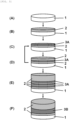
FIG. 3 shows a schematic view describing a flow of a method for manufacturing a silicon substrate for a quantum computer according to the present invention. - Hereinafter, the present invention will be described in detail. However, the present invention is not limited thereto.
- As described above, a silicon substrate for a quantum computer capable of suppressing the effect of 29Si to suppress the effect of a nuclear spin and a method for manufacturing such a substrate has been required.
- To solve the above problem, the present inventors have earnestly studied and found a method for manufacturing a silicon substrate for a quantum computer including the steps of forming a Si epitaxial layer by epitaxial growth using a Si source gas as a silicon-based raw material gas, in which a total content of 28Si and 30Si in a whole silicon contained in the silicon-based raw material gas is 99.9% or more, on a silicon substrate, forming an oxygen (O) δ-doped layer by oxidizing a surface of the Si epitaxial layer, and forming a Si epitaxial layer by epitaxial growth using a Si source gas, in which a total content of 28Si and 30Si in a whole silicon contained in the silicon-based raw material gas is 99.9% or more, on the δ-doped layer. Through this method, the silicon substrate for a quantum computer capable of suppressing an effect of a nuclear spin can be manufactured, and a silicon substrate, in which an isotope effect suitable for a quantum computer can be fully demonstrated and a single-electron transistor can be easily formed, can be manufactured. Based on this finding, the present invention has been completed.
- In addition, the present inventors have found a method for manufacturing a silicon substrate for a quantum computer including the steps of forming a 28Si epitaxial layer by epitaxial growth using a 28Si source gas as a silicon-based raw material gas on a silicon substrate, forming an oxygen (O) δ-doped layer by oxidizing a surface of the 28Si epitaxial layer, and forming a 28Si epitaxial layer by epitaxial growth using a 28Si source gas on the δ-doped layer. Through this method, the silicon substrate for a quantum computer capable of suppressing an effect of a nuclear spin can be manufactured, and a silicon substrate, in which an isotope effect suitable for a quantum computer can be fully demonstrated, and a single-electron transistor can be easily formed, can be manufactured. Based on this finding, the present invention has been completed.
- In addition, the present inventors have earnestly studied the above problem and found a silicon substrate for a quantum computer including a silicon substrate, a Si epitaxial layer, being an epitaxial layer on the silicon substrate, having a composition with which a total content of 28Si and 30Si in a whole silicon of the epitaxial layer is 99.9% or more, a SiO2 layer, being a SiO2 layer on the Si epitaxial layer, having a composition in which a total content of 28Si and 30Si in a whole silicon of the SiO2 layer is 99.9% or more, and a Si epitaxial layer, being an epitaxial layer on the SiO2 layer, having a composition in which a total content of 28Si and 30Si in a whole silicon of the epitaxial layer is 99.9% or more. Through this substrate, the substrate can be the silicon substrate for a quantum computer capable of suppressing an effect of a nuclear spin, as well as the silicon substrate in which an isotope effect suitable for a quantum computer can be fully demonstrated and a single-electron transistor can be easily formed. Based on this finding, the present invention has been completed.
- In addition, the present inventors have found a silicon substrate for a quantum computer including a silicon substrate, a 28Si epitaxial layer on the silicon substrate, a 28SiO2 layer on the 28Si epitaxial layer, and a 28Si epitaxial layer on the 28SiO2 layer. Through this substrate, the substrate can be the silicon substrate for a quantum computer capable of suppressing an effect of a nuclear spin, as well as the silicon substrate in which an isotope effect suitable for a quantum computer can be fully demonstrated and a single-electron transistor can be easily formed. Based on this finding, the present invention has been completed.
- Hereinafter, the description will be given, referring to the drawings.
- Hereinafter, the term "28Si" is used as an example to describe a definition of terms; however, the same expressions may be used for other isotopes (such as 30Si).
- In the present description, "28Si source gas", being the silicon-based raw material gas, indicates a gas that has a composition in which a content of 28Si in a whole silicon in a silicon-containing gas is 99.9% or more. "28Si monosilane gas" (may also be expressed as "28SiH4") indicates a monosilane gas that has a composition in which a content of 28Si in a whole silicon in the monosilane (SiH4) gas is 99.9% or more. The silicon has three stable isotopes, i.e., 28Si, 29Si, 30Si. Although a natural abundance thereof is 92.23%, 4.67%, and 3.1%, respectively, for example, the 28Si source gas can be produced by centrifugation of the silicon-containing gas (silane-based gas) composed of natural Si isotope composition. The 30Si source gas or "the Si source gas having the total content of 28Si and 30Si in a whole silicon contained in the silicon-based raw material gas is 99.9% or more" can also be produced in the same manner.
- In the present description, the "28Si epitaxial layer" indicates an epitaxial layer that has a composition in which a content of 28Si in a whole silicon in the epitaxial layer is 99.9% or more. For example, this layer can be obtained by epitaxial growth using the 28Si source gas.
- In the present description, "28SiO2" indicates SiO2 that has a composition in which a content of 28Si in a whole silicon in SiO2 is 99.9% or more. For example, this can be obtained by oxidizing the 28Si epitaxial layer.
- In the present description, "δ-doped layer" is a layer in which an element different from a base material is introduced therein at a level of approximately a single atomic layer. An oxygen (O) δ-doped layer includes, for example, a case where oxygen of less than the single atomic layer (1.36×10¹⁵ atoms/cm2) is introduced on the silicon substrate. Note that the δ-doping method includes methods such as a method disclosed in
Patent Document 2. - The present inventors have earnestly studied the above problem and, as a result, found a silicon substrate for a quantum computer including a silicon substrate, a Si epitaxial layer, being an epitaxial layer on the silicon substrate, having a composition in which a total content of 28Si and 30Si in a whole silicon in the epitaxial layer is 99.9% or more, a SiO2 layer, being a SiO2 layer on the Si epitaxial layer, having a composition in which a total content of 28Si and 30Si in a whole silicon in the SiO2 layer is 99.9% or more, and a Si epitaxial layer, being an epitaxial layer on the SiO2 layer, having a composition in which a total content of 28Si and 30Si in a whole silicon in the epitaxial layer is 99.9% or more. Through this, it is found such a substrate can be the silicon substrate for a quantum computer being capable of suppressing the effect of 29Si, thereby suppressing the effect of a nuclear spin.
- The Si epitaxial layer in the inventive silicon substrate for a quantum computer only needs to have a composition in which a total content of 28Si and 30Si is 99.9% or more in the whole silicon contained in the epitaxial layer, and is not necessarily required to contain both 28Si and 30Si. The case in which the content of 28Si in a whole silicon in the epitaxial layer is 99.9% or more, or a case where the content of 30Si is 99.9% or more may be sufficient.
- In this case, the SiO2 layer is preferably the oxygen (O) δ-doped layer. Such a silicon substrate for a quantum computer serves as a silicon substrate having the δ-doped layer suitable for a quantum computer.
- Moreover, the SiO2 layer is preferably a buried oxide film (BOX) layer in an SOI structure. Such a silicon substrate for a quantum computer serves as a silicon substrate having the SOI structure suitable for a quantum computer.
- Furthermore, the above silicon substrate for a quantum computer is preferably provided with a device thereon. Such a semiconductor apparatus serves as a semiconductor apparatus where the effect of the nuclear spin is suppressed.
- Regarding more detailed embodiment, the description will be given in the following second embodiment which corresponds to the silicon substrate for a quantum computer according to the first embodiment in which the composition of the content of 28Si in the whole silicon in the epitaxial layer is set to 99.9% or more.
- In addition, the present inventors found a silicon substrate for a quantum computer including a silicon substrate, a 28Si epitaxial layer on the silicon substrate, a 28SiO2 layer on the 28Si epitaxial layer, and a 28Si epitaxial layer on the 28SiO2 layer, and this silicon substrate can suppress an effect of 29Si and thus an effect of a nuclear spin. As described above, the silicon substrate for a quantum computer according to the second embodiment of the present invention corresponds to the silicon substrate for a quantum computer, according to the above first embodiment, in which a composition of a content of 28Si in a whole silicon in an epitaxial layer is set to 99.9% or more.
-
FIG. 1 shows an example of a structure of the inventive silicon substrate for a quantum computer. The silicon substrate for a quantum computer according to the second embodiment includes asilicon substrate 1, a 28Si epitaxial layer 2 on thesilicon substrate 1, a 28SiO2 layer 3 on the 28Si epitaxial layer 2, and the 28Si epitaxial layer 2 on the 28SiO2 layer 3. - The 28SiO2 layer 3 in the silicon substrate for a quantum computer shown in
FIG. 1 can be an oxygen (O) δ-doped layer.FIG. 2 shows an example in which a plurality of layers of oxygen (O) δ-doped layers 3A (a plurality of pairs of the oxygen (O) δ-doped layers 3A and adjacent the 28Si epitaxial layers 2), but the oxygen (O) δ-doped layer may be single layer (one layer) as in the 28SiO2 layer 3 inFIG. 1 . - Moreover, the 28SiO2 layer 3 in the silicon substrate for a quantum computer shown in
FIG. 1 can be a buried oxide film (BOX) layer in an SOI structure. In this case, the buried oxide film (BOX) layer (28SiO2 layer) can have a film thickness of approximately 0.01 to 1 µm. - The
silicon substrate 1 used for the inventive silicon substrate for a quantum computer will be described. Thesilicon substrate 1 is not particularly limited as long as the 28Si epitaxial layer can be deposited on this substrate. A diameter, thickness, dopant, etc., are not particularly limited. In the quantum computer, a microwave and the like are used to read out a spin state of electrons, etc., which exhibit quantized behavior. Consequently, a high-resistance substrate is preferably used to reduce signal distortion in a transmission path. In particular, the substrate having a resistivity of about 1000 Ω·cm or higher is preferable. This enables the silicon substrate for a quantum computer to stably extract undistorted signal obtained through spin resonance. The upper limit of the resistivity of the silicon substrate is not particularly limited but can, for example, be 100000 Ω·cm or lower. - A semiconductor apparatus having a device provided on the inventive silicon substrate for a quantum computer described above becomes the semiconductor apparatus in which the effect of the nuclear spin is suppressed.
- Next, a method for manufacturing a silicon substrate for a quantum computer, which is the third embodiment of the present invention, will be described. The inventive method for manufacturing a silicon substrate for a quantum computer includes the steps of forming a Si epitaxial layer by epitaxial growth using a Si source gas as a silicon-based raw material gas, in which a total content of 28Si and 30Si in a whole silicon contained in the silicon-based raw material gas is 99.9% or more, on a silicon substrate, forming an oxygen (O) δ-doped layer by oxidizing a surface of the Si epitaxial layer, and forming a Si epitaxial layer by epitaxial growth using a Si source gas, in which a total content of 28Si and 30Si in a whole silicon contained in the silicon-based raw material gas is 99.9% or more, on the δ-doped layer.
- In a method for manufacturing a silicon substrate for a quantum computer according to the third embodiment of the present invention, the Si source gas in which a total content of 28Si and 30Si in a whole silicon contained in a silicon-based raw material gas is 99.9% or more is sufficient as a silicon-based raw material gas, not necessarily required to contain both 28Si and 30Si. This includes a case where the content of 28Si in a whole silicon contained in a silicon-based raw material gas is 99.9% or more, or a case where the content of 30Si is 99.9% or more.
- A monosilane gas is preferably used as the Si source gas. This enables the manufacture of the silicon substrate suitable for a quantum computer at a lower temperature.
- It is preferred that the step of forming the oxygen (O) δ-doped layer and the step of forming the Si epitaxial layer on the δ-doped layer are repeated to form a plurality of pairs of the δ-doped layers, and the Si epitaxial layers on the δ-doped layers. This enables the manufacture of the silicon substrate to be more suitable for a quantum computer.
- Moreover, it is preferred that a Si epitaxial layer of an outermost surface of the silicon substrate for a quantum computer has a thickness greater than that of a Si epitaxial layer other than the Si epitaxial layer of the outermost surface layer. This enables the manufacture of the silicon substrate that is further suitable for a quantum computer.
- In this case, the silicon substrate is preferred to have a resistivity of 1000 Ω·cm or higher. This enables the manufacture of the silicon substrate for a quantum computer capable of stably extracting undistorted signals obtained through spin resonance. The upper limit of the resistivity of the silicon substrate is not particularly limited but can, for example, be 100000 Ω·cm or lower.
- Regarding more detailed embodiment, the description will be given in the following fourth embodiment which corresponds to the method for manufacturing the silicon substrate for a quantum computer according to the third embodiment in which the composition of the content of 28Si in the whole silicon contained in a silicon-based raw material gas is set to 99.9% or more.
- Moreover, a method for manufacturing a silicon substrate for a quantum computer according to the fourth embodiment of the present invention includes the steps of forming a 28Si epitaxial layer by epitaxial growth using a 28Si source gas as a silicon-based raw material gas on a silicon substrate, forming an oxygen (O) δ-doped layer by oxidizing a surface of the 28Si epitaxial layer, and forming a 28Si epitaxial layer by epitaxial growth using the 28Si source gas on the δ-doped layer. As described above, the method for manufacturing the silicon substrate for a quantum computer according to the fourth embodiment of the present invention corresponds to the method for the silicon substrate for a quantum computer according to the above third embodiment in which a composition of content of 28Si in a whole silicon contained in a silicon-based raw material gas is set to 99.9% or more. Hereinafter, the description will be given in detail.
- First, a
silicon substrate 1 is provided as shown inFIG. 3(A) . - Next, as shown in
FIG. 3(B) , thesilicon substrate 1 is epitaxially grown (deposited) to form a 28Si epitaxial layer 2. In this case, a CVD method can form the epitaxial layer with better crystallinity. In the epitaxial growth, for example, the 28Si source gas obtained by isotopic enrichment is used as the silicon-based raw material gas. As the 28Si source gas, it is particularly preferable to use a 28Si monosilane gas (28SiH4). This enables epitaxial growth to be performed at a lower temperature. - Moreover, a thickness of the 28
Si epitaxial layer 2 at this time is not particularly limited, but a thickness having about 0.01 to 1 µm is sufficient. As clear from an example such as NMR of Si, this is reasonable when considering that an interaction between an electron spin and a nuclear spin, which is the strongest between adjacent atoms, and an effect thereof is diminished as separating the atoms by a few atoms. - Then as shown in
FIG. 3(C) , a 28SiO2 layer which is an oxide film for electron confinement is formed. In an example ofFIG. 3 , an oxygen (O) δ-dopedlayer 3A is formed using an oxygen (O) δ-doped method. - By using the δ-doped method to oxidize a surface of the 28Si epitaxial layer and then form the oxygen (O) δ-doped
layer 3A, it becomes possible to convert the silicon which is an insulating film into silicon oxide (28SiO2) which is unaffected from the nuclear spin, thereby avoiding the effect of the interaction between the electron spin and the nuclear spin. - Next, as shown in
FIG. 3(D) , the 28Si epitaxial layer 2 is deposited on this δ-doped layer. As in a case of the 28Si epitaxial layer 2 at the first layer, as described above, the CVD method can form the epitaxial layer with better crystallinity. The 28Si source gas such as isotopically enriched 28SiH4 is used as a raw material gas. Moreover, a thickness of the epitaxial layer at this time is not required to be as thick as that of the 28Si epitaxial layer 2 at the first layer and can be adjusted as appropriate to enable electron confinement. For example, the thickness thereof can be about 0.001 to 0.5 µm. - Although a device can be produced using a structure as is, the insulation layer formed up to this step is, as referred to as δ-doped, only oxygen inserted at an atomic level, and thus the insulation thereof may not be sufficient. Therefore, it is also preferable to repeat the step for forming the oxygen (O) δ-doped
layer 3A inFIG. 3(C) and the step of forming the 28Si epitaxial layer 2 on the δ-doped layer inFIG. 3(D) to form a plurality of pairs of the oxygen (O) δ-doped layers 3A and the 28Si epitaxial layers on the δ-doped layers as shown inFIG. 3(E) . This makes the silicon substrate more suitable for a quantum computer. - As shown in
FIG. 3(F) , it is also possible to oxidize and integrate a plurality of δ-doped layers by subsequent heat treatment, thereby forming a thick insulation layer. The resulting thick insulation layer can form an SOI structure that can function as a buried oxide film (BOX)layer 3B. This makes the silicon substrate more suitable for a quantum computer. - The number of stacks of the oxygen (O) δ-
doped layers 3A and the 28Si epitaxial layers 2 on the δ-doped layers can be adjusted as appropriate according to the characteristics and design of the device. Moreover, when integrating a plurality of δ-doped layers by oxidation, it is preferable to make the thickness of the 28Si epitaxial layer 2 of an outermost layer greater than the thickness of the 28Si epitaxial layer other than the 28Si epitaxial layer of the outermost layer. For example, the thickness can be about 0.002 to 1 µm. In this way, even when the oxidation is performed, the 28Si epitaxial layer 2 of the outermost layer is not eliminated. - By using the 28Si-rich silicon layer (28Si epitaxial layer), the 28Si-rich oxide film (28SiO2 layer) can also be formed in the insulation layer.
- Hereinafter, the present invention will be specifically described with reference to Example. However, the present invention is not limited thereto.
- A boron-doped silicon substrate having a diameter of 300 mm (resistivity: 1000 Ω·cm) was provided, 28SiH4 (isotope 99.94%) was used as a raw material, and a silicon epitaxial growth was performed. The film was grown to a thickness of 1 µm under reduced pressure condition of 100 Torr (13332 Pa) at a temperature of 850°C. Subsequently, a 2-hour left-in-atmosphere was performed to form a native oxide film composed of 28SiO2 (oxygen δ-doping), and a silicon epitaxial layer was formed again to a thickness of 3 nm, using 28SiH4 (isotope 99.94%) as the raw material, under reduced pressure condition of 100 Torr (13332 Pa) at the temperature of 850°C. Furthermore, a 2-hour left-in-atmosphere was performed to form the native oxide film composed of 28SiO2 (oxygen δ-doping). Thereafter, the formations of the silicon epitaxial layers to a thickness of 3 nm were repeated four times, using 28SiH4 (isotope 99.94%) as the raw material, under reduced pressure condition of 100 Torr (13332 Pa) at the temperature of 850°C. Finally, the silicon epitaxial layer was formed to a thickness of 100 nm, using 28SiH4 (isotope 99.94%) as the raw material, under reduced pressure condition of 100 Torr (13332 Pa) at the temperature of 850°C. Heat treatment was then performed at 800°C for 10 minutes, oxidizing the oxygen δ-doped layer to form a single oxide film (buried oxide film (BOX) layer), and then an SOI substrate having the 28Si epitaxial layer as a top layer was produced.
- As described above, according to Example of the present invention, the silicon substrate was successfully obtained in which the substrate was the silicon substrate for a quantum computer capable of suppressing an effect of a nuclear spin, as well as the silicon substrate in which an isotope effect suitable for a quantum computer was fully demonstrated and a single-electron transistor was easily formed.
- The present description includes the following embodiments.
- [A]: A method for manufacturing a silicon substrate for a quantum computer, the method comprising the steps of:
- forming a Si epitaxial layer by epitaxial growth using a Si source gas as a silicon-based raw material gas, in which a total content of 28Si and 30Si in a whole silicon contained in the silicon-based raw material gas is 99.9% or more, on a silicon substrate;
- forming an oxygen (O) δ-doped layer by oxidizing a surface of the Si epitaxial layer; and
- forming a Si epitaxial layer by epitaxial growth using a Si source gas, in which a total content of 28Si and 30Si in a whole silicon contained in the silicon-based raw material gas is 99.9% or more, on the δ-doped layer.
- [B]: The method for manufacturing a silicon substrate for a quantum computer according to the above [A], wherein
a monosilane gas is used as the Si source gas. - [C]: The method for manufacturing a silicon substrate for a quantum computer according to the above [A] or [B], wherein
the step of forming the oxygen (O) δ-doped layer and the step of forming the Si epitaxial layer on the δ-doped layer are repeated to form a plurality of pairs of the δ-doped layers, and the Si epitaxial layers on the δ-doped layers. - [D]: The method for manufacturing a silicon substrate for a quantum computer according to the above [C], wherein
a Si epitaxial layer of an outermost surface of the silicon substrate for a quantum computer has a thickness greater than that of a Si epitaxial layer other than the Si epitaxial layer of the outermost surface layer. - [E]: The method for manufacturing a silicon substrate for a quantum computer according to the above [D], wherein
a plurality of the δ-doped layers is integrated to produce an SOI structure by heat-treating the silicon substrate for a quantum computer.- [1]: A method for manufacturing a silicon substrate for a quantum computer, the method comprising the steps of:
- forming a 28Si epitaxial layer by epitaxial growth using a 28Si source gas as a silicon-based raw material gas on a silicon substrate;
- forming an oxygen (O) δ-doped layer by oxidizing a surface of the 28Si epitaxial layer; and
- forming a 28Si epitaxial layer by epitaxial growth using a 28Si source gas on the δ-doped layer.
- [2]: The method for manufacturing a silicon substrate for a quantum computer according to the above [1], wherein
a 28Si monosilane gas is used as the 28Si source gas. - [3]: The method for manufacturing a silicon substrate for a quantum computer according to the above [1] or [2], wherein
the step of forming the oxygen (O) δ-doped layer and the step of forming the 28Si epitaxial layer on the δ-doped layer are repeated to form a plurality of pairs of the δ-doped layers, and the 28Si epitaxial layers on the δ-doped layers. - [4]: The method for manufacturing a silicon substrate for a quantum computer according to the above [3], wherein
a 28Si epitaxial layer of an outermost surface of the silicon substrate for a quantum computer has a thickness greater than that of a 28Si epitaxial layer other than the 28Si epitaxial layer of the outermost surface. - [5]: The method for manufacturing a silicon substrate for a quantum computer according to the above [4], wherein
a plurality of the δ-doped layers is integrated to produce an SOI structure by heat-treating the silicon substrate for a quantum computer. - [6]: The method for manufacturing a silicon substrate for a quantum computer according to the above [A], [B], [C], [D], [E], [1], [2], [3], [4], or [5], wherein
the silicon substrate has a resistivity of 1000 Ω·cm or higher.
- [1]: A method for manufacturing a silicon substrate for a quantum computer, the method comprising the steps of:
- [F]: A silicon substrate for a quantum computer comprising:
- a silicon substrate;
- a Si epitaxial layer, being an epitaxial layer on the silicon substrate, having a composition in which a total content of 28Si and 30Si in a whole silicon of the epitaxial layer is 99.9% or more;
- a SiO2 layer, being a SiO2 layer on the Si epitaxial layer, having a composition in which a total content of 28Si and 30Si in a whole silicon of the SiO2 layer is 99.9% or more; and
- a Si epitaxial layer, being an epitaxial layer on the SiO2 layer, having a composition in which a total content of 28Si and 30Si in a whole silicon of the epitaxial layer is 99.9% or more.
- [G]: The silicon substrate for a quantum computer according to the above [F], wherein
the SiO2 layer is an oxygen (O) δ-doped layer. - [H]: The silicon substrate for a quantum computer according to the above [F], wherein
the SiO2 layer is a buried oxide film (BOX) layer in an SOI structure.- [7]: A silicon substrate for a quantum computer comprising:
- a silicon substrate;
- a 28Si epitaxial layer on the silicon substrate;
- a 28SiO2 layer on the 28Si epitaxial layer; and
- a 28Si epitaxial layer on the 28SiO2 layer.
- [8]: The silicon substrate for a quantum computer according to the above [7], wherein
the 28SiO2 layer is an oxygen (O) δ-doped layer. - [9]: The silicon substrate for a quantum computer according to the above [7], wherein
the 28SiO2 layer is a buried oxide film (BOX) layer in an SOI structure. - [10]: A semiconductor apparatus comprising a device on a silicon substrate, the substrate being for a quantum computer according to the above [F], [G], [H], [7], [8], or [9].
- [7]: A silicon substrate for a quantum computer comprising:
- It should be noted that the present invention is not limited to the above-described embodiments. The embodiments are just examples, and any examples that have substantially the same feature and demonstrate the same functions and effects as those in the technical concept disclosed in claims of the present invention are included in the technical scope of the present invention.
Claims (18)
- A method for manufacturing a silicon substrate for a quantum computer, the method comprising the steps of:forming a Si epitaxial layer by epitaxial growth using a Si source gas as a silicon-based raw material gas, in which a total content of 28Si and 30Si in a whole silicon contained in the silicon-based raw material gas is 99.9% or more, on a silicon substrate;forming an oxygen (O) δ-doped layer by oxidizing a surface of the Si epitaxial layer; andforming a Si epitaxial layer by epitaxial growth using a Si source gas, in which a total content of 28Si and 30Si in a whole silicon contained in the silicon-based raw material gas is 99.9% or more, on the δ-doped layer.
- The method for manufacturing a silicon substrate for a quantum computer according to claim 1, wherein
a monosilane gas is used as the Si source gas. - The method for manufacturing a silicon substrate for a quantum computer according to claim 1, wherein
the step of forming the oxygen (O) δ-doped layer and the step of forming the Si epitaxial layer on the δ-doped layer are repeated to form a plurality of pairs of the δ-doped layers, and the Si epitaxial layers on the δ-doped layers. - The method for manufacturing a silicon substrate for a quantum computer according to claim 3, wherein
a Si epitaxial layer of an outermost surface of the silicon substrate for a quantum computer has a thickness greater than that of a Si epitaxial layer other than the Si epitaxial layer of the outermost surface layer. - The method for manufacturing a silicon substrate for a quantum computer according to claim 4, wherein
a plurality of the δ-doped layers is integrated to produce an SOI structure by heat-treating the silicon substrate for a quantum computer. - A method for manufacturing a silicon substrate for a quantum computer, the method comprising the steps of:forming a 28Si epitaxial layer by epitaxial growth using a 28Si source gas as a silicon-based raw material gas on a silicon substrate;forming an oxygen (O) δ-doped layer by oxidizing a surface of the 28Si epitaxial layer; andforming a 28Si epitaxial layer by epitaxial growth using a 28Si source gas on the δ-doped layer.
- The method for manufacturing a silicon substrate for a quantum computer according to claim 6, wherein
a 28Si monosilane gas is used as the 28Si source gas. - The method for manufacturing a silicon substrate for a quantum computer according to claim 6, wherein
the step of forming the oxygen (O) δ-doped layer and the step of forming the 28Si epitaxial layer on the δ-doped layer are repeated to form a plurality of pairs of the δ-doped layers, and the 28Si epitaxial layers on the δ-doped layers. - The method for manufacturing a silicon substrate for a quantum computer according to claim 8, wherein
a 28Si epitaxial layer of an outermost surface of the silicon substrate for a quantum computer has a thickness greater than that of a 28Si epitaxial layer other than the 28Si epitaxial layer of the outermost surface. - The method for manufacturing a silicon substrate for a quantum computer according to claim 9, wherein
a plurality of the δ-doped layers is integrated to produce an SOI structure by heat-treating the silicon substrate for a quantum computer. - The method for manufacturing a silicon substrate for a quantum computer according to any one of claims 1 to 10, wherein
the silicon substrate has a resistivity of 1000 Ω·cm or higher. - A silicon substrate for a quantum computer comprising:a silicon substrate;a Si epitaxial layer, being an epitaxial layer on the silicon substrate, having a composition in which a total content of 28Si and 30Si in a whole silicon of the epitaxial layer is 99.9% or more;a SiO2 layer, being a SiO2 layer on the Si epitaxial layer, having a composition in which a total content of 28Si and 30Si in a whole silicon of the SiO2 layer is 99.9% or more; anda Si epitaxial layer, being an epitaxial layer on the SiO2 layer, having a composition in which a total content of 28Si and 30Si in a whole silicon of the epitaxial layer is 99.9% or more.
- The silicon substrate for a quantum computer according to claim 12, wherein
the SiO2 layer is an oxygen (O) δ-doped layer. - The silicon substrate for a quantum computer according to claim 12, wherein
the SiO2 layer is a buried oxide film (BOX) layer in an SOI structure. - A silicon substrate for a quantum computer comprising:a silicon substrate;a 28Si epitaxial layer on the silicon substrate;a 28SiO2 layer on the 28Si epitaxial layer; anda 28Si epitaxial layer on the 28SiO2 layer.
- The silicon substrate for a quantum computer according to claim 15, wherein
the 28SiO2 layer is an oxygen (O) δ-doped layer. - The silicon substrate for a quantum computer according to claim 15, wherein
the 28SiO2 layer is a buried oxide film (BOX) layer in an SOI structure. - A semiconductor apparatus comprising a device on a silicon substrate, the substrate being for a quantum computer according to any one of claims 12 to 17.
Applications Claiming Priority (3)
| Application Number | Priority Date | Filing Date | Title |
|---|---|---|---|
| JP2022126471 | 2022-08-08 | ||
| JP2022141365A JP7718359B2 (en) | 2022-08-08 | 2022-09-06 | Manufacturing method of silicon substrate for quantum computer, silicon substrate for quantum computer and semiconductor device |
| PCT/JP2023/027757 WO2024034433A1 (en) | 2022-08-08 | 2023-07-28 | Method for producing silicon substrate for quantum computers, silicon substrate for quantum computers, and semiconductor device |
Publications (1)
| Publication Number | Publication Date |
|---|---|
| EP4571815A1 true EP4571815A1 (en) | 2025-06-18 |
Family
ID=89851549
Family Applications (1)
| Application Number | Title | Priority Date | Filing Date |
|---|---|---|---|
| EP23852406.0A Pending EP4571815A1 (en) | 2022-08-08 | 2023-07-28 | Method for producing silicon substrate for quantum computers, silicon substrate for quantum computers, and semiconductor device |
Country Status (6)
| Country | Link |
|---|---|
| US (1) | US20260047406A1 (en) |
| EP (1) | EP4571815A1 (en) |
| KR (1) | KR20250048241A (en) |
| CN (1) | CN119654700A (en) |
| TW (1) | TW202418369A (en) |
| WO (1) | WO2024034433A1 (en) |
Family Cites Families (10)
| Publication number | Priority date | Publication date | Assignee | Title |
|---|---|---|---|---|
| JPH0846222A (en) * | 1994-05-31 | 1996-02-16 | Texas Instr Inc <Ti> | Injection silicon resonance tunneling diode and method of manufacturing the same |
| JP2004039735A (en) * | 2002-07-01 | 2004-02-05 | Fujitsu Ltd | Semiconductor substrate and method of manufacturing the same |
| JP4845375B2 (en) * | 2004-12-14 | 2011-12-28 | 富士通株式会社 | Quantum device, control method thereof, and manufacturing method thereof |
| JP2008277477A (en) * | 2007-04-27 | 2008-11-13 | Fujitsu Microelectronics Ltd | Semiconductor substrate and manufacturing method thereof |
| US9558939B1 (en) * | 2016-01-15 | 2017-01-31 | Atomera Incorporated | Methods for making a semiconductor device including atomic layer structures using N2O as an oxygen source |
| US10418781B1 (en) * | 2018-07-06 | 2019-09-17 | Ii-Vi Delaware, Inc. | Quantum well passivation structure for laser facets |
| JP7247902B2 (en) | 2020-01-10 | 2023-03-29 | 信越半導体株式会社 | Epitaxial wafer manufacturing method |
| US11837634B2 (en) * | 2020-07-02 | 2023-12-05 | Atomera Incorporated | Semiconductor device including superlattice with oxygen and carbon monolayers |
| JP7347350B2 (en) * | 2020-07-10 | 2023-09-20 | 信越半導体株式会社 | Method for setting epitaxial growth conditions and method for manufacturing epitaxial wafers |
| JP7322832B2 (en) | 2020-07-29 | 2023-08-08 | 信越半導体株式会社 | Manufacturing method of semiconductor device for quantum computer |
-
2023
- 2023-07-28 CN CN202380056352.6A patent/CN119654700A/en active Pending
- 2023-07-28 US US18/998,666 patent/US20260047406A1/en active Pending
- 2023-07-28 WO PCT/JP2023/027757 patent/WO2024034433A1/en not_active Ceased
- 2023-07-28 KR KR1020257003470A patent/KR20250048241A/en active Pending
- 2023-07-28 EP EP23852406.0A patent/EP4571815A1/en active Pending
- 2023-08-02 TW TW112128945A patent/TW202418369A/en unknown
Also Published As
| Publication number | Publication date |
|---|---|
| WO2024034433A1 (en) | 2024-02-15 |
| KR20250048241A (en) | 2025-04-08 |
| CN119654700A (en) | 2025-03-18 |
| US20260047406A1 (en) | 2026-02-12 |
| TW202418369A (en) | 2024-05-01 |
Similar Documents
| Publication | Publication Date | Title |
|---|---|---|
| JP4238087B2 (en) | Method for producing SiGe on insulator substrate material | |
| JP3058954B2 (en) | Method of manufacturing semiconductor device having growth layer on insulating layer | |
| Johannes Luyken et al. | Growth and electronic properties of self-organized quantum rings | |
| US6800518B2 (en) | Formation of patterned silicon-on-insulator (SOI)/silicon-on-nothing (SON) composite structure by porous Si engineering | |
| JP2007194336A (en) | Manufacturing method of semiconductor wafer | |
| JP4954853B2 (en) | Crystal defect and / or stress field manifestation process at the molecular adhesion interface of two solid materials | |
| US9620615B2 (en) | IGBT manufacturing method | |
| JP2007335867A (en) | Method for limiting vacancy diffusion in heterostructures | |
| US20080277690A1 (en) | STRAINED SILICON-ON-INSULATOR BY ANODIZATION OF A BURIED p+ SILICON GERMANIUM LAYER | |
| CN105340074B (en) | SOI substrate preparation method and SOI substrate | |
| JP2701902B2 (en) | Semiconductor structure having porous strained layer and method of manufacturing SOI semiconductor structure | |
| Bolkhovityanov et al. | Artificial GeSi substrates for heteroepitaxy: Achievements and problems | |
| Khan et al. | Multiterminal quantized conductance in InSb nanocrosses | |
| US20260047406A1 (en) | Method for manufacturing silicon substrate for quantum computer, silicon substrate for quantum computer, and semiconductor apparatus | |
| JP2989051B2 (en) | Silicon carbide bipolar semiconductor device and method of manufacturing the same | |
| JP2024023112A (en) | Method for manufacturing silicon substrate for quantum computer, silicon substrate for quantum computer and semiconductor device | |
| CN112802961A (en) | Method for preparing InSb functional layer | |
| CN114530497B (en) | Enhancement method of hole linear Rashba spin orbit coupling effect | |
| CN118966375B (en) | A quantum bit and preparation method thereof, and quantum chip | |
| Liu et al. | A novel thin buffer concept for epitaxial growth of relaxed SiGe layers with low threading dislocation density | |
| US6583451B2 (en) | Process for fabricating a network of nanometric lines made of single-crystal silicon and device obtained | |
| Fahrner | Contributions of Oxygen, Silicon, and Hydrogen to the Interface States of an Si‐SiO2, Interface | |
| Kikuchi et al. | Solid-source doping by using phosphosilicate glass into p-type bulk Si (100) substrate: Role of the capping SiO2 barrier | |
| EP4618720A1 (en) | Structures including an isotopically-depleted semiconductor layer | |
| JPS6060716A (en) | Manufacture of semiconductor substrate |
Legal Events
| Date | Code | Title | Description |
|---|---|---|---|
| STAA | Information on the status of an ep patent application or granted ep patent |
Free format text: STATUS: THE INTERNATIONAL PUBLICATION HAS BEEN MADE |
|
| PUAI | Public reference made under article 153(3) epc to a published international application that has entered the european phase |
Free format text: ORIGINAL CODE: 0009012 |
|
| STAA | Information on the status of an ep patent application or granted ep patent |
Free format text: STATUS: REQUEST FOR EXAMINATION WAS MADE |
|
| 17P | Request for examination filed |
Effective date: 20250203 |
|
| AK | Designated contracting states |
Kind code of ref document: A1 Designated state(s): AL AT BE BG CH CY CZ DE DK EE ES FI FR GB GR HR HU IE IS IT LI LT LU LV MC ME MK MT NL NO PL PT RO RS SE SI SK SM TR |
|
| DAV | Request for validation of the european patent (deleted) | ||
| DAX | Request for extension of the european patent (deleted) |