EP4571574A1 - Rf communications device with emi reduction - Google Patents
Rf communications device with emi reduction Download PDFInfo
- Publication number
- EP4571574A1 EP4571574A1 EP23216838.5A EP23216838A EP4571574A1 EP 4571574 A1 EP4571574 A1 EP 4571574A1 EP 23216838 A EP23216838 A EP 23216838A EP 4571574 A1 EP4571574 A1 EP 4571574A1
- Authority
- EP
- European Patent Office
- Prior art keywords
- current
- communications device
- rectifier
- gain controller
- operable
- Prior art date
- Legal status (The legal status is an assumption and is not a legal conclusion. Google has not performed a legal analysis and makes no representation as to the accuracy of the status listed.)
- Pending
Links
Images


Classifications
-
- G—PHYSICS
- G06—COMPUTING OR CALCULATING; COUNTING
- G06K—GRAPHICAL DATA READING; PRESENTATION OF DATA; RECORD CARRIERS; HANDLING RECORD CARRIERS
- G06K19/00—Record carriers for use with machines and with at least a part designed to carry digital markings
- G06K19/06—Record carriers for use with machines and with at least a part designed to carry digital markings characterised by the kind of the digital marking, e.g. shape, nature, code
- G06K19/067—Record carriers with conductive marks, printed circuits or semiconductor circuit elements, e.g. credit or identity cards also with resonating or responding marks without active components
- G06K19/07—Record carriers with conductive marks, printed circuits or semiconductor circuit elements, e.g. credit or identity cards also with resonating or responding marks without active components with integrated circuit chips
- G06K19/0701—Record carriers with conductive marks, printed circuits or semiconductor circuit elements, e.g. credit or identity cards also with resonating or responding marks without active components with integrated circuit chips at least one of the integrated circuit chips comprising an arrangement for power management
- G06K19/0715—Record carriers with conductive marks, printed circuits or semiconductor circuit elements, e.g. credit or identity cards also with resonating or responding marks without active components with integrated circuit chips at least one of the integrated circuit chips comprising an arrangement for power management the arrangement including means to regulate power transfer to the integrated circuit
-
- G—PHYSICS
- G06—COMPUTING OR CALCULATING; COUNTING
- G06K—GRAPHICAL DATA READING; PRESENTATION OF DATA; RECORD CARRIERS; HANDLING RECORD CARRIERS
- G06K19/00—Record carriers for use with machines and with at least a part designed to carry digital markings
- G06K19/06—Record carriers for use with machines and with at least a part designed to carry digital markings characterised by the kind of the digital marking, e.g. shape, nature, code
- G06K19/067—Record carriers with conductive marks, printed circuits or semiconductor circuit elements, e.g. credit or identity cards also with resonating or responding marks without active components
- G06K19/07—Record carriers with conductive marks, printed circuits or semiconductor circuit elements, e.g. credit or identity cards also with resonating or responding marks without active components with integrated circuit chips
- G06K19/0723—Record carriers with conductive marks, printed circuits or semiconductor circuit elements, e.g. credit or identity cards also with resonating or responding marks without active components with integrated circuit chips the record carrier comprising an arrangement for non-contact communication, e.g. wireless communication circuits on transponder cards, non-contact smart cards or RFIDs
Definitions
- This disclosure relates to an RF communications device and to an RFID tag comprising the RF communications device.
- Electromagnetic interference can inhibit the correct operation of RF communications devices such as RFID/NFC tags and active powered NFC controller ICs.
- the rectification of currents induced in an antenna of such a tag by a received electromagnetic signal can be problematic in this respect since the rectification process can itself produce unwanted emissions within the RF spectrum.
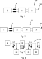
- Figure 1 shows a block diagram of a conventional RF communications device 100.
- Figure 1 shows the various components which are used for providing power for the RF communications device 100.
- the RF communications device 100 includes an antenna 2.
- the antenna 2 may be used for wireless communications to and from the RF communications device 100.
- a passive RF communications device 100 such as a Radio Frequency Identification (RFID) tag and/or a Near Field Communications (NFC) tag
- power for the RF communications device 100 may be derived from the incoming RF carrier wave (e.g., at 13.56MHz).
- the RF communications device 100 also includes antenna terminals 4, a rectifier 6 for rectifying the AC signal received at the antenna terminals into a DC voltage, and a limiter 8.
- the limiter 8 has an output 120, which provides a limited chip supply voltage V DDLIM for the RF communications device 100, which is derived from the rectified DC voltage that is outputted by the rectifier 6.
- the limiter 8 sinks current that is not used by the system to prevent the internal voltage exceeding the limits of the process technology which is used to manufacture the RF communications device 100.
- relatively high currents are required to pass through the rectifier 6, which is a non-linear component. As noted above, this can produce high levels of Electromagnetic Interference (EMI) which may violate ETSI limits and which interfere with the operation of the RF communications device 100 and/or other devices in the vicinity.
- EMI Electromagnetic Interference
- a Radio Frequency, RF, communications device comprising:
- Embodiments of this disclosure can modulate the current that is received from the antenna, thereby to reduce the amount of current that enters the rectifier.
- the reduced current in the rectifier can lead to a reduction in unwanted emissions (associated with the rectification process) within the RF spectrum.
- the voltage limiter may comprise a path for diverting a portion of the rectified current.
- the limited rectified voltage may be derived from (correspond to) a non-diverted remainder of the rectified current.
- the voltage limiter may be operable to produce a control signal according to a magnitude of the diverted portion of the rectified current.
- the control signal may be used to control the automatic gain controller.
- This feedback mechanism can allow the device to minimise the amount of current in the rectifier (further decreasing emissions in the RF spectrum) while optionally also retaining some slack (spare current) within the rectifier in case of increases in the demand for current by functional components of the RF communications device.
- the voltage limiter may include a circuit operable to compare the diverted portion of the rectified current with a reference current and to output the control signal as a digital signal indicative of the comparison.
- the RF communications device may further comprise a digital controller for controlling the automatic gain controller based at least in part on the control signal produced by the voltage limiter.
- the automatic gain controller may comprise a resistive digital-to-analogue-converter, RDAC.
- the digital controller may be operable to apply a digital control word to the RDAC to control a resistance of the RDAC.
- the digital controller may be operable to decrease the resistance of the RDAC in response to a determination that the control signal produced by voltage limiter is indicative of the diverted portion of the rectified current exceeding a predetermined maximum.
- the predetermined maximum may be set according to a highest tolerable current level within the rectifier.
- the tolerability of the current level within the rectifier may be determined according to the RF spectrum emissions associated with the rectification process at a given current level.
- the digital controller may be operable to increase the resistance of the RDAC in response to a determination that the control signal produced by the voltage limiter is indicative of the diverted portion of the rectified current falling beneath a predetermined minimum.
- the predetermined minimum may be set according to an anticipated increase in current drawn by the communications device. As noted above, this can allow the rectifier to retain a certain amount of current in reserve in case of increases in current demand by the functional components of the RF communications device.
- the automatic gain controller may be coupled in parallel across the pair of antenna terminals. This can allow a fully balanced operation of the circuit.
- the rectifier may comprise a full bridge rectifier comprising a plurality of diode-type devices (e.g. Schottky diodes or PMOS/NMOS transistors connected in diode configuration). Such a rectifier can reduce emissions in the RF spectrum compared to the traditional use of switched, non-linear, components.
- diode-type devices e.g. Schottky diodes or PMOS/NMOS transistors connected in diode configuration.
- the rectifier does not include any switched CMOS components.
- the RF communications device may further comprise a low pass filter coupled between the rectifier and the voltage limiter.
- a Radio Frequency Identification, RFID, tag or an active powered NFC controller IC comprising an RF communications device of the kind set out above.
- Radio Frequency refers to frequencies substantially equal to, or falling substantially within, the follow frequency values and bands: 120-150 kHz; 13.56 MHz; 433 MHz; 865-868 MHz; 902-928 MHz; 2450-5800 MHz; 3.1-10 GHz; 24.125 GHz.
- FIG. 2 shows a block diagram of an RF communications device 10 according to an embodiment of this disclosure.
- the RF communications device 10 includes a pair of antenna terminals 4.
- the antenna terminals may be connectable to an antenna 2.
- the RF communications device 10 is part of, or comprises, a Radio Frequency Identification (RFID) tag, a Near Field Communications (NFC) tag, or an active powered NFC controller IC.
- RFID Radio Frequency Identification
- NFC Near Field Communications
- the components of the RF communications device 10 shown in Figure 2 may be provided in a semiconductor die.
- the semiconductor die may be embedded in the tag (e.g. in the form of a smart card).
- the antenna 2 itself may be provided elsewhere in the tag. Accordingly, in some embodiments, the RF communications device 10 may be connectable to an antenna 2 using the terminals 4, whereas in other embodiments, the antenna 2 may also be considered to be part of the RF communications device 10.
- the RF communications device 10 in Figure 2 also includes an automatic gain controller (AGC) 12.
- AGC automatic gain controller
- the automatic gain controller 12 is coupled to the antenna terminals 4 for receiving an output current of the antenna 2, which is induced in the antenna by an incoming RF field (e.g., including a carrier at 13.56MHz).
- the automatic gain controller 12 is operable to convert the output current of the antenna 2 into a modulated current.
- the automatic gain controller 12 may be operable to apply a gain modulation to the AC signal received at the terminals 4.
- the automatic gain controller 12 comprises a controllable linear resistor.
- the automatic gain controller 12 may comprise a Resistive Digital to Analog Converter (RDAC).
- RDAC Resistive Digital to Analog Converter
- the RF communications device 10 in Figure 2 further includes a rectifier 16.
- the rectifier 16 is coupled to the automatic gain controller 12 to receive the modulated AC current produced by the automatic gain controller 12.
- the rectifier 16 is operable to convert the modulated current into a rectified current.
- the rectifier 16 may, in some embodiments, be optimized in a way that less non-linear components occur in the electromagnetic spectrum.
- the rectifier 16 may comprise a full bridge rectifier instead of a switched CMOS device.
- a full bridge rectifier can have reduced EMI emissions owing to its superior linearity compared to switched devices.
- the RF communications device 10 in Figure 2 also includes a voltage limiter 18.
- the voltage limiter 18 is coupled to the rectifier 16 for receiving the rectified current produced by the rectifier 16.
- the voltage limiter 18 is operable to convert the rectified current into a limited rectified voltage for supplying power to the RF communications device.
- the limiter 18 may have an output 20, which provides a limited chip supply voltage V DDLIM for the RF communications device 10, which is derived from the rectified DC voltage that is outputted by the rectifier 16.
- the automatic gain controller 12 can act as a primary limiter circuit that can remove at least some of the current that is induced via the antenna 2 (e.g., the current to be removed may be sunk into an Integrated Circuit (IC) in which the RF communications device 10 is comprised).
- the automatic gain controller 12 can sink current that is not required for the production of the limited chip supply voltage V DDLIM (e.g., in view of the presently prevailing current drawing requirements of a load coupled to the output 20) from the circuit shown in Figure 2 .
- the current that is passed to the rectifier 16 may be modulated for reducing the amplitude of the current to be rectified, which in turn can reduce EMI emissions by the rectifier 16.
- the voltage limiter 18 can further act to measure the remaining current, and this can be used to create feedback for controlling the modulation of the output current of the antenna 2 that is carried out by the automatic gain controller 12.
- Figure 3 shows a functional block diagram of an RF communications device 10 according to an embodiment of this disclosure.
- Figure 3 shows the automatic gain controller 12, rectifier 16, voltage limiter 18 described above in relation to Figure 2 .
- the antenna 2 is also shown.
- a load 30 is further shown in Figure 3 , which may be coupled to the output 20 described above in relation to Figure 2 .
- Figure 3 schematically shows the amounts of current flowing at/through the various components of the RF communications device 10 in two conditions, corresponding to whether a relatively small current A or a relatively large current E is currently being demanded by the load 30.
- the amount of current C that is provided to the rectifier 16 may be correspondingly small.
- the automatic gain controller 12 can sink a relatively large current B, whereby much of the current that is received from the antenna 2 does not reach the rectifier 16. In this way, the current demands of the load 30 may be satisfied in a way that reduces EMI emissions compared to devices of the kind described above in relation to Figure 1 .
- the amount of current D flowing in the voltage limiter 18 may be correspondingly small. This information may be used as feedback for the automatic gain controller 12.
- the amount of current G that is provided to the rectifier 16 may be correspondingly large.
- the automatic gain controller 12 can sink a relatively small current F. Accordingly, much of the current that is received from the antenna 2 reaches the rectifier 16. In this way, the current demands of the load 30 may be satisfied.
- the amount of EMI emissions produced by the rectifier 16 is inline line with the (presently) large current demand of the load 30.
- the rectified current that is outputted by the rectifier 16 is relatively large, the amount of current H flowing in the voltage limiter 18 may be correspondingly large. Again, this information may be used as feedback for the automatic gain controller 12.
- the currents B, F in the automatic gain controller 12 and their corresponding respective currents D, H in the voltage limiter 18 allow the function of current removal/limitation in the circuit to be shifted between the automatic gain controller 12 and the voltage limiter 18.
- B the current in the automatic gain controller 12
- D the current in the voltage limiter 18
- F the current in the voltage limiter 18
- E the available/induced current in the system, which may itself vary due to changes in the field strength received at the antenna 2.
- an "overhead” or “buffer” amount of current may be retained in the voltage limiter 18, over and above the prevailing current demands of the load 30. This can prevent situations in which the circuit is not able to satisfy short term increases in the current demands of the load 30.
- the “overhead” or “buffer” amount may be diverted from the load 30 by the voltage limiter 18 unless and until such fluctuations arise.
- embodiments of this disclosure can allow the amount of current supplied to the rectifier 16 to be "right sized” for the prevailing current demands of the load 30 (so as to reduce EMI emissions where the prevailing current demands permit it), while still allowing the current limiting function of the circuit to be performed by the voltage limiter 18 (e.g., so as to account for fluctuations in the current demands of the load 30).
- Figure 4 shows a circuit of an RF communications device 10 according to an embodiment of this disclosure.
- the circuit includes a pair of antenna terminals 4 of the kind already described above.
- a (low pass) filter capacitor 124 may be coupled across the antenna terminals 4.
- the automatic gain controller 12 is implemented using a Resistive Digital to Analog Converter (RDAC) as noted previously. It will be appreciated that other implementations for the automatic gain controller 12 are possible.
- RDAC Resistive Digital to Analog Converter
- the RDAC in this embodiment includes a variable resistance 122.
- the variable resistance 122 may be coupled across the antenna terminals 4 (e.g., in parallel with the optional filter capacitor 124).
- the variable resistance 122 may be controlled by a gain controller 200, which instructs 56 an RDAC controller 204 to set the resistance of the variable resistance 122 to a required level. It will be appreciated that increasing the resistance of the variable resistance 122, which is connected in parallel with the inputs of the rectifier 16, will increase the amount of current that passes from the antenna terminals 4 to the rectifier 16 (to be described below), and that conversely, the amount of current that passes from the antenna terminals 4 to the rectifier 16 may be decreased by lowering the resistance of the variable resistance 122.
- variable resistance is set according to a combination of the field strength of the signal received by the antenna 2 and the prevailing current demand of the load.
- variable resistance 122 may comprise a plurality of resistors coupled to the RDAC controller 204, with the resistors being enabled/disabled by one of more bits of a control word applied to the variable resistance 122 by the RDAC controller 204, under the guidance of the gain controller 200.
- the instruction 56 provided to the RDAC controller 204 by the gain controller 200 may also comprise a digital control word.
- the gain controller 200 may also directly monitor the operation of the variable resistance 122 (e.g., to verify the present resistance level), as illustrated by the signal 58 in Figure 4 .
- the rectifier 16 in this embodiment is implemented using a full bridge rectifier.
- the full bridge rectifier may include a plurality of devices such as Schottky diodes 162, 164, 166, 168. It will be appreciated that other diode-type devices, such as diode connected PMOS/CMOS transistors could be used in other embodiments.
- diode-type devices such as diode connected PMOS/CMOS transistors could be used in other embodiments.
- the anode terminals of the third Schottky diode 166 and the fourth Schottky diode 168 are coupled together, and that the third Schottky diode 166 and the fourth Schottky diode 168 are coupled in parallel with the variable resistance 122.
- the cathode terminals of the first Schottky diode 162 and the second Schottky diode 164 are coupled together and that a node between the cathode terminals of the first Schottky diode 162 and the second Schottky diode 164 forms an output of the rectifier 16.
- the rectifier 16 has two inputs.
- One input of the rectifier 16 is formed by a node located between the anode terminal of the first Schottky diode 162 and the cathode terminal of the third Schottky diode 166.
- Another input of the rectifier 16 is formed by a node located between the anode terminal of the second Schottky diode 164 and the cathode terminal of the fourth Schottky diode 168. Accordingly, the rectifier 16 has a differential input and a single ended output.
- the diode implementation of a full bridge rectifier can reduce the even harmonics in the EMI emission spectrum. Note that the fully symmetrical arrangement of the components in the full bridge rectifier can remove any common mode that may otherwise contribute to EMI emissions.
- the RF communications device 10 in this embodiment includes an optional (low pass) filter capacitor 186.
- the filter capacitor may have a first terminal that is coupled to the output of the rectifier 16 and a second terminal that is coupled to a reference potential (e.g., ground).
- the voltage limiter of the RF communications device 10 is implemented using a Zener diode 184, or any device/circuit that emulates the I_V characteristics of a Zener diode.
- the Zener diode 184 has a cathode terminal coupled to the output of the rectifier 16 (and also to the output 20).
- the Zener diode 184 also has an anode terminal that is coupled to a reference potential (e.g., ground).
- the voltage limiter comprises a path (including the Zener diode 184 and the current detector 182 to be described below) for diverting a portion of the rectified current that is outputted by the rectifier 16.
- the limited, rectified current that is passed to the output 20 accordingly comprises a non-diverted remainder of the rectified current (i.e., that part of the rectified current that does not pass through the Zener diode 184).
- the voltage limiter is operable to produce a control signal according to a magnitude of the diverted portion of the rectified current (i.e., that part of the rectified current that passes through the Zener diode 184).
- the voltage limiter of the RF communications device 10 also includes a current detector 182, which may be coupled between the output of the rectifier 16 (and also to the output 20) and the cathode terminal of the Zener diode 184.
- the current detector 182 may have an output coupled to a comparator circuit 202.
- the comparator circuit 202 may compare the current detected by the current detector 182 with a reference current and output a signal 52 indicative of the comparison to the gain controller 200.
- the reference current itself may be specified to the comparator circuit 202 by the gain controller 200 using signal 54.
- the signals 52, 54 may be digital signals in the form of one or more N bit words.
- the voltage limiter includes a circuit operable to compare the diverted portion of the rectified current with a reference current and to output a control signal as a digital signal indicative of the comparison. This control signal may be passed to, and used by, the gain controller 200 to determine its operation of other parts of the automatic gain controller, such as the RDAC controller 204 and (consequently) the variable resistance 122.
- the gain controller 200 is operable to instruct the RDAC 204 to decrease the resistance of the variable resistance 122. This may be done in response to a determination (e.g., by the gain controller 200, based on the signal 52) that the diverted portion of the rectified current exceeds, or is about to exceed, a predetermined maximum.
- the predetermined maximum may, for instance, be set according to a highest tolerable current level within the rectifier 16 (so as to keep EMI emissions from the rectifier 16 at or below a maximum tolerable level).
- the gain controller 200 is operable to instruct the RDAC 204 to increase the resistance of the variable resistance 122. This may be done in response to a determination (e.g., by the gain controller 200, based on the signal 52) that the diverted portion of the rectified current falls beneath, or is about to fall beneath, a predetermined minimum.
- the predetermined minimum may, for instance, be representative of the "overhead” or “buffer” amount described above, and/or may be set according to an anticipated increase in current drawn by the load 30.
- the diverted portion of the rectified current may be considered to be representative of the strength of the EM field received by the antenna 2.
- an increase in the received field strength will result in an increased current in the rectifier 16 and consequently (for a given current drawn by the load 30) an increase in the amount of current that is diverted by the voltage limiter 18.
- a decrease in the received field strength will result in a decreased current in the rectifier 16 and consequently (for a given current drawn by the load 30) a decrease in the amount of current that is diverted by the voltage limiter 18.
- embodiments of the present disclosure may effectively adjust the resistance setting of the automatic gain controller 12 (e.g., the variable resistance 122) according to the received field strength at the antenna (as measured, indirectly, by the current detector 182 of the voltage limiter.
- the automatic gain controller 12 may seek to minimise the current in the rectifier 16 (to minimise EMI emissions by the rectifier 16) while nevertheless maintaining the current in the rectifier 16 at a level that satisfies the prevailing current drawing demands of the load 30. Moreover, with reference again to the "overhead” or “buffer” amount of current described above, the automatic gain controller 12 may seek to ensure that the amount of current in the rectifier 16 is sufficient to accommodate sudden increases in the current drawing requirements of the load 30.
- the gain controller 200 may have (or be passed, e.g., by the software 502 described below) knowledge of a next task or mode of operation to be performed by the RF communications device 10. This knowledge may allow the gain controller 200 to adjust the resistance of the variable resistance 122 according to anticipated current drawing requirements of the load 30 in that next task or mode, so as to ensure that sufficient rectified current is available to support that task or mode.
- Figure 5 shows a domain level diagram of an embodiment of this disclosure.
- the system shown in this diagram includes an analog domain 300, a digital domain 400 and a software domain 500.
- the analog domain 300 includes:
- the digital domain 400 includes:
- the software domain 500 includes:
- an RFID tag comprising the RF communications device of the kind described herein.
- the RFID tag may be an NFC tag.
- an active powered NFC controller IC comprising the RF communications device of the kind described herein.
- the device includes a pair of antenna terminals, which are connectable to an antenna.
- the device also includes an automatic gain controller, which is coupled to the antenna terminals for receiving an output current of the antenna.
- the automatic gain controller is operable to convert the output current of the antenna into a modulated current.
- the device further includes a rectifier, which is coupled to the automatic gain controller to receive the modulated current.
- the rectifier is operable to convert the modulated current into a rectified current.
- the device also includes a voltage limiter, which is coupled to the rectifier for receiving the rectified current.
- the voltage limiter is operable to convert the rectified current into a limited rectified voltage for supplying power to the RF communications device.
- An RFID tag comprising the RF communications device is also disclosed.
Landscapes
- Engineering & Computer Science (AREA)
- Computer Hardware Design (AREA)
- Microelectronics & Electronic Packaging (AREA)
- Physics & Mathematics (AREA)
- General Physics & Mathematics (AREA)
- Theoretical Computer Science (AREA)
- Computer Networks & Wireless Communication (AREA)
- Near-Field Transmission Systems (AREA)
- Circuits Of Receivers In General (AREA)
Abstract
A Radio Frequency, RF, communications device. The device includes a pair of antenna terminals, which are connectable to an antenna. The device also includes an automatic gain controller, which is coupled to the antenna terminals for receiving an output current of the antenna. The automatic gain controller is operable to convert the output current of the antenna into a modulated current. The device further includes a rectifier, which is coupled to the automatic gain controller to receive the modulated current. The rectifier is operable to convert the modulated current into a rectified current. The device also includes a voltage limiter, which is coupled to the rectifier for receiving the rectified current. The voltage limiter is operable to convert the rectified current into a limited rectified voltage for supplying power to the RF communications device. An RFID tag comprising the RF communications device is also disclosed.
Description
- This disclosure relates to an RF communications device and to an RFID tag comprising the RF communications device.
- Electromagnetic interference can inhibit the correct operation of RF communications devices such as RFID/NFC tags and active powered NFC controller ICs. The rectification of currents induced in an antenna of such a tag by a received electromagnetic signal can be problematic in this respect since the rectification process can itself produce unwanted emissions within the RF spectrum.
-
Figure 1 shows a block diagram of a conventionalRF communications device 100. In particular,Figure 1 shows the various components which are used for providing power for theRF communications device 100. - The
RF communications device 100 includes anantenna 2. Theantenna 2 may be used for wireless communications to and from theRF communications device 100. In a passiveRF communications device 100 such as a Radio Frequency Identification (RFID) tag and/or a Near Field Communications (NFC) tag, power for theRF communications device 100 may be derived from the incoming RF carrier wave (e.g., at 13.56MHz). - The
RF communications device 100 also includesantenna terminals 4, arectifier 6 for rectifying the AC signal received at the antenna terminals into a DC voltage, and alimiter 8. Thelimiter 8 has anoutput 120, which provides a limited chip supply voltage VDDLIM for theRF communications device 100, which is derived from the rectified DC voltage that is outputted by therectifier 6. - Because the
antenna 2 introduces a field-strength dependent current into the system, the limiter is used. Thelimiter 8 sinks current that is not used by the system to prevent the internal voltage exceeding the limits of the process technology which is used to manufacture theRF communications device 100. In aRF communications device 100 of the kind shown inFigure 1 , relatively high currents are required to pass through therectifier 6, which is a non-linear component. As noted above, this can produce high levels of Electromagnetic Interference (EMI) which may violate ETSI limits and which interfere with the operation of theRF communications device 100 and/or other devices in the vicinity. - Aspects of the disclosure are set out in the accompanying independent and dependent claims. Combinations of features from the dependent claims may be combined with features of the independent claims as appropriate and not merely as explicitly set out in the claims.
- According to an aspect of this disclosure, there is provided a Radio Frequency, RF, communications device comprising:
- a pair of antenna terminals connectable to an antenna;
- an automatic gain controller coupled to the antenna terminals for receiving an output current of the antenna, wherein the automatic gain controller is operable to convert the output current of the antenna into a modulated current;
- a rectifier coupled to the automatic gain controller to receive the modulated current, wherein the rectifier is operable to convert the modulated current into a rectified current; and
- a voltage limiter coupled to the rectifier for receiving the rectified current, wherein the voltage limiter is operable to convert the rectified current into a limited rectified voltage for supplying power to the RF communications device.
- Embodiments of this disclosure can modulate the current that is received from the antenna, thereby to reduce the amount of current that enters the rectifier. The reduced current in the rectifier can lead to a reduction in unwanted emissions (associated with the rectification process) within the RF spectrum.
- The voltage limiter may comprise a path for diverting a portion of the rectified current. The limited rectified voltage may be derived from (correspond to) a non-diverted remainder of the rectified current.
- The voltage limiter may be operable to produce a control signal according to a magnitude of the diverted portion of the rectified current. The control signal may be used to control the automatic gain controller. This feedback mechanism can allow the device to minimise the amount of current in the rectifier (further decreasing emissions in the RF spectrum) while optionally also retaining some slack (spare current) within the rectifier in case of increases in the demand for current by functional components of the RF communications device.
- The voltage limiter may include a circuit operable to compare the diverted portion of the rectified current with a reference current and to output the control signal as a digital signal indicative of the comparison.
- The RF communications device may further comprise a digital controller for controlling the automatic gain controller based at least in part on the control signal produced by the voltage limiter.
- The automatic gain controller may comprise a resistive digital-to-analogue-converter, RDAC. The digital controller may be operable to apply a digital control word to the RDAC to control a resistance of the RDAC.
- The digital controller may be operable to decrease the resistance of the RDAC in response to a determination that the control signal produced by voltage limiter is indicative of the diverted portion of the rectified current exceeding a predetermined maximum.
- The predetermined maximum may be set according to a highest tolerable current level within the rectifier. The tolerability of the current level within the rectifier may be determined according to the RF spectrum emissions associated with the rectification process at a given current level.
- The digital controller may be operable to increase the resistance of the RDAC in response to a determination that the control signal produced by the voltage limiter is indicative of the diverted portion of the rectified current falling beneath a predetermined minimum.
- The predetermined minimum may be set according to an anticipated increase in current drawn by the communications device. As noted above, this can allow the rectifier to retain a certain amount of current in reserve in case of increases in current demand by the functional components of the RF communications device.
- The automatic gain controller may be coupled in parallel across the pair of antenna terminals. This can allow a fully balanced operation of the circuit.
- The rectifier may comprise a full bridge rectifier comprising a plurality of diode-type devices (e.g. Schottky diodes or PMOS/NMOS transistors connected in diode configuration). Such a rectifier can reduce emissions in the RF spectrum compared to the traditional use of switched, non-linear, components.
- In some embodiments, the rectifier does not include any switched CMOS components.
- The RF communications device may further comprise a low pass filter coupled between the rectifier and the voltage limiter.
- According to another aspect of this disclosure, there is provided a Radio Frequency Identification, RFID, tag or an active powered NFC controller IC comprising an RF communications device of the kind set out above.
- For the purposes of this disclosure, "Radio Frequency" refers to frequencies substantially equal to, or falling substantially within, the follow frequency values and bands: 120-150 kHz; 13.56 MHz; 433 MHz; 865-868 MHz; 902-928 MHz; 2450-5800 MHz; 3.1-10 GHz; 24.125 GHz.
- Embodiments of the present disclosure will be described hereinafter, by way of example only, with reference to the accompanying drawings in which like reference signs relate to like elements and in which:
-
Figure 1 shows a block diagram of a conventional RF communications device; -
Figure 2 shows a block diagram of an RF communications device according to an embodiment of this disclosure; -
Figure 3 shows a functional block diagram of an RF communications device according to an embodiment of this disclosure; -
Figure 4 shows a circuit for implementing embodiments of this disclosure; and -
Figure 5 shows a domain level diagram of an embodiment of this disclosure. - Embodiments of the present disclosure are described in the following with reference to the accompanying drawings.
-
Figure 2 shows a block diagram of anRF communications device 10 according to an embodiment of this disclosure. TheRF communications device 10 includes a pair ofantenna terminals 4. The antenna terminals may be connectable to anantenna 2. In some embodiments, theRF communications device 10 is part of, or comprises, a Radio Frequency Identification (RFID) tag, a Near Field Communications (NFC) tag, or an active powered NFC controller IC. The components of theRF communications device 10 shown inFigure 2 (other than the antenna 2) may be provided in a semiconductor die. The semiconductor die may be embedded in the tag (e.g. in the form of a smart card). Theantenna 2 itself may be provided elsewhere in the tag. Accordingly, in some embodiments, theRF communications device 10 may be connectable to anantenna 2 using theterminals 4, whereas in other embodiments, theantenna 2 may also be considered to be part of theRF communications device 10. - The
RF communications device 10 inFigure 2 also includes an automatic gain controller (AGC) 12. Theautomatic gain controller 12 is coupled to theantenna terminals 4 for receiving an output current of theantenna 2, which is induced in the antenna by an incoming RF field (e.g., including a carrier at 13.56MHz). - The
automatic gain controller 12 is operable to convert the output current of theantenna 2 into a modulated current. In other words, theautomatic gain controller 12 may be operable to apply a gain modulation to the AC signal received at theterminals 4. In some embodiments, theautomatic gain controller 12 comprises a controllable linear resistor. For instance, as will be described in more detail below, theautomatic gain controller 12 may comprise a Resistive Digital to Analog Converter (RDAC). - The
RF communications device 10 inFigure 2 further includes arectifier 16. Therectifier 16 is coupled to theautomatic gain controller 12 to receive the modulated AC current produced by theautomatic gain controller 12. Therectifier 16 is operable to convert the modulated current into a rectified current. As will be described in more detail below, therectifier 16 may, in some embodiments, be optimized in a way that less non-linear components occur in the electromagnetic spectrum. For instance, therectifier 16 may comprise a full bridge rectifier instead of a switched CMOS device. A full bridge rectifier can have reduced EMI emissions owing to its superior linearity compared to switched devices. - The
RF communications device 10 inFigure 2 also includes avoltage limiter 18. Thevoltage limiter 18 is coupled to therectifier 16 for receiving the rectified current produced by therectifier 16. Thevoltage limiter 18 is operable to convert the rectified current into a limited rectified voltage for supplying power to the RF communications device. Thelimiter 18 may have anoutput 20, which provides a limited chip supply voltage VDDLIM for theRF communications device 10, which is derived from the rectified DC voltage that is outputted by therectifier 16. - In some embodiments, the
automatic gain controller 12 can act as a primary limiter circuit that can remove at least some of the current that is induced via the antenna 2 (e.g., the current to be removed may be sunk into an Integrated Circuit (IC) in which theRF communications device 10 is comprised). In particular, theautomatic gain controller 12 can sink current that is not required for the production of the limited chip supply voltage VDDLIM (e.g., in view of the presently prevailing current drawing requirements of a load coupled to the output 20) from the circuit shown inFigure 2 . In this way, the current that is passed to therectifier 16 may be modulated for reducing the amplitude of the current to be rectified, which in turn can reduce EMI emissions by therectifier 16. - In some embodiments, the
voltage limiter 18 can further act to measure the remaining current, and this can be used to create feedback for controlling the modulation of the output current of theantenna 2 that is carried out by theautomatic gain controller 12. -
Figure 3 shows a functional block diagram of anRF communications device 10 according to an embodiment of this disclosure. In particular,Figure 3 shows theautomatic gain controller 12,rectifier 16,voltage limiter 18 described above in relation toFigure 2 . Theantenna 2 is also shown. Aload 30 is further shown inFigure 3 , which may be coupled to theoutput 20 described above in relation toFigure 2 . -
Figure 3 schematically shows the amounts of current flowing at/through the various components of theRF communications device 10 in two conditions, corresponding to whether a relatively small current A or a relatively large current E is currently being demanded by theload 30. - When a relatively small current A is being demanded by the
load 30, the amount of current C that is provided to therectifier 16 may be correspondingly small. To reduce the current C that passes through therectifier 16, theautomatic gain controller 12 can sink a relatively large current B, whereby much of the current that is received from theantenna 2 does not reach therectifier 16. In this way, the current demands of theload 30 may be satisfied in a way that reduces EMI emissions compared to devices of the kind described above in relation toFigure 1 . - Since the rectified current that is outputted by the
rectifier 16 is relatively small, the amount of current D flowing in thevoltage limiter 18 may be correspondingly small. This information may be used as feedback for theautomatic gain controller 12. - On the other hand, when a relatively large current E is being demanded by the
load 30, the amount of current G that is provided to therectifier 16 may be correspondingly large. To allow the relatively large current G to pass through therectifier 16, theautomatic gain controller 12 can sink a relatively small current F. Accordingly, much of the current that is received from theantenna 2 reaches therectifier 16. In this way, the current demands of theload 30 may be satisfied. Moreover, the amount of EMI emissions produced by therectifier 16 is inline line with the (presently) large current demand of theload 30. - Since the rectified current that is outputted by the
rectifier 16 is relatively large, the amount of current H flowing in thevoltage limiter 18 may be correspondingly large. Again, this information may be used as feedback for theautomatic gain controller 12. - With further reference to
Figure 3 , it can be seen that the currents B, F in theautomatic gain controller 12 and their corresponding respective currents D, H in thevoltage limiter 18 allow the function of current removal/limitation in the circuit to be shifted between theautomatic gain controller 12 and thevoltage limiter 18. For instance, when the current in theautomatic gain controller 12 is large (B) the current in the voltage limiter 18 (D) may be correspondingly small. Conversely, when the current in theautomatic gain controller 12 is small (F) the current in the voltage limiter 18 (H) may be correspondingly large. Note that in general, B+D+A = F + H + E = the available/induced current in the system, which may itself vary due to changes in the field strength received at theantenna 2. - In some embodiments, an "overhead" or "buffer" amount of current may be retained in the
voltage limiter 18, over and above the prevailing current demands of theload 30. This can prevent situations in which the circuit is not able to satisfy short term increases in the current demands of theload 30. The "overhead" or "buffer" amount may be diverted from theload 30 by thevoltage limiter 18 unless and until such fluctuations arise. Accordingly, embodiments of this disclosure can allow the amount of current supplied to therectifier 16 to be "right sized" for the prevailing current demands of the load 30 (so as to reduce EMI emissions where the prevailing current demands permit it), while still allowing the current limiting function of the circuit to be performed by the voltage limiter 18 (e.g., so as to account for fluctuations in the current demands of the load 30). -
Figure 4 shows a circuit of anRF communications device 10 according to an embodiment of this disclosure. - The circuit includes a pair of
antenna terminals 4 of the kind already described above. In some embodiments, a (low pass)filter capacitor 124 may be coupled across theantenna terminals 4. - In this embodiment, the
automatic gain controller 12 is implemented using a Resistive Digital to Analog Converter (RDAC) as noted previously. It will be appreciated that other implementations for theautomatic gain controller 12 are possible. - The RDAC in this embodiment includes a
variable resistance 122. Thevariable resistance 122 may be coupled across the antenna terminals 4 (e.g., in parallel with the optional filter capacitor 124). Thevariable resistance 122 may be controlled by again controller 200, which instructs 56 anRDAC controller 204 to set the resistance of thevariable resistance 122 to a required level. It will be appreciated that increasing the resistance of thevariable resistance 122, which is connected in parallel with the inputs of therectifier 16, will increase the amount of current that passes from theantenna terminals 4 to the rectifier 16 (to be described below), and that conversely, the amount of current that passes from theantenna terminals 4 to therectifier 16 may be decreased by lowering the resistance of thevariable resistance 122. - The use of a linear variable resistor for implementing the automatic gain controller, in which the variable resistance is set according to a combination of the field strength of the signal received by the
antenna 2 and the prevailing current demand of the load can, in accordance with embodiments of this disclosure, reduce distortion and consequently reduce odd harmonics in the EMI emission spectrum. - In some embodiments, the
variable resistance 122 may comprise a plurality of resistors coupled to theRDAC controller 204, with the resistors being enabled/disabled by one of more bits of a control word applied to thevariable resistance 122 by theRDAC controller 204, under the guidance of thegain controller 200. Theinstruction 56 provided to theRDAC controller 204 by thegain controller 200 may also comprise a digital control word. Thegain controller 200 may also directly monitor the operation of the variable resistance 122 (e.g., to verify the present resistance level), as illustrated by thesignal 58 inFigure 4 . - The
rectifier 16 in this embodiment is implemented using a full bridge rectifier. The full bridge rectifier may include a plurality of devices such asSchottky diodes - a
first Schottky diode 162 has a cathode terminal coupled to theoutput 20 and an anode terminal coupled to a first of theantenna terminals 4; - a
second Schottky diode 164 has a cathode terminal coupled to theoutput 20 and an anode terminal coupled to a second of theantenna terminals 4; - a
third Schottky diode 166 has a cathode terminal coupled to the anode terminal of thefirst Schottky diode 162 and an anode terminal coupled to a reference potential (e.g. ground); and - a
fourth Schottky diode 168 has a cathode terminal coupled to the anode terminal of thesecond Schottky diode 164 and an anode terminal coupled to the reference potential (e.g. ground). - Note that the anode terminals of the
third Schottky diode 166 and thefourth Schottky diode 168 are coupled together, and that thethird Schottky diode 166 and thefourth Schottky diode 168 are coupled in parallel with thevariable resistance 122. Note also that the cathode terminals of thefirst Schottky diode 162 and thesecond Schottky diode 164 are coupled together and that a node between the cathode terminals of thefirst Schottky diode 162 and thesecond Schottky diode 164 forms an output of therectifier 16. Therectifier 16 has two inputs. One input of therectifier 16 is formed by a node located between the anode terminal of thefirst Schottky diode 162 and the cathode terminal of thethird Schottky diode 166. Another input of therectifier 16 is formed by a node located between the anode terminal of thesecond Schottky diode 164 and the cathode terminal of thefourth Schottky diode 168. Accordingly, therectifier 16 has a differential input and a single ended output. The diode implementation of a full bridge rectifier can reduce the even harmonics in the EMI emission spectrum. Note that the fully symmetrical arrangement of the components in the full bridge rectifier can remove any common mode that may otherwise contribute to EMI emissions. - The
RF communications device 10 in this embodiment includes an optional (low pass)filter capacitor 186. The filter capacitor may have a first terminal that is coupled to the output of therectifier 16 and a second terminal that is coupled to a reference potential (e.g., ground). - In the present embodiment, the voltage limiter of the
RF communications device 10 is implemented using aZener diode 184, or any device/circuit that emulates the I_V characteristics of a Zener diode. TheZener diode 184 has a cathode terminal coupled to the output of the rectifier 16 (and also to the output 20). TheZener diode 184 also has an anode terminal that is coupled to a reference potential (e.g., ground). Accordingly, in this embodiment, the voltage limiter comprises a path (including theZener diode 184 and thecurrent detector 182 to be described below) for diverting a portion of the rectified current that is outputted by therectifier 16. The limited, rectified current that is passed to theoutput 20 accordingly comprises a non-diverted remainder of the rectified current (i.e., that part of the rectified current that does not pass through the Zener diode 184). As will be described below in relation to thecurrent detector 182 and thecomparator circuit 202, in some embodiments, the voltage limiter is operable to produce a control signal according to a magnitude of the diverted portion of the rectified current (i.e., that part of the rectified current that passes through the Zener diode 184). - In the present embodiment, the voltage limiter of the
RF communications device 10 also includes acurrent detector 182, which may be coupled between the output of the rectifier 16 (and also to the output 20) and the cathode terminal of theZener diode 184. Thecurrent detector 182 may have an output coupled to acomparator circuit 202. - The
comparator circuit 202 may compare the current detected by thecurrent detector 182 with a reference current and output asignal 52 indicative of the comparison to thegain controller 200. The reference current itself may be specified to thecomparator circuit 202 by thegain controller 200 usingsignal 54. Thesignals gain controller 200 to determine its operation of other parts of the automatic gain controller, such as theRDAC controller 204 and (consequently) thevariable resistance 122. - Accordingly, in some embodiments, the
gain controller 200 is operable to instruct theRDAC 204 to decrease the resistance of thevariable resistance 122. This may be done in response to a determination (e.g., by thegain controller 200, based on the signal 52) that the diverted portion of the rectified current exceeds, or is about to exceed, a predetermined maximum. The predetermined maximum may, for instance, be set according to a highest tolerable current level within the rectifier 16 (so as to keep EMI emissions from therectifier 16 at or below a maximum tolerable level). - Furthermore, in some embodiments, the
gain controller 200 is operable to instruct theRDAC 204 to increase the resistance of thevariable resistance 122. This may be done in response to a determination (e.g., by thegain controller 200, based on the signal 52) that the diverted portion of the rectified current falls beneath, or is about to fall beneath, a predetermined minimum. The predetermined minimum may, for instance, be representative of the "overhead" or "buffer" amount described above, and/or may be set according to an anticipated increase in current drawn by theload 30. - The diverted portion of the rectified current may be considered to be representative of the strength of the EM field received by the
antenna 2. For a given resistance setting of the automatic gain controller 12 (e.g., the variable resistance 122), an increase in the received field strength will result in an increased current in therectifier 16 and consequently (for a given current drawn by the load 30) an increase in the amount of current that is diverted by thevoltage limiter 18. Conversely, for a given resistance setting of the automatic gain controller 12 (e.g., the variable resistance 122), a decrease in the received field strength will result in a decreased current in therectifier 16 and consequently (for a given current drawn by the load 30) a decrease in the amount of current that is diverted by thevoltage limiter 18. Accordingly, embodiments of the present disclosure may effectively adjust the resistance setting of the automatic gain controller 12 (e.g., the variable resistance 122) according to the received field strength at the antenna (as measured, indirectly, by thecurrent detector 182 of the voltage limiter. - According to embodiments of this disclosure, by managing (setting/increasing/decreasing) the resistance of the
variable resistance 122, theautomatic gain controller 12 may seek to minimise the current in the rectifier 16 (to minimise EMI emissions by the rectifier 16) while nevertheless maintaining the current in therectifier 16 at a level that satisfies the prevailing current drawing demands of theload 30. Moreover, with reference again to the "overhead" or "buffer" amount of current described above, theautomatic gain controller 12 may seek to ensure that the amount of current in therectifier 16 is sufficient to accommodate sudden increases in the current drawing requirements of theload 30. Furthermore, in some embodiments, thegain controller 200 may have (or be passed, e.g., by thesoftware 502 described below) knowledge of a next task or mode of operation to be performed by theRF communications device 10. This knowledge may allow thegain controller 200 to adjust the resistance of thevariable resistance 122 according to anticipated current drawing requirements of theload 30 in that next task or mode, so as to ensure that sufficient rectified current is available to support that task or mode. -
Figure 5 shows a domain level diagram of an embodiment of this disclosure. The system shown in this diagram includes ananalog domain 300, adigital domain 400 and asoftware domain 500. - The
analog domain 300 includes: - the
antenna 2; - the
automatic gain controller 12; - the
rectifier 16; - the voltage limiter 304 (e.g. the diode-type device 184);
- the DAC + comparator 306 (e.g., collectively, the
current detector 182 and the comparator circuit 202); and - LDOs/IC supply 302 (the
output 20 may be included in this part). - The
digital domain 400 includes: -
digital parts 402 of the automatic gain controller 12 (e.g. thegain controller 200 inFigure 4 ); -
digital parts - The
software domain 500 includes: -
software parts 502 involved in the control of the automatic gain controller 12 (e.g. software involved in the operation of thegain controller 200 inFigure 4 ); and -
software parts 504 involved in operating other functional components of theRF communications device 10. - Couplings/function relationships between the various analog domain, digital domain and software components are indicated by the various arrows included in
Figure 5 . - According to an embodiment of this disclosure, there may be provided an RFID tag comprising the RF communications device of the kind described herein. The RFID tag may be an NFC tag.
- According to an embodiment of this disclosure, there may be provided an active powered NFC controller IC comprising the RF communications device of the kind described herein.
- Accordingly, there has been disclosed a Radio Frequency, RF, communications device. The device includes a pair of antenna terminals, which are connectable to an antenna. The device also includes an automatic gain controller, which is coupled to the antenna terminals for receiving an output current of the antenna. The automatic gain controller is operable to convert the output current of the antenna into a modulated current. The device further includes a rectifier, which is coupled to the automatic gain controller to receive the modulated current. The rectifier is operable to convert the modulated current into a rectified current. The device also includes a voltage limiter, which is coupled to the rectifier for receiving the rectified current. The voltage limiter is operable to convert the rectified current into a limited rectified voltage for supplying power to the RF communications device. An RFID tag comprising the RF communications device is also disclosed.
- Although particular embodiments of the disclosure have been described, it will be appreciated that many modifications/additions and/or substitutions may be made within the scope of the claims.
Claims (15)
- A Radio Frequency, RF, communications device comprising:a pair of antenna terminals connectable to an antenna;an automatic gain controller coupled to the antenna terminals for receiving an output current of the antenna, wherein the automatic gain controller is operable to convert the output current of the antenna into a modulated current;a rectifier coupled to the automatic gain controller to receive the modulated current, wherein the rectifier is operable to convert the modulated current into a rectified current; anda voltage limiter coupled to the rectifier for receiving the rectified current, wherein the voltage limiter is operable to convert the rectified current into a limited rectified voltage for supplying power to the RF communications device.
- The RF communications device of claim 1, wherein the voltage limiter comprises a path for diverting a portion of the rectified current, and wherein the limited rectified voltage is derived from a non-diverted remainder of the rectified current.
- The RF communications device of claim 2, wherein the voltage limiter is operable to produce a control signal according to a magnitude of the diverted portion of the rectified current.
- The RF communications device of claim 3, wherein the voltage limiter includes a circuit operable to compare the diverted portion of the rectified current with a reference current and to output the control signal as a digital signal indicative of the comparison.
- The RF communications device of claim 3 or claim 4, further comprising a digital controller for controlling the automatic gain controller based at least in part on the control signal produced by the voltage limiter.
- The RF communications device of claim 5, wherein the automatic gain controller comprises a resistive digital-to-analogue-converter, RDAC and wherein the digital controller is operable to apply a digital control word to the RDAC to control a resistance of the RDAC.
- The RF communications device of claim 6, wherein the digital controller is operable to decrease the resistance of the RDAC in response to a determination that the control signal produced by voltage limiter is indicative of the diverted portion of the rectified current exceeding a predetermined maximum.
- The RF communications device of claim 7, wherein the predetermined maximum is set according to a highest tolerable current level within the rectifier.
- The RF communications device of any of claim 6 to 8, wherein the digital controller is operable to increase the resistance of the RDAC in response to a determination that the control signal produced by the voltage limiter is indicative of the diverted portion of the rectified current falling beneath a predetermined minimum.
- The RF communications device of claim 9, wherein the predetermined minimum is set according to an anticipated increase in current drawn by the communications device.
- The RF communications device of any preceding claim, wherein the automatic gain controller is coupled in parallel across the pair of antenna terminals.
- The RF communications device of any preceding claim, wherein the rectifier comprises a full bridge rectifier comprising a plurality of diode-type devices.
- The RF communications device of claim 12, wherein the rectifier does not include any switched CMOS components.
- The RF communications device of any preceding claim, further comprising a low pass filter coupled between the rectifier and the voltage limiter.
- An RFID tag or an active powered NFC controller IC comprising the RF communications device of any preceding claim.
Priority Applications (2)
| Application Number | Priority Date | Filing Date | Title |
|---|---|---|---|
| EP23216838.5A EP4571574A1 (en) | 2023-12-14 | 2023-12-14 | Rf communications device with emi reduction |
| US18/955,377 US20250200319A1 (en) | 2023-12-14 | 2024-11-21 | Rf communications device with emi reduction |
Applications Claiming Priority (1)
| Application Number | Priority Date | Filing Date | Title |
|---|---|---|---|
| EP23216838.5A EP4571574A1 (en) | 2023-12-14 | 2023-12-14 | Rf communications device with emi reduction |
Publications (1)
| Publication Number | Publication Date |
|---|---|
| EP4571574A1 true EP4571574A1 (en) | 2025-06-18 |
Family
ID=89222979
Family Applications (1)
| Application Number | Title | Priority Date | Filing Date |
|---|---|---|---|
| EP23216838.5A Pending EP4571574A1 (en) | 2023-12-14 | 2023-12-14 | Rf communications device with emi reduction |
Country Status (2)
| Country | Link |
|---|---|
| US (1) | US20250200319A1 (en) |
| EP (1) | EP4571574A1 (en) |
Families Citing this family (1)
| Publication number | Priority date | Publication date | Assignee | Title |
|---|---|---|---|---|
| US12536121B1 (en) * | 2024-09-06 | 2026-01-27 | Analog Devices International Unlimited Company | Vol compliant I2C isolation scheme |
Citations (3)
| Publication number | Priority date | Publication date | Assignee | Title |
|---|---|---|---|---|
| US20160300086A1 (en) * | 2015-04-13 | 2016-10-13 | Em Microelectronic-Marin S.A. | Receiver unit for an rf tag |
| US20190213459A1 (en) * | 2018-01-09 | 2019-07-11 | Samsung Electronics Co., Ltd. | Mode-changeable power supply circuit and smart card including the same |
| EP4095754A1 (en) * | 2021-05-29 | 2022-11-30 | Nxp B.V. | Rfid tag limiter |
-
2023
- 2023-12-14 EP EP23216838.5A patent/EP4571574A1/en active Pending
-
2024
- 2024-11-21 US US18/955,377 patent/US20250200319A1/en active Pending
Patent Citations (3)
| Publication number | Priority date | Publication date | Assignee | Title |
|---|---|---|---|---|
| US20160300086A1 (en) * | 2015-04-13 | 2016-10-13 | Em Microelectronic-Marin S.A. | Receiver unit for an rf tag |
| US20190213459A1 (en) * | 2018-01-09 | 2019-07-11 | Samsung Electronics Co., Ltd. | Mode-changeable power supply circuit and smart card including the same |
| EP4095754A1 (en) * | 2021-05-29 | 2022-11-30 | Nxp B.V. | Rfid tag limiter |
Also Published As
| Publication number | Publication date |
|---|---|
| US20250200319A1 (en) | 2025-06-19 |
Similar Documents
| Publication | Publication Date | Title |
|---|---|---|
| EP2827469B1 (en) | Electric power receiving device and non-contact power supply system | |
| US8779621B2 (en) | Communication apparatus and communication method | |
| US10199866B2 (en) | Control circuit for wireless power receiver and control method | |
| JP4212659B2 (en) | Data carrier with rectifier means and improved voltage limiting means | |
| US9164521B2 (en) | Power supply unit, semiconductor device, and wireless communication device | |
| US7912430B2 (en) | Circuit arrangement for wirelessly exchanging data and RFID chip card device | |
| US11586873B2 (en) | Mode-changeable power supply circuit and smart card including the same | |
| US20250200319A1 (en) | Rf communications device with emi reduction | |
| US20200274402A1 (en) | Wireless power receiver controlling magnitude of communication signal | |
| KR101843433B1 (en) | Circuit for regulating voltage, contactless card, and contactless card system comprising the same | |
| US6630858B1 (en) | Noncontact interface circuit and method for clamping supply voltage therein | |
| TWI708187B (en) | Receiver unit for an rf tag | |
| JPS62274906A (en) | High frequency amplifier | |
| US20210036740A1 (en) | Power supply circuit that sources energy from an nfc antenna | |
| US7746231B2 (en) | Circuit arrangement for load regulation in the receive path of a transponder | |
| EP2193480B1 (en) | Transponder back scatter modulator with regulated modulation depth | |
| US8207831B2 (en) | Transponder demodulator for a low antenna limiter threshold | |
| US6262903B1 (en) | Direct-current power supply circuit having control sections with at least one control section having priority over another control section | |
| US7575165B2 (en) | Portable object having multi-level demodulation and being inductively coupled to a fixed station |
Legal Events
| Date | Code | Title | Description |
|---|---|---|---|
| PUAI | Public reference made under article 153(3) epc to a published international application that has entered the european phase |
Free format text: ORIGINAL CODE: 0009012 |
|
| STAA | Information on the status of an ep patent application or granted ep patent |
Free format text: STATUS: THE APPLICATION HAS BEEN PUBLISHED |
|
| AK | Designated contracting states |
Kind code of ref document: A1 Designated state(s): AL AT BE BG CH CY CZ DE DK EE ES FI FR GB GR HR HU IE IS IT LI LT LU LV MC ME MK MT NL NO PL PT RO RS SE SI SK SM TR |
|
| STAA | Information on the status of an ep patent application or granted ep patent |
Free format text: STATUS: REQUEST FOR EXAMINATION WAS MADE |
|
| 17P | Request for examination filed |
Effective date: 20251218 |