EP4571390A1 - Diffractive optical waveguide structure, optical apparatus, and near-eye display device - Google Patents
Diffractive optical waveguide structure, optical apparatus, and near-eye display device Download PDFInfo
- Publication number
- EP4571390A1 EP4571390A1 EP23830010.7A EP23830010A EP4571390A1 EP 4571390 A1 EP4571390 A1 EP 4571390A1 EP 23830010 A EP23830010 A EP 23830010A EP 4571390 A1 EP4571390 A1 EP 4571390A1
- Authority
- EP
- European Patent Office
- Prior art keywords
- region
- light
- homogenizing
- coupling
- deflecting
- Prior art date
- Legal status (The legal status is an assumption and is not a legal conclusion. Google has not performed a legal analysis and makes no representation as to the accuracy of the status listed.)
- Pending
Links
Images




Classifications
-
- G—PHYSICS
- G02—OPTICS
- G02B—OPTICAL ELEMENTS, SYSTEMS OR APPARATUS
- G02B27/00—Optical systems or apparatus not provided for by any of the groups G02B1/00 - G02B26/00, G02B30/00
- G02B27/0081—Optical systems or apparatus not provided for by any of the groups G02B1/00 - G02B26/00, G02B30/00 with means for altering, e.g. enlarging, the entrance or exit pupil
-
- G—PHYSICS
- G02—OPTICS
- G02B—OPTICAL ELEMENTS, SYSTEMS OR APPARATUS
- G02B27/00—Optical systems or apparatus not provided for by any of the groups G02B1/00 - G02B26/00, G02B30/00
- G02B27/01—Head-up displays
-
- G—PHYSICS
- G02—OPTICS
- G02B—OPTICAL ELEMENTS, SYSTEMS OR APPARATUS
- G02B27/00—Optical systems or apparatus not provided for by any of the groups G02B1/00 - G02B26/00, G02B30/00
- G02B27/01—Head-up displays
- G02B27/017—Head mounted
- G02B27/0172—Head mounted characterised by optical features
-
- G—PHYSICS
- G02—OPTICS
- G02B—OPTICAL ELEMENTS, SYSTEMS OR APPARATUS
- G02B27/00—Optical systems or apparatus not provided for by any of the groups G02B1/00 - G02B26/00, G02B30/00
- G02B27/42—Diffraction optics, i.e. systems including a diffractive element being designed for providing a diffractive effect
- G02B27/4205—Diffraction optics, i.e. systems including a diffractive element being designed for providing a diffractive effect having a diffractive optical element [DOE] contributing to image formation, e.g. whereby modulation transfer function MTF or optical aberrations are relevant
-
- G—PHYSICS
- G02—OPTICS
- G02B—OPTICAL ELEMENTS, SYSTEMS OR APPARATUS
- G02B6/00—Light guides; Structural details of arrangements comprising light guides and other optical elements, e.g. couplings
-
- G—PHYSICS
- G02—OPTICS
- G02B—OPTICAL ELEMENTS, SYSTEMS OR APPARATUS
- G02B6/00—Light guides; Structural details of arrangements comprising light guides and other optical elements, e.g. couplings
- G02B6/10—Light guides; Structural details of arrangements comprising light guides and other optical elements, e.g. couplings of the optical waveguide type
- G02B6/12—Light guides; Structural details of arrangements comprising light guides and other optical elements, e.g. couplings of the optical waveguide type of the integrated circuit kind
- G02B6/122—Basic optical elements, e.g. light-guiding paths
- G02B6/124—Geodesic lenses or integrated gratings
-
- G—PHYSICS
- G02—OPTICS
- G02B—OPTICAL ELEMENTS, SYSTEMS OR APPARATUS
- G02B6/00—Light guides; Structural details of arrangements comprising light guides and other optical elements, e.g. couplings
- G02B6/24—Coupling light guides
- G02B6/26—Optical coupling means
- G02B6/34—Optical coupling means utilising prism or grating
Definitions
- the present disclosure relates to the technical field of optical technology, and in particularly to a diffraction optical waveguide structure, an optical apparatus and a near-eye display device.
- An optical waveguide is a device capable of confining a signal light within its structure and propagating the signal light along a specific direction, while the optical waveguide exhibits good light transmission. Based on these characteristics, the optical waveguide can be used as a display of an augmented reality (AR) near-eye display device.
- the optical waveguide directionally propagates signal light emitted from a projection optical machine to human eyes, so the human eyes may observe an displayed image. Furthermore, due to the optical waveguide exhibits good light transmission, the human eyes may also clearly perceive real environment behind the optical waveguide. Therefore, what the human eyes ultimately observes is a fusion of the displayed image and the real environment.
- the optical waveguide may be categorized into different types, such as a geometric optical waveguide, a diffractive optical waveguide, according to different implementation principles. Since a diffractive optical waveguide is thin, lightweight and has good light transmission, the diffractive optical waveguide gradually becomes a preferred solution of the display of the augmented reality (AR) near-eye display device.
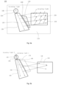
- the diffractive optical waveguide 10 includes a waveguide layer 11 and a diffractive microstructure layer 12 located on a surface of the waveguide layer 11. On a surface of the waveguide layer 11, a region close to a projection optical machine is a coupling-in region 111, and a region close to human eyes is a coupling-out region 112.
- Diffractive microstructures of the coupling-in region 111, the deflecting region 113 and the coupling-out region 112 may be located on the same surface of the waveguide layer 11, or be located on two different surfaces of the waveguide layer 11. As shown in FIG. 1 , the diffractive microstructures of the coupling-in region 111, the deflecting region 113 and the coupling-out region 112 of the diffractive optical waveguide 10 are all located on the same surface of the waveguide layer 11.
- the diffractive microstructure of the coupling-in region 111 utilizes diffraction of light to couple part of signal lights emitted from an optical machine into the waveguide layer 11.
- the diffractive microstructures of the deflecting region 113 and the coupling-out region 112 utilize the diffraction of light to split and expand a beam of light propagated within the deflecting region 113 and the coupling-out region 112 in two dimensions, so that a beam of light incident from the coupling-in region 111 will be expanded into more than one light beam after being propagated and coupled out through the diffractive optical waveguide, namely exit pupil expansion. Referring to FIG.
- the diffractive microstructure layer of the coupling-out region 112 utilizes the diffraction of light to couple lights propagated in the waveguide layer 11 out of the waveguide layer 11.
- the lights coupled out of the waveguide layer 11 are incident to the human eyes, forming an image 20 to be displayed on a retina.
- diffraction efficiency of the diffractive microstructures of the deflecting region 113 and the coupling-out region 112 is constant, which results in attenuation of energy of lights during beam splitting propagation process.
- R0 represents an incident signal light, assuming that energy of the incident signal light is 1, and first-order diffractive efficiency of the diffractive microstructure of the deflecting region 113 to the light is ⁇ ( ⁇ 1), energy of a deflecting light R1, a deflecting light R2 and a deflecting light R3 are respectively ⁇ , (1- ⁇ ) ⁇ and (1- ⁇ ) 2 ⁇ , indicating that energy of deflecting light R1, deflecting light R2 and deflecting light R3 are decreasing.
- order-specific diffraction efficiency of an outgoing light corresponding to the diffractive microstructure of the coupling-out region 112 is ⁇ ( ⁇ 1)
- energy of a coupling-out light R11, R12 and R13 are respectively ⁇ , ⁇ (1- ⁇ ) and ⁇ (1- ⁇ )2 ⁇
- energy of coupling-out light R11, coupling-out light R12 and coupling-out light R13 are decreasing.
- relative energy levels of all coupling-out lights are represented by lengths of the lights, showing a trend of attenuation from an upper left corner of the coupling-out region 112 to a lower right corner of the coupling-out region 112, which will lead to a problem of non-uniform brightness when the waveguide displays an image 30 (referring to FIG. 4 ).
- the purpose of the present disclosure is to provide a diffraction optical waveguide structure, an optical apparatus, and a near-eye display device to solve the technical problem that brightness is not uniform when a waveguide displays images.
- a diffraction optical waveguide structure includes a light-guiding layer, and a coupling-in region, a deflecting region, and a coupling-out region all disposed on the light-guiding layer and sequentially arranged along a direction of an optical path.
- the coupling-in region, the deflecting region and the coupling-out region are all configured with a first diffractive microstructure layer.
- the diffraction optical waveguide structure further includes light-homogenizing region, the light-homogenizing region is arranged between the deflecting region and the coupling-out region.
- the light-homogenizing region is configured with a second diffractive microstructure layer, the second diffractive microstructure layer is configured to spatially redistribute energy of lights to enhance uniformity and brightness of the lights emitted from the coupling-out region.
- the light-homogenizing region is a region enclosed by straight edges; or, the light-homogenizing region is a region enclosed by curved edges.
- the light-homogenizing region includes more than one sub-light-homogenizing region, more than one sub-light-homogenizing region is disposed at intervals, and a distance between two adjacent sub-light-homogenizing regions is less than or equal to 30mm.
- the light-homogenizing region is configured with one or more hole regions, a hole size of the hole region is less than or equal to 30mm.
- the light-homogenizing region is arranged on the same side as the coupling-in region, the deflecting region , and the coupling-out region.
- the light-homogenizing region is disposed between the deflecting region and the coupling-out region, the light-homogenizing region is adjacent to the deflecting region and the coupling-out region;
- At least one of the light-homogenizing region, the coupling-in region, the deflecting region, and the coupling-out region is arranged on a different side from remaining others.
- the light-homogenizing region is disposed between the deflecting region and the coupling-out region, the light-homogenizing region is adjacent to the deflecting region and the coupling-out region in an axial direction;
- an optical apparatus includes a micro-image source and the above-mentioned diffraction optical waveguide structure.
- a near-eye display device includes the above-mentioned optical apparatus.
- a light-homogenizing region is arranged between a deflecting region and a coupling-out region, lights output from the deflecting region may pass completely or partially through the light-homogenizing region before entering the coupling-out region, and the second diffractive microstructure layer disposed in the light-homogenizing region is configured to spatially redistribute energy of lights, which improves the energy of the outgoing lights propagated from the coupling-out region, so as to improve uniformity and overall brightness of the waveguide display, resulting in a better display effect for the diffraction optical waveguide structure.
- 100 diffraction optical waveguide structure; 110, light-guiding layer; 120, coupling-in region; 130, deflecting region; 140, coupling-out region; 150, first diffractive microstructure layer; 160, light-homogenizing region; 161, sub-light-homogenizing region; 162, hole region; 170, second diffractive microstructure layer.
- the diffraction optical waveguide structure 100 includes a light-guiding layer 110, a coupling-in region 120, a deflecting region 130 and a coupling-out region 140.
- the coupling-in region 120, the deflecting region 130 and the coupling-out region 140 are all disposed on the light-guiding layer 110, and are sequentially arranged along a direction of an optical path.
- the coupling-in region 120, the deflecting region 130 and the coupling-out region 140 are all configured with a first diffractive microstructure layer 150.
- the diffraction optical waveguide structure 100 further includes a light-homogenizing region 160, the light-homogenizing region 160 is arranged between the deflecting region 130 and the coupling-out region 140, the light-homogenizing region 160 is configured with a second diffractive microstructure layer 170.
- the second diffractive microstructure layer 170 is configured to spatially redistribute energy of lights, in order to enhance the uniformity and brightness of the lights emitted from the coupling-out region 140.
- the diffraction optical waveguide structure 100 in the present embodiment is configured with a light-homogenizing region 160 arranged between the deflecting region 130 and the coupling-out region 140.
- Lights output from the deflecting region 130 may completely or partially pass through the light-homogenizing region 160 before entering the coupling-out region 140, and the second diffractive microstructure layer 170 disposed in the light-homogenizing region 160 is configured to spatially redistribute energy of lights.
- a light distribution principle of the light-homogenizing region 160 is the same as that of the deflecting region 130, which are both to make one part of lights incident to a corresponding region propagate along an original path, and the other part of the lights propagate towards a predefined direction.
- the light-homogenizing region 160 distributes incoming lights to a right direction and a lower direction.
- the presence of both a solid-arrow outgoing light and a dashed-arrow outgoing light at a certain position of the coupling-out region 140 indicates that intensity of the lights at the certain position is enhanced, resulting in increasing a minimum brightness value of the lights in each field of view.
- the energy of the outgoing lights propagated from the coupling-out region 140 is improved, which improves uniformity and overall brightness of waveguide display, and results in a better display effect for the diffraction optical waveguide structure 100.
- improving uniformity of the waveguide display refers to making brightness of lights from different incident angles as uniform as possible when the lights reaches human eyes, rather than making the brightness of lights from a single angle uniform at various positions of the coupling-out region 140, and the brightness of the lights is as high as possible.
- the diffraction optical waveguide structure 100 provided in the present embodiment has at least the following beneficial effects: the diffraction optical waveguide structure 100 in the present embodiment is configured with a light-homogenizing region 160 arranged between the deflecting region 130 and the coupling-out region 140, lights output from the deflecting region 130 may pass completely or partially through the light-homogenizing region 160 before entering the coupling-out region 140, and the second diffractive microstructure layer 170 disposed in the light-homogenizing region 160 is configured to spatially redistribute energy of lights, which improves the energy of the outgoing lights propagated from the coupling-out region 140, so as to improve uniformity and overall brightness of the waveguide display, resulting in a better display effect for the diffraction optical waveguide structure 100.
- the light-homogenizing region 160 is a region enclosed by straight edges.
- the light-homogenizing region 160 is regularly or irregularly quadrilateral. It should be understood that the light-homogenizing region 160 enclosed by straight edges may also be of other shapes, and is not limited to the above situation, and is not limited herein.
- the light-homogenizing region 160 is a region enclosed by curved edges.
- the light-homogenizing region 160 enclosed by the curved edges is at least one of elliptical and cloud-shaped. It should be understood that the light-homogenizing region 160 may also be of other shapes, and is not limited to the above situation, and is not limited herein.
- the light-homogenizing region 160 includes more than one sub-light-homogenizing region 161, more than one sub-light-homogenizing region 161 is disposed at intervals, and a distance between two adjacent sub-light-homogenizing regions 161 is less than or equal to 30mm.
- the second diffractive microstructure layer 170 in each sub-light-homogenizing region 161 may have different duty cycles and groove depths, and light diffraction efficiency may be modulated by the different duty cycles and groove depths, resulting in assisting spatial distribution of light energy.
- the light-homogenizing region 160 includes 2 to 10 sub-light-homogenizing regions 161. In one embodiment, the light-homogenizing region 160 includes 6 sub-light-homogenizing regions 161.
- a distance between two adjacent sub-light-homogenizing regions 161 ranges from 5mm to 25mm. In one embodiment, the distance between two adjacent the sub-light-homogenizing regions 161 is 5mm. In one embodiment, the distance between two adjacent sub-light-homogenizing regions 161 is 10mm. In one embodiment, the distance between two adjacent sub-light-homogenizing regions 161 is 25mm.
- the number of the sub-light-homogenizing regions 161 in the light-homogenizing region 160, as well as the distance between two adjacent sub-light-homogenizing regions 161 is not limited to the above situation, and may also be other situations, which are not limited herein.
- the light-homogenizing region 160 is configured with one or more hole regions 162, and a hole size of the hole region 162 is less than or equal to 30mm.
- a second diffractive microstructure layer 170 is configured in a region other than the hole region 162 of the light-homogenizing region 160, that is, the second diffractive microstructure layer 170 is not configured in the hole region 162.
- Lights undergo total internal reflection in the hole region 162 of the light-homogenizing region 160, without changing propagation direction and energy. The lights are diffracted in a region other than the hole region 162, and a portion of the light energy is propagated to other directions to participate in energy redistribution.
- the light-homogenizing region 160 is configured with more than one hole region 162, shapes and sizes of more than one hole region 162 may be the same or different, and there are no limitations herein.
- the hole size of the hole region 162 ranges from 5mm to 25mm. In one embodiment, the hole size of the hole region 162 is 5mm. In one embodiment, the hole size of the hole region 162 is 10mm. In one embodiment, the hole size of the hole region 162 is 25mm. It should be understood that the hole size of the hole region 162 is not limited to the above situation, but may be other situations, and there is no limitations herein.
- the light-homogenizing region 160 is arranged on the same side as the coupling-in region 120, the deflecting region 130, and the coupling-out region 140.
- the light-homogenizing region 160 is disposed between the deflecting region 130 and the coupling-out region 140.
- the light-homogenizing region 160 is adjacent to the deflecting region 130 and the coupling-out region 140. That is, a distance between the light-homogenizing region 160 and the deflecting region 130 is zero, and a distance between the light-homogenizing region 160 and the coupling-out region 140 is zero.
- the light-homogenizing region 160 is disposed between the deflecting region 130 and the coupling-out region 140.
- the light-homogenizing region 160 is spaced apart from the deflecting region 130 and the coupling-out region 140.
- a distance between the light-homogenizing region 160 and the deflecting region 130 is less than or equal to 40mm, and a distance between the light-homogenizing region 160 and the coupling-out region 140 is less than or equal to 40mm.
- a distance between the light-homogenizing region 160 and the deflecting region 130 ranges from 10mm to 30mm
- a distance between the light-homogenizing region 160 and the coupling-out region 140 ranges from 10mm to 30mm.
- the distance between the light-homogenizing region 160 and the deflecting region 130 is 10mm, and the distance between the light-homogenizing region 160 and the coupling-out region 140 is 10mm.
- the distance between the light-homogenizing region 160 and the deflecting region 130 is 20mm, and the distance between the light-homogenizing region 160 and the coupling-out region 140 is 20mm.
- the distance between the light-homogenizing region 160 and the deflecting region 130 is 30mm, and the distance between the light-homogenizing region 160 and the coupling-out region 140 is 30mm.
- the distance between the light-homogenizing region 160 and the deflecting region 130, as well as the distance between the light-homogenizing region 160 and the coupling-out region 140 are not limited to the above values, but may also be other values, which are not limited herein.
- the light-homogenizing region 160 is disposed between the deflecting region 130 and the coupling-out region 140.
- the light-homogenizing region 160 is adjacent to the deflecting region 130, that is, a distance between the light-homogenizing region 160 and the deflecting region 130 is zero.
- the light-homogenizing region 160 is spaced apart from the coupling-out region 140, and a distance between the light-homogenizing region 160 and the coupling-out region 140 is less than or equal to 40mm.
- the distance between the light-homogenizing region 160 and the coupling-out region 140 ranges from 10mm to 30mm. In one embodiment, the distance between the light-homogenizing region 160 and the coupling-out region 140 is 10mm. In one embodiment, the distance between the light-homogenizing region 160 and the coupling-out region 140 is 20mm. In one embodiment, the distance between the light-homogenizing region 160 and the coupling-out region 140 is 30mm. It should be understood that the distance between the light-homogenizing region 160 and the coupling-out region 140 is not limited to the above values, but may also be other values, which are not limited herein.
- the light-homogenizing region 160 is disposed between the deflecting region 130 and the coupling-out region 140.
- the light-homogenizing region 160 is adjacent to the coupling-out region 140, that is, a distance between the light-homogenizing region 160 and the coupling-out region 140 is zero.
- the light-homogenizing region 160 is spaced apart from the deflecting region 130, and a distance between the light-homogenizing region 160 and the deflecting region 130 is less than or equal to 40mm.
- the distance between the light-homogenizing region 160 and the deflecting region 130 ranges from 10mm to 30mm. In one embodiment, the distance between the light-homogenizing region 160 and the deflecting region 130 is 10mm. In one embodiment, the distance between the light-homogenizing region 160 and the deflecting region 130 is 20mm. In one embodiment, the distance between the light-homogenizing region 160 and the deflecting region 130 is 30mm. It should be understood that the distance between the light-homogenizing region 160 and the deflecting region 130 is not limited to the above values, but may also be other values, which are not limited herein.
- At least one of the light-homogenizing region 160, the coupling-in region 120, the deflecting region 130, and the coupling-out region 140 is arranged on a different side from remaining others.
- the light-homogenizing region 160 is disposed between the deflecting region 130 and the coupling-out region 140.
- the light-homogenizing region 160 is adjacent to the deflecting region 130 and the coupling-out region 140 in an axial direction. That is, a distance between the light-homogenizing region 160 and the deflecting region 130 is zero, and a distance between the light-homogenizing region 160 and the coupling-out region 140 is zero.
- the light-homogenizing region 160 is disposed between the deflecting region 130 and the coupling-out region 140.
- the light-homogenizing region 160 is spaced apart from the deflecting region 130 and the coupling-out region 140 in an axial direction.
- a distance between the light-homogenizing region 160 and the deflecting region 130 is less than or equal to 40mm, and a distance between the light-homogenizing region 160 and the coupling-out region 140 is less than or equal to 40mm.
- the distance between the light-homogenizing region 160 and the deflecting region 130 ranges from 10mm to 30mm, and the distance between the light-homogenizing region 160 and the coupling-out region 140 ranges from 10mm to 30mm.
- the distance between the light-homogenizing region 160 and the deflecting region 130 is 10mm, and the distance between the light-homogenizing region 160 and the coupling-out region 140 is 10mm.
- the distance between the light-homogenizing region 160 and the deflecting region 130 is 20mm, and the distance between the light-homogenizing region 160 and the coupling-out region 140 is 20mm.
- the distance between the light-homogenizing region 160 and the deflecting region 130 is 30mm, and the distance between the light-homogenizing region 160 and the coupling-out region 140 is 30mm.
- the distance between the light-homogenizing region 160 and the deflecting region 130, as well as the distance between the light-homogenizing region 160 and the coupling-out region 140 are not limited to the above values, but may also be other values, which are not limited herein.
- the light-homogenizing region 160 is disposed between the deflecting region 130 and the coupling-out region 140.
- the light-homogenizing region 160 is adjacent to the deflecting region 130 in an axial direction, that is, a distance between the light-homogenizing region 160 and the deflecting region 130 in the axial direction is zero.
- the light-homogenizing region 160 is spaced apart from the coupling-out region 140 in the axial direction, and a distance between the light-homogenizing region 160 and the coupling-out region 140 is less than or equal to 40mm.
- the distance between the light-homogenizing region 160 and the coupling-out region 140 ranges from 10mm to 30mm. In one embodiment, the distance between the light-homogenizing region 160 and the coupling-out region 140 is 10mm. In one embodiment, the distance between the light-homogenizing region 160 and the coupling-out region 140 is 20mm. In one embodiment, the distance between the light-homogenizing region 160 and the coupling-out region 140 is 30mm. It should be understood that the distance between the light-homogenizing region 160 and the coupling-out region 140 is not limited to the above values, but may also be other values, which are not limited herein.
- the light-homogenizing region 160 is disposed between the deflecting region 130 and the coupling-out region 140.
- the light-homogenizing region 160 is adjacent to the coupling-out region 140 in the axial direction, that is, a distance between the light-homogenizing region 160 and the coupling-out region 140 in the axial direction is zero.
- the light-homogenizing region 160 is spaced apart from the deflecting region 130 in the axial direction, and a distance between the light-homogenizing region 160 and the deflecting region 130 is less than or equal to 40mm.
- the distance between the light-homogenizing region 160 and the deflecting region 130 ranges from 10mm to 30mm. In one embodiment, the distance between the light-homogenizing region 160 and the deflecting region 130 is 10mm. In one embodiment, the distance between the light-homogenizing region 160 and the deflecting region 130 is 20mm. In one embodiment, the distance between the light-homogenizing region 160 and the deflecting region 130 is 30mm. It should be understood that the distance between the light-homogenizing region 160 and the deflecting region 130 is not limited to the above values, but may also be other values, which are not limited herein.
- the light-homogenizing region 160 is disposed between the deflecting region 130 and the coupling-out region 140, and the light-homogenizing region 160 overlaps with at least one of the deflecting region 130 and the coupling-out region 140 in the axial direction.
- the light-homogenizing region 160 overlaps with the deflecting region 130.
- the light-homogenizing region 160 overlaps with the coupling-out region 140.
- the light-homogenizing region 160 overlaps with the deflecting region 130 and the coupling-out region 140.
- a length of an overlap between the light-homogenizing region 160 and the deflecting region 130 ranges from 0mm to 100mm.
- a length of an overlap between the light-homogenizing region 160 and the coupling-out region 140 ranges from 0mm to 100mm.
- the length of an overlap between the light-homogenizing region 160 and the deflecting region 130 is 50mm.
- the length of an overlap between the light-homogenizing region 160 and the coupling-out region 140 is 50mm.
- a length of an overlap between the light-homogenizing region 160 and the deflecting region 130, a length of an overlap between the light-homogenizing region 160 and the coupling-out region 140, are both 50mm. It should be understood that the above-described overlap length is not limited to the above-described values, but may also be other values, which are not limited herein.
- the present embodiment also provides an optical apparatus (not shown in the drawings, the same below), including a micro-image source and the above-mentioned diffraction optical waveguide structure 100. Since the diffraction optical waveguide structure 100 has been described in detail above, it will not be described in detail herein.
- the present embodiment also provides a near-eye display device (not shown in the drawings, the same below), including the above-mentioned optical apparatus.
- the present embodiment provides a diffraction optical waveguide structure 100.
- the diffraction optical waveguide structure 100 includes a light-guiding layer 110, a coupling-in region 120, a deflecting region 130 and a coupling-out region 140.
- the coupling-in region 120, the deflecting region 130 and the coupling-out region 140 are all disposed on the light-guiding layer 110, and are sequentially arranged along a direction of an optical path.
- the coupling-in region 120, the deflecting region 130 and the coupling-out region 140 are all configured with a first diffractive microstructure layer 150.
- the diffraction optical waveguide structure 100 further includes a light-homogenizing region 160, the light-homogenizing region 160 is arranged between the deflecting region 130 and the coupling-out region 140, the light-homogenizing region 160 is configured with a second diffractive microstructure layer 170, the second diffractive microstructure layer 170 is configured to spatially redistribute energy of lights, in order to enhance the uniformity and brightness of the lights emitted from the coupling-out region 140.
- the present embodiment also provides an optical apparatus, including a micro-image source and the above-mentioned diffraction optical waveguide structure 100.
- the present embodiment further provides a near-eye display device, including the above-mentioned optical apparatus.
- the diffraction optical waveguide structure 100, the optical apparatus and the near-eye display device provided in the present embodiment are configured with a light-homogenizing region 160 arranged between the deflecting region 130 and the coupling-out region 140.
- Lights output from the deflecting region 130 may completely or partially pass through the light-homogenizing region 160 before entering the coupling-out region 140, and the second diffractive microstructure layer 170 disposed in the light-homogenizing region 160 is configured to spatially redistribute energy of lights to improve energy of outgoing lights propagated from the coupling-out region 140, thus improving uniformity of waveguide display and improving overall brightness, resulting in a better display effect.
Landscapes
- Physics & Mathematics (AREA)
- General Physics & Mathematics (AREA)
- Optics & Photonics (AREA)
- Engineering & Computer Science (AREA)
- Microelectronics & Electronic Packaging (AREA)
- Optical Couplings Of Light Guides (AREA)
Abstract
Description
- This Application is a National Stage of International Application No.
PCT /CN2023/100751, filed on Jun. 16, 2023 Chinese Application No. 202210740859.0, filed on Jun. 28, 2022 - The present disclosure relates to the technical field of optical technology, and in particularly to a diffraction optical waveguide structure, an optical apparatus and a near-eye display device.
- An optical waveguide is a device capable of confining a signal light within its structure and propagating the signal light along a specific direction, while the optical waveguide exhibits good light transmission. Based on these characteristics, the optical waveguide can be used as a display of an augmented reality (AR) near-eye display device. The optical waveguide directionally propagates signal light emitted from a projection optical machine to human eyes, so the human eyes may observe an displayed image. Furthermore, due to the optical waveguide exhibits good light transmission, the human eyes may also clearly perceive real environment behind the optical waveguide. Therefore, what the human eyes ultimately observes is a fusion of the displayed image and the real environment.
- The optical waveguide may be categorized into different types, such as a geometric optical waveguide, a diffractive optical waveguide, according to different implementation principles. Since a diffractive optical waveguide is thin, lightweight and has good light transmission, the diffractive optical waveguide gradually becomes a preferred solution of the display of the augmented reality (AR) near-eye display device. Referring to
FIG. 1 , the diffractiveoptical waveguide 10 includes awaveguide layer 11 and adiffractive microstructure layer 12 located on a surface of thewaveguide layer 11. On a surface of thewaveguide layer 11, a region close to a projection optical machine is a coupling-inregion 111, and a region close to human eyes is a coupling-outregion 112. There may be adeflecting region 113 positioned between the coupling-inregion 111 and the coupling-outregion 112. Diffractive microstructures of the coupling-inregion 111, thedeflecting region 113 and the coupling-outregion 112 may be located on the same surface of thewaveguide layer 11, or be located on two different surfaces of thewaveguide layer 11. As shown inFIG. 1 , the diffractive microstructures of the coupling-inregion 111, thedeflecting region 113 and the coupling-outregion 112 of the diffractiveoptical waveguide 10 are all located on the same surface of thewaveguide layer 11. - The diffractive microstructure of the coupling-in
region 111 utilizes diffraction of light to couple part of signal lights emitted from an optical machine into thewaveguide layer 11. The diffractive microstructures of thedeflecting region 113 and the coupling-outregion 112 utilize the diffraction of light to split and expand a beam of light propagated within thedeflecting region 113 and the coupling-outregion 112 in two dimensions, so that a beam of light incident from the coupling-inregion 111 will be expanded into more than one light beam after being propagated and coupled out through the diffractive optical waveguide, namely exit pupil expansion. Referring toFIG. 2 , in light propagation process, for an optical waveguide with thedeflecting region 113, more than one light beam is propagated in thewaveguide layer 11 and pass through thedeflecting region 113, then more than one light beam is propagated to the coupling-outregion 112 through total internal reflection. The diffractive microstructure layer of the coupling-outregion 112 utilizes the diffraction of light to couple lights propagated in thewaveguide layer 11 out of thewaveguide layer 11. The lights coupled out of thewaveguide layer 11 are incident to the human eyes, forming animage 20 to be displayed on a retina. - For lights with a particular propagation angle and a diffractive microstructure with a constant period, diffraction efficiency of the diffractive microstructures of the
deflecting region 113 and the coupling-outregion 112 is constant, which results in attenuation of energy of lights during beam splitting propagation process. Referring toFIG. 3 , R0 represents an incident signal light, assuming that energy of the incident signal light is 1, and first-order diffractive efficiency of the diffractive microstructure of thedeflecting region 113 to the light is α(α<1), energy of a deflecting light R1, a deflecting light R2 and a deflecting light R3 are respectively α, (1-α) α and (1-α) 2α, indicating that energy of deflecting light R1, deflecting light R2 and deflecting light R3 are decreasing. Similarly order-specific diffraction efficiency of an outgoing light corresponding to the diffractive microstructure of the coupling-outregion 112 is β(β<1), then energy of a coupling-out light R11, R12 and R13 are respectively αβ, α(1-β) and α(1-β)2β, energy of coupling-out light R11, coupling-out light R12 and coupling-out light R13 are decreasing. InFIG. 3 , relative energy levels of all coupling-out lights are represented by lengths of the lights, showing a trend of attenuation from an upper left corner of the coupling-outregion 112 to a lower right corner of the coupling-outregion 112, which will lead to a problem of non-uniform brightness when the waveguide displays an image 30 (referring toFIG. 4 ). - The purpose of the present disclosure is to provide a diffraction optical waveguide structure, an optical apparatus, and a near-eye display device to solve the technical problem that brightness is not uniform when a waveguide displays images.
- In order to achieve the above purpose, the technical solution of the present disclosure is as follows.
- According to a first aspect of the present invention, a diffraction optical waveguide structure is provided. The diffraction optical waveguide structure includes a light-guiding layer, and a coupling-in region, a deflecting region, and a coupling-out region all disposed on the light-guiding layer and sequentially arranged along a direction of an optical path. The coupling-in region, the deflecting region and the coupling-out region are all configured with a first diffractive microstructure layer. The diffraction optical waveguide structure further includes light-homogenizing region, the light-homogenizing region is arranged between the deflecting region and the coupling-out region. The light-homogenizing region is configured with a second diffractive microstructure layer, the second diffractive microstructure layer is configured to spatially redistribute energy of lights to enhance uniformity and brightness of the lights emitted from the coupling-out region.
- Optionally, the light-homogenizing region is a region enclosed by straight edges; or, the light-homogenizing region is a region enclosed by curved edges.
- Optionally, the light-homogenizing region includes more than one sub-light-homogenizing region, more than one sub-light-homogenizing region is disposed at intervals, and a distance between two adjacent sub-light-homogenizing regions is less than or equal to 30mm.
- Optionally, the light-homogenizing region is configured with one or more hole regions, a hole size of the hole region is less than or equal to 30mm.
- Optionally, the light-homogenizing region is arranged on the same side as the coupling-in region, the deflecting region , and the coupling-out region.
- Optionally, the light-homogenizing region is disposed between the deflecting region and the coupling-out region, the light-homogenizing region is adjacent to the deflecting region and the coupling-out region;
- or, the light-homogenizing region is disposed between the deflecting region and the coupling-out region, the light-homogenizing region is spaced apart from the deflecting region and the coupling-out region, a distance between the light-homogenizing region and the deflecting region is less than or equal to 40mm, and a distance between the light-homogenizing region and the coupling-out region is less than or equal to 40mm;
- or, the light-homogenizing region is disposed between the deflecting region and the coupling-out region, the light-homogenizing region is adjacent to the deflecting region, the light-homogenizing region is spaced apart from the coupling-out region, and a distance between the light-homogenizing region and the coupling-out region is less than or equal to 40mm;
- or, the light-homogenizing region is disposed between the deflecting region and the coupling-out region, the light-homogenizing region is adjacent to the coupling-out region, the light-homogenizing region is spaced apart from the deflecting region, a distance between the light-homogenizing region and the deflecting region is less than or equal to 40mm.
- Optionally,, at least one of the light-homogenizing region, the coupling-in region, the deflecting region, and the coupling-out region is arranged on a different side from remaining others.
- Optionally, the light-homogenizing region is disposed between the deflecting region and the coupling-out region, the light-homogenizing region is adjacent to the deflecting region and the coupling-out region in an axial direction;
- or, the light-homogenizing region is disposed between the deflecting region and the coupling-out region, the light-homogenizing region is spaced apart from the deflecting region and the coupling-out region in an axial direction, a distance between the light-homogenizing region and the deflecting region is less than or equal to 40mm, and a distance between the light-homogenizing region and the coupling-out region is less than or equal to 40mm;
- or, the light-homogenizing region is disposed between the deflecting region and the coupling-out region, the light-homogenizing region is adjacent to the deflecting region in an axial direction, the light-homogenizing region is spaced apart from the coupling-out region in an axial direction, and a distance between the light-homogenizing region and the coupling-out region is less than or equal to 40mm;
- or, the light-homogenizing region is disposed between the deflecting region and the coupling-out region, the light-homogenizing region is adjacent to the coupling-out region in an axial direction, the light-homogenizing region is spaced apart from the deflecting region in an axial direction, and a distance between the light-homogenizing region and the deflecting region is less than or equal to 40mm;
- or, the light-homogenizing region is disposed between the deflecting region and the coupling-out region, and the light-homogenizing region overlaps with at least one of the deflecting region and the coupling-out region in an axial direction.
- According to a first aspect of the present invention, an optical apparatus is provided. The optical apparatus includes a micro-image source and the above-mentioned diffraction optical waveguide structure.
- According to a first aspect of the present invention, a near-eye display device is provided. The near-eye display device includes the above-mentioned optical apparatus.
- In the diffraction optical waveguide structure, an optical apparatus and a near-eye display device of the present disclosure, a light-homogenizing region is arranged between a deflecting region and a coupling-out region, lights output from the deflecting region may pass completely or partially through the light-homogenizing region before entering the coupling-out region, and the second diffractive microstructure layer disposed in the light-homogenizing region is configured to spatially redistribute energy of lights, which improves the energy of the outgoing lights propagated from the coupling-out region, so as to improve uniformity and overall brightness of the waveguide display, resulting in a better display effect for the diffraction optical waveguide structure.
- In order to more clearly illustrate the technical solution of the embodiment of the present disclosure, a brief description will be provided below for the drawings. The drawings described below are provided for some embodiments of the present disclosure, and according to such drawings, those having ordinary skilled in the art may obtain other drawings without any creative endeavor.
-
FIG. 1 is a structural view illustrating a diffraction optical waveguide; -
FIG. 2 is a schematic view illustrating optical path propagation process of a diffraction optical waveguide; -
FIG. 3 is a schematic view illustrating energy attenuation of a diffractive optical waveguide in beam splitting propagation process; -
FIG. 4 is a schematic view illustrating a diffraction optical waveguide, an image displayed by the waveguide exhibits non-uniform brightness; -
FIG. 5a is a first schematic view illustrating a diffraction optical waveguide structure according to one embodiment of the present disclosure; -
FIG. 5b is a second schematic view illustrating a diffraction optical waveguide structure according to one embodiment of the present disclosure; -
FIG. 5c is a third schematic view illustrating a diffraction optical waveguide structure according to one embodiment of the present disclosure; -
FIG. 6 is a fourth schematic view illustrating a diffraction optical waveguide structure according to one embodiment of the present disclosure; -
FIG. 7 is a fifth schematic view illustrating a diffraction optical waveguide structure according to one embodiment of the present disclosure; -
FIG. 8 is a sixth schematic view illustrating a diffraction optical waveguide structure according to one embodiment of the present disclosure; -
FIG. 9 is a seventh schematic view illustrating a diffraction optical waveguide structure according to one embodiment of the present disclosure; -
FIG. 10 is an eighth schematic view illustrating a diffraction optical waveguide structure according to one embodiment of the present disclosure; -
FIG. 11 is a ninth schematic view illustrating a diffraction optical waveguide structure according to one embodiment of the present disclosure; -
FIG. 12 is a tenth schematic view illustrating a diffraction optical waveguide structure according to one embodiment of the present disclosure; -
FIG. 13 is an eleventh schematic view illustrating a diffraction optical waveguide structure according to one embodiment of the present disclosure. - 100, diffraction optical waveguide structure; 110, light-guiding layer; 120, coupling-in region; 130, deflecting region; 140, coupling-out region; 150, first diffractive microstructure layer; 160, light-homogenizing region; 161, sub-light-homogenizing region; 162, hole region; 170, second diffractive microstructure layer.
- To make the objectives, technical solutions, and advantages of the present disclosure clearer and more definite, a detailed description of embodiments of the present disclosure will be further provided below with reference to the attached drawings and embodiments. It is appreciated that the embodiments described herein are provided solely for illustrating the present disclosure and are not to limit the present disclosure.
- It is noted that when a component is referred to as being "fixed" or "arranged" on another component, it can be directly set on another component, or it can be indirectly set on another component. When a component is referred to as being "connected" to another component, it can be directly connected to another component or it can be indirectly connected to another component. Terms that indicate directional or positional relationships, such as "up", "down", "left", "right", "front", "back", "vertical", "horizontal", "top", "bottom", "inner", "outer" are based on the directional or positional relationship illustrated in the attached drawings, and are adopted for easily describing the present disclosure, and are not construed as limiting to present technical solutions. Terms "first" and "second" are adopted for easily describing the present disclosure, and are not construed as indicating or implying relative importance or implying the number of technical features. The meaning of "multiple" is two or more, unless otherwise specifically defined.
- Referring to
FIG. 5 , one embodiment of the present disclosure provides a diffractionoptical waveguide structure 100. The diffractionoptical waveguide structure 100 includes a light-guidinglayer 110, a coupling-inregion 120, a deflectingregion 130 and a coupling-outregion 140. The coupling-inregion 120, the deflectingregion 130 and the coupling-outregion 140 are all disposed on the light-guidinglayer 110, and are sequentially arranged along a direction of an optical path. The coupling-inregion 120, the deflectingregion 130 and the coupling-outregion 140 are all configured with a firstdiffractive microstructure layer 150. The diffractionoptical waveguide structure 100 further includes a light-homogenizing region 160, the light-homogenizing region 160 is arranged between the deflectingregion 130 and the coupling-outregion 140, the light-homogenizing region 160 is configured with a seconddiffractive microstructure layer 170. The seconddiffractive microstructure layer 170 is configured to spatially redistribute energy of lights, in order to enhance the uniformity and brightness of the lights emitted from the coupling-outregion 140. - The working principle of the diffraction
optical waveguide structure 100 provided in the present embodiment is as follows:
the diffractionoptical waveguide structure 100 in the present embodiment is configured with a light-homogenizing region 160 arranged between the deflectingregion 130 and the coupling-outregion 140. Lights output from the deflectingregion 130 may completely or partially pass through the light-homogenizing region 160 before entering the coupling-outregion 140, and the seconddiffractive microstructure layer 170 disposed in the light-homogenizing region 160 is configured to spatially redistribute energy of lights. The specific distribution principle is as follows: a light distribution principle of the light-homogenizing region 160 is the same as that of the deflectingregion 130, which are both to make one part of lights incident to a corresponding region propagate along an original path, and the other part of the lights propagate towards a predefined direction. As shown inFIG. 5 , the light-homogenizing region 160 distributes incoming lights to a right direction and a lower direction. The presence of both a solid-arrow outgoing light and a dashed-arrow outgoing light at a certain position of the coupling-outregion 140 indicates that intensity of the lights at the certain position is enhanced, resulting in increasing a minimum brightness value of the lights in each field of view. It can be seen that the energy of the outgoing lights propagated from the coupling-outregion 140 is improved, which improves uniformity and overall brightness of waveguide display, and results in a better display effect for the diffractionoptical waveguide structure 100. It should be understood that improving uniformity of the waveguide display refers to making brightness of lights from different incident angles as uniform as possible when the lights reaches human eyes, rather than making the brightness of lights from a single angle uniform at various positions of the coupling-outregion 140, and the brightness of the lights is as high as possible. - The diffraction
optical waveguide structure 100 provided in the present embodiment has at least the following beneficial effects:
the diffractionoptical waveguide structure 100 in the present embodiment is configured with a light-homogenizing region 160 arranged between the deflectingregion 130 and the coupling-outregion 140, lights output from the deflectingregion 130 may pass completely or partially through the light-homogenizing region 160 before entering the coupling-outregion 140, and the seconddiffractive microstructure layer 170 disposed in the light-homogenizing region 160 is configured to spatially redistribute energy of lights, which improves the energy of the outgoing lights propagated from the coupling-outregion 140, so as to improve uniformity and overall brightness of the waveguide display, resulting in a better display effect for the diffractionoptical waveguide structure 100. - In one embodiment, referring to
FIGS. 5-7 , the light-homogenizing region 160 is a region enclosed by straight edges. For example: the light-homogenizing region 160 is regularly or irregularly quadrilateral. It should be understood that the light-homogenizing region 160 enclosed by straight edges may also be of other shapes, and is not limited to the above situation, and is not limited herein. - In one embodiment, referring to
FIG. 8 , the light-homogenizing region 160 is a region enclosed by curved edges. For example: the light-homogenizing region 160 enclosed by the curved edges is at least one of elliptical and cloud-shaped. It should be understood that the light-homogenizing region 160 may also be of other shapes, and is not limited to the above situation, and is not limited herein. - In one embodiment, referring to
FIG. 9 , the light-homogenizing region 160 includes more than one sub-light-homogenizing region 161, more than one sub-light-homogenizing region 161 is disposed at intervals, and a distance between two adjacent sub-light-homogenizingregions 161 is less than or equal to 30mm. The seconddiffractive microstructure layer 170 in each sub-light-homogenizing region 161 may have different duty cycles and groove depths, and light diffraction efficiency may be modulated by the different duty cycles and groove depths, resulting in assisting spatial distribution of light energy. - In one embodiment, the light-
homogenizing region 160 includes 2 to 10 sub-light-homogenizingregions 161. In one embodiment, the light-homogenizing region 160 includes 6 sub-light-homogenizingregions 161. - In one embodiment, a distance between two adjacent sub-light-homogenizing
regions 161 ranges from 5mm to 25mm. In one embodiment, the distance between two adjacent the sub-light-homogenizingregions 161 is 5mm. In one embodiment, the distance between two adjacent sub-light-homogenizingregions 161 is 10mm. In one embodiment, the distance between two adjacent sub-light-homogenizingregions 161 is 25mm. - It should be understood that the number of the sub-light-homogenizing
regions 161 in the light-homogenizing region 160, as well as the distance between two adjacent sub-light-homogenizingregions 161 is not limited to the above situation, and may also be other situations, which are not limited herein. - In one embodiment, referring to
FIG. 10 , the light-homogenizing region 160 is configured with one ormore hole regions 162, and a hole size of thehole region 162 is less than or equal to 30mm. It should be understood that a seconddiffractive microstructure layer 170 is configured in a region other than thehole region 162 of the light-homogenizing region 160, that is, the seconddiffractive microstructure layer 170 is not configured in thehole region 162. Lights undergo total internal reflection in thehole region 162 of the light-homogenizing region 160, without changing propagation direction and energy. The lights are diffracted in a region other than thehole region 162, and a portion of the light energy is propagated to other directions to participate in energy redistribution. These two modes in the light-homogenizing region 160 are combined together to provide more freedom for spatial redistribution of energy, and achieve a better display effect for the diffractionoptical waveguide structure 100 when structure of the light-homogenizing region 160 is configured with a large number offine hole regions 162. - In one embodiment, the light-
homogenizing region 160 is configured with more than onehole region 162, shapes and sizes of more than onehole region 162 may be the same or different, and there are no limitations herein. - In one embodiment, the hole size of the
hole region 162 ranges from 5mm to 25mm. In one embodiment, the hole size of thehole region 162 is 5mm. In one embodiment, the hole size of thehole region 162 is 10mm. In one embodiment, the hole size of thehole region 162 is 25mm. It should be understood that the hole size of thehole region 162 is not limited to the above situation, but may be other situations, and there is no limitations herein. - In one embodiment, the light-
homogenizing region 160 is arranged on the same side as the coupling-inregion 120, the deflectingregion 130, and the coupling-outregion 140. - In one embodiment, the light-
homogenizing region 160 is disposed between the deflectingregion 130 and the coupling-outregion 140. The light-homogenizing region 160 is adjacent to the deflectingregion 130 and the coupling-outregion 140. That is, a distance between the light-homogenizing region 160 and the deflectingregion 130 is zero, and a distance between the light-homogenizing region 160 and the coupling-outregion 140 is zero. - In one embodiment, referring to
FIG. 5 , the light-homogenizing region 160 is disposed between the deflectingregion 130 and the coupling-outregion 140. The light-homogenizing region 160 is spaced apart from the deflectingregion 130 and the coupling-outregion 140. A distance between the light-homogenizing region 160 and the deflectingregion 130 is less than or equal to 40mm, and a distance between the light-homogenizing region 160 and the coupling-outregion 140 is less than or equal to 40mm. - When an
incident light 1 and anincident light 2 at different angles propagate between the deflectingregion 130 and the coupling-outregion 140, propagation directions of theincident light 1 and theincident light 2 are different, as shown inFIG. 5b /5c . The same light-homogenizingregions 160 positioned at different positions may have different impact on lights. Different light-homogenizingregions 160 positioned at different positions, may have the same impact on lights. As shown inFIG. 5b /5c , size and position of the light-homogenizingregions 160 are different, but the light-homogenizingregions 160 exert the same effect for both theincident light 1 and the incident light 2.Therefore, the light-homogenizing region 160 inFIG. 5c , which has a smaller processing area, is less costly than the light-homogenizing region 160 inFIG. 5b . - In one embodiment, a distance between the light-
homogenizing region 160 and the deflectingregion 130 ranges from 10mm to 30mm, a distance between the light-homogenizing region 160 and the coupling-outregion 140 ranges from 10mm to 30mm. - In one embodiment, the distance between the light-
homogenizing region 160 and the deflectingregion 130 is 10mm, and the distance between the light-homogenizing region 160 and the coupling-outregion 140 is 10mm. - In one embodiment, the distance between the light-
homogenizing region 160 and the deflectingregion 130 is 20mm, and the distance between the light-homogenizing region 160 and the coupling-outregion 140 is 20mm. - In one embodiment, the distance between the light-
homogenizing region 160 and the deflectingregion 130 is 30mm, and the distance between the light-homogenizing region 160 and the coupling-outregion 140 is 30mm. - It should be understood that the distance between the light-
homogenizing region 160 and the deflectingregion 130, as well as the distance between the light-homogenizing region 160 and the coupling-outregion 140 are not limited to the above values, but may also be other values, which are not limited herein. - In one embodiment, referring to
FIG. 6 , the light-homogenizing region 160 is disposed between the deflectingregion 130 and the coupling-outregion 140. The light-homogenizing region 160 is adjacent to the deflectingregion 130, that is, a distance between the light-homogenizing region 160 and the deflectingregion 130 is zero. The light-homogenizing region 160 is spaced apart from the coupling-outregion 140, and a distance between the light-homogenizing region 160 and the coupling-outregion 140 is less than or equal to 40mm. - In one embodiment, the distance between the light-
homogenizing region 160 and the coupling-outregion 140 ranges from 10mm to 30mm. In one embodiment, the distance between the light-homogenizing region 160 and the coupling-outregion 140 is 10mm. In one embodiment, the distance between the light-homogenizing region 160 and the coupling-outregion 140 is 20mm. In one embodiment, the distance between the light-homogenizing region 160 and the coupling-outregion 140 is 30mm. It should be understood that the distance between the light-homogenizing region 160 and the coupling-outregion 140 is not limited to the above values, but may also be other values, which are not limited herein. - In one embodiment, referring to
FIG. 7 , the light-homogenizing region 160 is disposed between the deflectingregion 130 and the coupling-outregion 140. The light-homogenizing region 160 is adjacent to the coupling-outregion 140, that is, a distance between the light-homogenizing region 160 and the coupling-outregion 140 is zero. The light-homogenizing region 160 is spaced apart from the deflectingregion 130, and a distance between the light-homogenizing region 160 and the deflectingregion 130 is less than or equal to 40mm. - In one embodiment, the distance between the light-
homogenizing region 160 and the deflectingregion 130 ranges from 10mm to 30mm. In one embodiment, the distance between the light-homogenizing region 160 and the deflectingregion 130 is 10mm. In one embodiment, the distance between the light-homogenizing region 160 and the deflectingregion 130 is 20mm. In one embodiment, the distance between the light-homogenizing region 160 and the deflectingregion 130 is 30mm. It should be understood that the distance between the light-homogenizing region 160 and the deflectingregion 130 is not limited to the above values, but may also be other values, which are not limited herein. - In one embodiment, at least one of the light-
homogenizing region 160, the coupling-inregion 120, the deflectingregion 130, and the coupling-outregion 140 is arranged on a different side from remaining others. - In one embodiment, referring to
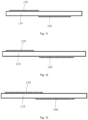
FIG. 11 , the light-homogenizing region 160 is disposed between the deflectingregion 130 and the coupling-outregion 140. The light-homogenizing region 160 is adjacent to the deflectingregion 130 and the coupling-outregion 140 in an axial direction. That is, a distance between the light-homogenizing region 160 and the deflectingregion 130 is zero, and a distance between the light-homogenizing region 160 and the coupling-outregion 140 is zero. - In one embodiment, referring to
FIG. 12 , the light-homogenizing region 160 is disposed between the deflectingregion 130 and the coupling-outregion 140. The light-homogenizing region 160 is spaced apart from the deflectingregion 130 and the coupling-outregion 140 in an axial direction. A distance between the light-homogenizing region 160 and the deflectingregion 130 is less than or equal to 40mm, and a distance between the light-homogenizing region 160 and the coupling-outregion 140 is less than or equal to 40mm. - In one embodiment, the distance between the light-
homogenizing region 160 and the deflectingregion 130 ranges from 10mm to 30mm, and the distance between the light-homogenizing region 160 and the coupling-outregion 140 ranges from 10mm to 30mm. - In one embodiment, the distance between the light-
homogenizing region 160 and the deflectingregion 130 is 10mm, and the distance between the light-homogenizing region 160 and the coupling-outregion 140 is 10mm. - In one embodiment, the distance between the light-
homogenizing region 160 and the deflectingregion 130 is 20mm, and the distance between the light-homogenizing region 160 and the coupling-outregion 140 is 20mm. - In one embodiment, the distance between the light-
homogenizing region 160 and the deflectingregion 130 is 30mm, and the distance between the light-homogenizing region 160 and the coupling-outregion 140 is 30mm. - It should be understood that the distance between the light-
homogenizing region 160 and the deflectingregion 130, as well as the distance between the light-homogenizing region 160 and the coupling-outregion 140 are not limited to the above values, but may also be other values, which are not limited herein. - In one embodiment, the light-
homogenizing region 160 is disposed between the deflectingregion 130 and the coupling-outregion 140. The light-homogenizing region 160 is adjacent to the deflectingregion 130 in an axial direction, that is, a distance between the light-homogenizing region 160 and the deflectingregion 130 in the axial direction is zero. The light-homogenizing region 160 is spaced apart from the coupling-outregion 140 in the axial direction, and a distance between the light-homogenizing region 160 and the coupling-outregion 140 is less than or equal to 40mm. - In one embodiment, the distance between the light-
homogenizing region 160 and the coupling-outregion 140 ranges from 10mm to 30mm. In one embodiment, the distance between the light-homogenizing region 160 and the coupling-outregion 140 is 10mm. In one embodiment, the distance between the light-homogenizing region 160 and the coupling-outregion 140 is 20mm. In one embodiment, the distance between the light-homogenizing region 160 and the coupling-outregion 140 is 30mm. It should be understood that the distance between the light-homogenizing region 160 and the coupling-outregion 140 is not limited to the above values, but may also be other values, which are not limited herein. - In one embodiment, the light-
homogenizing region 160 is disposed between the deflectingregion 130 and the coupling-outregion 140. The light-homogenizing region 160 is adjacent to the coupling-outregion 140 in the axial direction, that is, a distance between the light-homogenizing region 160 and the coupling-outregion 140 in the axial direction is zero. The light-homogenizing region 160 is spaced apart from the deflectingregion 130 in the axial direction, and a distance between the light-homogenizing region 160 and the deflectingregion 130 is less than or equal to 40mm. - In one embodiment, the distance between the light-
homogenizing region 160 and the deflectingregion 130 ranges from 10mm to 30mm. In one embodiment, the distance between the light-homogenizing region 160 and the deflectingregion 130 is 10mm. In one embodiment, the distance between the light-homogenizing region 160 and the deflectingregion 130 is 20mm. In one embodiment, the distance between the light-homogenizing region 160 and the deflectingregion 130 is 30mm. It should be understood that the distance between the light-homogenizing region 160 and the deflectingregion 130 is not limited to the above values, but may also be other values, which are not limited herein. - In one embodiment, referring to
FIG. 13 , the light-homogenizing region 160 is disposed between the deflectingregion 130 and the coupling-outregion 140, and the light-homogenizing region 160 overlaps with at least one of the deflectingregion 130 and the coupling-outregion 140 in the axial direction. - In one embodiment, the light-
homogenizing region 160 overlaps with the deflectingregion 130. - In one embodiment, the light-
homogenizing region 160 overlaps with the coupling-outregion 140. - In one embodiment, the light-
homogenizing region 160 overlaps with the deflectingregion 130 and the coupling-outregion 140. - In one embodiment, a length of an overlap between the light-
homogenizing region 160 and the deflectingregion 130 ranges from 0mm to 100mm. A length of an overlap between the light-homogenizing region 160 and the coupling-outregion 140 ranges from 0mm to 100mm. A length of an overlap between the light-homogenizing region 160 and the deflectingregion 130, a length of an overlap between the light-homogenizing region 160 and the coupling-outregion 140, both range from 0mm to 100mm. - In one embodiment, the length of an overlap between the light-
homogenizing region 160 and the deflectingregion 130 is 50mm. The length of an overlap between the light-homogenizing region 160 and the coupling-outregion 140 is 50mm. A length of an overlap between the light-homogenizing region 160 and the deflectingregion 130, a length of an overlap between the light-homogenizing region 160 and the coupling-outregion 140, are both 50mm. It should be understood that the above-described overlap length is not limited to the above-described values, but may also be other values, which are not limited herein. - The present embodiment also provides an optical apparatus (not shown in the drawings, the same below), including a micro-image source and the above-mentioned diffraction
optical waveguide structure 100. Since the diffractionoptical waveguide structure 100 has been described in detail above, it will not be described in detail herein. - The present embodiment also provides a near-eye display device (not shown in the drawings, the same below), including the above-mentioned optical apparatus.
- In summary, the present embodiment provides a diffraction
optical waveguide structure 100. The diffractionoptical waveguide structure 100 includes a light-guidinglayer 110, a coupling-inregion 120, a deflectingregion 130 and a coupling-outregion 140. The coupling-inregion 120, the deflectingregion 130 and the coupling-outregion 140 are all disposed on the light-guidinglayer 110, and are sequentially arranged along a direction of an optical path. The coupling-inregion 120, the deflectingregion 130 and the coupling-outregion 140 are all configured with a firstdiffractive microstructure layer 150. The diffractionoptical waveguide structure 100 further includes a light-homogenizing region 160, the light-homogenizing region 160 is arranged between the deflectingregion 130 and the coupling-outregion 140, the light-homogenizing region 160 is configured with a seconddiffractive microstructure layer 170, the seconddiffractive microstructure layer 170 is configured to spatially redistribute energy of lights, in order to enhance the uniformity and brightness of the lights emitted from the coupling-outregion 140. The present embodiment also provides an optical apparatus, including a micro-image source and the above-mentioned diffractionoptical waveguide structure 100. The present embodiment further provides a near-eye display device, including the above-mentioned optical apparatus. The diffractionoptical waveguide structure 100, the optical apparatus and the near-eye display device provided in the present embodiment, are configured with a light-homogenizing region 160 arranged between the deflectingregion 130 and the coupling-outregion 140. Lights output from the deflectingregion 130 may completely or partially pass through the light-homogenizing region 160 before entering the coupling-outregion 140, and the seconddiffractive microstructure layer 170 disposed in the light-homogenizing region 160 is configured to spatially redistribute energy of lights to improve energy of outgoing lights propagated from the coupling-outregion 140, thus improving uniformity of waveguide display and improving overall brightness, resulting in a better display effect. - The above are only preferred embodiments of the present disclosure, and are not intended to limit the present disclosure. Any modification, equivalent substitution and improvement made within the spirit and principle of the present disclosure should be included in the protection scope of the present disclosure.
Claims (15)
- A diffraction optical waveguide structure (100), comprising:a light-guiding layer (110), and a coupling-in region (120), a deflecting region (130), and a coupling-out region (140) all disposed on the light-guiding layer (110) and sequentially arranged along a direction of an optical path, the coupling-in region (120), the deflecting region (130) and the coupling-out region (140) are all configured with a first diffractive microstructure layer (150);the diffraction optical waveguide structure (100) further comprises light-homogenizing region (160), the light-homogenizing region (160) is arranged between the deflecting region (130) and the coupling-out region (140), the light-homogenizing region (160) is configured with a second diffractive microstructure layer (170), the second diffractive microstructure layer (170) is configured to spatially redistribute energy of lights to enhance uniformity and brightness of the lights emitted from the coupling-out region (140).
- The diffraction optical waveguide structure (100) according to claim 1, wherein the light-homogenizing region (160) is a region enclosed by straight edges; or, the light-homogenizing region (160) is a region enclosed by curved edges.
- The diffraction optical waveguide structure (100) according to claim 1, wherein the light-homogenizing region (160) includes more than one sub-light-homogenizing region (161), more than one sub-light-homogenizing region (161) is disposed at intervals, and a distance between two adjacent sub-light-homogenizing regions (161) is less than or equal to 30mm.
- The diffraction optical waveguide structure (100) according to claim 1, wherein the light-homogenizing region (160) is configured with one or more hole regions (162), a hole size of the hole region (162) is less than or equal to 30mm.
- The diffraction optical waveguide structure (100) according to any one of claims 1 to 4, wherein the light-homogenizing region (160) is arranged on the same side as the coupling-in region (120), the deflecting region (130) , and the coupling-out region (140).
- The diffraction optical waveguide structure (100) according to claim 5, wherein the light-homogenizing region (160) is disposed between the deflecting region (130) and the coupling-out region (140), the light-homogenizing region (160) is adjacent to the deflecting region (130) and the coupling-out region (140);or, the light-homogenizing region (160) is disposed between the deflecting region (130) and the coupling-out region (140), the light-homogenizing region (160) is spaced apart from the deflecting region (130) and the coupling-out region (140), a distance between the light-homogenizing region (160) and the deflecting region (130) is less than or equal to 40mm, and a distance between the light-homogenizing region (160) and the coupling-out region (140) is less than or equal to 40mm;or, the light-homogenizing region (160) is disposed between the deflecting region (130) and the coupling-out region (140), the light-homogenizing region (160) is adjacent to the deflecting region (130), the light-homogenizing region (160) is spaced apart from the coupling-out region (140), and a distance between the light-homogenizing region (160) and the coupling-out region (140) is less than or equal to 40mm;or, the light-homogenizing region (160) is disposed between the deflecting region (130) and the coupling-out region (140), the light-homogenizing region (160) is adjacent to the coupling-out region (140), the light-homogenizing region (160) is spaced apart from the deflecting region (130), a distance between the light-homogenizing region (160) and the deflecting region (130) is less than or equal to 40mm.
- The diffraction optical waveguide structure (100) according to any one of claims 1 to 4, wherein at least one of the light-homogenizing region (160), the coupling-in region (120), the deflecting region (130), and the coupling-out region (140) is arranged on a different side from remaining others.
- The diffraction optical waveguide structure (100) according to claim 7, wherein the light-homogenizing region (160) is disposed between the deflecting region (130) and the coupling-out region (140), the light-homogenizing region (160) is adjacent to the deflecting region (130) and the coupling-out region (140) in an axial direction;or, the light-homogenizing region (160) is disposed between the deflecting region (130) and the coupling-out region (140), the light-homogenizing region (160) is spaced apart from the deflecting region (130) and the coupling-out region (140) in an axial direction, a distance between the light-homogenizing region (160) and the deflecting region (130) is less than or equal to 40mm, and a distance between the light-homogenizing region (160) and the coupling-out region (140) is less than or equal to 40mm;or, the light-homogenizing region (160) is disposed between the deflecting region (130) and the coupling-out region (140), the light-homogenizing region (160) is adjacent to the deflecting region (130) in an axial direction, the light-homogenizing region (160) is spaced apart from the coupling-out region (140) in an axial direction, and a distance between the light-homogenizing region (160) and the coupling-out region (140) is less than or equal to 40mm;or, the light-homogenizing region (160) is disposed between the deflecting region (130) and the coupling-out region (140), the light-homogenizing region (160) is adjacent to the coupling-out region (140) in an axial direction, the light-homogenizing region (160) is spaced apart from the deflecting region (130) in an axial direction, and a distance between the light-homogenizing region (160) and the deflecting region (130) is less than or equal to 40mm;or, the light-homogenizing region (160) is disposed between the deflecting region (130) and the coupling-out region (140), and the light-homogenizing region (160) overlaps with at least one of the deflecting region (130) and the coupling-out region (140) in an axial direction.
- The diffraction optical waveguide structure (100) according to claim 1, wherein the light-homogenizing region (160) comprises more than one sub-light-homogenizing regions (161), the second diffractive microstructure layer (170) in each the sub-light-homogenizing region (161) has different duty cycles and groove depths.
- The diffraction optical waveguide structure (100) according to claim 1, wherein the light-homogenizing region (160) is configured with one or more hole regions (162), a second diffractive microstructure layer (170) is configured in a region other than the hole region (162) of the light-homogenizing region (160).
- The diffraction optical waveguide structure (100) according to claim 1, wherein the light-homogenizing region (160) is configured with more than one hole region (162).
- The diffraction optical waveguide structure (100) according to claim 1, wherein the light-homogenizing region (160) is disposed between the deflecting region (130) and the coupling-out region (140), a distance between the light-homogenizing region (160) and the deflecting region (130) is greater than a distance between the light-homogenizing region (160) and the coupling-out region (140).
- The diffraction optical waveguide structure (100) according to claim 1, wherein the light-homogenizing region (160) is disposed between the deflecting region (130) and the coupling-out region (140), a distance between the light-homogenizing region (160) and the deflecting region (130) ranges from 10mm to 30mm, a distance between the light-homogenizing region (160) and the coupling-out region (140) ranges from 10mm to 30mm.
- An optical apparatus, comprising: a micro-image source, and a diffraction optical waveguide structure (100) according to any one of claims 1 to 13.
- A near-eye display device, comprising: an optical apparatus according to claim 14.
Applications Claiming Priority (2)
| Application Number | Priority Date | Filing Date | Title |
|---|---|---|---|
| CN202210740859.0A CN115016061A (en) | 2022-06-28 | 2022-06-28 | Diffraction light waveguide structure, optical device and near-to-eye display equipment |
| PCT/CN2023/100751 WO2024001830A1 (en) | 2022-06-28 | 2023-06-16 | Diffractive optical waveguide structure, optical apparatus, and near-eye display device |
Publications (2)
| Publication Number | Publication Date |
|---|---|
| EP4571390A1 true EP4571390A1 (en) | 2025-06-18 |
| EP4571390A4 EP4571390A4 (en) | 2025-10-15 |
Family
ID=83077562
Family Applications (1)
| Application Number | Title | Priority Date | Filing Date |
|---|---|---|---|
| EP23830010.7A Pending EP4571390A4 (en) | 2022-06-28 | 2023-06-16 | DIFFRACTION OPTICAL WAVEGUIDE STRUCTURE, OPTICAL APPARATUS AND NEAR-EYE DISPLAY DEVICE |
Country Status (4)
| Country | Link |
|---|---|
| US (1) | US20250053014A1 (en) |
| EP (1) | EP4571390A4 (en) |
| CN (1) | CN115016061A (en) |
| WO (1) | WO2024001830A1 (en) |
Families Citing this family (1)
| Publication number | Priority date | Publication date | Assignee | Title |
|---|---|---|---|---|
| CN115016061A (en) * | 2022-06-28 | 2022-09-06 | 珠海莫界科技有限公司 | Diffraction light waveguide structure, optical device and near-to-eye display equipment |
Family Cites Families (19)
| Publication number | Priority date | Publication date | Assignee | Title |
|---|---|---|---|---|
| EP3667399A1 (en) * | 2007-06-04 | 2020-06-17 | Magic Leap, Inc. | A diffractive beam expander |
| US10698214B2 (en) * | 2017-01-17 | 2020-06-30 | Microsoft Technology Licensing, Llc | Optical device to improve image uniformity |
| CN113281839B (en) * | 2017-06-13 | 2023-04-14 | 伊奎蒂公司 | Image light guide with overlapping grating for enlarged light distribution |
| US11982827B2 (en) * | 2018-01-12 | 2024-05-14 | Lg Chem, Ltd. | Diffraction light guide plate and display device including the same |
| WO2020150276A1 (en) * | 2019-01-14 | 2020-07-23 | Vuzix Corporation | Digital writing of large diffraction grating patterns |
| US11391950B2 (en) * | 2019-06-26 | 2022-07-19 | Meta Platforms Technologies, Llc | Techniques for controlling effective refractive index of gratings |
| US20210055551A1 (en) * | 2019-08-23 | 2021-02-25 | Facebook Technologies, Llc | Dispersion compensation in volume bragg grating-based waveguide display |
| CN112731659B (en) * | 2019-10-14 | 2024-12-31 | 苏州苏大维格科技集团股份有限公司 | Waveguide display lenses and augmented reality glasses |
| US20240103270A1 (en) * | 2019-11-06 | 2024-03-28 | Google Llc | Optical combiners with improved efficiency and uniformity |
| CN111123524A (en) * | 2020-01-17 | 2020-05-08 | 北京枭龙科技有限公司 | Diffraction waveguide capable of expanding pupil and uniformly emitting light |
| CN212433445U (en) * | 2020-06-24 | 2021-01-29 | 深圳珑璟光电科技有限公司 | Optical waveguide and near-to-eye display system |
| CN111812760B (en) * | 2020-08-06 | 2024-01-30 | 深圳珑璟光电技术有限公司 | Grating structure, optical waveguide and near-to-eye display system |
| CN113777703B (en) * | 2021-08-25 | 2024-06-04 | 宁波舜宇奥来技术有限公司 | Optical waveguide structure and near-to-eye display |
| CN113721320A (en) * | 2021-09-06 | 2021-11-30 | 宁波舜宇奥来技术有限公司 | Optical waveguide structure and display device |
| CN114200570B (en) * | 2021-12-31 | 2023-10-03 | 珠海莫界科技有限公司 | A multi-layer diffractive optical waveguide device and near-eye display device |
| CN114217375B (en) * | 2021-12-31 | 2023-08-29 | 珠海莫界科技有限公司 | High-brightness uniformity diffraction optical waveguide device and head-mounted AR display device |
| CN114355502B (en) * | 2022-02-17 | 2024-01-30 | 烟台艾睿光电科技有限公司 | Diffraction grating waveguide and AR display device |
| CN217879712U (en) * | 2022-06-28 | 2022-11-22 | 珠海莫界科技有限公司 | Diffraction light waveguide structure, optical device and near-to-eye display equipment |
| CN115016061A (en) * | 2022-06-28 | 2022-09-06 | 珠海莫界科技有限公司 | Diffraction light waveguide structure, optical device and near-to-eye display equipment |
-
2022
- 2022-06-28 CN CN202210740859.0A patent/CN115016061A/en active Pending
-
2023
- 2023-06-16 WO PCT/CN2023/100751 patent/WO2024001830A1/en not_active Ceased
- 2023-06-16 EP EP23830010.7A patent/EP4571390A4/en active Pending
-
2024
- 2024-10-24 US US18/925,071 patent/US20250053014A1/en active Pending
Also Published As
| Publication number | Publication date |
|---|---|
| EP4571390A4 (en) | 2025-10-15 |
| CN115016061A (en) | 2022-09-06 |
| WO2024001830A1 (en) | 2024-01-04 |
| US20250053014A1 (en) | 2025-02-13 |
Similar Documents
| Publication | Publication Date | Title |
|---|---|---|
| KR102699716B1 (en) | Optical Systems including Light-Guide Optical Elements with Two-Dimensional Expansion | |
| EP4300165B1 (en) | Diffractive optical waveguide and display device | |
| CN214474235U (en) | near-eye display device | |
| JP2021517265A (en) | Exit pupil magnifier | |
| JP2020521994A (en) | Display element, personal display device, method for producing an image on a personal display, and use | |
| EP4310576B1 (en) | Diffractive optical waveguide and display device | |
| EP3757660A1 (en) | Optical apparatus | |
| CN115113323B (en) | Diffraction light waveguide and display equipment | |
| CN113777707A (en) | Optical structure and optical device | |
| JP7566355B2 (en) | Apparatus for displaying augmented reality images and system including the same - Patents.com | |
| WO2023029319A1 (en) | Augmented reality diffractive optical waveguide and augmented reality display apparatus | |
| CN211928226U (en) | Optical waveguide lens and three-dimensional display device | |
| JP3214997U (en) | Backlight module and display device | |
| EP4418031B1 (en) | Diffractive optical waveguide and display device | |
| CN215641931U (en) | Optical structures and optical devices | |
| EP4571390A1 (en) | Diffractive optical waveguide structure, optical apparatus, and near-eye display device | |
| WO2021169405A1 (en) | Optical waveguide lens capable of multi-directional diffraction expansion, and augmented reality display device | |
| KR20220052262A (en) | Waveguide structure with segmented diffractive optical elements and near-eye display apparatus employing the same | |
| US12474517B1 (en) | Light guide device, optical display system and display device | |
| JP4738798B2 (en) | Image observation device | |
| CN217879712U (en) | Diffraction light waveguide structure, optical device and near-to-eye display equipment | |
| CN115079334B (en) | Diffractive waveguide device and method | |
| CN106255915A (en) | Transmission type screen and head-up display | |
| CN115586636B (en) | An optical pupil expander, device, method, and display device | |
| CN216144979U (en) | Augmented reality diffraction optical waveguide and augmented reality display device |
Legal Events
| Date | Code | Title | Description |
|---|---|---|---|
| STAA | Information on the status of an ep patent application or granted ep patent |
Free format text: STATUS: THE INTERNATIONAL PUBLICATION HAS BEEN MADE |
|
| PUAI | Public reference made under article 153(3) epc to a published international application that has entered the european phase |
Free format text: ORIGINAL CODE: 0009012 |
|
| STAA | Information on the status of an ep patent application or granted ep patent |
Free format text: STATUS: REQUEST FOR EXAMINATION WAS MADE |
|
| PUAB | Information related to the publication of an a document modified or deleted |
Free format text: ORIGINAL CODE: 0009199EPPU |
|
| PUAI | Public reference made under article 153(3) epc to a published international application that has entered the european phase |
Free format text: ORIGINAL CODE: 0009012 |
|
| 17P | Request for examination filed |
Effective date: 20241223 |
|
| AK | Designated contracting states |
Kind code of ref document: A1 Designated state(s): AL AT BE BG CH CY CZ DE DK EE ES FI FR GB GR HR HU IE IS IT LI LT LU LV MC ME MK MT NL NO PL PT RO RS SE SI SK SM TR |
|
| STAA | Information on the status of an ep patent application or granted ep patent |
Free format text: STATUS: EXAMINATION IS IN PROGRESS |
|
| DAV | Request for validation of the european patent (deleted) | ||
| DAX | Request for extension of the european patent (deleted) | ||
| A4 | Supplementary search report drawn up and despatched |
Effective date: 20250917 |
|
| RIC1 | Information provided on ipc code assigned before grant |
Ipc: G02B 27/01 20060101AFI20250911BHEP Ipc: G02B 6/124 20060101ALI20250911BHEP Ipc: G02B 27/00 20060101ALI20250911BHEP |
|
| 17Q | First examination report despatched |
Effective date: 20250929 |