EP4570878A1 - Population de points quantiques comprenant des points quantiques insb, procédé d'obtention de la population de points quantiques et dispositif optoélectronique comprenant la population de points quantiques - Google Patents
Population de points quantiques comprenant des points quantiques insb, procédé d'obtention de la population de points quantiques et dispositif optoélectronique comprenant la population de points quantiques Download PDFInfo
- Publication number
- EP4570878A1 EP4570878A1 EP23383278.1A EP23383278A EP4570878A1 EP 4570878 A1 EP4570878 A1 EP 4570878A1 EP 23383278 A EP23383278 A EP 23383278A EP 4570878 A1 EP4570878 A1 EP 4570878A1
- Authority
- EP
- European Patent Office
- Prior art keywords
- insb
- inp
- quantum dot
- core
- shell
- Prior art date
- Legal status (The legal status is an assumption and is not a legal conclusion. Google has not performed a legal analysis and makes no representation as to the accuracy of the status listed.)
- Pending
Links
Images







Classifications
-
- C—CHEMISTRY; METALLURGY
- C09—DYES; PAINTS; POLISHES; NATURAL RESINS; ADHESIVES; COMPOSITIONS NOT OTHERWISE PROVIDED FOR; APPLICATIONS OF MATERIALS NOT OTHERWISE PROVIDED FOR
- C09K—MATERIALS FOR MISCELLANEOUS APPLICATIONS, NOT PROVIDED FOR ELSEWHERE
- C09K11/00—Luminescent materials, e.g. electroluminescent or chemiluminescent
- C09K11/02—Use of particular materials as binders, particle coatings or suspension media therefor
-
- C—CHEMISTRY; METALLURGY
- C09—DYES; PAINTS; POLISHES; NATURAL RESINS; ADHESIVES; COMPOSITIONS NOT OTHERWISE PROVIDED FOR; APPLICATIONS OF MATERIALS NOT OTHERWISE PROVIDED FOR
- C09K—MATERIALS FOR MISCELLANEOUS APPLICATIONS, NOT PROVIDED FOR ELSEWHERE
- C09K11/00—Luminescent materials, e.g. electroluminescent or chemiluminescent
- C09K11/08—Luminescent materials, e.g. electroluminescent or chemiluminescent containing inorganic luminescent materials
- C09K11/70—Luminescent materials, e.g. electroluminescent or chemiluminescent containing inorganic luminescent materials containing phosphorus
-
- C—CHEMISTRY; METALLURGY
- C09—DYES; PAINTS; POLISHES; NATURAL RESINS; ADHESIVES; COMPOSITIONS NOT OTHERWISE PROVIDED FOR; APPLICATIONS OF MATERIALS NOT OTHERWISE PROVIDED FOR
- C09K—MATERIALS FOR MISCELLANEOUS APPLICATIONS, NOT PROVIDED FOR ELSEWHERE
- C09K11/00—Luminescent materials, e.g. electroluminescent or chemiluminescent
- C09K11/08—Luminescent materials, e.g. electroluminescent or chemiluminescent containing inorganic luminescent materials
- C09K11/74—Luminescent materials, e.g. electroluminescent or chemiluminescent containing inorganic luminescent materials containing arsenic, antimony or bismuth
- C09K11/75—Luminescent materials, e.g. electroluminescent or chemiluminescent containing inorganic luminescent materials containing arsenic, antimony or bismuth containing antimony
-
- H—ELECTRICITY
- H10—SEMICONDUCTOR DEVICES; ELECTRIC SOLID-STATE DEVICES NOT OTHERWISE PROVIDED FOR
- H10F—INORGANIC SEMICONDUCTOR DEVICES SENSITIVE TO INFRARED RADIATION, LIGHT, ELECTROMAGNETIC RADIATION OF SHORTER WAVELENGTH OR CORPUSCULAR RADIATION
- H10F77/00—Constructional details of devices covered by this subclass
- H10F77/10—Semiconductor bodies
- H10F77/12—Active materials
- H10F77/124—Active materials comprising only Group III-V materials, e.g. GaAs
-
- H—ELECTRICITY
- H10—SEMICONDUCTOR DEVICES; ELECTRIC SOLID-STATE DEVICES NOT OTHERWISE PROVIDED FOR
- H10F—INORGANIC SEMICONDUCTOR DEVICES SENSITIVE TO INFRARED RADIATION, LIGHT, ELECTROMAGNETIC RADIATION OF SHORTER WAVELENGTH OR CORPUSCULAR RADIATION
- H10F77/00—Constructional details of devices covered by this subclass
- H10F77/10—Semiconductor bodies
- H10F77/14—Shape of semiconductor bodies; Shapes, relative sizes or dispositions of semiconductor regions within semiconductor bodies
- H10F77/143—Shape of semiconductor bodies; Shapes, relative sizes or dispositions of semiconductor regions within semiconductor bodies comprising quantum structures
- H10F77/1433—Quantum dots
-
- H—ELECTRICITY
- H10—SEMICONDUCTOR DEVICES; ELECTRIC SOLID-STATE DEVICES NOT OTHERWISE PROVIDED FOR
- H10F—INORGANIC SEMICONDUCTOR DEVICES SENSITIVE TO INFRARED RADIATION, LIGHT, ELECTROMAGNETIC RADIATION OF SHORTER WAVELENGTH OR CORPUSCULAR RADIATION
- H10F77/00—Constructional details of devices covered by this subclass
- H10F77/10—Semiconductor bodies
- H10F77/14—Shape of semiconductor bodies; Shapes, relative sizes or dispositions of semiconductor regions within semiconductor bodies
- H10F77/146—Superlattices; Multiple quantum well structures
Definitions
- the present invention generally relates, in a first aspect, to a quantum dot population comprising quantum dots having an InSb/InP core-shell structure.
- a second aspect of the present invention relates to a method for obtaining the quantum dot population of the first aspect of the present invention.
- a third aspect of the present invention relates to an optoelectronic device comprising the quantum dot population of the first aspect of the present invention.
- CQD Colloidal quantum dot
- SWIR short-wave infrared
- InSb CQD SWIR photodetectors hold significant application potential and commercial value due to their potential for high quantum efficiency, high speed and adequate thermal stability for CMOS integration.
- the present inventors have developed a novel scalable synthesis for producing size-tunable InSb CQDs with distinct first excitonic peaks spanning a wide range from 900 nm to 1750 nm.
- PL photoluminescence
- the present inventors report the first InSb CQD SWIR photodetector that exhibits external quantum efficiency (EQE) of 25% at 1240 nm, a wide linear dynamic range exceeding 128 dB, fast photoresponse time of 70 ns, and specific detectivity of 3.6 ⁇ 1012 Jones.
- EQE external quantum efficiency
- SWIR short-wave infrared
- 1-2 ⁇ m photodetectors enables a huge number of applications, such as LIDAR and 3D imaging for mobile devices, automotive and Augmented/Virtual Reality (AR/VR), night vision for surveillance, spectroscopy for food quality inspection, and bio-imaging, etc., leading to a direct and huge impact on quality of life, health, and security, provided that such photodetectors are available at low cost and high volumes, to serve consumer electronics markets.
- the epitaxial technology mainly based on indium gallium arsenide (InGaAs), has dominated the SWIR photodetector industry for decades, but only serving for niche and military markets due to the characteristics of low-scale manufacturability, high production costs, and complementary metal-oxide semiconductor (CMOS) incompatibility.
- InGaAs indium gallium arsenide
- CMOS complementary metal-oxide semiconductor
- SWIR photodetectors Compared to epitaxial technology, solution-processed technology based on colloidal quantum dots (CQDs) is more promising for SWIR photodetectors due to the low cost, high-volume manufacturing, and their CMOS integrability.
- CQDs colloidal quantum dots
- Pb and Hg are elements that fall under RoHS (restriction of hazardous substances) regulations which impose severe regulatory concerns and may prevent their deployment into commercial consumer applications. Therefore, the development of SWIR photodetectors based on environmentally friendly CQDs is indispensable and highly demanded.
- III-V CQD photodetectors have recently been reported based on InAs, with compelling performance in the near infrared at 940 nm [1-2] whereas at longer wavelengths in the SWIR up to 1300 nm the performance plummets with maximum quantum efficiency of ⁇ 5% [3].
- InSb is an environmentally friendly III-V semiconductor, free of arsenic, which possesses a narrow direct band gap (0.17 eV), the highest room temperature carrier mobility (7.7 ⁇ 10 4 cm 2 V -1 s -1 ), and the smallest exciton binding energy (0.5 meV) of all semiconductors [4], making it an ideal alternative to Pb and Hg compounds for SWIR photodetectors.
- InSb semiconductor there is no report about InSb CQDs based SWIR photodetectors to date.
- the realization of optoelectronic devices remains elusive likely due to the challenging synthesis and the high surface defect density of the obtained InSb CQDs.
- InSb CQDs were first synthesized by Liu et al. [5] with well-resolved excitonic transitions from 1200 nm to 1750 nm in the SWIR spectral range. Their approach consisted of the co-reduction of antimony silylamide (Sb[N(Si(Me) 3 ) 2 ] 3 ) and InCl 3 to Sb 0 and In 0 by lithium triethylborohydride (LiEt3BH) at room temperature, followed by heating to the growth temperature.
- antimony silylamides are not commercially available and must be directly synthesized and purified. Moreover, they are sensitive to oxygen, moisture, and light and therefore are difficult to prepare and store.
- Busatto et al. [7] reported a "single-source" precursor method that is based on a concurrent fast co-reduction of two commercially available compounds (Sb[NMe 2 ] 3 and InCl 3 ) by injection of a solution containing stoichiometric amounts of both compounds into LiEt 3 BH in oleylamine at high temperature.
- the obtained InSb CQDs suffer from poor size dispersity manifested by an absorption shoulder even after the size-selection process, instead of a distinct exciton peak.
- the complex size selection process will not only reduce the product yield but also adds complexity and cost in the material supply chain.
- the present invention relates, in a first aspect, to a quantum dot population comprising InSb quantum dots, wherein, in contrast to the prior art quantum dot populations, the InSb quantum dots have a core-shell structure, and wherein in said core-shell structure the core is made of InSb and the shell is made of InP, said InP shell being made and arranged to passivate trap states, suppress Sb oxidation, and minimize interface dangling bonds of Sb to reduce surface defects, wherein less than 10% of Sb present in each quantum dot is oxidized.
- defects are any localized disruption to the perfect crystalline order, which is very common in material, including point defects, dislocations, surfaces, or other categories.
- Quantum dots due to their huge specific surface area, the dangling bonds caused by the vacancy of anion or cation on the surface have a huge impact on their optical and electronic properties, which are called surface defects.
- InSb quantum dots the surface indium cations could be easily passivated by halides, while the surface antimony anions are difficult to be passivated by organic molecular donors due to their lower electronegativity (2.05), compared to its III-V analogues As (2.18) and P (2.19).
- the quantum dots are colloidal quantum dots (CQDs), i.e. solution-processed semiconducting nanocrystals with diameters below 20 nm.
- CQDs colloidal quantum dots
- the surface dangling bonds of the Sb of the InSb core are post-synthesis partially passivated with InCl 3 , at least to minimize surface defects.
- the InP shell partially covers the respective InSb core.
- the InP shell fully covers the respective InSb core with one or more layers of InP, so that less than 1% (preferably 0% or near 0%) of Sb present in each quantum dot is oxidized.
- the InSb core of the core-shell structure of the quantum dot population of the first aspect of the present invention maintains the crystal structure of zinc blende, for a preferred embodiment.
- the core-shell structure is tetrahedrally faceted.
- the InP shell is grown along the [110] zone axis of the InSb core.
- the quantum dot population of the first aspect of the present invention comprises, for various embodiments, quantum dots with distinct first excitonic peaks spanning from 900 nm to 1750 nm.
- the quantum dot population of the first aspect of the present invention forms a structure, such as sheet, a film, or a layer, or an ink.
- the present invention relates to a method for obtaining the quantum dot population of the first aspect of the present invention, wherein the method comprises obtaining the core-shell structure by providing a core made of InSb and providing thereon a shell made of InP made and arranged to passivate trap states, suppress Sb oxidation, and minimize interface dangling bonds of Sb to reduce surface defects.
- the method of the second aspect of the present invention comprises performing the following steps:
- the above mentioned shelling step comprises growing at least part of a layer of InP using indium alkylates, such as indium oleate, and phosphine silylamide (P[N(Si(Me)3)2]3) as precursors.
- indium alkylates such as indium oleate
- phosphine silylamide P[N(Si(Me)3)2]3
- the InSb quantum dots are organic ligands capped InSb quantum dots, and the method further comprises performing a solid-state ligand-exchange on surface of the InSb quantum dots, for providing the same with ligands with a shorter chain than said organic ligands.
- the quantum dot population is provided in the form of a sheet or layer previously formed or by spin-coating or printing the above described ink onto a substrate or lower sheet or layer.
- the optoelectronic device of the third aspect of the present invention implements a photodetector device, while for other embodiments the optoelectronic device implements a light emitting device or an image sensor.
- the optoelectronic device comprises a light absorbing structure (such as a sheet, film or layer) comprising the above described quantum dot population and made to absorb, in the visible spectrum and/or at least one of infrared light, near infrared light, and short-wavelength infrared light.
- a light absorbing structure such as a sheet, film or layer
- the optoelectronic device constitutes a photo-detector comprising:
- the electron transporting structure is made of at least one of SnO 2 , TiO 2 , ZnO, MgZnO, aluminum doped ZnO, or combinations thereof.
- the optoelectronic device of the third aspect of the present invention further comprises an intermediate structure (generally formed by one or more layers) arranged between the electron transporting structure and the light-active absorbing structure, wherein the intermediate layer has a lower free carrier density than the electron transporting structure, its conduction band is lower, with respect to vacuum, than that of the electron transporting structure and larger than that of the light-active absorbing structure, and its bandgap lies in between the bandgap of the electron transporting structure and that of the light-active absorbing structure.
- an intermediate structure generally formed by one or more layers
- the intermediate structure is made of at least one of: inorganic oxide and chalcogenide semiconductors, other III-V quantum dots including smaller InSb, InSb/lnP core-shell quantum dots, InAs quantum dots or InP quantum dots having larger bandgap than that of the light-active absorbing structure, as well as organic semiconductors such as C60, PCBM and other non-fullerene electron acceptor materials, or a combination thereof.
- inorganic oxide and chalcogenide semiconductors other III-V quantum dots including smaller InSb, InSb/lnP core-shell quantum dots, InAs quantum dots or InP quantum dots having larger bandgap than that of the light-active absorbing structure, as well as organic semiconductors such as C60, PCBM and other non-fullerene electron acceptor materials, or a combination thereof.
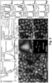
- the size and size distribution of InSb CQDs could be well-controlled by precisely adjusting the precursor conversion kinetics. This adjustment allows for the separation of the nucleation and growth processes and avoids the secondary nucleation. To do so, it was adopted the "single-source" precursor approach via a continuous precursor injection process instead of hot-injection, which allowed to obtain InSb CQDs with well-controlled size distribution and distinct excitonic peaks over a very broad range (900 nm to 1750 nm). As shown in Fig.
- the absorption spectra of InSb CQDs exhibit clear excitonic peaks, without any size selective precipitation, whose positions were controlled by reaction temperatures from 220 °C to 250 °C (see Experimental Methods below).
- the powder X-ray diffraction patterns (XRD) shown in Fig. 1b revealed a pure cubic zinc blende crystal structure of InSb CQDs, identical to that of bulk InSb. The width of diffraction peaks clearly narrows with increasing size, which is consistent with the Scherrer equation.
- TEM images confirmed the InSb CQDs with average size of 2.4 nm, 3.0 nm, 3.5 nm, 4.4 nm, 5.8 nm and 7.0 nm that is corresponding to the first exciton peak at 905 nm, 1020 nm, 1120 nm, 1260 nm, 1520 nm and 1750 nm respectively.
- the present inventors also found that the relationship between size and bandgap of InSb CQDs in their case is very close to the sizing curve reported by Busatto et al. [7].
- the present inventors have then further characterized the surface of the manufactured InSb CQDs, for it is known to play a key role in the optoelectronic properties of CQD materials. It has been proved the trap states of III-V CQDs originate from unpassivated dangling bonds of the surface [8]. Specifically, the dangling bonds of group V elements create much deeper trap states than group III, resulting detrimental consequences on their optoelectronic properties. X-ray photoelectron spectroscopy (XPS) analysis was performed to probe the oxidation states of Sb that corresponding to unpassivated Sb dangling bond of the surface. Fig 2g exhibits the Sb 3d XPS spectra, showing strong evidence of Sb-oxide formation (detail discussions see below). Hence, it is urgent to develop passivation strategy for the obtained InSb CQDs.
- XPS X-ray photoelectron spectroscopy
- cadmium is a heavy metal element, and on the other hand, it was noticed that InSb surface can react with Te, forming In 2 Te 3 and Sb at elevated temperatures [15].
- this treatment partially passivated the surface dangling bonds of Sb to reduce defects, and on the other hand, it improved the colloidal stability of InSb CQDs in subsequent purification processes.
- the InSb CQDs treated with InCl 3 exhibited a very clear first exciton absorption peak at 1020 nm.
- indium oleate and phosphine silylamide (P[N(Si(Me) 3 ) 2 ] 3 ) were used as precursors to grow 0.5 layer (i.e., to partially cover the InSb core) and 1 layer (i.e., to fully cover the InSb core) of InP shell on the purified InSb CQDs respectively.
- the absorption spectrum of InSb CQDs exhibit a significant red shift of approximately 120 nm to 1140 nm rather than a blue shift after the InP shell growth ( Fig. 2a ). This indicates a successful core-shell structure instead of alloying.
- III-V covalent semiconductors are expected to show much better thermal stability that is a prerequisite for wafer level integration and overall device stability.
- PbS CQD films lose their quantum confinement above 150 °C [16] due to CQD fusion and necking.
- the obtained InSb CQD films show good stability at 150 °C with some redshift.
- the III-Vs InSb is the compound with lowest melting point, the present inventors posited therefore that the use of a shell made of InP (that has much higher melting point) would lend thermal stability to the final CQD.
- the InSb/lnP core-shell CQD films exhibit improved thermal stability preserving their quantum confinement even at 200 °C, as shown in Fig.
- Photoluminescence (PL) spectra were first used to confirm the InSb/InP core-shell structure, as shown in Fig. 2b , the PL intensity of InSb CQDs increased by 3000 times after the InP shell growth.
- the present inventors then further calculated the absolute PL quantum yield (PLQY) by the integration sphere method [17], and it showed that the InSb/lnP core-shell CQDs achieved a PLQY of 3.7% at 1300 nm ( Fig. 6 ), which is the first report for InSb CQDs to date.
- Fig. 2c shows the XRD patterns of corresponding InSb core and InSb/lnP core-shell structure.
- the diffraction peak of InSb core at 23.8° shifts to higher angle at 24.3° after the InP shell growth.
- the InSb core still maintains the crystal structure of zinc blende, and no extra diffraction peaks belonging to InP were observed. This suggests that pure InSb/lnP core-shell structure was obtained without any phase segregation.
- TEM images confirmed the shape of CQDs evolved from near-spherical ( Fig. 7 left) to tetrahedrally faceted after the growth of InP shell ( Fig. 7 right), which is in agreement with Liu et al.
- HAADF-STEM High angle annular dark field scanning transmission electron microscopy (HAADF-STEM, Fig. 2d ) image showed the same lattice constant as InSb, indicating that no alloying structure has formed.
- FFT fast Fourier transform
- EDX energy-dispersive X-ray spectroscopy
- XPS measurement was further employed to study the surface of InSb CQDs after InP shell growth.
- the proportion of Sb-O bonds at 539.9 eV and 530.6 eV in the pristine InSb CQDs is up to 34%, which indicates the presence of a large number of unpassivated Sb dangling bonds on the surface, probably acting as the trap states.
- it was decreased to 28% after the in-situ surface post-treatment with InCI3.
- this value was further decreased to 7.5% or even disappeared completely after the growth of InP shell.
- the present inventors aimed to implement them into a low-temperature, solution-processed, SWIR photodetector.
- InI 3 was chosen to replace the surface organic long chain ligand of InSb CQDs [2], performing a solid-state ligand exchange method.
- FTIR Fourier transform infrared
- the conduction band, valence band, and Fermi level of the InSb and InSb/InP core shell CQDs film were measured by the ultraviolet photoelectron spectroscopy (UPS, Fig. 10 ).
- UPS ultraviolet photoelectron spectroscopy
- the present inventors first designed a vertical device architecture consisting of indium-tin oxide (ITO)/ZnO/InSb/MoO x /Au.
- ITO indium-tin oxide
- ZnO Zinctron spectroscopy
- the present inventors then sought to perform annealing of the ZnO layer, which led to drastic deterioration of the rectification followed however by a dramatic increase of the measured EQE under bias.
- EQE was measured to exceed 100% under bias suggests that the device in those conditions exhibits some photoconductive gain. This was further supported by the EQE dependence on the modulation frequency up to 222 Hz ( Fig. 12 ) and the slow response time of the detector under bias ( Fig. 13 ).
- This photoconductor gain effect has also been observed in PbS QD devices by using ZnO as the electron transfer layer (ETL) and is ascribed to photogenerated carrier trapping in the ZnO layer due to photochemical reactions [19].
- the present inventors were, instead, interested to address applications that go beyond video frame rate imaging such as gated imaging or indirect time-of-flight (iToF) which require detectors with faster response times ( ⁇ 100 ns).
- the present inventors thus turned to the use of TiO 2 as the ETL which is known to exhibit photochemical stability as opposed to ZnO.
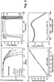
- the device architecture and band alignment are shown in Figs. 3a and 3b , where, for the illustrated embodiment, the device comprises:.
- the current density-voltage (J-V) characteristic of pristine InSb CQDs photodetector exhibits poor rectification and low performance with EQE of 3% at 1100 nm under zero bias ( Fig. 14 ).
- the rectification and external quantum efficiency (EQE) of InSb/lnP core-shell CQDs photodetector have shown significant improvement ( Figs. 3c-f ), which suggests that our surface passivation strategy is effective.
- the EQE of InSb/InP CQDs photodetector with 0.5L InP shell is 5% at 1250 nm under 0V bias, and it reaches 25% under 2V bias.
- the EQE of InSb/InP CQDs photodetector with 1L InP shell is 1.8% at 1300 nm under 0V bias, and it reaches 15% under 1.5V bias ( Fig. 3f ).
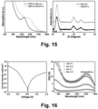
- the present inventors also performed core-shell growth on larger-sized InSb CQDs. As shown in Fig. 15 , the exciton absorption peak of the InSb/lnP CQDs moved from 1180 nm to 1380 nm. Based on these InSb/InP core-shell CQDs, the corresponding photodetector was fabricated and the highest EQE of 12% at 1420 nm under bias was achieved ( Fig. 16 ).
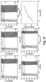
- the present inventors assessed air stability of InSb/InP CQDs photodetector ( Fig. 17 ). Remarkably, even after two months of exposure to the ambient environment without any encapsulation, the device maintains its rectification properties and nearly identical EQE levels, demonstrating resilience to atmospheric conditions. Moreover, the present inventors investigated the thermal stability of the InSb/lnP CQD photodetectors ( Fig. 18 ). The obtained findings suggest that the device remains stable when subjected to annealing temperatures below 150 °C, pointing to a much better thermal stability than Pb-chalcogenide CQD counterparts.
- the frequency response measurement of InSb/InP CQDs photodetector was carried out to calculate the 3dB bandwidth.
- the 3dB bandwidth could be limited by the resistor-capacitor (RC) time constant or carrier mobility depending on the thickness of active layer.
- the present inventors measured the bias-dependent 3dB bandwidth ( Fig. 19 ), the absence of bandwidth dependence on bias supports an RC-limited instead of mobility-limited 3dB bandwidth. Since the RC time is directly related to the device area, the device area-dependent 3dB bandwidth was measured. As shown in Fig. 4a and Fig.
- the 3dB bandwidth increased from 850 kHz to 6 MHz when the device area decreased from 3.1mm 2 to 0.09 mm 2 .
- the transient response with different device areas revealed the falling-time reduction from 1.65 ⁇ s to 70 ns, respectively, in accordance with the observed 3dB bandwidth.
- the linear dynamic range (LDR) of InSb/InP CQDs photodetector was measured by varying the incident light intensity. As shown in Fig. 4c , the photocurrent maintained linearity with incident light power over a broad range and LDR is estimated to be over 128 dB.
- the frequency-dependent current noise spectrum of InSb/InP CQDs photodetector was measured with fast Fourier Transform (FFT) current transients for low frequency and a lock-in amplifier for high frequency range ( Fig. 22 ).
- the obtained noise spectrum showed a 1/f noise dominating at low frequency and a generation-recombination noise at high frequency.
- the device reaches a noise floor of ⁇ 3 * 10 -15 A Hz -0.5 at frequency of 300 kHz.
- the InSb/lnP CQDs photodetector reached a maximum of D* ⁇ 3.6 ⁇ 10 12 Jones at 300 kHz at 1240 nm ( Fig. 4d ), and the frequency dependent D*was provided in Fig. 23 .
- Oleylamine Oleylamine (OLA, 80-90%) and Tris(trimethylsily)phosphine ((TMS) 3 P, 98%) were purchased from Thermal Scientific.
- Tris(dimethylamido)antimony-(III) Sb[NMe 2 ] 3 , 99.99%) and indium(III) chloride (InCl 3 , 99.999%) were purchased from Strem Chemicals.
- Indium acetate In(OAc) 3 , 99.99%
- indium(III) iodide InI 3 , 99.998%
- 1-octadecene ODE, 90%
- lithium triethylborohydride LiEt 3 BH, SuperHydride, 1 M in tetrahydrofuran, THF
- dioctyl ether DOE, 99%
- oleic acid OA, 90%
- methanol anhydrous, 99.8%
- toluene anhydrous, 99.8%
- Acetone anhydrous, 98%) was purchased from Scharlab. All chemicals were used as received except for oleylamine and oleic acid, which were degassed before use. The degassing was performed at 100 °C under reduced pressure ( ⁇ 1 mbar) for 4 h.
- LiEt 3 BH (1.0 M) dissolved in tetrahydrofuran (THF) is used as purchased. A 100 mL amount of the superhydride solution is added to 50 mL of degassed dioctyl ether (DOE) and then evacuated on the Schlenk line for >4 h, until the THF is completely removed. Caution: LiEt 3 BH is very reactive in air and should be handled using air-free processes. The final superhydride solution has a concentration of 2.0 M in DOE.
- DOE degassed dioctyl ether
- TMS 3 P solution 1 mL (TMS) 3 P solution was mixed with 16 mL degassed ODE, and the 0.2 M (TMS) 3 P-ODE solution was formed.
- reaction solution was transferred into the plastic centrifuge tubes inside the glovebox.
- the reaction mixture was separated in two portions, oleic acid (2 mL) was added to each and rotated for 2 min. Then 24 mL of MeOH was added, leading to turbidity. Centrifugation for 10 min at 6000 rpm yielded a black precipitate and colorless supernatant. The colorless supernatant was discarded, and the black precipitate was redispersed in 10 mL of toluene, and centrifugation for more 10 min at 6000 rpm. The precipitate was discarded, then 2 mL oleic acid was added to the supernatant, and 15 mL of MeOH was added.
- UV-vis absorption measurements were performed with a Cary 5000 UV-Vis-NIR spectroscope in solution.
- PL photoluminescence
- four channel Thorlabs laser was used as excitation light and a Kymera 328i spectrograph (Oxford Instruments, Andor) was used as the detector ( ⁇ 1600 nm).
- a 935 nm laser, an integration sphere and the Andor detector were used.
- the XRD data were collected using a Rigaku SmartLab powder diffractometer in the Bragg-Brentano geometry with Cu K ⁇ radiation on drop-casted powder samples.
- TEM was performed at the Scientific and Technological Centres of the University of Barcelona.
- the TEM images were obtained using a JEOL 2100F microscope operating at an accelerating voltage of 200 kV.
- TEM samples were prepared by dropping diluted QD solution on ultrathin carbon grids.
- Scanning transmission electron microscopy (STEM) experiments were conducted using an FEI Titan G2 80-200 microscope at 200 kV equipped with a Cs-probe corrector and a HAADF detector. Elemental maps were taken by energy-dispersive X-ray spectroscopy (EDX) using four large-solid-angle symmetrical Si drift detectors.
- EDX energy-dispersive X-ray spectroscopy
- the XPS/UPS measurements were performed with a SPECS PHOIBOS 150 hemispherical analyser under ultrahigh-vacuum conditions (10 -10 mbar) at the Institut Català de Nanociència i Nanotecnologia.
- ITO-covered glass substrates (Universtician Stuttgart, Institut für Proflambaige Mikroelektronik) were cleaned by sonication in soapy water, acetone and isopropanol for 20 min each and dried with nitrogen, followed with 30 min ultraviolet/ozone treatment. TiOz electron transport layer was then deposited with a sputtering technique to achieve a thickness of ⁇ 40 nm. Three layers of InSb/InP CQDs were further spin-coated from 50 mg ml -1 toluene solution via the layer-by-layer method.
- InSb/lnP CQDs layer For each InSb/lnP CQDs layer, one drop of InSb/InP CQDs solution was spin coated onto TiO 2 /ITO substrates during spinning (2,000 r.p.m.). Then, 5 mg ml -1 InI 3 /Methanol solution was applied to the CQDs film for 30 s, followed by two rinse-spin steps with methanol and once with toluene. Finally, a Kurt J. Lesker NANO 36 system was used to deposit 10 nm MoO x as the electronic blocking layer and 100 nm Au as top electrode with a device area of 3.1 mm 2 . The device with smaller device area was deposited with the special shadow mask.
- the output current was recorded with an oscilloscope.
- four-channel laser (Thorlabs) at 1310 nm was used as light source at a frequency of 7 Hz modulated by Agilent waveform generator. The light was directed by a beam-splitter to a Newport 818-IG detector and the device. The current was amplified by an SR570 amplifier and recorded by an oscilloscope.
- devices were connected with Stanford Research SR830 lock-in amplifier directly.
Landscapes
- Chemical & Material Sciences (AREA)
- Engineering & Computer Science (AREA)
- Materials Engineering (AREA)
- Organic Chemistry (AREA)
- Inorganic Chemistry (AREA)
- Light Receiving Elements (AREA)
Priority Applications (2)
| Application Number | Priority Date | Filing Date | Title |
|---|---|---|---|
| EP23383278.1A EP4570878A1 (fr) | 2023-12-12 | 2023-12-12 | Population de points quantiques comprenant des points quantiques insb, procédé d'obtention de la population de points quantiques et dispositif optoélectronique comprenant la population de points quantiques |
| PCT/EP2024/085957 WO2025125454A1 (fr) | 2023-12-12 | 2024-12-12 | Population de points quantiques comprenant des points quantiques insb, procédé d'obtention de la population de points quantiques et dispositif optoélectronique comprenant la population de points quantiques |
Applications Claiming Priority (1)
| Application Number | Priority Date | Filing Date | Title |
|---|---|---|---|
| EP23383278.1A EP4570878A1 (fr) | 2023-12-12 | 2023-12-12 | Population de points quantiques comprenant des points quantiques insb, procédé d'obtention de la population de points quantiques et dispositif optoélectronique comprenant la population de points quantiques |
Publications (1)
| Publication Number | Publication Date |
|---|---|
| EP4570878A1 true EP4570878A1 (fr) | 2025-06-18 |
Family
ID=89222331
Family Applications (1)
| Application Number | Title | Priority Date | Filing Date |
|---|---|---|---|
| EP23383278.1A Pending EP4570878A1 (fr) | 2023-12-12 | 2023-12-12 | Population de points quantiques comprenant des points quantiques insb, procédé d'obtention de la population de points quantiques et dispositif optoélectronique comprenant la population de points quantiques |
Country Status (2)
| Country | Link |
|---|---|
| EP (1) | EP4570878A1 (fr) |
| WO (1) | WO2025125454A1 (fr) |
-
2023
- 2023-12-12 EP EP23383278.1A patent/EP4570878A1/fr active Pending
-
2024
- 2024-12-12 WO PCT/EP2024/085957 patent/WO2025125454A1/fr active Pending
Non-Patent Citations (20)
| Title |
|---|
| ASOR, L ET AL.: "Zn-doped P-type InAs nanocrystal quantum dots", ADV. MATER., vol. 35, 2023, pages 2208332 |
| BUSATTO, S ET AL.: "Luminescent colloidal InSb quantum dots from in situ generated single-source precursor", ACS NANO, vol. 14, 2020, pages 13146 - 13160, XP093089566, DOI: 10.1021/acsnano.0c04744 |
| D. V. KRYLSKY: "Synthesis, Composition, Photoluminescence, and Stability of Properties of Colloidal InSb-Based Quantum Dots", TECHNICAL PHYSICS LETTERS., vol. 45, no. 8, 1 August 2019 (2019-08-01), US, pages 801 - 804, XP093163860, ISSN: 1063-7850, Retrieved from the Internet <URL:http://link.springer.com/article/10.1134/S106378501908025X/fulltext.html> [retrieved on 20240517], DOI: 10.1134/S106378501908025X * |
| FU, HZUNGER, A: "InP quantum dots: electronic structure, surface effects, and the redshifted emission", PHYS. REV. B, vol. 56, 1997, pages 1496 |
| GOLDBERY, Y. A.LEVINSHTEIN, M.RUMYANTSEV, S.SHUR, M., E.: "Handbook series on semiconductor parameters", vol. 1, 1996, WORLD SCIENTIFIC, pages: 191 - 213 |
| HUGHES, K. E.STEIN, J. L.FRIEDFELD, M. R.COSSAIRT, B. M.GAMELIN D. R.: "Effects of surface chemistry on the photophysics of colloidal InP nanocrystals", ACS NANO, vol. 13, 2019, pages 14198 - 14207 |
| JEAN, J ET AL.: "Radiative efficiency limit with band tailing exceeds 30% for quantum dot solar cells", ACS ENERGY LETT, vol. 2, 2017, pages 2612 - 2624 |
| KIM, T ET AL.: "Trap passivation in indium-based quantum dots through surface fluorination: mechanism and applications", ACS NANO, vol. 12, 2018, pages 11529 - 11540 |
| LEEMANS, J ET AL.: "Colloidal III-V quantum dot photodiodes for short-wave infrared photodetection", ADV. SCI., vol. 9, 2022, pages 2200844 |
| LIU, W.CHANG, A. Y.SCHALLER, R. D.TALAPIN, D. V.: "Colloidal InSb nanocrystals", J. AM. CHEM. SOC., vol. 134, 2012, pages 20258 - 20261, XP055283656, DOI: 10.1021/ja309821j |
| MELLO, J. C.WITTMANN, H. F.FRIEND, R. H.: "An improved experimental determination of external photoluminescence quantum efficiency", ADV. MATER., vol. 9, 1997, pages 230 - 232, XP000682004, DOI: 10.1002/adma.19970090308 |
| NAJARIAN, A. M. ET AL.: "Sub-millimetre light detection and ranging using perovskites", NAT. ELECTRON., vol. 5, 2022, pages 511 - 518 |
| SAGAR, L. K. ET AL.: "Single-precursor intermediate shelling enables bright, narrow line width InAs/InZnP-based QD emitters", CHEM. MATER., vol. 32, 2020, pages 2919 - 2925 |
| SUBHASHRI CHATTERJEE: "Solution-Processed InSb Quantum Dot Photodiodes for Short-Wave Infrared Sensing", ACS APPLIED NANO MATERIALS, vol. 6, no. 17, 17 August 2023 (2023-08-17), pages 15540 - 15550, XP093163859, ISSN: 2574-0970, Retrieved from the Internet <URL:https://pubs.acs.org/doi/pdf/10.1021/acsanm.3c02221> [retrieved on 20240517], DOI: 10.1021/acsanm.3c02221 * |
| SUN, B ET AL.: "Fast near-infrared photodetection using III-V colloidal quantum dots", ADV. MATER., vol. 34, 2022, pages 2203039 |
| XIE, RPENG, X: "Synthetic scheme for high-quality InAs nanocrystals based on self-focusing and one-pot synthesis of InAs-based core-shell nanocrystals", ANGEW. CHEM. INT. ED., vol. 47, 2008, pages 7677 - 7680, XP055771590, DOI: 10.1002/anie.200802867 |
| XU, K ET AL.: "Large photomultiplication by charge-self-trapping for high-response quantum dot infrared photodetectors", ACS APPL. MATER. INTERFACES, vol. 14, 2022, pages 14783 - 14790 |
| ZAHN, D. R. T. ET AL.: "Raman spectroscopy of InSb/CdTe heterostructures: improved interface quality obtained by Cd overpressure during molecular beam epitaxial growth", APPL. PHYS. LETT., vol. 53, 1988, pages 2409 - 2410, XP000026003, DOI: 10.1063/1.100245 |
| ZHAO, T ET AL.: "General synthetic route to high-quality colloidal III-V semiconductor quantum dots based on pnictogen chlorides", J. AM. CHEM. SOC., vol. 141, 2019, pages 15145 - 15152, XP093113424, DOI: 10.1021/jacs.9b06652 |
| ZHAO, X.LIM, L. J.ANG, S. S.TAN, Z.: "Efficient short-wave infrared light-emitting diodes based on heavy-metal-free quantum dots", ADV. MATER., vol. 34, 2022, pages 2206409 |
Also Published As
| Publication number | Publication date |
|---|---|
| WO2025125454A1 (fr) | 2025-06-19 |
Similar Documents
| Publication | Publication Date | Title |
|---|---|---|
| Hafiz et al. | Colloidal quantum dots for thermal infrared sensing and imaging | |
| Peng et al. | InSb/InP core–shell colloidal quantum dots for sensitive and fast short-wave infrared photodetectors | |
| US10749058B2 (en) | Monodisperse, IR-absorbing nanoparticles and related methods and devices | |
| Ren et al. | Evidences of sensitization mechanism for PbSe thin films photoconductor | |
| Li et al. | Ga₂O₃/V₂O₅ oxide heterojunction photovoltaic photodetector with superhigh solar-blind spectral discriminability | |
| Muhammad et al. | Fabrication of ultra-violet photodetector with enhanced optoelectronic parameters using low-cost F-doped ZnO nanostructures | |
| Patra et al. | Investigations on LSPR effect of Cu/Al nanostructures on ZnO nanorods towards photodetector applications | |
| US20190172960A1 (en) | Solar cells and methods of making solar cells | |
| US12426406B2 (en) | Dislocation free semiconductor nanostructures grown by pulse laser deposition with no seeding or catalyst | |
| Hu et al. | Colloidal InAs quantum dots: synthesis, properties, and optoelectronic devices | |
| Manimozhi et al. | Enhanced photo-response of CdTe Thin film via Mo doping prepared using electron beam evaporation technique | |
| Lee et al. | Giant colloidal quantum dot/α-Ga2O3 heterojunction for high performance UV–Vis–IR broadband photodetector | |
| Saha et al. | Investigation of Yttrium (Y)-doped ZnO (Y: ZnO)–Ga2O3 core-shell nanowire/Si vertical heterojunctions for high-performance self-biased wideband photodetectors | |
| Cui et al. | Mid-infrared plasmonic silicon quantum dot/HgCdTe photodetector with ultrahigh specific detectivity | |
| Chalapathi et al. | Synthesis of AgBiS2 films by sulfurizing Bi/Ag stacks for thin film photovoltaics | |
| Ponomarenko et al. | Photoelectronics based on 0D materials | |
| Zhang et al. | Heavy metal-free colloidal quantum dots: preparation and application in infrared photodetectors | |
| Maurya et al. | Advancements in AgBiS2 thin film solar cells: strategies, challenges, and perspectives | |
| Bhatt et al. | Wafer-scale, thickness-controlled p-CuInSe2/n-Si heterojunction for self-biased, highly sensitive, and broadband photodetectors | |
| Kim et al. | Monolithic green-sensitive photodetectors enabled by a ZnSnN 2/GaN nanorods/silicon double heterojunction | |
| WO2025125454A1 (fr) | Population de points quantiques comprenant des points quantiques insb, procédé d'obtention de la population de points quantiques et dispositif optoélectronique comprenant la population de points quantiques | |
| Liu et al. | MgZnO-based Schottky barrier ultraviolet-b photodiode by ultrasonic spray pyrolysis deposition | |
| Ma et al. | Colloidal InSb Quantum Dots for Short-Wave Infrared Photodetection | |
| KR102949009B1 (ko) | 광전 소자 및 이의 제조방법 | |
| Nawwar et al. | Thermal evaporation fabrication of UV-NIR p–i–n photodetectors based on highly tensile-strained Ge via incorporation of Pb rather than Sn and As |
Legal Events
| Date | Code | Title | Description |
|---|---|---|---|
| PUAI | Public reference made under article 153(3) epc to a published international application that has entered the european phase |
Free format text: ORIGINAL CODE: 0009012 |
|
| STAA | Information on the status of an ep patent application or granted ep patent |
Free format text: STATUS: THE APPLICATION HAS BEEN PUBLISHED |
|
| AK | Designated contracting states |
Kind code of ref document: A1 Designated state(s): AL AT BE BG CH CY CZ DE DK EE ES FI FR GB GR HR HU IE IS IT LI LT LU LV MC ME MK MT NL NO PL PT RO RS SE SI SK SM TR |
|
| STAA | Information on the status of an ep patent application or granted ep patent |
Free format text: STATUS: REQUEST FOR EXAMINATION WAS MADE |
|
| 17P | Request for examination filed |
Effective date: 20251203 |